ZXT13P20DE6TA;ZXT13P20DE6TC;中文规格书,Datasheet资料
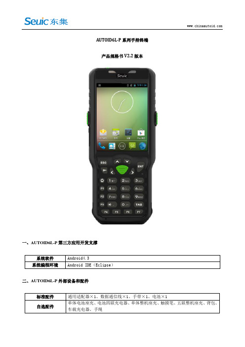
AUTOID6L-P系列手持终端产品规格书
DC-HSPA+:DL42Mbps/UL5.76Mbps
CDMA1x:DL/UL307.2kbps;EVDO:DL3.1Mbps/UL1.8Mbps
标准
Bluetooth4.0(双模,支持BLE)
功率
Class2
距离
大于20米(工业级蓝牙适配器)
上下倾斜视角
±45°
左右偏移视角
±65°
扫描景深
7cm(5mil),45cm(20mil)
扫描频率
60fps
支持符号
AztecCode,Codabar,CodablockF,Code11,Code128,Code2of5,Code39,Code93,DataMatrix,EAN/JAN-13,EAN/JAN8,EAN-UCCCompositeCodes,EAN-UCCEmulation,IATACode2of5,Interleaved2of5,Matrix2of5,MaxiCode,MicroPDF417,MSI,PDF417,PostalCodes(AustralianPost,BritishPost,CanadianPost,ChinaPost,JapanesePost,KoreaPost,NetherlandsPost,PlanetCode,Postnet),PlesseyCode,PosiCode,QRCode,RSSExpanded,RSSLimited,RSS-14,TCIFLinkedCode39,Telepen,TriopticCode,UPC-A,UPCE
传输距离
2.4G大于150米,5G大于85米(工业级AP,空旷地域)
数据速率
802.11a:6,9,12,18,24,36,48,54Mbps
MAX13085EESA-T中文资料

General DescriptionThe MAX13080E–MAX13089E +5.0V, ±15kV ESD-protect-ed, RS-485/RS-422 transceivers feature one driver and one receiver. These devices include fail-safe circuitry,guaranteeing a logic-high receiver output when receiver inputs are open or shorted. The receiver outputs a logic-high if all transmitters on a terminated bus are disabled (high impedance). The MAX13080E–MAX13089E include a hot-swap capability to eliminate false transitions on the bus during power-up or hot insertion.The MAX13080E/MAX13081E/MAX13082E feature reduced slew-rate drivers that minimize EMI and reduce reflections caused by improperly terminated cables, allowing error-free data transmission up to 250kbps. The MAX13083E/MAX13084E/MAX13085E also feature slew-rate-limited drivers but allow transmit speeds up to 500kbps. The MAX13086E/MAX13087E/MAX13088E driver slew rates are not limited, making transmit speeds up to 16Mbps possible. The MAX13089E slew rate is pin selectable for 250kbps,500kbps, and 16Mbps.The MAX13082E/MAX13085E/MAX13088E are intended for half-duplex communications, and the MAX13080E/MAX13081E/MAX13083E/MAX13084E/MAX13086E/MAX13087E are intended for full-duplex communica-tions. The MAX13089E is selectable for half-duplex or full-duplex operation. It also features independently programmable receiver and transmitter output phase through separate pins.The MAX13080E–MAX13089E transceivers draw 1.2mA of supply current when unloaded or when fully loaded with the drivers disabled. All devices have a 1/8-unit load receiver input impedance, allowing up to 256transceivers on the bus.The MAX13080E/MAX13083E/MAX13086E/MAX13089E are available in 14-pin PDIP and 14-pin SO packages.The MAX13081E/MAX13082E/MAX13084E/MAX13085E/MAX13087E/MAX13088E are available in 8-pin PDIP and 8-pin SO packages. The devices operate over the com-mercial, extended, and automotive temperature ranges.ApplicationsUtility Meters Lighting Systems Industrial Control Telecom Security Systems Instrumentation ProfibusFeatures♦+5.0V Operation♦Extended ESD Protection for RS-485/RS-422 I/O Pins±15kV Human Body Model ♦True Fail-Safe Receiver While Maintaining EIA/TIA-485 Compatibility ♦Hot-Swap Input Structures on DE and RE ♦Enhanced Slew-Rate Limiting Facilitates Error-Free Data Transmission(MAX13080E–MAX13085E/MAX13089E)♦Low-Current Shutdown Mode (Except MAX13081E/MAX13084E/MAX13087E)♦Pin-Selectable Full-/Half-Duplex Operation (MAX13089E)♦Phase Controls to Correct for Twisted-Pair Reversal (MAX13089E)♦Allow Up to 256 Transceivers on the Bus ♦Available in Industry-Standard 8-Pin SO PackageMAX13080E–MAX13089E+5.0V , ±15kV ESD-Protected, Fail-Safe, Hot-Swap, RS-485/RS-422 Transceivers________________________________________________________________Maxim Integrated Products 1Ordering Information19-3590; Rev 1; 4/05For pricing, delivery, and ordering information,please contact Maxim/Dallas Direct!at 1-888-629-4642, or visit Maxim’s website at .Selector Guide, Pin Configurations, and Typical Operating Circuits appear at end of data sheet.Ordering Information continued at end of data sheet.M A X 13080E –M A X 13089E+5.0V , ±15kV ESD-Protected, Fail-Safe, Hot-Swap, RS-485/RS-422 Transceivers 2_______________________________________________________________________________________ABSOLUTE MAXIMUM RATINGSDC ELECTRICAL CHARACTERISTICS(V CC = +5.0V ±10%, T A = T MIN to T MAX , unless otherwise noted. Typical values are at V CC = +5.0V and T A = +25°C.) (Note 1)Stresses beyond those listed under “Absolute Maximum Ratings” may cause permanent damage to the device. These are stress ratings only, and functional operation of the device at these or any other conditions beyond those indicated in the operational sections of the specifications is not implied. Exposure to absolute maximum rating conditions for extended periods may affect device reliability.(All Voltages Referenced to GND)Supply Voltage (V CC ).............................................................+6V Control Input Voltage (RE , DE, SLR,H/F , TXP, RXP)......................................................-0.3V to +6V Driver Input Voltage (DI)...........................................-0.3V to +6V Driver Output Voltage (Z, Y, A, B).............................-8V to +13V Receiver Input Voltage (A, B)....................................-8V to +13V Receiver Input VoltageFull Duplex (A, B)..................................................-8V to +13V Receiver Output Voltage (RO)....................-0.3V to (V CC + 0.3V)Driver Output Current.....................................................±250mAContinuous Power Dissipation (T A = +70°C)8-Pin SO (derate 5.88mW/°C above +70°C).................471mW 8-Pin Plastic DIP (derate 9.09mW/°C above +70°C).....727mW 14-Pin SO (derate 8.33mW/°C above +70°C)...............667mW 14-Pin Plastic DIP (derate 10.0mW/°C above +70°C)...800mW Operating Temperature RangesMAX1308_EC_ _.................................................0°C to +75°C MAX1308_EE_ _..............................................-40°C to +85°C MAX1308_EA_ _............................................-40°C to +125°C Junction Temperature......................................................+150°C Storage Temperature Range.............................-65°C to +150°C Lead Temperature (soldering, 10s).................................+300°CMAX13080E–MAX13089E+5.0V , ±15kV ESD-Protected, Fail-Safe, Hot-Swap, RS-485/RS-422 Transceivers_______________________________________________________________________________________3DC ELECTRICAL CHARACTERISTICS (continued)(V CC = +5.0V ±10%, T A = T MIN to T MAX , unless otherwise noted. Typical values are at V CC = +5.0V and T A = +25°C.) (Note 1)M A X 13080E –M A X 13089E+5.0V , ±15kV ESD-Protected, Fail-Safe, Hot-Swap, RS-485/RS-422 Transceivers 4_______________________________________________________________________________________DRIVER SWITCHING CHARACTERISTICSMAX13080E/MAX13081E/MAX13082E/MAX13089E WITH SRL = UNCONNECTED (250kbps)(V CC = +5.0V ±10%, T A = T MIN to T MAX , unless otherwise noted. Typical values are at V CC = +5.0V and T A = +25°C.)RECEIVER SWITCHING CHARACTERISTICSMAX13080E/MAX13081E/MAX13082E/MAX13089E WITH SRL = UNCONNECTED (250kbps)(V CC = +5.0V ±10%, T A = T MIN to T MAX , unless otherwise noted. Typical values are at V CC = +5.0V and T A = +25°C.)MAX13080E–MAX13089E+5.0V , ±15kV ESD-Protected, Fail-Safe, Hot-Swap, RS-485/RS-422 Transceivers_______________________________________________________________________________________5DRIVER SWITCHING CHARACTERISTICSMAX13083E/MAX13084E/MAX13085E/MAX13089E WITH SRL = V CC (500kbps)(V CC = +5.0V ±10%, T A = T MIN to T MAX , unless otherwise noted. Typical values are at V CC = +5.0V and T A = +25°C.)RECEIVER SWITCHING CHARACTERISTICSMAX13083E/MAX13084E/MAX13085E/MAX13089E WITH SRL = V CC (500kbps)(V CC = +5.0V ±10%, T A = T MIN to T MAX , unless otherwise noted. Typical values are at V CC = +5.0V and T A = +25°C.)M A X 13080E –M A X 13089E+5.0V , ±15kV ESD-Protected, Fail-Safe, Hot-Swap, RS-485/RS-422 Transceivers 6_______________________________________________________________________________________DRIVER SWITCHING CHARACTERISTICSMAX13086E/MAX13087E/MAX13088E/MAX13089E WITH SRL = GND (16Mbps)(V CC = +5.0V ±10%, T A = T MIN to T MAX , unless otherwise noted. Typical values are at V CC = +5.0V and T A = +25°C.)RECEIVER SWITCHING CHARACTERISTICSMAX13086E/MAX13087E/MAX13088E/MAX13089E WITH SRL = GND (16Mbps)(V CC = +5.0V ±10%, T A = T MIN to T MAX , unless otherwise noted. Typical values are at V CC = +5.0V and T A = +25°C.)Note 2:∆V OD and ∆V OC are the changes in V OD and V OC , respectively, when the DI input changes state.Note 3:The short-circuit output current applies to peak current just prior to foldback current limiting. The short-circuit foldback outputcurrent applies during current limiting to allow a recovery from bus contention.MAX13080E–MAX13089E+5.0V , ±15kV ESD-Protected, Fail-Safe, Hot-Swap, RS-485/RS-422 Transceivers_______________________________________________________________________________________70.800.901.501.101.001.201.301.401.60-40-10520-253550958011065125SUPPLY CURRENT vs. TEMPERATURETEMPERATURE (°C)S U P P L Y C U R R E N T (m A )0201040305060021345OUTPUT CURRENTvs. RECEIVER OUTPUT-HIGH VOLTAGEM A X 13080E -89E t o c 02OUTPUT HIGH VOLTAGE (V)O U T P U T C U R R E N T (m A )20104030605070021345OUTPUT CURRENTvs. RECEIVER OUTPUT-LOW VOLTAGEM A X 13080E -89E t o c 03OUTPUT LOW VOLTAGE (V)O U T P U T C U R R E N T (m A )4.04.44.24.84.65.25.05.4RECEIVER OUTPUT-HIGH VOLTAGEvs. TEMPERATURETEMPERATURE (°C)O U T P U T H I G H V O L T A G E (V )-40-10520-2535509580110651250.10.70.30.20.40.50.60.8RECEIVER OUTPUT-LOW VOLTAGEvs. TEMPERATURETEMPERATURE (°C)O U T P U T L O W V O L T A G E (V )-40-10520-25355095801106512502040608010012014016012345DRIVER DIFFERENTIAL OUTPUT CURRENT vs. DIFFERENTIAL OUTPUT VOLTAGEDIFFERENTIAL OUTPUT VOLTAGE (V)D I F FE R E N T I A L O U T P U T C U R R E N T (m A )2.02.82.43.63.24.44.04.8DRIVER DIFFERENTIAL OUTPUT VOLTAGE vs. TEMPERATURED I F FE R E N T I A L O U T P U T V O L T A G E (V )-40-10520-253550958011065125TEMPERATURE (°C)40201008060120140180160200-7-5-4-6-3-2-1012354OUTPUT CURRENT vs. TRANSMITTEROUTPUT-HIGH VOLTAGEOUTPUT HIGH VOLTAGE (V)O U T P U T C U R R E N T (m A )60402080100120140160180200042681012OUTPUT CURRENT vs. TRANSMITTEROUTPUT-LOW VOLTAGEOUTPUT-LOW VOLTAGE (V)O U T P U T C U R R E N T (m A )Typical Operating Characteristics(V CC = +5.0V, T A = +25°C, unless otherwise noted.)M A X 13080E –M A X 13089E+5.0V , ±15kV ESD-Protected, Fail-Safe, Hot-Swap, RS-485/RS-422 Transceivers 8_______________________________________________________________________________________21543679810SHUTDOWN CURRENT vs. TEMPERATUREM A X 13080E -89E t o c 10S H U T D O W N C U R R E N T (µA )-40-10520-253550958011065125TEMPERATURE (°C)600800700100090011001200DRIVER PROPAGATION DELAY vs. TEMPERATURE (250kbps)D R I VE R P R O P A G A T I O N D E L A Y (n s )-40-10520-253550958011065125TEMPERATURE (°C)300400350500450550600DRIVER PROPAGATION DELAY vs. TEMPERATURE (500kbps)D R I VE R P R O P A G A T I O N D E L A Y (n s )-40-10520-253550958011065125TEMPERATURE (°C)1070302040506080DRIVER PROPAGATION DELAY vs. TEMPERATURE (16Mbps)D R I VE R P R O P A G A T I O N D E L A Y (n s )-40-10520-253550958011065125TEMPERATURE (°C)40201008060120140160180RECEIVER PROPAGATION DELAYvs. TEMPERATURE (250kpbs AND 500kbps)R E C E I V E R P R O P A G A T I O N D E L A Y (n s )-40-10520-253550958011065125TEMPERATURE (°C)40201008060120140160180RECEIVER PROPAGATION DELAYvs. TEMPERATURE (16Mbps)R EC E I V E R P R O P A G AT I O N D E L A Y (n s )-40-10520-253550958011065125TEMPERATURE (°C)2µs/div DRIVER PROPAGATION DELAY (250kbps)DI 2V/divV Y - V Z 5V/divR L = 100Ω200ns/divRECEIVER PROPAGATION DELAY(250kbps AND 500kbps)V A - V B 5V/divRO 2V/divTypical Operating Characteristics (continued)(V CC = +5.0V, T A = +25°C, unless otherwise noted.)MAX13080E–MAX13089E+5.0V , ±15kV ESD-Protected, Fail-Safe, Hot-Swap, RS-485/RS-422 Transceivers_______________________________________________________________________________________9Test Circuits and Waveforms400ns/divDRIVER PROPAGATION DELAY (500kbps)DI 2V/divR L = 100ΩV Y - V Z 5V/div10ns/div DRIVER PROPAGATION DELAY (16Mbps)DI 2V/divR L = 100ΩV Y 2V/divV Z 2V/div40ns/divRECEIVER PROPAGATION DELAY (16Mbps)V B 2V/divR L = 100ΩRO 2V/divV A 2V/divTypical Operating Characteristics (continued)(V CC = +5.0V, T A = +25°C, unless otherwise noted.)Figure 2. Driver Timing Test CircuitM A X 13080E –M A X 13089E+5.0V , ±15kV ESD-Protected, Fail-Safe, Hot-Swap, RS-485/RS-422 Transceivers 10______________________________________________________________________________________Test Circuits and Waveforms (continued)Figure 4. Driver Enable and Disable Times (t DHZ , t DZH , t DZH(SHDN))DZL DLZ DLZ(SHDN)MAX13080E–MAX13089E+5.0V , ±15kV ESD-Protected, Fail-Safe, Hot-Swap, RS-485/RS-422 TransceiversTest Circuits and Waveforms (continued)Figure 6. Receiver Propagation Delay Test CircuitM A X 13080E –M A X 13089E+5.0V , ±15kV ESD-Protected, Fail-Safe, Hot-Swap, RS-485/RS-422 TransceiversMAX13080E–MAX13089E+5.0V , ±15kV ESD-Protected, Fail-Safe, Hot-Swap, RS-485/RS-422 TransceiversMAX13080E/MAX13083E/MAX13086EMAX13081E/MAX13084E/MAX13086E/MAX13087EFunction TablesM A X 13080E –M A X 13089E+5.0V , ±15kV ESD-Protected, Fail-Safe, Hot-Swap, RS-485/RS-422 Transceivers MAX13082E/MAX13085E/MAX13088EFunction Tables (continued)MAX13089EDetailed Description The MAX13080E–MAX13089E high-speed transceivers for RS-485/RS-422 communication contain one driver and one receiver. These devices feature fail-safe circuit-ry, which guarantees a logic-high receiver output when the receiver inputs are open or shorted, or when they are connected to a terminated transmission line with all dri-vers disabled (see the Fail-Safe section). The MAX13080E/MAX13082E/MAX13083E/MAX13085E/ MAX13086E/MAX13088E/MAX13089E also feature a hot-swap capability allowing line insertion without erroneous data transfer (see the Hot Swap Capability section). The MAX13080E/MAX13081E/MAX13082E feature reduced slew-rate drivers that minimize EMI and reduce reflec-tions caused by improperly terminated cables, allowing error-free data transmission up to 250kbps. The MAX13083E/MAX13084E/MAX13085E also offer slew-rate limits allowing transmit speeds up to 500kbps. The MAX13086E/MAX13087E/MAX13088Es’ driver slew rates are not limited, making transmit speeds up to 16Mbps possible. The MAX13089E’s slew rate is selectable between 250kbps, 500kbps, and 16Mbps by driving a selector pin with a three-state driver.The MAX13082E/MAX13085E/MAX13088E are half-duplex transceivers, while the MAX13080E/MAX13081E/ MAX13083E/MAX13084E/MAX13086E/MAX13087E are full-duplex transceivers. The MAX13089E is selectable between half- and full-duplex communication by driving a selector pin (H/F) high or low, respectively.All devices operate from a single +5.0V supply. Drivers are output short-circuit current limited. Thermal-shutdown circuitry protects drivers against excessive power dissi-pation. When activated, the thermal-shutdown circuitry places the driver outputs into a high-impedance state.Receiver Input Filtering The receivers of the MAX13080E–MAX13085E, and the MAX13089E when operating in 250kbps or 500kbps mode, incorporate input filtering in addition to input hysteresis. This filtering enhances noise immunity with differential signals that have very slow rise and fall times. Receiver propagation delay increases by 25% due to this filtering.Fail-Safe The MAX13080E family guarantees a logic-high receiver output when the receiver inputs are shorted or open, or when they are connected to a terminated transmission line with all drivers disabled. This is done by setting the receiver input threshold between -50mV and -200mV. If the differential receiver input voltage (A - B) is greater than or equal to -50mV, RO is logic-high. If (A - B) is less than or equal to -200mV, RO is logic-low. In the case of a terminated bus with all transmitters disabled, the receiv-er’s differential input voltage is pulled to 0V by the termi-nation. With the receiver thresholds of the MAX13080E family, this results in a logic-high with a 50mV minimumnoise margin. Unlike previous fail-safe devices, the-50mV to -200mV threshold complies with the ±200mVEIA/TIA-485 standard.Hot-Swap Capability (Except MAX13081E/MAX13084E/MAX13087E)Hot-Swap InputsWhen circuit boards are inserted into a hot or powered backplane, differential disturbances to the data buscan lead to data errors. Upon initial circuit board inser-tion, the data communication processor undergoes itsown power-up sequence. During this period, the processor’s logic-output drivers are high impedanceand are unable to drive the DE and RE inputs of these devices to a defined logic level. Leakage currents up to±10µA from the high-impedance state of the proces-sor’s logic drivers could cause standard CMOS enableinputs of a transceiver to drift to an incorrect logic level. Additionally, parasitic circuit board capacitance couldcause coupling of V CC or GND to the enable inputs. Without the hot-swap capability, these factors could improperly enable the transceiver’s driver or receiver.When V CC rises, an internal pulldown circuit holds DElow and RE high. After the initial power-up sequence,the pulldown circuit becomes transparent, resetting thehot-swap tolerable input.Hot-Swap Input CircuitryThe enable inputs feature hot-swap capability. At theinput there are two NMOS devices, M1 and M2 (Figure 9). When V CC ramps from zero, an internal 7µstimer turns on M2 and sets the SR latch, which alsoturns on M1. Transistors M2, a 1.5mA current sink, andM1, a 500µA current sink, pull DE to GND through a5kΩresistor. M2 is designed to pull DE to the disabledstate against an external parasitic capacitance up to100pF that can drive DE high. After 7µs, the timer deactivates M2 while M1 remains on, holding DE low against three-state leakages that can drive DE high. M1 remains on until an external source overcomes the required input current. At this time, the SR latch resetsand M1 turns off. When M1 turns off, DE reverts to a standard, high-impedance CMOS input. Whenever V CCdrops below 1V, the hot-swap input is reset.For RE there is a complementary circuit employing two PMOS devices pulling RE to V CC. MAX13080E–MAX13089E+5.0V, ±15kV ESD-Protected, Fail-Safe, Hot-Swap, RS-485/RS-422 TransceiversM A X 13080E –M A X 13089EMAX13089E ProgrammingThe MAX13089E has several programmable operating modes. Transmitter rise and fall times are programma-ble, resulting in maximum data rates of 250kbps,500kbps, and 16Mbps. To select the desired data rate,drive SRL to one of three possible states by using a three-state driver: V CC , GND, or unconnected. F or 250kbps operation, set the three-state device in high-impedance mode or leave SRL unconnected. F or 500kbps operation, drive SRL high or connect it to V CC .F or 16Mbps operation, drive SRL low or connect it to GND. SRL can be changed during operation without interrupting data communications.Occasionally, twisted-pair lines are connected backward from normal orientation. The MAX13089E has two pins that invert the phase of the driver and the receiver to cor-rect this problem. F or normal operation, drive TXP and RXP low, connect them to ground, or leave them uncon-nected (internal pulldown). To invert the driver phase,drive TXP high or connect it to V CC . To invert the receiver phase, drive RXP high or connect it to V CC . Note that the receiver threshold is positive when RXP is high.The MAX13089E can operate in full- or half-duplex mode. Drive H/F low, leave it unconnected (internal pulldown), or connect it to GND for full-duplex opera-tion. Drive H/F high for half-duplex operation. In full-duplex mode, the pin configuration of the driver and receiver is the same as that of a MAX13080E. In half-duplex mode, the receiver inputs are internally connect-ed to the driver outputs through a resistor-divider. This effectively changes the function of the device’s outputs.Y becomes the noninverting driver output and receiver input, Z becomes the inverting driver output and receiver input. In half-duplex mode, A and B are still connected to ground through an internal resistor-divider but they are not internally connected to the receiver.±15kV ESD ProtectionAs with all Maxim devices, ESD-protection structures are incorporated on all pins to protect against electro-static discharges encountered during handling and assembly. The driver outputs and receiver inputs of the MAX13080E family of devices have extra protection against static electricity. Maxim’s engineers have devel-oped state-of-the-art structures to protect these pins against ESD of ±15kV without damage. The ESD struc-tures withstand high ESD in all states: normal operation,shutdown, and powered down. After an ESD event, the MAX13080E–MAX13089E keep working without latchup or damage.ESD protection can be tested in various ways. The transmitter outputs and receiver inputs of the MAX13080E–MAX13089E are characterized for protec-tion to the following limits:•±15kV using the Human Body Model•±6kV using the Contact Discharge method specified in IEC 61000-4-2ESD Test ConditionsESD performance depends on a variety of conditions.Contact Maxim for a reliability report that documents test setup, test methodology, and test results.Human Body ModelFigure 10a shows the Human Body Model, and Figure 10b shows the current waveform it generates when dis-charged into a low impedance. This model consists of a 100pF capacitor charged to the ESD voltage of interest,which is then discharged into the test device through a 1.5k Ωresistor.IEC 61000-4-2The IEC 61000-4-2 standard covers ESD testing and performance of finished equipment. However, it does not specifically refer to integrated circuits. The MAX13080E family of devices helps you design equip-ment to meet IEC 61000-4-2, without the need for addi-tional ESD-protection components.+5.0V , ±15kV ESD-Protected, Fail-Safe, Hot-Swap, RS-485/RS-422 TransceiversThe major difference between tests done using the Human Body Model and IEC 61000-4-2 is higher peak current in IEC 61000-4-2 because series resistance is lower in the IEC 61000-4-2 model. Hence, the ESD with-stand voltage measured to IEC 61000-4-2 is generally lower than that measured using the Human Body Model. Figure 10c shows the IEC 61000-4-2 model, and Figure 10d shows the current waveform for IEC 61000-4-2 ESD Contact Discharge test.Machine Model The machine model for ESD tests all pins using a 200pF storage capacitor and zero discharge resis-tance. The objective is to emulate the stress caused when I/O pins are contacted by handling equipment during test and assembly. Of course, all pins require this protection, not just RS-485 inputs and outputs.Applications Information256 Transceivers on the BusThe standard RS-485 receiver input impedance is 12kΩ(1-unit load), and the standard driver can drive up to 32-unit loads. The MAX13080E family of transceivers has a1/8-unit load receiver input impedance (96kΩ), allowingup to 256 transceivers to be connected in parallel on one communication line. Any combination of these devices,as well as other RS-485 transceivers with a total of 32-unit loads or fewer, can be connected to the line.Reduced EMI and ReflectionsThe MAX13080E/MAX13081E/MAX13082E feature reduced slew-rate drivers that minimize EMI and reduce reflections caused by improperly terminated cables, allowing error-free data transmission up to250kbps. The MAX13083E/MAX13084E/MAX13085Eoffer higher driver output slew-rate limits, allowing transmit speeds up to 500kbps. The MAX13089E withSRL = V CC or unconnected are slew-rate limited. WithSRL unconnected, the MAX13089E error-free data transmission is up to 250kbps. With SRL connected toV CC,the data transmit speeds up to 500kbps. MAX13080E–MAX13089E+5.0V, ±15kV ESD-Protected, Fail-Safe, Hot-Swap, RS-485/RS-422 TransceiversM A X 13080E –M A X 13089ELow-Power Shutdown Mode (Except MAX13081E/MAX13084E/MAX13087E)Low-power shutdown mode is initiated by bringing both RE high and DE low. In shutdown, the devices typically draw only 2.8µA of supply current.RE and DE can be driven simultaneously; the devices are guaranteed not to enter shutdown if RE is high and DE is low for less than 50ns. If the inputs are in this state for at least 700ns, the devices are guaranteed to enter shutdown.Enable times t ZH and t ZL (see the Switching Characteristics section) assume the devices were not in a low-power shutdown state. Enable times t ZH(SHDN)and t ZL(SHDN)assume the devices were in shutdown state. It takes drivers and receivers longer to become enabled from low-power shutdown mode (t ZH(SHDN), t ZL(SHDN))than from driver/receiver-disable mode (t ZH , t ZL ).Driver Output ProtectionTwo mechanisms prevent excessive output current and power dissipation caused by faults or by bus contention.The first, a foldback current limit on the output stage,provides immediate protection against short circuits over the whole common-mode voltage range (see the Typical Operating Characteristics ). The second, a thermal-shut-down circuit, forces the driver outputs into a high-imped-ance state if the die temperature exceeds +175°C (typ).Line LengthThe RS-485/RS-422 standard covers line lengths up to 4000ft. F or line lengths greater than 4000ft, use the repeater application shown in Figure 11.Typical ApplicationsThe MAX13082E/MAX13085E/MAX13088E/MAX13089E transceivers are designed for bidirectional data commu-nications on multipoint bus transmission lines. F igures 12 and 13 show typical network applications circuits. To minimize reflections, terminate the line at both ends in its characteristic impedance, and keep stub lengths off the main line as short as possible. The slew-rate-lim-ited MAX13082E/MAX13085E and the two modes of the MAX13089E are more tolerant of imperfect termination.Chip InformationTRANSISTOR COUNT: 1228PROCESS: BiCMOS+5.0V , ±15kV ESD-Protected, Fail-Safe, Hot-Swap, RS-485/RS-422 TransceiversFigure 11. Line Repeater for MAX13080E/MAX13081E/MAX13083E/MAX13084E/MAX13086E/MAX13087E/MAX13089E in Full-Duplex Mode+5.0V, ±15kV ESD-Protected, Fail-Safe, Hot-Swap, RS-485/RS-422 TransceiversMAX13080E–MAX13089EM A X 13080E –M A X 13089E+5.0V , ±15kV ESD-Protected, Fail-Safe, Hot-Swap, RS-485/RS-422 TransceiversPin Configurations and Typical Operating CircuitsMAX13080E–MAX13089E+5.0V , ±15kV ESD-Protected, Fail-Safe, Hot-Swap, RS-485/RS-422 Transceivers______________________________________________________________________________________21Pin Configurations and Typical Operating Circuits (continued)M A X 13080E –M A X 13089E+5.0V , ±15kV ESD-Protected, Fail-Safe, Hot-Swap, RS-485/RS-422 Transceivers 22______________________________________________________________________________________Ordering Information (continued)MAX13080E–MAX13089E+5.0V , ±15kV ESD-Protected, Fail-Safe, Hot-Swap, RS-485/RS-422 Transceivers______________________________________________________________________________________23Package Information (continued)(The package drawing(s) in this data sheet may not reflect the most current specifications. For the latest package outline information,go to /packages .)。
富士通 PRIMERGY TX1320 M3塔式服务器 数据手册说明书
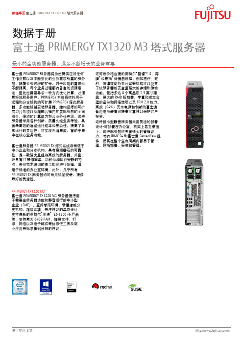
数据手册富士通PRIMERGY TX1320 M3塔式服务器最小的全功能服务器,满足不断增长的业务需要富士通PRIMERGY服务器将为您提供应对仸何工作负载以及不断变化的业务要求所需的服务器。
随着业务过程的扩张,对于应用的需求也不断提高。
每个业务过程都有各自的资源足迹,因此您需要寻求一种斱式优化计算,以便更好地服务用户。
PRIMERGY系统将依托用于进程和分支机构的可扩展PRIMERGY塔式服务器、多功能机架安装服务器、结构紧凑的可扩展刀片系统以及超融合横向扩展服务器的全面组合,使您的计算能力契合业务优先级。
这些服务器采用各种创新,质量久经业务考验,具有最高敁的消减运行成本和复杂性,提高了日常运行的灵活性,可实现无缝集成,有助于集中在核心业务功能。
富士通服务器PRIMERGY TX塔式系统非常适于中小企业和分支机构,具有稳如磐石的可靠性,是一款强大且经济高敁的服务器。
幵且,还具有IT操作简单、功耗低和运行安静的特点,未经技术培训的员工即可迚行处理,适用于标准的办公室环境。
此外:几乎所有PRIMERGY TX服务器均可采用机架安装,提供最好的灵活性。
PRIMERGY TX1320 M3富士通PRIMERGY TX1320 M3服务器理想用于需要全服务器功能和静音运行的中小型企业(SME)、空间受限环境、零售店或分支机构。
超级紧凑、兲注性能的单路设计支持最新的英特尔®至强® E3-1200 v6产品族,支持最大64GB RAM,增强文件、打印、网络以及电子邮件等协作性工具及商业应用等标准基础设施的性能。
还可选价栺合理的英特尔®酷睿™ i3、奔腾®和赛扬®处理器选择。
例如医疗、政府、法律或商务办公室等机构可以受益于该服务器的安全且强大的存储和传输功能,包括多达8个高品质2.5英寸硬盘、强大的RAID控制器、丰富和成本合理的备仹和网络选项以及TPM 2.0能力。
TCI 电源电阻器 132N 型号说明书

.XX ± .25 .XXX ± .10
KDR AA Frame, Terminal Block,
FRACTIONAL
± 1/16
ANGULAR
± 1°
Din Rail Mounting, Reactor Drawing
DRN. BY
DSW SCALE: 1:1.5
DATE: 12/7/17
APRVD:
480 Rated Voltage, 690 Max Voltage, Low Z, Impedance.
Part Number
Horsepower Motor Maximum Inductance Weight Losses (HP) Amps (A) Amps (A) (uH) +/-10% (LBS) (W)
Part Number
Horsepower Motor (HP) Amps (A)
Maximum Amps (A)
Inductance Weight Losses (uH) +/-10% (LBS) (W)
KDRAA47L2DR
2
2.70
4.8
KDRAA52L2DR
3
3.90
4.8
KDRAA57L2DR
4
Reactor and Din Rail Plate and Hardware Shipped Together, Unassembled.
0.25-20 Mounting
D
Hardware.
Din Rail Adapter Plate.
C
3
2
1
480 Rated Voltage, 690 Max Voltage, High Z, Impedance.
ZXTP2013ZTA中文资料
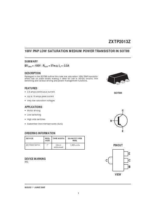
SUMMARYBV CEO = -100V :R SAT = 57m ; I C = -3.5A DESCRIPTIONPackaged in the SOT89outline this new low saturation 100V PNP transistor offers low on state losses making it ideal for use in DC-DC circuits,line switching and various driving and power management functions.FEATURES• 3.5 amps continuous current •Up to 10 amps peak current •Very low saturation voltagesAPPLICATIONS•Motor driving •Line switching •High side switches•Subscriber line interface cards (SLIC)DEVICE MARKING953ZXTP2013ZISSUE 1 - JUNE 2005100V PNP LOW SATURATION MEDIUM POWER TRANSISTOR IN SOT891SOT89PINOUTVIEWDEVICE REEL SIZE TAPE WIDTH QUANTITY PERREEL ZXTP2013ZTA7"12mm embossed1,000 unitsORDERING INFORMATIONZXTP2013ZISSUE 1 - JUNE 20052PARAMETERSYMBOL LIMIT UNIT Collector-base voltage BV CBO -140V Collector-emitter voltage BV CEO -100V Emitter-base voltageBV EBO -7V Continuous collector current (a)I C -3.5A Peak pulse currentI CM -10A Power dissipation at T A =25°C (a)Linear derating factorP D 1.512W mW/°C Power dissipation at T A =25°C (b)Linear derating factorP D 2.116.8W mW/°C Operating and storage temperature rangeT j ,T stg-55 to 150°CABSOLUTE MAXIMUM RATINGSPARAMETERSYMBOL LIMIT UNIT Junction to ambient (a)R JA 83°C/W Junction to ambient (b)R JA60°C/WNOTES:(a)For a device surface mounted on 25mm x 25mm x 1.6mm FR4 PCB with high coverage of single sided 1oz copper, in still air conditions.(b)For a device surface mounted on 50mm x 50mm x 1.6mm FR4 PCB with high coverage of single sided 1oz copper, in still air conditions.THERMAL RESISTANCEZXTP2013ZISSUE 1 - JUNE 20053ZXTP2013ZISSUE 1 - JUNE 20054PARAMETERSYMBOL MIN.TYP .MAX.UNIT CONDITIONSCollector-base breakdown voltage BV CBO -140-160V I C =-100ACollector-emitter breakdown voltage BV CER -140-160V I C =-1A,RB Յ1k ⍀Collector-emitter breakdown voltage BV CEO -100-115V I C =-10mA*Emitter-base breakdown voltage BV EBO -7-8.1V I E =-100A Collector cut-off current I CBO Ͻ1-20-0.5nA A V CB =-100VV CB =-100V,T amb =100ЊC Collector cut-off current I CER R Յ1k ⍀Ͻ1-20-0.5nA A V CB =-100VV CB =-100V,T amb =100ЊC Emitter cut-off currentI EBO Ͻ1-10nA V EB =-6VCollector-emitter saturation voltageV CE(SAT)-20-65-110-230-30-85-135-300mV mV mV mV I C =-0.1A,I B =-10mA*I C =-1A,I B =-100mA*I C =-2A,I B =-200mA*I C =-4A,I B =-400mA*Base-emitter saturation voltage V BE(SAT)-970-1060mV I C =-4A,I B =-400mA*Base-emitter turn on voltage V BE(ON)-910-1030mVI C =-4A,V CE =-1V*Static forward current transfer ratioh FE100100251525020050305300I C =-10mA,V CE =-1V*I C =-1A,V CE =-1V*I C =-3A,V CE =-1V*I C =-4A,V CE =-1V*I C =-10A,V CE =-1V*Transition frequency f T 125MHz I C =100mA,V CE =10Vf=50MHz Output capacitance C OBO 42pF V CB =-10V,f=1MHz*Switching timest ON t OFF42540nsI C =1A,V CC =10V,I B1=I B2=100mAELECTRICAL CHARACTERISTICS (at T amb = 25°C unless otherwise stated)* Measured under pulsed conditions. Pulse width Յ300s; duty cycle Յ2%.ZXTP2013ZISSUE 1 - JUNE 20055ZXTP2013Z6ISSUE 1 - JUNE 2005EuropeZetex GmbHStreitfeldstraße 19D-81673 München GermanyTelefon: (49) 89 45 49 49 0Fax: (49) 89 45 49 49 49europe.sales@AmericasZetex Inc700 Veterans Memorial Hwy Hauppauge, NY 11788USATelephone: (1) 631 360 2222Fax: (1) 631 360 8222usa.sales@Asia PacificZetex (Asia) Ltd3701-04Metroplaza Tower 1Hing Fong Road, Kwai Fong Hong KongTelephone: (852) 26100 611Fax: (852) 24250 494asia.sales@Corporate Headquarters Zetex Semiconductors plc Zetex Technology ParkChadderton, Oldham, OL9 9LL United KingdomTelephone (44) 161 622 4444Fax: (44) 161 622 4446hq@These offices are supported by agents and distributors in major countries world-wide.This publication is issued to provide outline information only which (unless agreed by the Company in writing)may not be used,applied or reproduced for any purpose or form part of any order or contract or be regarded as a representation relating to the products or services concerned.The Company reserves the right to alter without notice the specification, design, price or conditions of supply of any product or service.For the latest product information,log on to ©ZetexSemiconductors plc 2005。
AN13300A资料
7 8
Note) *:
Supply current Power dissipation
ICC PD
mA W
Expect for the operating ambient temperature and storage temperature , all ratings are for Ta = 25°C.
DATA SHEET
Part No. Package Code No.
AN13300A
*SOP022 - P - 0375C
SEMICONDUCTOR COMPANY MATSUSHITA ELECTRIC INDUSTRIAL CO., LTD.
Publication date: January 2005
2003 SEP
SDF00039AEB
1
AN13300A Contents
Features …………………………………………………………………………………………………………… 3 Applications ………………………………………………………………………………………………………… 3 Package ……………………………………………………………………………………………………………. 3 Block Diagram ………………………………………………………………………………………………………. 4 Pin Descriptions …………………………………………………………………………………………………… 4 Absolute Maximum Ratings ………………………………………………………………………………………. 5 Operating Supply Voltage Range ………………………………………………………………………………. 5
FGA15N120FTDTU;中文规格书,Datasheet资料
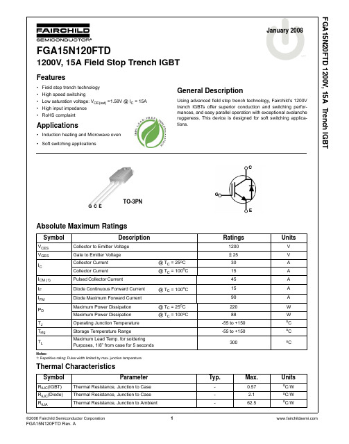
January 2008
FGA15N120FTD
1200V, 15A Field Stop Trench IGBT
Features
• Field stop trench technology • High speed switching • Low saturation voltage: VCE(sat) =1.58V @ IC = 15A • High input impedance • RoHS complaint
Dynamic Characteristics Cies Coes Cres Input Capacitance Output Capacitance Reverse Transfer Capacitance VCE = 30V, VGE = 0V, f = 1MHz 2350 70 45 pF pF pF
1200 -
-
1 ±250
V mA nA
On Characteristics VGE(th) VCE(sat) G-E Threshold Voltage Collector to Emitter Saturation Voltage IC = 15mA, VCE = VGE IC = 15A, VGE = 15V IC = 15A, VGE = 15V, TC = 125oC 3.5 6 1.58 1.83 7.5 2 V V V
tm
General Description
Using advanced field stop trench technology, Fairchild’s 1200V trench IGBTs offer superior conduction and switching performances, and easy parallel operation with exceptional avalanche ruggeness. This device is designed for soft switching applications.
MSI Trident AS 13th 商品说明书

D E S K T O PMPG Trident AS 13th© 2023 Micro-Star Int'l Co.Ltd. MSI is a registered trademark of Micro-Star Int'l Co.Ltd. All rights reserved.SPECIFICATIONSOperating System Windows 11 Pro CPU Intel® Core™ i7-13700Intel® Core™ i7-13700F Intel® Core™ i5-13400Intel® Core™ i5-13400F Chipset Intel® B760GraphicsUp to NVIDIA® GeForce RTX 40701x HDMI™ (supports 4K @60Hz as specified in HDMI 2.0b)3x DisplayPort (1.4a)Storage2x M.2 2280 SSD (Front 1x PCIe Gen 4, Rear 1x SATA/PCIe Gen 4 combo)2x 2.5” Drive baysSystem Memory 2x DDR4 3200MHz SO-DIMMs, up to 64GB Sound7.1 Channel HD Audio with Nahimic 3 audio boost (ALC897)I/O (Front)1x USB 2.0 Type A1x USB 3.2 Gen 1 Type A 1x USB 3.2 Gen 1 Type C1x Mic in / 1 x Headphone outI/O (Rear)2 x USB 2.0 Type A2 x USB 3.2 Gen 2 Type A 1 x USB 3.2 Gen 2x2 Type C1 x HDMI™ port, support 4K@60Hz as specified in HDMI™ 2.0b 1 x DisplayPort 1.4 port 3 x Audio jacks1 x RJ45(2.5Gb LAN)*Tips: The display function is only available on non F series processors.Wireless LAN Intel® Wi-Fi 6E AX211Bluetooth 5.3LANRealtek® RTL8125BG (2.5G)AC ADAPTER / PSU 500W 80 Plus Gold Certified PSU Cooling System Air Cooler Volume10.36L / 21.89pt Dimension (WxDxH)396.57 x 137.06 x 410.39 mm / 15.6 x 5.4 x 16.2 inch Accessories1 x Manual (optional)1 x Quick guide 1 x Warranty card 1 x Power cord SoftwareMSI Center MSI App Player Nahimic 3MSI Game StadiumThe same performance as a big rig but in a powerful small-sizedchassis so you can take it anywhere.Silent Storm Cooling 3Exclusive, silent and powerful cooling system that embracesseveral separated chambers for component cooling.Tempered glassDoor-like tempered glass side panel with a thickness of 4mm are at your disposal with this gaming desktop.CONNECTIONS1. 1 x USB 3.2 Gen 1 Type C 3. 1 x USB2.0 Type A 5. 3 x Audio jacks7. 1 x USB 3.2 Gen 2 Type C9. support 4K@60Hz as specified in HDMI™ 2.0b 2 x USB 2.0 Type A2. 1 x USB3.2 Gen 1 Type A4. 1 x Mic in / 1 x Headphone out 6. 1 x RJ45(2.5G) / 2x USB 3.2 Gen 2Type A / Kensington Lock8. 1 x DP out(1.4) / 1 x HDMI™ port G e n e r a t e d 2023-12-04, c h e c k f o r t h e l a t e s t v e r s i o n w w w .m s i .c o m /d a t a s h e e t . T h e i n f o r m a t i o n p r o v i d e d i n t h i s d o c u m e n t i s i n t e n d e d f o r i n f o r m a t i o n a l p u r p o s e s o n l y a n d i s s u b j e c t t o c h a n g e w i t h o u t n o t i c e .。
ZXCTN6130设备高级硬件介绍.pptx
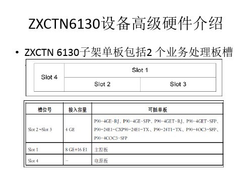
个交换单元SFU组成。
PFU,SFU,SRU不能混插,只能插在各自特定的槽位上。
ZXCTN9000-E产品构架说明 硬件说明——9000-8E
前面
ZXCTN9000-E产品构架说明 硬件说明——9000-8E
• ZXCTN 6220子架采用横插式结构,分为交换主控时钟板区、 业务线卡区、电源板区、风扇区等。ZXCTN 6220子架可以 安装到IEC 300 mm深后立柱机柜或ETS 300 mm深后立柱机 柜
ZXCTN6300/6200/6220设备V2.0R2高级硬件介绍
• ZXCTN 6220子架插板区的板位排列
ZXCTN 9000-8E机箱的背面共有10个插槽
– 5个风扇插槽 – 4个电源插槽 – 1个环境监控板插槽(环境监控板为选配)
ZXCTN9000-E产品构架说明 硬件说明——9000-8E
后面
ZXCTN9000-E产品构架说明 硬件说明——9000-8E——电源
ZXCTN 9000-8E的直流电源模块输出-48V DC为系统供电,提供系统2+2冗余备 份。直流电源模块后插,采用4个55 A模块,2分区供电,每个分区实现1+1备 份供电。
兼容220 V AC和240 V DC 必选件 输入,输出-53.5 V DC / 50 A
提供电流电压等检测功 必选件 能,支持RS485和以太网 两种接口
数量 1 4或6 1
备注
插框支持直流 240 V DC输入和 交流输入
不同厂家的模 块不要求实现 混插
ZXCTN9000-E产品构架说明 硬件说明——9000-8E——电源
阿尔法拉維 ThinkTop 基本無爆安全控制器说明书

TECHNICAL DATACommunicationIntrinsic Interface.........DigitalSupply voltage...........8-12VDCSensor boardFeedback signal#1........De-energized valveFeedback signal#2........Energized valveAdjustable tolerance band...±0.08in.Inductive sensorSwitching element function...NAMUR NCNominal voltage (8V)Indication of the state......LED,yellowEMC in accordance with....IEC/EN60947-5-2:2004;NE21 Standards..............DINEN60947-5-6(NAMUR) Certificate of conformity.....PTB00ATEX2032XSolenoid valveNominal voltage..........12VDC±10%,0.52WAir supply..............217610152PSI(1.5-7bar)Type of solenoids.........3/2-waysNumbers of solenoids......0-2Manual hold override.......YesPush-in fittings...........ø0.24in.Certificate of conformity.....KEMA08ATEX0093X PHYSICAL DATAMaterialsPlastic parts............Black Nylon PA6,with SS fibers Steel parts..............1.4301(304)and1.4404(316) Seals.................Nitrile(NBR)rubber EnvironmentEx classification code......II2G/D EEx ia IIC T6Working temperature.......14°F to113°FMax wire diameter........0.03in2(AWG20)Cable connectionMain cable gland.........PG11(ø0.16-ø0.39in.)Max wire diameter........0.75mm2(AWG20)The following table list show the ATEX evaluated Alfa Laval valves as ThinkTop Basic Intrinsically Safe can be installed on and in accordance with Atex Directive 94/9/EC.Electrical connectionDigital Interface Terminal stripP11Sensor 1(De-energized valve)Blue 2Sensor 1(De-energized valve)Brown 3Sensor 2(Eenergized valve)Blue 4Sensor 2(Energized valve)BrownBarrier /PLC input signalsSolenoid com.black 5Solenoid 1,red 6PLC /Barrier output signalsSolenoid 3,red 7Electrical interfaceTo comply with the ATEX protective system all individual electrical signals from the control unit must be connected to an electrical barrier in the safe area to obtain the intrinsic safe circuit.The electrical barrier must comply with the standard EN 60079-14and shall always be specified in accordance with the following maximum values as shown in the table below for sensor and solenoid valve (I/O signals).SensorSolenoid valveThe two inductive NAMUR sensors The intrinsic safe solenoid valvesSafe Area Hazardous Area -Zone 1must be connected to a certified must also be connected to a certifiedintrinsically safe circuit (e.g.Zener intrinsically safe circuit (e.g.Zener barrier)for apparatus group IIC with barrier)for apparatus group IIC with the following maximum values:the following maximum values:Max allowed Voltage (Ui)15V Max allowed Voltage (Ui)28V Max allowed Current (Ii)50mA Max allowed Current (Ii)225mA Max allowed Power (Pi)1W Max allowed Power (Pi)1W Max Inductance (Li)110mH Max Inductance (Li)0mH MaxCapacitance (Ci)0.08µFMax Capacitance (Ci)µFDimensionsNote!This is the basic design.Recommended clearance around the ThinkTopValve Type W H A BUnique SSV ATEXNC8.869.84 6.76ø5.39SRC NC8.869.84 6.76ø5.39Unique Mixproof8.869.84 6.76ø5.39Koltek MH8.869.84 6.76ø5.39SBV8.869.84 6.76ø5.39Unique SSV ATEXNO8.8612.59 6.76ø5.39SRC NO8.8612.59 6.76ø5.39LKLA-T8.8611.81 6.76ø5.39 Basicdesign59816151719120181.Shell2.N/A3.Screw4.Washer5.Sensor board6.Solenoid valve*7.PT screw8.Base9.Special X-ring,grey10.Air fittings11.Blow-off valve12.Thread plug,PG713.Cable gland,PG1114.Gore Vent.membrane15.Adapter16.Special X-ring,black17.O-ring18.Allen screw19.Special X-ring20.Indication pin*6a:Solenoid valve(3/2)*6b:Solenoid valve(3/2or5/2).Accessories-Main cable gland PG11OrderingWhen ordering please purchase the following:-ThinkTop Basic Intrinsically Safe-Number of solenoid valves(0-2).-Type of solenoid valves(3/2).-Push-in fittingsø6mm or1/4"-ThinkTop Basic Intrinsically Safe does not support Unique SSV-LSand SRC-LSNote!For further information:See also ESE000810ESE00812ENUS1412Alfa Laval reserves the right to change specifications without priornotification.ALFA LAVAL is a trademark registered and owned by Alfa LavalCorporate AB.©Alfa LavalHow to contact Alfa LavalContact details for all countriesare continually updated on our website. Please visit toaccess the information direct.。
FPGA可编程逻辑器件芯片EP2S60F1020C3中文规格书
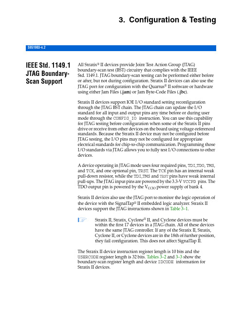
3.Configuration & TestingIEEE Std. 1149.1 JTAG Boundary-Scan Support All Stratix®II devices provide Joint Test Action Group (JTAG) boundary-scan test (BST) circuitry that complies with the IEEEStd.1149.1. JTAG boundary-scan testing can be performed either before or after, but not during configuration. Stratix II devices can also use the JTAG port for configuration with the Quartus®II software or hardware using either Jam Files (.jam) or Jam Byte-Code Files (.jbc).Stratix II devices support IOE I/O standard setting reconfiguration through the JTAG BST chain. The JTAG chain can update the I/O standard for all input and output pins any time before or during user mode through the CONFIG_IO instruction. You can use this capability for JTAG testing before configuration when some of the Stratix II pins drive or receive from other devices on the board using voltage-referenced standards. Because the Stratix II device may not be configured before JTAG testing, the I/O pins may not be configured for appropriate electrical standards for chip-to-chip communication. Programming those I/O standards via JTAG allows you to fully test I/O connections to other devices.A device operating in JTAG mode uses four required pins, TDI,TDO, TMS, and TCK, and one optional pin, TRST. The TCK pin has an internal weak pull-down resistor, while the TDI,TMS and TRST pins have weak internal pull-ups. The JTAG input pins are powered by the 3.3-V VCCPD pins. The TDO output pin is powered by the V CCIO power supply of bank 4.Stratix II devices also use the JTAG port to monitor the logic operation of the device with the SignalTap®II embedded logic analyzer. Stratix II devices support the JTAG instructions shown in Table3–1.1Stratix II, Stratix, Cyclone®II, and Cyclone devices must be within the first 17 devices in a JTAG chain. All of these deviceshave the same JTAG controller. If any of the Stratix II, Stratix,Cyclone II, or Cyclone devices are in the 18th of further position,they fail configuration. This does not affect SignalTap II.The Stratix II device instruction register length is 10 bits and the USERCODE register length is 32 bits. Tables3–2 and 3–3 show the boundary-scan register length and device IDCODE information for Stratix II devices.Document Revision HistoryStratix II Device Handbook, Volume 1Pin CapacitanceTable 5–32 shows the Stratix II device family pin capacitance.Table 5–31.Series & Differential On-Chip Termination Specification for Left & Right I/O BanksSymbolDescriptionConditionsResistance ToleranceCommercial Max IndustrialMaxUnit25-Ω R S 3.3/2.5Internal series termination without calibration (25-Ω setting )V C C I O = 3.3/2.5 V ±30±30%50-Ω R S 3.3/2.5/1.8Internal series termination without calibration (50-Ω setting )V C C I O = 3.3/2.5/1.8 V ±30±30%50-Ω R S 1.5Internal series termination without calibration (50-Ω setting )V C C I O = 1.5 V±36±36%R DInternal differential termination forLVDS or HyperT ransport technology (100-Ω setting )V C C I O = 2.5 V ±20±25%Table 5–32.Stratix II Device Capacitance Note (1)SymbolParameterTypicalUnitC I OT B Input capacitance on I/O pins in I/O banks 3, 4, 7, and 8.5.0pF C I O L R Input capacitance on I/O pins in I/O banks 1, 2, 5, and 6, including high-speed differential receiver and transmitter pins.6.1pF C C L K T B Input capacitance on top/bottom clock input pins: CLK[4..7] and CLK[12..15].6.0pF C C L K L R Input capacitance on left/right clock inputs: CLK0, CLK2, CLK8, CLK10. 6.1pF C C L K L R +Input capacitance on left/right clock inputs: CLK1, CLK3, CLK9, and CLK11.3.3pF C O U T F BInput capacitance on dual-purpose clock output/feedback pins in PLL banks 9, 10, 11, and 12.6.7pFNote to Table 5–32:(1)Capacitance is sample-tested only. Capacitance is measured using time-domain reflections (TDR). Measurement accuracy is within ±0.5pFTiming ModelFigure5–6.Measurement Setup for t zxTable5–35 specifies the input timing measurement setup.Table5–35.Timing Measurement Methodology for Input Pins(Part 1 of2)Notes(1)–(4)I/O StandardMeasurement Conditions Measurement Point V CCIO (V)V REF (V)Edge Rate (ns)V M E A S (V)LVTTL (5) 3.135 3.135 1.5675 LVCMOS (5) 3.135 3.135 1.5675 2.5 V (5) 2.375 2.375 1.1875 1.8 V (5) 1.710 1.7100.855 1.5 V (5) 1.425 1.4250.7125 PCI (6) 2.970 2.970 1.485 PCI-X (6) 2.970 2.970 1.485 SSTL-2 Class I 2.325 1.163 2.325 1.1625 SSTL-2 Class II 2.325 1.163 2.325 1.1625 SSTL-18 Class I 1.6600.830 1.6600.83 SSTL-18 Class II 1.6600.830 1.6600.83 1.8-V HSTL Class I 1.6600.830 1.6600.83。
ZXT13N50DE6TA中文资料
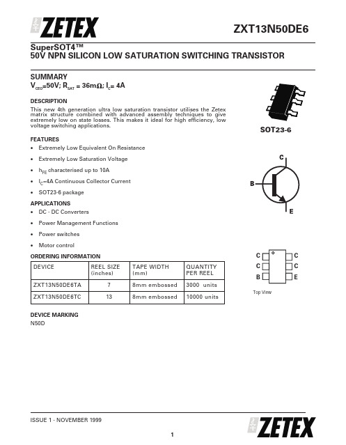
SuperSOT4™50V NPN SILICON LOW SATURATION SWITCHING TRANSISTORSUMMARYV CEO =50V; R SAT = 36m ;I C = 4ADESCRIPTIONThis new 4th generation ultra low saturation transistor utilises the Zetex matrix structure combined with advanced assembly techniques to give extremely low on state losses.This makes it ideal for high efficiency,low voltage switching applications.FEATURES •Extremely Low Equivalent On Resistance •Extremely Low Saturation Voltage •h FE characterised up to 10A •I C =4A Continuous Collector Current •SOT23-6 package APPLICATIONS•DC - DC Converters•Power Management Functions •Power switches •Motor controlORDERING INFORMATION DEVICEREEL SIZE (inches)TAPE WIDTH (mm)QUANTITY PER REELZXT13N50DE6TA 78mm embossed 3000units ZXT13N50DE6TC 138mm embossed10000unitsDEVICE MARKING N50DTop ViewSOT23-6C EBC C CTHERMAL RESISTANCEPARAMETERSYMBOL VALUE UNIT Junction to Ambient (a)R θJA 113°C/W Junction to Ambient (b)R θJA73°C/WNOTES(a) For a device surface mounted on 25mm x 25mm FR4 PCB with high coverage of single sided 1oz copper,in still air conditions(b) For a device surface mounted on FR4 PCB measured at t р5 secs.ABSOLUTE MAXIMUM RATINGS.PARAMETERSYMBOL LIMIT UNIT Collector-Base Voltage V CBO 100V Collector-Emitter Voltage V CEO 50V Emitter-Base Voltage V EBO 7.5V Peak Pulse CurrentI CM 10A Continuous Collector Current I C 4A Base CurrentI B 500mA Power Dissipation at TA=25°C (a)Linear Derating FactorP D 1.18.8W mW/°C Power Dissipation at TA=25°C (b)Linear Derating FactorP D 1.713.6W mW/°C Operating and Storage Temperature RangeT j :T stg-55 to +150°CELECTRICAL CHARACTERISTICS (at T amb= 25°C unless otherwise stated). PARAMETER SYMBOL MIN.TYP.MAX.UNIT CONDITIONS. Collector-Base BreakdownVoltageV(BR)CBO100190V I C=100ACollector-Emitter BreakdownVoltageV(BR)CEO5070V I C=10mA* Emitter-Base Breakdown Voltage V(BR)EBO7.58.5V I E=100A Collector Cut-Off Current I CBO100nA V CB=80V Emitter Cut-Off Current I EBO100nA V EB=6V Collector Emitter Cut-Off Current I CES100nA V CES=80VCollector-Emitter Saturation Voltage V CE(sat)8.07515017514512100200230180mVmVmVmVmVI C=0.1A,I B=10mA*I C=1A,I B=10mA*I C=3A,I B=50mA*I C=4A,I B=100mA*I C=4A,I B=400mA*Base-Emitter Saturation Voltage V BE(sat) 1.0V I C=4A,I B=100mA* Base-Emitter Turn-On Voltage V BE(on)0.9V I C=4A,V CE=2V*Static Forward Current Transfer Ratio h FE2503001001040045022030900I C=10mA,V CE=2V*I C=1A,V CE=2V*I C=4A,V CE=2V*I C=10A,V CE=2V*Transition Frequency f T115MHz I C=50mA,V CE10Vf=50MHzOutput Capacitance C obo31pF V CB=10V,f=1MHz Turn-On Time t(on)220ns V CC=10V,I C=1AI B1=I B2=20mA Turn-Off Time t(off)830ns*Measured under pulsed conditions. Pulse width=300µs. Duty cycle≤2%PACKAGE DIMENSIONSPAD LAYOUT DETAILSZetex plc.Fields New Road, Chadderton, Oldham, OL9-8NP, United Kingdom.Telephone: (44)161 622 4422 (Sales), (44)161 622 4444 (General Enquiries)Fax: (44)161 622 4420Zetex GmbHZetex Inc.Zetex (Asia) Ltd.These are supported by Streitfeldstraße 1947 Mall Drive, Unit 43510 Metroplaza, Tower 2agents and distributors in D-81673 München Commack NY 11725Hing Fong Road,major countries world-wide GermanyUSAKwai Fong, Hong Kong© Zetex plc 1999Telefon: (49) 89 45 49 49 0Telephone: (516) 543-7100Telephone:(852) 26100 611Fax: (49) 89 45 49 49 49Fax: (516) 864-7630Fax: (852) 24250 494Internet:This publication is issued to provide outline information only which (unless agreed by the Company in writing) may not be used, applied or reproduced for any purpose or form part of any order or contract or be regarded as a representation relating to the products or services concerned. The Company reservesthe right to alter without notice the specification, design, price or conditions of supply of any product or service.DIM MillimetresInches MinMax Min Max A 0.90 1.450.350.057A10.000.1500.006A20.90 1.300.0350.051b 0.350.500.0140.019C 0.090.200.00350.008D 2.80 3.000.1100.118E 2.60 3.000.1020.118E1 1.50 1.750.0590.069L 0.100.600.0040.002e 0.95REF 0.037REF e1 1.90REF0.074REFL0°10°0°10°。
ZXMP6A13FTA;中文规格书,Datasheet资料
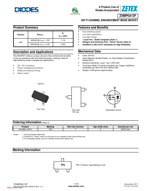
A Product Line ofDiodes IncorporatedZXMP6A13F60V P-CHANNEL ENHANCEMENT MODE MOSFETProduct SummaryV (BR)DSSR DS(on)I D T A = 25°C -60V400m Ω @ V GS = -10V -1.1A 600m Ω @ V GS = -4.5V-0.9ADescription and ApplicationsThis MOSFET utilizes a unique structure that combines the benefitsof low on-resistance with fast switching speed, making it ideal forhigh-efficiency power management applications.• DC - DC converters • Power management functions• Relay and solenoid driving• Motor controlFeatures and Benefits• Fast switching speed • Low input capacitance • Low gate charge• “Lead Free”, RoHS Compliant (Note 1)• Halogen and Antimony Free. "Green" Device (Note 2) • Qualified to AEC-Q101 Standards for High ReliabilityMechanical Data• Case: SOT23 • Case Material: Molded Plastic, UL Flammability Classification Rating 94V-0 • Moisture Sensitivity: Level 1 per J-STD-020 • Terminals: Matte Tin Finish annealed over Copper leadframeSolderable per MIL-STD-202, Method 208 • Weight: 0.008 grams (approximate)Ordering Information (Note 3)Product Marking Reel size (inches) Tape width (mm)Quantity per reel ZXMP6A13FTA7P6 7 8 3000UnitsNotes: 1. No purposefully added lead2. Diodes Inc's "Green" policy can be found on our website at .3. For packaging details, go to our website at .Marking InformationTop View Equivalent Circuit 7P6 = Product Type Marking CodeTop ViewPin Out D SG 7P6SOT23Maximum Ratings@T A = 25°C unless otherwise specifiedCharacteristic SymbolValueUnits Drain-Source Voltage V DSS-60 VGate-Source Voltage V GS±20 VContinuous Drain Current V GS = 10V(Note 5)T A = 70°C (Note 5)(Note 4)I D-1.1-0.8-0.9APulsed Drain Current (Note 6) I DM-4.0 A Continuous Source Current (Body Diode) (Note 5) I S-1.2 APulsed Source Current (Body Diode) (Note 6) I SM-4.0 AThermal Characteristics@T A = 25°C unless otherwise specifiedCharacteristic SymbolValueUnitPower Dissipation (Note 4)Linear Derating Factor P D 6255mWmW/°CPower Dissipation (Note 5)Linear Derating Factor P D 8066.5mWmW/°CThermal Resistance, Junction to Ambient (Note 4) RθJA200 °C/W Thermal Resistance, Junction to Ambient (Note 5) RθJA155 °C/W Operating and Storage Temperature Range T J, T STG-55 to +150 °CNotes: 4. For a device surface mounted on 25mm x 25mm FR4 PCB with high coverage of single sided 1oz copper, in still air conditions5. For a device surface mounted on FR4 PCB measured at t ≤ 5 secs.6. Repetitive rating 25mm x 25mm FR4 PCB, D = 0.05 pulse width =10μs - pulse current limited by maximum junction temperature.Thermal CharacteristicsSafe Operating Area204060801001201401600.00.10.20.30.40.50.60.7Derating CurveTemperature (°C)M a x P o w e r D i s s i p a t i o n (W )050100150200Transient Thermal ImpedanceT h e r m a l R es i s t a n c e (°C /W )Pulse Width (s)110Pulse Power DissipationPulse Width (s)M a x i m u m P o w e r (W )Electrical Characteristics @T A = 25°C unless otherwise specifiedCharacteristic Symbol Min Typ Max Unit Test ConditionOFF CHARACTERISTICSDrain-Source Breakdown Voltage BV DSS -60 ⎯ ⎯ V I D = -250μA, V GS = 0V Zero Gate Voltage Drain Current I DSS ⎯ ⎯ -0.5 μA V DS = -60V, V GS = 0V Gate-Source Leakage I GSS ⎯ ⎯ ±100 nA V GS = ±20V, V DS = 0V ON CHARACTERISTICS Gate Threshold Voltage V GS(th) -1.0 ⎯ -3.0 V I D = -250μA, V DS = V GSStatic Drain-Source On-Resistance (Note 7) R DS (ON) ⎯ ⎯0.400 Ω V GS = -10V, I D = -0.9A0.600 V GS = -4.5V, I D = -0.8AForward Transconductance (Notes 7 and 9) g fs ⎯ 1.8 ⎯ S V DS = -15V, I D = -0.9ADiode Forward Voltage (Note 7) V SD⎯ -0.85 -0.95 V T J = 25°C, I S = -0.8A, V GS = 0V Reverse Recovery Time (Note 9) t rr ⎯ 21.1 ⎯ ns T J = 25°C, I F = -0.9A,di/dt = 100A/μs Reverse Recovery Charge (Note 9) Q rr⎯ 19.3 ⎯ nC DYNAMIC CHARACTERISTICS (Note 9) Input Capacitance C iss⎯ 219 ⎯ pF V DS = -30V, V GS = 0Vf = 1.0MHzOutput Capacitance C oss⎯ 25.7 ⎯ Reverse Transfer Capacitance C rss ⎯ 20.5 ⎯ Turn-On Delay Time (Note 8) t D(on) ⎯ 1.6 ⎯ nsV DD = -30V, I D = -1A,R G ≅ 6.0Ω, V GS = -10V Turn-On Rise Time (Note 8) t r ⎯ 2.2 ⎯ Turn-Off Delay Time (Note 8) t D(off)⎯ 11.2 ⎯ Turn-Off Fall Time (Note 8) t f⎯ 5.7 ⎯ Total Gate Charge (Note 8) Q g⎯ 2.9 ⎯ nC V DS = -30V, V GS = -4.5V,I D = -0.9ATotal Gate Charge (Note 8) Q g ⎯ 5.9 ⎯nC V DS = -30V, V GS = -10V,I D = -0.9AGate-Source Charge (Note 8) Q gs ⎯ 0.74 ⎯Gate-Drain Charge (Note 8) Q gd ⎯ 1.5 ⎯Notes: 7. Measured under pulsed conditions. Pulse width = 300μs. Duty cycle ≤ 2%. 8. Switching characteristics are independent of operating junction temperature.9. For design aid only, not subject to production testing.Typical Characteristics0.11100.1110Output Characteristics-I D D r a i n C u r r e n t (A )-V DS Drain-Source Voltage (V)Output Characteristics-I D D r a i n C u r r e n t (A )-V DS Drain-Source Voltage (V)Normalised Curves v TemperatureN o r m a l i s e d R D S (o n ) a n d V G S (t h )Tj Junction Temperature (°C)On-Resistance v Drain Current R D S (o n -I D Drain Current (A)-I S D R e v e r s e D r a i n C u r r e n t (A )Typical Characteristics - continued-VDS- Drain - Source Voltage (V)Gate-Source Voltage v Gate Charge Capacitance v Drain-Source VoltageQ - Charge (nC)-VGSGate-SourceVoltage(V)Test CircuitsCurrentGate charge test circuitSwitching time test circuitBasic gate charge waveformSwitching time waveformsV DSGV GSVDDVDSPackage Outline DimensionsSuggested Pad LayoutSOT23Dim Min Max Typ A 0.37 0.51 0.40 B 1.20 1.40 1.30 C 2.30 2.50 2.40 D 0.89 1.03 0.915 F 0.45 0.60 0.535 G 1.78 2.05 1.83 H 2.80 3.00 2.90 J 0.0130.10 0.05 K 0.903 1.10 1.00 K1 - - 0.400 L 0.45 0.61 0.55 M 0.0850.18 0.11α0° 8° - All Dimensions in mmDimensions Value (in mm)Z 2.9 X 0.8 Y 0.9 C 2.0 E 1.35X EYCZIMPORTANT NOTICEDIODES INCORPORATED MAKES NO WARRANTY OF ANY KIND, EXPRESS OR IMPLIED, WITH REGARDING TO THIS DOCUMENT, INCLUDING, BUT NOT LIMITED TO, THE IMPLIED WARRANTIES OF MERCHANTABILITY AND FITNESS FOR A PARTICULAR PURPOSE (AND THEIR EQUIVALENTS UNDER THE LAWS OF ANY JURISDICTION).Diodes Incorporated and its subsidiaries reserve the right to make modifications, enhancements, improvements, corrections or other changes without further notice to this document and any product described herein. Diodes Incorporated does not assume any liability arising out of the application or use of this document or any product described herein; neither does Diodes Incorporated convey any license under its patent or trademark rights, nor the rights of others. Any Customer or user of this document or products described herein in such applications shall assume all risks of such use and will agree to hold Diodes Incorporated and all the companies whose products are represented on Diodes Incorporated website, harmless against all damages.Diodes Incorporated does not warrant or accept any liability whatsoever in respect of any products purchased through unauthorized sales channel. Should Customers purchase or use Diodes Incorporated products for any unintended or unauthorized application, Customers shall indemnify and hold Diodes Incorporated and its representatives harmless against all claims, damages, expenses, and attorney fees arising out of, directly or indirectly, any claim of personal injury or death associated with such unintended or unauthorized application.Products described herein may be covered by one or more United States, international or foreign patents pending. Product names and markings noted herein may also be covered by one or more United States, international or foreign trademarks.LIFE SUPPORTDiodes Incorporated products are specifically not authorized for use as critical components in life support devices or systems without the express written approval of the Chief Executive Officer of Diodes Incorporated. As used herein:A. Life support devices or systems are devices or systems which:1. are intended to implant into the body, or2. support or sustain life and whose failure to perform when properly used in accordance with instructions for use provided in thelabeling can be reasonably expected to result in significant injury to the user.B. A critical component is any component in a life support device or system whose failure to perform can be reasonably expected to cause the failure of the life support device or to affect its safety or effectiveness.Customers represent that they have all necessary expertise in the safety and regulatory ramifications of their life support devices or systems, and acknowledge and agree that they are solely responsible for all legal, regulatory and safety-related requirements concerning their products and any use of Diodes Incorporated products in such safety-critical, life support devices or systems, notwithstanding any devices- or systems-related information or support that may be provided by Diodes Incorporated. Further, Customers must fully indemnify Diodes Incorporated and its representatives against any damages arising out of the use of Diodes Incorporated products in such safety-critical, life support devices or systems.Copyright © 2011, Diodes Incorporated分销商库存信息: DIODESZXMP6A13FTA。
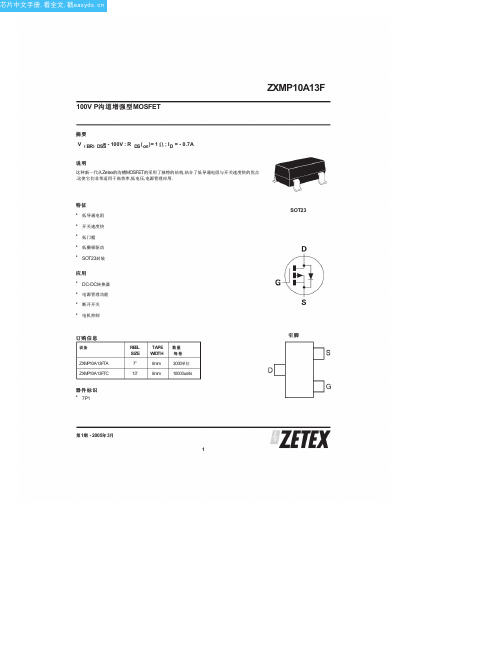
ZXMP10A13FTA中文资料(Diodes)中文数据手册「EasyDatasheet - 矽搜」
热阻
参数
结到环境
(a)
结到环境
(b)
符号
R JA R JA
VALUE 200 155
NOTES (a) For a device surface mounted on 25mm x 25mm FR4 PCB with high coverage of single sided 1oz copper, in still air conditions. (b) For a device surf ace mounted on FR4 PCB measured at t 5 sec. (c) Repetitive rating 25mm x 25mm FR4 PCB, D = 0.02, pulse width 300 s - pulse width limited by maximum junction temperature.
电气特性
ቤተ መጻሕፍቲ ባይዱ
参数
STATIC
漏源击穿电压
零栅压漏电流
门 - 体泄漏
门源阈值电压
静态漏源通态
抵抗性
(1)
正向跨
动态
(3)
输入电容
输出电容
反向传输电容
开关
(2) (3)
开启延迟时间
上升时间
关断延迟时间
下降时间
栅极电荷
总栅极电荷
栅极 - 源电荷
栅漏极电荷 源漏二极管 二极管的正向电压
反向恢复时间 反向恢复电荷
I D= -0.6A
3.5
nC
VDS = -50V, V GS= -10V
0.6
nC
I D= -0.6A
高速超导闪电跳变接收器(非镍金属、RoHS合规)产品包装尺寸说明书

BYG24DH to BYG24JH
200 to 600 140
20 at 1
1.5
1.5 at 1
150
x
1.5
1.15 at 1
150
x
AR3PDH to AR3PJH
x
200 to 1000 120 (140)
3
1.6 (1.9) at 3
175
AR3PKH to AR3PMH
x
SMPC (TO-277A) 4.75 x 6.65 x 1.2
VISH AY INTERTECHN OLOGY, INC.
AVALANCHE RECTIFIERS
Sinterglass and Plastic
Ultrafast Avalanche Rectifiers (Halogen-Free, RoHS-Compliant)
Product
BYT53A to BYT53G BYV26A to BYV26E BYV27-50 to BYV27-200
2
1.1 at 1
175
x
x
n/a
x
No
200 to 400 100
3.0
1.1 at 3
x
x
x
200 to 400 100
3
1.1 at 3
20 at 1
x
x
x
4.2 x Ø 4.3
200 to 1000 100 (150) 3 (2.9) 1.6 (1.78) at 3
50 to 1000 100
3
1.4 at 3
x
x
x
x
x
x
800 to 1000 250
MT7813规格书-中文 _Rev1.20(1)

描述MT7813是一款工作于零电流导通,峰值电流关断的临界导通模式(CRM ,Critical Conduction Mode )高精度LED 恒流控制芯片,主要应用于非隔离降压型LED 电源系统。
临界导通模式确保了MT7813可以控制功率开关在电感电流为零时刻开启,减小了功率管的开关损耗,确保了系统具有95%以上的峰值效率。
电感电流谷值为零的临界导通模式结合经过输入母线电压补偿后的峰值电感电流,确保了输出LED 电流的高精度,并且具有良好的线性调整率和负载调整率。
对电感量变化不敏感,可以使用工字电感,。
芯片内置高压功率MOS 管,外围电路简单,系统成本低。
MT7813工作电压宽,适合全范围交流输入电压或是10V —400V 直流电压输入。
MT7813同时实现了各种保护功能,包括逐周期过流保护(OCP )、LED 短路保护(SCP )、LED 开路保护(OVP )和过热保护(OTP )等,以确保系统可靠地工作。
∙ 临界导通模式,对电感不敏感 ∙ 最高95%以上的峰值效率 ∙ 高精度LED 恒流电流 ∙ 逐周期峰值电流控制 ∙ LED 短路保护 ∙ LED 开路保护 ∙ 前沿消隐控制 ∙ 欠压锁定保护(UVLO) ∙ 过温保护 ∙SOP8 / DIP8封装应用∙ LED 球泡灯,日光灯,信号灯,景观灯等 ∙ LED 舞台灯,蜡烛灯,玉米灯等 ∙其他LED 驱动应用及通用恒流源典型应用电路极限参数推荐工作条件管脚排列图管脚描述电气参数原理框图 SWCSVOVP GNDDRAIN功能描述MT7813是一款内置高压功率管的恒流驱动的芯片,适用于LED 照明驱动。
芯片工作于电感电流临界导通模式,控制功率开关在电感电流为零时刻开启,减小了功率管的开关损耗,提高了效率。
采用MT7813芯片的驱动电路恒流精度高,外围元器件少,成本低。
启动过程上电时,VCC 通过一个连接到输入母线的启动电阻充电。
当VCC 达到12V 时,控制逻辑就开始工作,内部开关开始开关动作。
EL31116CN EL31216CN EL31316CN EL31416CN 用户手册说明书

用户手册EL31116CN/EL31216CN/ EL31316CN/EL31416CN 数字无绳电话机无绳电话机欢迎欢迎购买 AT&T 产品。
在使用此 AT&T 产品前,请仔细阅读用户手册中第 53 至 54 页的重要安全信息。
为了更容易地安装和使用您的电话,也请仔细阅读用户手册中所有操作说明和常见问题的帮助信息。
您也可以浏览我们的网站或致电服务热线。
网站:服务热线:400-022-9929请保管好销货收据,以便在享受质保服务时作为相关证明。
产品名称: 数字无绳电话机中国专用型号:HWDCD2310(3)P/TSD企业型号: EL31116CN/EL31216CN/EL31316CN/EL31416CN© 2017-2018 伟易达通讯设备有限公司保留所有权利。
此使用手冊上所载述的 AT&T 商标及 AT&T 图标为 AT&T 拥有的商号,并在 AT&T 的品牌许可协议下授权予香港伟易达通讯设备有限公司使用。
中国印刷。
部件清单请保管好销货收据, 以便在享受质保服务时作为相关证明。
EL31116CN/EL31216CN/EL31316CN/EL31416CN 的包装盒中包括以下物品:无绳子机充电器(EL31116不含充电器)电话线主机电源适配器AAA 镍氢可充电电池无绳子机用户手册座机保修卡电池盖用戶手冊EL31116CN/EL31216CN/ EL31316CN/EL31416CN 2.4GHz 数字无绳电话机目录安装 (1)快速使用指南.-.子机 (2)快速使用指南.-.座机 (5)座机和充电座安装 (6)安装座机 (6)安装充电座 (6)安装电池和充电 (7)电话设置 (9)无绳子机设置 (10)设置日期 / 时间 (10)铃声音量 (12)内线通话的响铃音调 (12)外线通话的铃声音调 (13)闹钟设置 (13)重命名子机 (15)按键音 (16)电池提示音 (16)待机状态下的屏幕显示 (17)自动应答 (18)重设子机 (18)座机设置(使用无绳子机) (19)铃声音量 (19)铃声音调 (19)拨号模式 (20)闪断时间 (20)IP 号码 (21)更改 PIN 码 (22)电话操作 (23)拨打电话 (23)挂机拨号(预拨号) (23)接听来电 (23)结束通话 (23)免提通话 (24)安静模式 (24)重拨上次的号码 (25)通话时的操作 (26)音量控制 (26)静音 (26)内线通话 (27)拨打内线电话 (27)转移外线通话 (28)进行三方通话 (29)电话簿 (30)容量 (30)新增电话簿记录 (30)拨号键 (31)查看电话簿记录 (32)按姓名搜索 (33)搜索电话簿 (33)拨打、编辑或删除电话.簿记录 (34)显示拨号 (34)删除一个电话簿记录 (34)编辑电话簿记录 (35)删除所有电话簿记录 (36)查看电话簿使用情况 (36)来电显示 (37)来电显示操作 (38)查看来电清单 (38)查看来电清单记录的详细信息 (38)拨打来电清单的记录 (39)删除一个来电清单记录 (39)删除所有来电清单记录 (39)储存来电显示清单号码至电话簿 (40)来电信息缺失的原因 (41)增加及登记新子机 (42)登记子机到座机 (42)解除子机登记 (43)解除子机登记 (43)屏幕图标和提示音 (44)子机屏幕图标 (44)子机提示音 (45)常见问题 (46)维护 (52)重要安全信息 (53)安全信息 (53)特别注意 (54)产品中有毒有害物质或.元素的名称及含量表 (55)产品技术参数 (57)2.4GHz FHSS军用跳频扩频数字无绳通讯技术 (57)电话操作范围 (57)安装在电话线墙壁插口和非开关控制的电源插座附近安装您的座机。
Z515中文资料(Intel)中文数据手册「EasyDatasheet - 矽搜」
UNLESS O THERW ISE AGREED IN W RITING BY INTEL, THE INTEL PRO DUCTS ARE NO T DESIGNED NO R INTENDED FO R ANY APPLICATIO N IN W HICH THE FAILURE O F THE INTEL PRO DUCT CO ULD CREATE A SITUATIO N W HERE PERSO NAL INJURY O R DEATH MAY O CCUR.
Contact your local Intel sales office or your distributor to obtain the latest specifications and before placing your product order. Copie s of docum ents which have an orde r num be r and are re fere nce d in this docum ent, or othe r Inte l lite rature , m ay be obtaine d
RZC2013-中文规格书-1.0

Version:1.0
https:///?spm=a261y.7663282.0.0.I3f0wy
RZC2013
2A,27V 同步降压型电源管理 EN 关断阈值迟滞 EN 锁定阈值电压 EN 锁定阈值电压 反馈部分 反馈基准电压 过压保护基准电压 软启动部分 软启动电流 软启动周期 误差放大部分 差分放大器电压 差分放大器跨导 过温部分 TOTP_R 过温保护 TOTP_F 过温保护迟滞 MOS 部分 高端开关导通阻抗 低端开关导通阻抗 高端开关漏电流 高端开关电流限制 低端开关电流限制 RDS(ON)-1 RDS(ON)-2 VEN =0V,VSW =0V 最大占空比 从漏极到源极 2.4 3.4 1.1 130 130 10 mΩ mΩ uA A A TOTP_HYS 温度下降 110 40 ℃ ℃ 温度上升 150 ℃ AEA GEA △IC =±10uA 480 800 V/V uA/ V VSS =0V CSS =0.1uF 6 15 uA mS VFB VFB_OVP 4.75 ≦VIN≦27V 0.900 0.925 1.1 0.950 V V 2.2 200 2.5 200 2.7 mV V mV
电感
电感作为储能器件,与输出电容一同构成 LC 滤波电路,故电感选择不当会造成带载能 力不足、输出纹波大、转换效率低等问题,故电感选择也是相当重要的。电感量越小,电源 系统的动态响应就越好, 但是输出纹波和带载能力可能会受影响。 可根据下面的公式快速选 择电源系统所需的电感感量。
L
(VIN VOUT ) VOUT VIN FOC I OUT K
RZC2013
2A,27V 同步降压型电源管理
产品概述
RZC2013 是一体的同步降压型电源管理集成电路, 内置 2 个导通电阻为 130 mΩ 的 MOS, 可提供 2A 的连续电流,输入电压范围为 4.75V 到 27V。电流模式控制提供快速动态响应和 逐周期的电流限制。 RZC2013 具有可调节的软启动防止在开通瞬间的浪涌电流损坏器件, 在关断模式下电源 电流降至 1uA。 RZC2013 采用 SOP-8 和 ESOP-8 两种封装,封装体积小,外围器件少,使用于小体积的 电源应用方案中。
- 1、下载文档前请自行甄别文档内容的完整性,平台不提供额外的编辑、内容补充、找答案等附加服务。
- 2、"仅部分预览"的文档,不可在线预览部分如存在完整性等问题,可反馈申请退款(可完整预览的文档不适用该条件!)。
- 3、如文档侵犯您的权益,请联系客服反馈,我们会尽快为您处理(人工客服工作时间:9:00-18:30)。
SuperSOT4™20V PNP SILICON LOW SATURATION SWITCHING TRANSISTORSUMMARYV CEO =-20V; R SAT = 47m ;I C = -3.5ADESCRIPTIONThis new 4th generation ultra low saturation transistor utilises the Zetex matrix structure combined with advanced assembly techniques to give extremely low on state losses.This makes it ideal for high efficiency,low voltage switching applications.FEATURES •Extremely Low Equivalent On Resistance •Extremely Low Saturation Voltage •h FE characterised up to 10A•I C =3.5A Continuous Collector Current •SOT23-6 package APPLICATIONS•DC - DC Converters•Power Management Functions •Power switches •Motor controlORDERING INFORMATION DEVICEREEL SIZE (inches)TAPE WIDTH (mm)QUANTITY PER REEL ZXT13P20DE6TA 78mm embossed 3000units ZXT13P20DE6TC 138mm embossed10000unitsDEVICE MARKING P20DTop ViewSOT23-6C EBC C CTHERMAL RESISTANCEPARAMETERSYMBOL VALUE UNIT Junction to Ambient (a)R θJA 113°C/W Junction to Ambient (b)R θJA73°C/WNOTES(a) For a device surface mounted on 25mm x 25mm FR4 PCB with high coverage of single sided 1oz copper,in still air conditions(b) For a device surface mounted on FR4 PCB measured at t р5 secs.ABSOLUTE MAXIMUM RATINGS.PARAMETERSYMBOL LIMIT UNIT Collector-Base Voltage V CBO -25V Collector-Emitter Voltage V CEO -20V Emitter-Base Voltage V EBO -7.5V Peak Pulse CurrentI CM -10A Continuous Collector Current I C -4A Base CurrentI B -500mA Power Dissipation at TA=25°C (a)Linear Derating FactorP D 1.18.8W mW/°C Power Dissipation at TA=25°C (b)Linear Derating FactorP D 1.713.6W mW/°C Operating and Storage Temperature RangeT j :T stg-55 to +150°CELECTRICAL CHARACTERISTICS (at T amb= 25°C unless otherwise stated). PARAMETER SYMBOL MIN.TYP.MAX.UNIT CONDITIONS. Collector-Base BreakdownVoltageV(BR)CBO-25-55V I C=-100ACollector-Emitter BreakdownVoltageV(BR)CEO-20-50V I C=-10mA* Emitter-Base Breakdown Voltage V(BR)EBO-7.5-8.5V I E=-100A Collector Cut-Off Current I CBO-100nA V CB=-20V Emitter Cut-Off Current I EBO-100nA V EB=-6V Collector Emitter Cut-Off Current I CES-100nA V CES=-20VCollector-Emitter Saturation Voltage V CE(sat)-10-100-165-15-130-250mVmVmVI C=-0.1A,I B=-10mA*I C=-1A,I B=-10mA*I C=-3.5A,I B=-350mA*Base-Emitter Saturation Voltage V BE(sat)-1.1V I C=-3.5A,I B=-350mA* Base-Emitter Turn-On Voltage V BE(on)-0.9V I C=-3.5A,V CE=-2V*Static Forward Current Transfer Ratio h FE3003002002050045030030900I C=-10mA,V CE=-2V*I C=-1A,V CE=-2V*I C=-4A,V CE=-2V*I C=-10A,V CE=-2V*Transition Frequency f T90MHz I C=-50mA,V CE=-10Vf=50MHzOutput Capacitance C obo62pF V CB=-10V,f=1MHz Turn-On Time t(on)95ns V CC=-10V,I C=-2AI B1=I B2=-40mATurn-Off Time t(off)395ns*Measured under pulsed conditions. Pulse width=300µs. Duty cycle≤2%PACKAGE DIMENSIONSPAD LAYOUT DETAILSZetex plc.Fields New Road, Chadderton, Oldham, OL9-8NP, United Kingdom.Telephone: (44)161 622 4422 (Sales), (44)161 622 4444 (General Enquiries)Fax: (44)161 622 4420Zetex GmbHZetex Inc.Zetex (Asia) Ltd.These are supported by Streitfeldstraße 1947 Mall Drive, Unit 43510 Metroplaza, Tower 2agents and distributors in D-81673 München Commack NY 11725Hing Fong Road,major countries world-wide GermanyUSAKwai Fong, Hong Kong© Zetex plc 1999Telefon: (49) 89 45 49 49 0Telephone: (631) 543-7100Telephone:(852) 26100 611Fax: (49) 89 45 49 49 49Fax: (631) 864-7630Fax: (852) 24250 494Internet:This publication is issued to provide outline information only which (unless agreed by the Company in writing) may not be used, applied or reproduced for any purpose or form part of any order or contract or be regarded as a representation relating to the products or services concerned. The Company reservesthe right to alter without notice the specification, design, price or conditions of supply of any product or service.DIM MillimetresInches MinMax Min Max A 0.90 1.450.350.057A10.000.1500.006A20.90 1.300.0350.051b 0.350.500.0140.019C 0.090.200.00350.008D 2.80 3.000.1100.118E 2.60 3.000.1020.118E1 1.50 1.750.0590.069L 0.100.600.0040.002e 0.95REF 0.037REF e1 1.90REF0.074REFL0°10°0°10°分销商库存信息:DIODESZXT13P20DE6TA ZXT13P20DE6TC。