HER0808G中文资料
塑封高效率整流二极管参数HER101--HER108

40
30
20
10
0 1 2 4 6 10 20 40 100 通过电流的周期 Number of Cycles at 60 Hz.
平均正向电流 IF(AV) (A) IF(A) Average Forward Rectified Current (A)
HER101 ...... HER108
正向电流降额曲线 FORWARD CURRENT DERATING CURVE 1.4
10mm 10mm
1.2
1
0.8
0.6
0.4
0.2 0 0 25 50 75 100 125 150 175 环境温度 Ta(°C) Tamb, ambient temperature (°C)
峰值正向浪涌电流 IFSM(A) IFSM Peak Forward Surge Current (A)
大昌电子 DACHANG ELECTRONICS
HER103
1
HER104, HER105
0.2
HER106 thru
0.1
HER108
Tj = 25 °C
0.01 0.6 0.8 1 1.2 1.4 1.6 正向电压 VF(V) VF Instantaneous Forward Voltage (V)
浪涌特性曲线(最大值) MAXIMUM NON REPETITIVE PEAK FORWARD SURGE CURRENT 50
HER 108
最大可重复峰值反向电压 Maximum repetitive peak reverse voltage
VRRM
50 100 200 300 400 600 800 1000
最大均方根电压 Maximum RMS voltage
MKH 8070 说明书
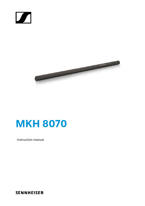
MKH 8070 Instruction manualImportant safety instructions Important safety instructions1.Read these safety instructions and the instruction manual of the product.2.Keep these safety instructions and the instruction manual of the product.Always include all instructions when passing the product on to third parties.3.Only use attachments, accessories and spare parts specified by the manu-facturer.4.Caution: The protective basket and pop shield must be completely dry whenyou mount them on the microphone. Moisture can cause malfunctions or damage to the capsule.5.Connect the microphone only to microphone inputs and supply units thatprovide 48 V phantom powering in accordance with IEC 61938.6.Do not attempt to open the product housing on your own. The warranty isvoided for products opened by the customer.7.Refer all servicing to qualified service personnel. Servicing is requiredwhen the product has been damaged in any way, liquid has been spilled or objects have fallen into the product, when the product has been exposed to rain or moisture, does not operate normally, or has been dropped.e the product only under the conditions of use listed in the specifications.9.Let the product come to ambient temperature before switching it on.10.Do not operate the product if it was damaged during transportation.11.Always run cables so that no one can trip over them.12.Keep the product and its connections away from liquids and electricallyconductive objects that are not necessary for operating the product.13.Do not use any solvents or aggressive cleaning agents to clean the product.14.Caution: Very high signal levels can damage your hearing and your loud-speakers. Reduce the volume on the connected audio devices beforeswitching on the product; this will also help prevent acoustic feedback. Intended useThe product is designed for indoor use.It is considered improper use when the product is used for any application not named in the corresponding instruction manual.Sennheiser does not accept liability for damage arising from improper use or misuse of this product and its attachments/accessories.Before putting the products into operation, please observe the respective country-specific regulations!MKH 8070Delivery includesDelivery includes•Microphone, consisting of the MKH 8070 microphone head and the MZX 8000 XLR module•MZQ 8070 microphone clamp•MZW 8070 foam windshield•Instruction manual•Frequency response sheet•Threaded transport tubeProduct overview1 Foam windshield2 Microphone head3 XLR module4 Microphone clamp (thread adaptor included for 3/8" and 5/8" threads) MKH 8070Putting the MKH 8070 into operation Putting the MKH 8070 into operation Connecting the microphoneConnection data of the MKH 8070:•48 V ± 4 V phantom powering (P48, as per IEC 61938)•XLR-3 connector, balancedTo connect the MKH 8070 to a mixing console or recording device:f Connect the socket of the microphone cable to the microphone.f Connect the connector of the microphone cable to the mixing console orrecording device.Attaching the microphonef Select the suitable mounting thread:•Without thread insert: 5/8" thread•Thread insert: 3/8" threadf Screw the microphone clamp 4 to a stand.f Place the microphone with its back end into the microphone clamp: Makesure that the lateral slots are not covered.f Orient the microphone together with the microphone clamp and fix them byscrewing the wing screw tight.MKH 8070Using optional modulesTo suppress structure-borne noise, you can use the optional shock mount.Sennheiser MZS 20-1Using the windshieldThe windshield changes the sound only slightly, but attenuates wind noise by approx. 25 dB.f Place the MZW 8070 foam windshield 1 over the microphone head 2 so thatall lateral slots are covered.Alternative windshields are available as accessories and can be found on the MKH 8070 product page at .Using optional modulesYou can retrofit and extend the microphones of the modular MKH 8000 micro-phone series by using optional modules.The MZF 8000 II filter moduleThe MZF 8000 II filter module has been specially designed for broadcast and film applications. It effectively filters out interference caused by infrasound, such a lowfrequency wind and handling noise.f If necessary, disconnect a connected XLR cable in order to not distort thecable and to avoid short-circuits.MKH 8070Transporting the microphone f Unscrew the microphone head 2 from the XLR module 3.f Screw the MZF 8000 II filter module 4 at a suitable place in the audio signalTransporting the microphonef Let the microphone dry if you used it under extreme climatic conditions.f If necessary, remove the windshield or take the microphone out of the basketwindshield.f Slide the microphone into the transport tube.MKH 8070Cleaning and maintaining the microphoneCleaning and maintaining the microphoneCAUTIONDAMAGE TO THE PRODUCT DUE TO LIQUIDS!Liquids entering the product can short-circuit the electronics or damage the mechanics. Solvents or cleansing agents can damage the surface of the prod-uct.f Keep all liquids away from the product.f Only use a soft, slightly damp cloth to clean the product. SpecificationsPick-up pattern lobarFrequency response45 Hz to 20,000 HzSensitivity-19 dBV/Pa (112 mV/Pa)Max. sound pressure level124 dB SPLEquivalent noise level8 dB(A) (DIN-IEC 651)21 dB (CCIR 268-3)Nominal impedance25 ΩMin. terminating impedance 2 kΩPhantom powering48 V ± 4 V (P48, IEC 61938)Current consumption3,3 mADiameter19 mmLengthwith MZX 8000 XLR module 432 mm 465 mWeightwith MZX 8000 XLR module 300 g 332 gOperating temperature-10 °C to +60 °CMKH 8070MKH 8070SpecificationsPolar pattern30°150°120°60°90°0510152025dB30°0°180°150°120°60°90°125 Hz 250 Hz 500 Hz 1,000 Hz2,000 Hz 4,000 Hz 8,000 Hz 16,000 HzFrequency response-10-20-30-40-50-60dB 90°0°50 H z100 H z200 H z500 H z1 k H z2 k H z5 k H z10 k H z20 k H zManufacturer declarationsManufacturer declarationsWarrantySennheiser electronic GmbH & Co. KG gives a warranty of 24 months on these products.For the current warranty conditions, please visit our website at or contact your Sennheiser partner.Warranty FOR AUSTRALIA and NEW ZEALAND ONLY:Sennheiser Australia Pty Ltd provides a warranty of 24 months on these prod-ucts.For the current warranty conditions, visit Sennheiser website:Australia: https:///New Zealand: https:///Sennheiser goods come with guarantees that cannot be excluded under Aus-tralian and New Zealand Consumer law. You are entitled to a replacement or refund for a major failure and compensation for any other reasonably fore-seeable loss or damage. You are also entitled to have the goods repaired or replaced if the goods fail to be of acceptable quality and the failure does not amount to a major failure.This warranty is in addition to other rights or remedies under law. Nothing in this warranty excludes, limits or modifies any remedy available to be consumer which is granted by law.To make a claim under this contract, raise a case via Sennheiser website Australia: https:///service-support-contactNew Zealand: https:///service-support-contactAll expenses of claiming the warranty will be borne by the person making the claim.Sennheiser international warranty is provided by: Sennheiser Australia Pty Ltd (ABN 68 165 388 312) Level 14, Tower A Zenith Building, 821 Pacific Highway, Chatswood NSW 2067, AustraliaIn compliance with the following requirementsEU: WEEE Directive (2012/19/EU)UK: WEEE Regulations (2013)Notes on disposalThe symbol of the crossed-out dumpster on the product, the (rechargeable) battery (if applicable) and/or the packaging indicates that these products must MKH 8070Manufacturer declarations not be disposed of with normal household waste, but must be disposed of sep-arately at the end of their service life. For the packaging, follow the regulations in your country for separating waste. Improper disposal of packaging materials can be harmful to your health and the environment.The separate collection of waste electrical and electronic equipment, (re-chargeable) batteries (if applicable) and packaging is intended to promote reuse and recycling and to prevent negative impacts on public health and the environment, for example due to hazardous substances contained in these products. At the end of their service life, recycle electrical and electronic equipment and (rechargeable) batteries so that their materials can be reused and to prevent environmental pollution.If (rechargeable) batteries can be removed without destroying them, you are obliged to dispose of them separately (see the product’s operating instructions for information on how to remove the batteries safely). Be especially careful when handling (rechargeable) batteries containing lithium, as these pose spe-cial hazards, such as the risk of fire and/or health risks if button cells are swal-lowed. Reduce battery waste as much as possible by using longer-life batteries or rechargeable batteries.Further information on the recycling of these products can be obtained from your municipal administration, from the municipal collection points, or from your Sennheiser partner. You may also be able to return electrical or electronic equipment to your distributor, if they are legally required to do so. By dispos-ing of your batteries properly, you are helping to protect public health and the environment.EU Declaration of conformity•RoHS Directive (2011/65/EU)•EMC Directive (2014/30/EU)UK Declaration of conformity•RoHS Regulations (2012)•EMC Regulations (2016)The full text of the EU declaration of conformity is available at the following internet address: /download.Statements regarding the FCC and Industry Canada rulesThis device complies with part 15 of the FCC rules. Operation is subject to the following two conditions: (1) this device may not cause harmful interference, and (2) this device must accept any interference received, including interfer-ence that may cause undesired operation.MKH 8070Compliance ComplianceEurope EN 55032EN 55035UKUSA FCC 47 CFR 15 subpart BCanada Industry Canada ICES_003ChinaAustralia/New ZealandMKH 8070Sennheiser electronic GmbH & Co. KGAm Labor 1, 30900 Wedemark, Germany, Printed in Germany, Publ. 07/23, 581395/A04。
TA880GB HD TA890GXB HD设置手册

TA880GB HD & TA890GXB HD 设置手册
防静电操作规则
静电可能严重损坏您的设备,在处理主板以及其它的系统设备的时候要特别注意, 避免和主板上的系统组件的不必要接触,保证在抗静电的环境下工作,避免静电 放电可能对主板造成损坏,当在您的机箱中插入或者移除设备时,请保证电源处 于断开状态,厂商对于不遵照本操作规则或者不遵守安全规范而对主板造成的损 坏不负责。
2.2
风扇接头 .............................................................................................6
2.3
系统内存 .............................................................................................7
5.3
RAID 运行.........................................................................................19
第六章: T 系列 BIOS 和软件 ......................................... 22
2.4
接口和插槽 .........................................................................................9
第三章:接头和跳线安装 .............................................. 12
1.2 附件
Heraeus Megafuge 8系列台式离心机

Thermo ScientificHeraeus Megafuge 8 系列台式离心机适心所用成就卓越新!Thermo Scientific™Heraeus™ Megafuge™ 8 & 8R 紧凑型台式离心机适心所用高度的可靠性,保障实验结果的一致性创新的Thermo Scientific离心技术合乎您所预期,满足您最急迫所需的实验室离心应用,兼顾未来之需通风型(左)和冷冻型(右)Auto-lock™ 转头自锁按钮式自锁系统,实现多样的应用及操作的方便性和安全性ClickSeal™ 防生物污染转头盖可单手操作,其生物安全性经过第三方权威认证成就卓越同类型号中最好的离心处理能力可离心 8×50 mL尖底管、24×5/7 mL 采血管、酶标板及微量管,一台仪器实现所有功能多种角转头选择,性能优异离心50 mL尖底管离心力可达12,000×g;离心多种微量离心管离心力可达30,279×g经过第三方HPA,(Porton Down, UK)生物安全认证适心所用成就卓越简单的解决方案灵活的样品处理能力按钮式转头自锁系统在3秒内实现转头更换及安全锁定,带来诸多好处:安全无忧地进行转头安装及拆卸如包可靠的质量安全的操作■可选择生物安全离心附件,包括第三方权威认证的 ClickSeal防生物污染密封盖,实现带着手套、单手操作1. 生物安全性通过2.详细信息见样品处理简便用户友好■一键式便捷程序键,可预设程序■高清晰背光显示屏,便于观察实验参数■可选择运行结束提示功能,包括腔盖自动开启、显示器全屏闪烁、音量可调的声音报警等■高灵敏按键,可戴手套进行操作,并可抵御多种清洁剂,便于清洁■多语种 – 英、德、法、丹麦、意、俄、西班牙 – 显示程序、运行状态、报警及维修信息等结构紧凑的型号、优异的离心容量、操作便捷的智能控制面板可用字母及数字命名程序,可多达12字节,方便程序的识别及选择可选择“只使用程序模式”,适用于使用权限管理适心所用 临床应用 成就卓越水平转头一次可离心24×5/7 mL 采血管Auto-Lock 转头自锁系统方便操作及日常维护符合最新的临床及质量安全标准加减速快,节省离心时间用于日常临床应用的专用转头TX-100S 临床水平转头,带密封载架带防生物污染密封盖的状态下离心 8TX-100临床水平转头,带开放载架一次可离心16 根采血管M10酶标板转头8 x 50 mL 分立式密封角转头CLINIConic角转头Hematocrit 血比容转头通风型4,500 rpm 3,260×g 冷冻型4,500 rpm3,260×g通风型4,500 rpm3,260×g冷冻型4,500 rpm3,260×g• 更快的离心•提高的分离效果• 实现更多的应用领域除此之外,Auto-Lock方便地更换其它转头的便利性用于科研应用的转头HIGHConic III 角转头微量角转头1通过PHA, Porton Down, UK 第三方生物安全认证多样的转头选择提供应用的广泛性临床水平转头HIGHConic III转头容量离心管规格MicroClick 24×2微量角转头MicroClick 30×2微量角转头8×Hematocrit 血比容转头Thermo Scientific Heraeus Megafuge 8系列离心机技术参数Heraeus Megafuge 8RHeraeus Megafuge 81通过HPA Porton Down, UK第三方生物安全认证适心所用成就卓越适心所用更多的离心机选择完美的配合从1升离心瓶,到15 / 50 mL尖底管以及酶标板,Thermo Scientific Nalgene™ 和 Nunc™ 均能提供高品质的离心耗材,与离心机及相关转头形成完美的搭配,实现无与伦比的离心体验。
无源器件资料

2.1 无源器件基础知识 (3)工程常用无源器件 (3)无源器件的生产工艺要求 (6)光器件基本知识 (6)微带与腔体的区别 (8)2.2 常用器件分类介绍 (8)微带功率分配器 (8)器件特点 (8)器件用途 (8)器件型号及指标 (9)微带定向耦合器 (12)器件特点 (12)器件用途 (13)器件型号及指标 (13)腔体耦合器 (16)器件特点 (16)器件用途 (17)器件型号及指标 (17)基站耦合器 (40)器件特点 (40)器件用途 (41)器件型号及指标 (41)双频合路器 (48)器件特点 (48)器件用途 (49)器件型号及指标 (49)腔体功率分配器 (51)器件特点 (51)器件用途 (52)器件型号及指标 (52)电桥 (55)器件特点 (55)器件用途 (56)器件型号及指标 (56)腔体双工器 (58)器件特点 (58)器件用途 (59)器件型号及指标 (59)腔体滤波器 (68)器件特点 (68)器件用途 (69)器件型号及指标 (69)光器件 (85)固定光衰减器 (85)光环形器 (86)光隔离器 (87)光纤光缆跳线 (88)单/双窗口宽带耦合器(1*2、2*2 系列) (89)高隔离度波分复用器 (91)滤波片型波分复用器 (92)天线 ........................................................................................ 错误!未定义书签。
天线理论知识 ....................................................................... 错误!未定义书签。
天线的选择原则................................................................... 错误!未定义书签。
ABOV半导体 MC80F0708 0704 MC80F0808 0804 8位单片机 中文手册

A BO V半导体有限公司8位单片机MC80F0708/0704MC80F0808/0804中文手册(1.01版)2008.6ABOV semiconductorwww.abov.co.krMC80F0708/0808修订记录1.01版(6.3.2008)本册修改内部晶振规范1.0版(2.27.2008)在7.4A/D转换特性中增加最小电压参数AV REF。
在7.6典型特征中增加了特性图。
0.5版(9.28.2007)修正8bit计数器说明及图表中的错误。
0.4版(5.5.2007)在1~4MHz,增加操作范围在2.2V~5.5V内。
修正图9-2中的错误:更改R04,R07和PSR1的EC0,EC1为R05,R06和T0O,T2O。
0.3版 (5.2.2007)增加28 QFNP封装。
0.21版(5.2007)增加了T VDD参数规格并且改变了T POR的直流电器特性。
配置选项加入了注释,并对勘误表进行了修正。
0.1版 (8.2006)最初版本1.0版出版发行F A E Tea m©2006A BO V s e m ic ondu c t o r L t d.A ll r ig h t r e s e r v e d.本手册的其它资料由ABOV半导体有限公司韩国办公室或者销售商和代理人提供。
ABOV半导体保留更改数据的权利,并不再另行通知。
这个手册的资料,图表和其它数据都是正确可靠的,但是ABOV半导体没有责任阻止违反专利权或其它权利的个人和团体使用本手册。
注意:本文乃英文版中文翻译,中文文本如有歧义,概以英文为准。
MC80F0708/08081. 概述.............................................................................................................. 描述................................................................................................................. 特性................................................................................................................. 开发工具.......................................................................................................... 订购须知..........................................................................................................2. 系统方框图.....................................................................................................3. 引脚分配.......................................................................................................4. 封装尺寸.......................................................................................................5. 引脚功能.......................................................................................................6. 端口结构.......................................................................................................7. 电器特性.......................................................................................................极限参数.......................................................................................................... 推荐操作参数................................................................................................... A/D转换特性.................................................................................................... DC电器特性.................................................................................................. AC特性............................................................................................................ 典型特性..........................................................................................................8. 存储器结构..................................................................................................... 寄存器.............................................................................................................. 程序存储器........................................................................................................ 数据存储器........................................................................................................ 寻址方式............................................................................................................9. I/O 口............................................................................................................ R0 和R0IO 寄存器........................................................................................... R1 和R1IO 寄存器........................................................................................... R2 和 R2IO 寄存器…………………………………………………………………. R3 和R3IO 寄存器...........................................................................................10. 时钟发生器................................................................................................... 振荡电路..........................................................................................................11. 基本间隔定时器............................................................................................12. 看门狗定时器..............................................................................................13. 定时器/事件计数器....................................................................................... 8位定时/计数器方式....................................................................................... 16位定时/计数器方式...................................................................................... 8位(16位) 比较输出....................................................................................... 8位捕捉方式................................................................................................... 16位捕捉方式.................................................................................................. PWM 方式.........................................................................................................14. 模数转换器...................................................................................................15. 串行输入/输出口(SIO)…………………………………………………………... 发送/接受定时……………………………………………………………………...... 串行I/O的使用………………………………………………………………………..16.蜂鸣器功能…………………………………………………………………………17. 中断............................................................................................................1 1 1 3 4 5 6 7 10 12 16 16 16 16 16 17 18 19 22 22 26 28 33 37 37 40 41 42 42 44 46 49 52 57 58 59 63 66 70 73 74 76 77 79MC80F0708/0808中断优先级 (81)BRK 中断 (83)中断嵌套 (83)外部中断 (85)18. 节电模式操作 (87)Sleep模式 (87)Stop模式 (88)Stop模式(内部RC-振荡看门狗定时器方式) (91)最小消耗电流 (93)19.复位 (95)20.电源失效处理 (97)21.抗干扰措施 (99)振荡噪声保护 (99)振荡失效处理 (100)22.器件配置区 (101)23.仿真器EV A.板安装 (102)A. 指令图 (i)B. 指令集 (ii)MC80F0708/0808 MC80F0708/0704MC80F0808/08041、概述1.1、描述CMOS8位单片机10位A/D转换器MC80F0708(4)/0808(4)是拥有8K(4K)字节FLASH(MTP)程序存储器的CMOS8位单片机。
FortiGate-80D 产品说明书

Multi-threat protection from a single device increases security and lowers costs Unlimited user licensing and comprehensive features Allows implementation of WAN optimization and web cache, as well as extensive internal logging and reporting.
FortiCare
Worldwide 24x7 Support
FortiGuard
Threat Research & Response
HaБайду номын сангаасdware
5
5
5
1
2
3
1 Console Port
Advanced Features
The FortiGate-80D offers beyond the industry’s best firewall with the latest in Advanced Threat Protection including Sandboxing and anti-bot protection, Feature Select Options for simplifying configurations and deployments, and Contextual Visibility for enhanced reporting and management.
2
Highlights
FortiOS — The World’s Most Advanced Security Operating System
BD809G;BD810G;BD810;中文规格书,Datasheet资料

BD809 (NPN), BD810 (PNP)Plastic High Power Silicon TransistorThese devices are designed for use in high power audio amplifiers utilizing complementary or quasi complementary circuits.Features•DC Current Gain − h FE = 30 (Min) @ I C = 2.0 Adc •Pb −Free Packages are Available*MAXIMUM RATINGSRatingSymbol Value Unit Collector −Emitter Voltage V CEO 80Vdc Collector −Base Voltage V CBO 80Vdc Emitter −Base Voltage V EBO 5.0Vdc Collector Current I C 10Adc Base CurrentI B 6.0Adc Total Device Dissipation @ T C = 25°C Derate above 25°CPD 90720W W/°C Operating and Storage Junction Temperature RangeT J , T stg−55 to +150°CTHERMAL CHARACTERISTICSCharacteristicsSymbol Max Unit Thermal Resistance, Junction −to −Caseq JC1.39°C/WStresses exceeding Maximum Ratings may damage the device. Maximum Ratings are stress ratings only. Functional operation above the Recommended Operating Conditions is not implied. Extended exposure to stresses above the Recommended Operating Conditions may affect device reliability.*For additional information on our Pb −Free strategy and soldering details, please download the ON Semiconductor Soldering and Mounting Techniques Reference Manual, SOLDERRM/D.10 AMPEREPOWER TRANSISTORS80 VOLTS 90 WATTSTO −220AB CASE 221A −09STYLE 1MARKING DIAGRAMBD8xx =Device Code x = 09 or 10A =Assembly Location Y =YearWW =Work WeekG=Pb −Free PackageSee detailed ordering and shipping information in the package dimensions section on page 4 of this data sheet.ORDERING INFORMATIONELECTRICAL CHARACTERISTICS (T C = 25°C unless otherwise noted)CharacteristicSymbol Min Max Unit Collector −Emitter Sustaining Voltage (Note 1)(I C = 0.1 Adc, I B = 0)BV CEO 80−−VdcCollector Cutoff Current(V CB = 80 Vdc, I E = 0)I CBO − 1.0mAdc Emitter Cutoff Current(V BE = 5.0 Vdc, I C = 0)I EBO −2.0mAdcDC Current Gain(I C = 2.0 A, V CE = 2.0 V)(I C = 4.0 A, V CE = 2.0 V)h FE3015−−Collector −Emitter Saturation Voltage (Note 1)(I C = 3.0 Adc, I B = 0.3 Adc)V CE(sat)− 1.1Vdc Base −Emitter On Voltage (Note 1)(I C = 4.0 Adc, V CE = 2.0 Vdc)V BE(on)−1.6VdcCurrent −Gain Bandwidth Product(I C = 1.0 Adc, V CE = 10 Vdc, f = 1.0 MHz)f T1.5−MHz1.Pulse Test: Pulse Width x 300 m s, Duty Cycle x2.0%.Figure 1. Active Region DC Safe Operating Area(see Note 1)10V CE , COLLECTOR-EMITTER VOLTAGE (VOLTS)310.10.3I C , C O L L E C T O R C U R R E N T (A M P )9080002550100125150175Figure 2. Power −Temperature Derating CurveT C , CASE TEMPERATURE (°C)P D , P O W E R D I S S I P A T I O N (W A T T S )7510706050403020V C E , C O L L E C T O R -E M I T T E R V O L T A G E (V O L T S )V C E , C O L L E C T O R -E M I T T E R V O L T A G E (V O L T S )Figure 3. DC Current GainIC , COLLECTOR CURRENT (AMP)h F E , D C C U R R E N T G A I NNPN BD809PNP BD810I C , COLLECTOR CURRENT (AMP)h F E , D C C U R RE N T G A I N50010050200205.010Figure 4. Collector Saturation Region2.0I B , BASE CURRENT (mA)1.81.61.41.201.00.20.60.80.4 2.01.81.61.41.201.00.20.60.80.4I B , BASE CURRENT (mA)2.81.61.22.400.80.42.0I C , COLLECTOR CURRENT (AMP)V , V O L T A G E (V O L T S )Figure 5. “On” VoltagesI C , COLLECTOR CURRENT (AMP)V , V O L T A G E (V O L T S )2.81.61.22.400.80.42.0Figure 6. Thermal Responset, PULSE WIDTH (ms)1.00.010.70.50.30.20.10.070.050.030.02r (t ), N O R M A L I Z E D E F F E C T I V E T R A N S I E N T T H E R M A L R E S I S T A N C ENote 1:There are two limitations on the power handling ability of a transistor: average junction temperature and second breakdown. Safe operating area curves indicate I C − V CE limits of the transistor that must be observed for reliable operation, i.e., the transistor must not be subjected to greater dissipation than the curves indicate.The data of Figure 1 is based on T J(pk) = 150°C; T C is variable depending on conditions. Second breakdown pulse limits are valid for duty cycles to 10% provided T J(pk)v 150°C. At high case temperatures, thermal limitations will reduce the power that can be handled to values less than the limitations imposed by second breakdown.ORDERING INFORMATIONDevicePackage Shipping †BD809TO −22050 Units / Rail BD809G TO −220(Pb −Free)BD810TO −22050 Units / Rail BD810GTO −220(Pb −Free)†For information on tape and reel specifications, including part orientation and tape sizes, please refer to our Tape and Reel Packaging Specifications Brochure, BRD8011/D.PACKAGE DIMENSIONSTO −220CASE 221A −09ISSUE AGNOTES:1.DIMENSIONING AND TOLERANCING PER ANSI Y14.5M, 1982.2.CONTROLLING DIMENSION: INCH.3.DIMENSION Z DEFINES A ZONE WHERE ALL BODY AND LEAD IRREGULARITIES ARE ALLOWED.DIM MIN MAX MIN MAX MILLIMETERS INCHES A 0.5700.62014.4815.75B 0.3800.4059.6610.28C 0.1600.190 4.07 4.82D 0.0250.0360.640.91F 0.1420.161 3.61 4.09G 0.0950.105 2.42 2.66H 0.1100.161 2.80 4.10J 0.0140.0250.360.64K 0.5000.56212.7014.27L 0.0450.060 1.15 1.52N 0.1900.210 4.83 5.33Q 0.1000.120 2.54 3.04R 0.0800.110 2.04 2.79S 0.0450.055 1.15 1.39T 0.2350.255 5.97 6.47U 0.0000.0500.00 1.27V 0.045--- 1.15---Z---0.080--- 2.04FSEATING PLANESTYLE 1:PIN 1.BASE2.COLLECTOR3.EMITTER4.COLLECTORON Semiconductor and are registered trademarks of Semiconductor Components Industries, LLC (SCILLC). SCILLC reserves the right to make changes without further notice to any products herein. SCILLC makes no warranty, representation or guarantee regarding the suitability of its products for any particular purpose, nor does SCILLC assume any liability arising out of the application or use of any product or circuit, and specifically disclaims any and all liability, including without limitation special, consequential or incidental damages.“Typical” parameters which may be provided in SCILLC data sheets and/or specifications can and do vary in different applications and actual performance may vary over time. All operating parameters, including “Typicals” must be validated for each customer application by customer’s technical experts. SCILLC does not convey any license under its patent rights nor the rights of others. SCILLC products are not designed, intended, or authorized for use as components in systems intended for surgical implant into the body, or other applications intended to support or sustain life, or for any other application in which the failure of the SCILLC product could create a situation where personal injury or death may occur. Should Buyer purchase or use SCILLC products for any such unintended or unauthorized application, Buyer shall indemnify and hold SCILLC and its officers, employees, subsidiaries, affiliates,and distributors harmless against all claims, costs, damages, and expenses, and reasonable attorney fees arising out of, directly or indirectly, any claim of personal injury or death associated with such unintended or unauthorized use, even if such claim alleges that SCILLC was negligent regarding the design or manufacture of the part. SCILLC is an Equal Opportunity/Affirmative Action Employer. This literature is subject to all applicable copyright laws and is not for resale in any manner.PUBLICATION ORDERING INFORMATION分销商库存信息:ONSEMIBD809G BD810G BD810。
MKH 8000系列商品说明书

DELIVERY INCLUDES • MKH 8040• Microphone clip MZQ 8000• Windshield MZW 8000• Transport case • Safety instructions • Quick guideMKH 8040 Stereoset• 2x MKH 8020• 2x Microphone clip MZQ 8000• 2x Windshield MZW 8000• Transport case • Safety instructions • Quick guideDue to its cardioid pick-up pattern the MKH 8040 is per-fectly suitable for a wide range of applications. It features a balanced frequency response throughout the whole pick-up pattern, as well as a significantly reduced pick-up of rear sound without depriving it of its natural timbre: Very valuable talents when used in rooms with poor acoustics or when disturbing sounds impinge mainly from the rear.FEATURES• Cardioid pick-up pattern • Modular Design• Wide frequency response: 30 – 50,000 Hz • Extremely low distortion• Extremely low inherent self-noise• Balanced frequency response within the pick-up pat-tern • Very even directional diagram • Non-reflective Nextel® coating• Ideal as a spot microphone and for surround recordings • Timbrally identical with the other 8000-series micro-phones for optimum aural compatibilityPRODUCT VARIANTSMKH 8040Art. no. 506289MKH 8040 StereosetArt. no. 506290Sennheiser electronic GmbH & Co. KG · Am Labor 1 · 30900 Wedemark · Germany · POLAR PATTERNFREQUENCY RESPONSESPECIFICATIONSPick-up pattern cardioid Frequency response30 – 50,000 Hz Sensitivitywith filter module MZF 8000 II -34 dBV/Pa -44 dBV/Pa Max. SPLwith filter module MZF 8000 II 142 dB 137 dB Equivalent noise level A-weighted CCIR-weighted 13 dB(A)22 dBPhantom powering 48 V ±4 V (P48, IEC 61938)Current consumption 3.3 mA Diameterapprox. 19 mm Lengthwith filter module MZF 8000 II approx. 41 mm approx. 75 mm Weightwith filter module MZF 8000 II approx. 25 g approx. 55 g Operating temperature-10 °C to + 60 °C-20-30-40-50-60-70dB 90°0°10 H z100 H z1 k H z10 k H z20 k H z50 k H z100 k Hz30°150°120°60°90°0510152025dB30°0°180°150°120°60°90°125 Hz 250 Hz 500 Hz 1,000 Hz2,000 Hz 4,000 Hz 8,000 Hz 16,000 Hz 32,000 Hz。
B380C800G中文资料

Case Style WOG
0.388 (9.86) 0.348 (8.84) 0.220 (5.6) 0.160 (4.1)
1.0 (25.4) MIN.
0.032 (0.81) 0.028 (0.71)
0.060 (1.52) 0.020 (0.51)
♦ Plastic package has Underwriters Laboratory Flammability Classification 94V-0 ♦ Glass passivated chip junctions ♦ High case dielectric strength ♦ Typical IR less than 0.1 µA ♦ High overload surge current ♦ Ideal for printed circuit boards ♦ High temperature soldering guaranteed: 260°C/10 seconds, 0.375" (9.5mm) lead length 5 lbs. (2.3kg) tension
12.0 200
Ohms µF Volts µA °C/W °C °C
(1) Thermal resistance from junction to ambient and from junction to lead mounted on P.C.B. at 0.375" (9.5mm) lead lengths with 0.2 x 0.2"(5.5 x 5.5mm) copper pads.
40
TJ = 25°C 10mS SINGLE SINE-WAVE
30 20 10 0 1.0
HER108G-TB资料

HER101G – HER108G1.0A GLASS PASSIVATED ULTRAFAST DIODESingle Phase, half wave, 60Hz, resistive or inductive load.For capacitive load, derate current by 20%.CharacteristicSymbol HER 101G HER 102G HER 103G HER 104G HER 105G HER 106G HER 107G HER 108G UnitPeak Repetitive Reverse Voltage Working Peak Reverse Voltage DC Blocking Voltage V RRMV RWM V R 501002003004006008001000V RMS Reverse VoltageV R(RMS)3570140210280420560700V Average Rectified Output Current(Note 1) @T A = 55°C I O1.0ANon-Repetitive Peak Forward Surge Current 8.3ms Single half sine-wave superimposed on rated load (JEDEC Method)I FSM 30A Forward Voltage @I F = 1.0A V FM 1.01.3 1.7V Peak Reverse Current @T A = 25°C At Rated DC Blocking Voltage @T A = 100°C I RM 5.0100µA Reverse Recovery Time (Note 2)t rr 5075nS Typical Junction Capacitance (Note 3)C j 2015pF Operating Temperature Range T j -65 to +150°C Storage Temperature RangeT STG-65 to +150°CNote: 1. Leads maintained at ambient temperature at a distance of 9.5mm from the case2. Measured with IF = 0.5A, IR = 1.0A, IRR = 0.25A. See figure 5.3. Measured at 1.0 MHz and applied reverse voltage of4.0V D.C.WTE0.010.11.0100.20.40.60.8 1.0 1.2 1.4I ,I N S T A N T A N E O U S F O R W A R D C U R R E N T (A )F V ,INSTANTANEOUS FORWARD VOLTAGE (V)Fig.2Typical Forward CharacteristicsF1020300110100I ,P E A K F O R W A R DS U R G E C U R R E N T (A )F S M NUMBEROF CYCLES AT 60Hz Fig.3Peak Forward Surge Current50NI (Non-inductive)Ω10NIΩSet time base for 5/10ns/cm+0.5A0A -0.25A-1.0ANotes:1.Rise Time =7.0ns max.Input Impedance =1.0M ,22pF.2.Rise Time =10ns max.Input Impedance =50.ΩΩFig.5Reverse Recovery Time Characteristic and Test Circuit110100110100C ,C A P A C I T A N C E (pF )j V ,REVERSE VOLTAGE (V)Fig.4Typical Junction CapacitanceR 00.250.500.751.00255075100125150175I ,A V E R A G E F W D R E C T I F IE D C U R R E N T (A )(A V )T ,AMBIENT TEMPERATURE (C)Fig.1Forward Current Derating CurveA °MARKING INFORMATION TAPING SPECIFICATIONS6mmORDERING INFORMATIONProduct No.Package TypeShipping QuantityHER101G-T3DO-415000/Tape & Reel HER101G-TB DO-415000/Tape & Box HER101G DO-411000 Units/Box HER102G-T3DO-415000/Tape & Reel HER102G-TB DO-415000/Tape & Box HER102G DO-411000 Units/Box HER103G-T3DO-415000/Tape & Reel HER103G-TB DO-415000/Tape & Box HER103G DO-411000 Units/Box HER104G-T3DO-415000/Tape & Reel HER104G-TB DO-415000/Tape & Box HER104G DO-411000 Units/Box HER105G-T3DO-415000/Tape & Reel HER105G-TB DO-415000/Tape & Box HER105G DO-411000 Units/Box HER106G-T3DO-415000/Tape & Reel HER106G-TB DO-415000/Tape & Box HER106G DO-411000 Units/Box HER107G-T3DO-415000/Tape & Reel HER107G-TB DO-415000/Tape & Box HER107G DO-411000 Units/Box HER108G-T3DO-415000/Tape & Reel HER108G-TB DO-415000/Tape & Box HER108GDO-411000 Units/Box1. Products listed in bold are WTE Preferred devices.2. Shipping quantity given is for minimum packing quantity only. For minimum order quantity, please consult the Sales Department.3.To order RoHS / Lead Free version (with Lead Free finish), add “-LF” suffix to part number above. For example, HER101G-TB-LF .Won-Top Electronics Co., Ltd (WTE) has checked all information carefully and believes it to be correct and accurate. However, WTE cannot assume any responsibility for inaccuracies. Furthermore, this information does not give the purchaser of semiconductor devices any license under patent rights to manufacturer. WTE reserves the right to change any or all information herein without further notice.WARNING : DO NOT USE IN LIFE SUPPORT EQUIPMENT. WTE power semiconductor products are not authorized for use as critical components in life support devices or systems without the express written approval.We power your everyday.Won-Top Electronics Co., Ltd.No. 44 Yu Kang North 3rd Road, Chine Chen Dist., Kaohsiung, Taiwan Phone: 886-7-822-5408 or 886-7-822-5410Fax: 886-7-822-5417Email: sales@Internet: 。
HER308中文资料

HER308
中文名 HER308 反向峰值电压 1000V 最大RMS电压 700V 最大直流电压 1000V
目录
▪参数
▪特点
基本信息:
高效整流管
封装简单
快速开关效率高
低反向漏电流
高正向浪涌电流承受能力
耐焊接热高
最大平均整流电流:3.0A
正向压降:1.7V
最大直流反向电流:10uA
恢复时间:75ns
工作结温:-55℃ to +150℃
封装:DO-27,DO-214AB(SMC)
特点
1、能持续稳定的工作在高温环境下;
2、高反偏特性(可大于1800V);
3、优秀且稳定的硬击穿特性;
4、采用先进的真空焊接工艺,保证低接触电阻及优良的导电性能;
5、专有钝化技术提供卓越的PN结保护,确保器件的高可靠性。
G0808A

General Description Features G0808APin ConfigurationPin AssignmentBlock DiagramAbsolute Maximum RatingsElectrical Characteristics (V DET =2.0V to 7.0V ,T=25℃ ,unless otherwise noted)ANote:1、VDF(S) :Specified Detection Voltage value2、VDF :Actual Detection Voltage value3、Release Voltage:VDR=VDF+VHYS (ME2808A series)VDR=VDF-VHYS (ME2808B series)Functional DescriptionThe G0808 series is a set of voltage detectors equipped with a high stability voltage reference which is connected to the negative input of a comparator — denoted as V REF in the following figure (Fig. 1).When the voltage drop to the positive input of the comparator (i,e,V B ) is higher than V REF , V OUT goes high, M1 turns off, and V B is ex-pressed as V BH =V IN ×(R B +R C )/(R A +R B +R C ).If V IN is decreased so that V B falls to a value that is less than V REF , the comparator output inverts (from high to low), V OUT goes low, V C is high, M1 turns on, R C is bypassed, and V B becomes: V BL =V IN ×R B /(R A +R B ), which is less than V BH . By so doing the comparator out-put will stay low to prevent the circuit from oscillating when V B ≈ V REF . If V IN falls bellow the minimum operating voltage, the output becomes undefined. When V IN goes from low to V IN ×R B /(R A +R B ) >V REF , the comparator output goes high and V OUT goes high again. The detection voltage is as defined:V DET(–)=( R A +R B +R C )×V REF /( R B +R C )The release voltage is as defined:V DET(+)=(R A +R B )×V REF / R BThe hysteresis width is:V HYS =V DET(+)–V DET(–)Fig.1 demonstrates the NMOS output type with positive output polarity (V OUT is normally high, active low).Fig.1 NMOS output voltage detector (G0808)Timing ChartG0808AAXX:G0808ABXX:Package Information●SOT89-3● SOT23-3●SOT23-5●TO-92Voltage Detectors G0808ASeries昱灿电子 。
adc0808中文资料[整理版]
![adc0808中文资料[整理版]](https://img.taocdn.com/s3/m/02ae1a6e84254b35effd345a.png)
adc0808中文资料[整理版]11.2.4 典型的集成ADC芯片为了满足多种需要,目前国内外各半导体器件生产厂家设计并生产出了多种多样的ADC芯片。
仅美国AD公司的ADC产品就有几十个系列、近百种型号之多。
从性能上讲,它们有的精度高、速度快,有的则价格低廉。
从功能上讲,有的不仅具有A/D转换的基本功能,还包括内部放大器和三态输出锁存器;有的甚至还包括多路开关、采样保持器等,已发展为一个单片的小型数据采集系统。
尽管ADC芯片的品种、型号很多,其内部功能强弱、转换速度快慢、转换精度高低有很大差别,但从用户最关心的外特性看,无论哪种芯片,都必不可少地要包括以下四种基本信号引脚端:模拟信号输入端(单极性或双极性);数字量输出端(并行或串行);转换启动信号输入端;转换结束信号输出端。
除此之外,各种不同型号的芯片可能还会有一些其他各不相同的控制信号端。
选用ADC芯片时,除了必须考虑各种技术要求外,通常还需了解芯片以下两方面的特性。
(1)数字输出的方式是否有可控三态输出。
有可控三态输出的ADC芯片允许输出线与微机系统的数据总线直接相连,并在转换结束RD后利用读数信号选通三态门,将转换结果送上总线。
没有可控三态输出(包括内部根本没有输出三态门和虽有三态门、但外部不可控两种情况)的ADC芯片则不允许数据输出线与系统的数据总线直接相连,而必须通过I/O接口与MPU交换信息。
(2)启动转换的控制方式是脉冲控制式还是电平控制式。
对脉冲启动转换的ADC 芯片,只要在其启动转换引脚上施加一个宽度符合芯片要求的脉冲信号,就能启动转换并自动完成。
一般能和MPU配套使用的芯片,MPU的I/O写脉冲都能满足ADC芯片对启动脉冲的要求。
对电平启动转换的ADC芯片,在转换过程中启动信号必须保持规定的电平不变,否则,如中途撤消规定的电平,就会停止转换而可能得到错误的结果。
为此,必须用D触发器或可编程并行I/O接口芯片的某一位来锁存这个电平,或用单稳等电路来对启动信号进行定时变换。
- 1、下载文档前请自行甄别文档内容的完整性,平台不提供额外的编辑、内容补充、找答案等附加服务。
- 2、"仅部分预览"的文档,不可在线预览部分如存在完整性等问题,可反馈申请退款(可完整预览的文档不适用该条件!)。
- 3、如文档侵犯您的权益,请联系客服反馈,我们会尽快为您处理(人工客服工作时间:9:00-18:30)。
8.0 125 1.0 1.3 10.0 400 50 80 80 50 1.7
V uA uA nS pF ℃/W ℃ ℃
3.0 Operating Temperature Range TJ -65 to +150 Storage Temperature Range TSTG -65 to +150 Notes: 1. Reverse Recovery Test Conditions: IF=0.5A, IR=1.0A, IRR=0.25A 2. Measured at 1 MHz and Applied Reverse Voltage of 4.0 V D.C. 3. Mounted on Heatsink Size of 2 in x 3 in x 0.25 in Al-Plate.
AVERAGE FORWARD CURRENT. (A)
10 8 6 4 2 0
FIG.3- TYPICAL REVERSE CHARACTERISTICS
1000
INSTANTANEOUS REVERSE CURRENT. ( A)
100
Tj=125 0C
10
Tj=75 0C
0
50
100
o
150
LEAD TEMPERATURE. ( C)
元器件交易网
HER0801G THRU HER0808G
8.0 AMPS. Glass Passivated High Efficient Rectifiers
Voltage Range 50 to 1000 Volts Current 8.0 Amperes
Features
HER
HER
HER
HER
HER
0801G 0802G 0803G 0804G 0805G 0806G 0807G 0808G
Units V V V A A
VRRM VRMS VDC I(AV) IFSM VF IR Trr Cj RθJC
50 35 50
100 200 300 400 600 800 1000 70 140 210 280 420 560 700 100 200 300 400 600 800 1000
0.1
0
20
40
60
80
100
120
140
PERCENT OF RATED PEAK REVERSE VOLTAGE. (%)
FIG.6- TYPICAL FORWARD CHARACTERISTICS
100
1
2
5
10
20
50
100
INSTANTANEOUS FORWARD CURRENT. (A)
Dimensions in inches and (millimeters)
Maximum Ratings and Electrical Characteristics
Rating at 25℃ambient temperature unless otherwise specified. Single phase, half wave, 60 Hz, resistive or inductive load. For capacitive load, derate current by 20% Symbol HER HER HER Type Number
PEAK FORWARD SURGE CURRENT. (A)
FIG.4- MAXIMUM NON-REPETITIVE FORWARD SURGE CURRENT
150 125 100 75 50 25
8.3ms Single Half Sine Wave JEDEC Method
1
Tj=25 0C
Maximum Recurrent Peak Reverse Voltage Maximum RMS Voltage Maximum DC Blocking Voltage Maximum Average Forward Rectified Current @TC = 100℃ Peak Forward Surge Current, 8.3 ms Single Half Sine-wave Superimposed on Rated Load (JEDEC method ) Maximum Instantaneous Forward Voltage @ 4.0A Maximum DC Reverse Current @ TA=25℃ at Rated DC Blocking Voltage @ TA=125℃ Maximum Reverse Recovery Time (Note 1) Typical Junction Capacitance (Note 2) Typical Thermal Resistance (Note 3)
- 340 -
元器件交易网
RATINGS AND CHARACTERISTIC CURVES (HER0801G THRU HER0808G)
FIG.1- REVERSE RECOVERY TIME CHARACTERISTIC AND TEST CIRCUIT DIAGRAM
HE
R0
801
G~
HE
80
R0
6G
805
~H
G
08
FIG.5- TYPICAL JUNCTION CAPACITANCE
01
3
G 08 08 ER ~H 6G 80 R0 HE
Rபைடு நூலகம் 80
G
5G
ER
0.03 0.01 0.4
08
08
G
Tj=25 C PULSE WIDTH-300 S 1% DUTY CYCLE
30 10
~H
NUMBER OF CYCLES AT 60Hz
ER
08 04 G H ER
HE
240 200
1
CAPACITANCE.(pF)
160 120 80 40 0 1 2 5 10 20 50 100 200 500 1000 REVERSE VOLTAGE. (V)
HE R0
0.3 0.1
NOTES: 1. Rise Time=7ns max. Input Impedance= 1 megohm 22pf 2. Rise Time=10ns max. Sourse Impedance= 50 ohms
-1.0A 1cm SET TIME BASE FOR 5/ 10ns/ cm
FIG.2- MAXIMUM FORWARD CURRENT DERATING CURVE
Low forward voltage drop High current capability High reliability High surge current capability
TO-220
Mechanical Data
Case: TO-220 molded plastic Epoxy: UL 94V-O rate flame retardant Terminals: Leads solderable per MIL-STD202, Method 208 guaranteed Polarity: As marked High temperature soldering guaranteed: o 260 C/10 seconds .16”,(4.06mm) from case. Weight: 2.24 grams
50W NONINDUCTIVE 10W NONINDUCTIVE +0.5A (-) DUT (+) 50Vdc (approx) (-) PULSE GENERATOR (NOTE 2) 1W NON INDUCTIVE OSCILLOSCOPE (NOTE 1) (+) 0 -0.25A trr
0
0.6
0.8 1.0 1.2 1.4 FORWARD VOLTAGE. (V)
1.6
1.8
- 341 -