WP59CBEYW;中文规格书,Datasheet资料
BY359-1500,127;中文规格书,Datasheet资料
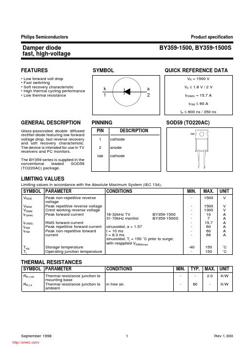
Philips Semiconductors Product specificationDamper diode BY359-1500, BY359-1500Sfast, high-voltageFEATURESSYMBOL QUICK REFERENCE DATA• Low forward volt drop • Fast switching• Soft recovery characteristic• High thermal cycling performance • Low thermal resistanceGENERAL DESCRIPTIONPINNINGSOD59 (TO220AC)Glass-passivated double diffused PIN DESCRIPTION rectifier diode featuring low forward voltage drop,fast reverse recovery 1cathode and soft recovery characteristic.The device is intended for use in TV 2anode receivers and PC monitors.tabcathodeThe BY359series is supplied in the conventional leaded SOD59(TO220AC)package.LIMITING VALUESLimiting values in accordance with the Absolute Maximum System (IEC 134).SYMBOL PARAMETERCONDITIONSMIN.MAX.UNIT V RSM Peak non-repetitive reverse -1500V voltageV RRM Peak repetitive reverse voltage -1500V V RWM Crest working reverse voltage -1300V I F(peak)Peak forward current16-32kHz TVBY359-1500 -10A 31-70kHz monitor BY359-1500S-7A I F(RMS)RMS forward current-15.7A I FRM Peak repetitive forward current sinusoidal; a = 1.57-60A I FSMPeak non-repetitive forward t = 10 ms -60A currentt = 8.3 ms-66A sinusoidal; T j = 150 ˚C prior to surge;with reapplied V RWM(max)T stg Storage temperature-40150˚C T jOperating junction temperature-150˚CTHERMAL RESISTANCESSYMBOL PARAMETERCONDITIONSMIN.TYP.MAX.UNIT R th j-mb Thermal resistance junction to -- 2.0K/W mounting baseR th j-aThermal resistance junction to in free air.-60-K/Wambient1tab2Philips Semiconductors Product specificationDamper diode BY359-1500, BY359-1500Sfast, high-voltageSTATIC CHARACTERISTICST j = 25 ˚C unless otherwise statedBY359-1500BY359-1500S SYMBOL PARAMETER CONDITIONS TYP.MAX.TYP.MAX.UNIT V F Forward voltage I F = 20 A1.3 1.8 1.52.0V I F = 10 A; T j = 150˚C 1.00 1.5 1.25 1.75V I RReverse currentV R = 1300 V 1010010100µA V R = 1300 V;50300100600µAT j = 100 ˚CDYNAMIC CHARACTERISTICST j = 25 ˚C unless otherwise statedBY359-1500BY359-1500S SYMBOL PARAMETERCONDITIONS TYP.MAX.TYP.MAX.UNIT t rr Reverse recovery time I F = 2 A; V R ≥ 30 V;0.470.600.280.35µs Q s Reverse recovery charge -dI F /dt = 20 A/µs 1.6 2.00.700.95µC V frPeak forward recovery voltageI F = 10 A;11.0-17.0-VdI F /dt = 30 A/µsPhilips Semiconductors Product specificationDamper diode BY359-1500, BY359-1500Sfast, high-voltagePhilips Semiconductors Product specificationDamper diode BY359-1500, BY359-1500Sfast, high-voltageMECHANICAL DATANotes1. Refer to mounting instructions for TO220 envelopes.2. Epoxy meets UL94 V0 at 1/8".Philips Semiconductors Product specification Damper diode BY359-1500, BY359-1500S fast, high-voltageDEFINITIONSData sheet statusObjective specification This data sheet contains target or goal specifications for product development. Preliminary specification This data sheet contains preliminary data; supplementary data may be published later. Product specification This data sheet contains final product specifications.Limiting valuesLimiting values are given in accordance with the Absolute Maximum Rating System (IEC 134). Stress above one or more of the limiting values may cause permanent damage to the device. These are stress ratings only and operation of the device at these or at any other conditions above those given in the Characteristics sections ofthis specification is not implied. Exposure to limiting values for extended periods may affect device reliability. Application informationWhere application information is given, it is advisory and does not form part of the specification.© Philips Electronics N.V. 1998All rights are reserved. Reproduction in whole or in part is prohibited without the prior written consent of the copyright owner.The information presented in this document does not form part of any quotation or contract, it is believed to be accurate and reliable and may be changed without notice. No liability will be accepted by the publisher for any consequence of its use. Publication thereof does not convey nor imply any license under patent or other industrial or intellectual property rights.LIFE SUPPORT APPLICATIONSThese products are not designed for use in life support appliances, devices or systems where malfunction of these products can be reasonably expected to result in personal injury. Philips customers using or selling these products for use in such applications do so at their own risk and agree to fully indemnify Philips for any damages resulting from such improper use or sale.分销商库存信息: NXPBY359-1500,127。
8896;8897;8898;8899;中文规格书,Datasheet资料

pending design and can be used for the following applications:MSD (Moisture Sensitive Device)re-baking process The current method of identification of unpacked moisture sensitive devices (MSDs)during the re-baking process,is typically done manually by pasting papers on IC trays with written information such as date and time of unpacking.Since this information is important for maintaining MSDs performance,once manually noted baking trays are put into an oven for re-baking,it is hard to identify individual trays to determine which one should be removed first.With the Anti-Static Clip,this process is made easy,thanks to unique color coding.Identification for IC production lineThere are several ways to identify ICs at the manufacturing level.For example,drawing a line on an IC tray with a marker is common.However,with this done an IC tray with a drawn line cannot be re-used for other purposes.Now with the color coded Anti-Static IC Tray Clip,operators can sort and reuse IC trays for various purposes with ease.CAT.NO.COLOR8894WHITE 8895BLUE 8896YELLOW 8897ORANGE 8898PINK 8899GREENCAT.NO.L A B 8620 2.5(63.5) 2.0(50.8)—8621 3.0(76.2) 2.5(63.5)—8622 3.5(88.9) 3.0(76.2)—8623 4.0(101.6) 3.5(88.9)—8624 4.5(114.3) 4.0(101.6)—8625 5.0(127.0) 4.5(114.3)—8626 5.5(139.7) 5.0(127.0)—8627 6.0(152.4) 5.5(139.7)—8628 6.5(165.1) 6.0(152.4)—86297.0(177.8) 6.5(165.1)—86307.0(177.8) 6.5(165.1) 3.25(82.6)86317.5(190.5)7.0(177.8)—86327.5(190.5)7.0(177.8) 3.50(88.9)86338.0(203.2)7.5(190.5)—86348.0(203.2)7.5(190.5) 3.75(95.3)86358.5(215.9)8.0(203.2)—86368.5(215.9)8.0(203.2)4.00(101.6)•Designed for .062(1.57)PC cards.•Level action ejectors aids cardinsertion and extraction.•Supplied complete with stainless steel spring pin.LEVER ACTION PC CARD EJECTORSCARD MOUNTING DIMENSIONSPC BOARD GUIDES.109[2.8]DIA.MOUNTING HOLE.250[6.4].250 [6.4]PC CARD.250 [6.4].140 [3.6]RADIUS.093[2.36]DIA.1.125 [28.6].450 [11.5].640 [16.3].075 [1.90].250[6.4].375[9.6]CAT.NO.8640CAT.NO.8644CAT.NO.8643CAT.NO.8641CAT.NO.8642.075 [1.90].390[9.9].640 [16.3].450 [11.5]1.125 [28.6].093[2.36]DIA..140 [3.6]RADIUS.250 [6.4].375[9.5] 1.100 [28.0].140[3.6]RADIUS.390[9.9].075 [1.90].250[6.4].093[2.36]DIA..520[13.2].600[15.3].093[2.36]DIA..140 [3.6]RADIUS1.250 [31.8].075 [1.90].250 [6.4].290[7.4].134[3.4].260 [6.6].250[6.4].140 [3.6]RADIUS.093[2.36]DIA..980 [24.9].375[9.5].640[16.3].390[9.9].125[3.2].075[1.90]Guides may be used horizontally or vertically and snap into .125(3.2)diameter holes.Narrow width allows maximum density and optimum airflow.Simple press-fit,secure installation.MATERIAL:Natural Nylon 6/6,UL Rated 94V-2B.125[3.2].250[6.4].132 [3.4].078 [2.0].245[6.2]LA.085[2.2].172[4.4]REF ..185[4.7].197[5.01].205[5.2].984[25.0].394[10.0].075[1.90]Mounting Detail.218 [5.6](2)PLS.120[3.1](2)PLSAB.125 [3.2] DIA .SPECIFICATIONSMaterial:Nylon 6/6,UL Rated 94V-0Surface Resistance:≤1x 10¹²ΩOperating Temperature:300°F (150°C)Max.MATERIAL:White Nylon 6/6,UL Rated 94V-2Tel (718)956-8900•Fax (718)956-9040(800)221-5510•kec@31-0720th Road –Astoria,NY 11105-2017RoHS COMPLIANT ~ISO 9001CERTIFIED®Patent Pending•The Anti-Static IC tray clip is designed to perfectly fit into a JEDEC tray.It is flexible and may be clipped securely into IC tray tab.P C B O A R D A C C E S S O R I E S122分销商库存信息:KEYSTONE-ELECTRONICS889688978898 8899。
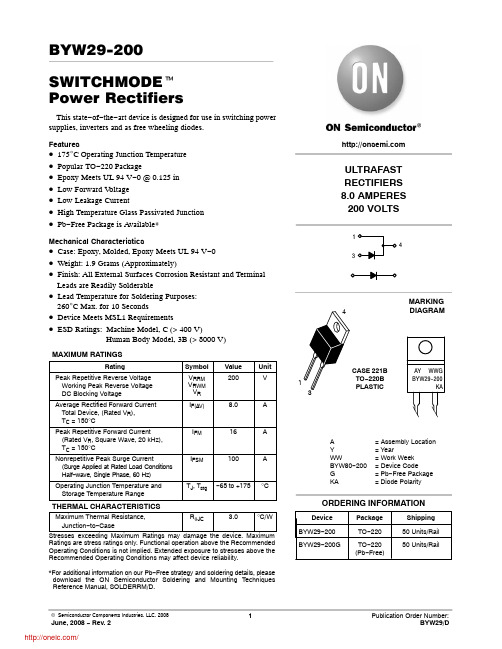
BYW29-200G;中文规格书,Datasheet资料
0.5 1.0 2.0
5.0 10
20
t, TIME (ms)
Figure 6. Thermal Response
50 100 200
ULTRAFAST RECTIFIERS 8.0 AMPERES 200 VOLTS
1 4
3
MARKING
4
DIAGRAM
1 3
CASE 221B TO−220B PLASTIC
AY WWG BYW29-200
KA
A Y WW BYW80−200 G KA
= Assembly Location = Year = Work Week = Device Code = Pb−Free Package = Diode Polarity
2
IF(AV), AVERAGE FORWARD CURRENT (AMPS)
r(t), TRANSIENT THERMAL RESISTANCE (NORMALIZED)
BYW29−200
PF(AV), AVERAGE POWER DISSIPATION (WATTS)
*For additional information on our Pb−Free strategy and soldering details, please download the ON Semiconductor Soldering and Mounting Techniques Reference Manual, SOLDERRM/D.
SF2027B;中文规格书,Datasheet资料

Electrical CharacteristicsCharacteristicSym Notes MinTyp MaxUnits Nominal Frequency f N1199.0MHz Insertion Loss(including matching to 200 ohms)IL< 7.0dB Group Delay Ripple, peak - peak (198.9 .. 199.1 MHz)< 700ns Amplitude Ripple, peak - peak (198.9 .. 199.1 MHz)< 1.0dBRelative attenuation fn - 100 kHz .. fn +100 kHz (passband)< 0.7fn - 300 kHz, fn +300 kHz > 10dB fn - 500 kHz, fn +500 kHz > 27dB fn - 600 kHz, fn +600 kHz > 36dB <fn - 700 kHz,> fn +700 kHz> 45dBCase StyleSMP-53-S 13.3 X 6.5 mm Nominal FootprintLid Symbolization (Y=year, WW=week, S=shift) See note 4RFM SF2027B YWWS•GSM BTS Receiver IF Applications •Small Size•Hermetic 13.3 X 6.5 mm Surface Mount CaseInput power Level short test+18 dBm standard operation, max +10 dBm Max DC Voltage between any 2 terminals10VInput: possible for balanced and unbalanced operation (TBD)Output: BalancedExternal matching to 50 or 200 ohms199.0 MHz SAW FilterSF2027B 1.Unless noted otherwise, all specifications apply over the operating temperaturerange with filter soldered to the specified demonstration board with impedancematching to 50 Ω and measured with 50 Ω network analyzer. A dB offset existsfor RFM because of the loss introduced by using transformers on the Input and Output.2.Rejection is measured as attenuation below the minimum IL point in the pass-band. Rejection in final user application is dependent on PCB layout and exter-nal impedance matching design. See Application Note No. 42 for details.3."LRIP" or "L" after the part number indicates "low rate initial production" and"ENG" or "E" indicates "engineering prototypes."4.The design, manufacturing process, and specifications of this filter are subject to change.5.Either Port 1 or Port 2 may be used for either input or output in the design. However, impedances and impedance matching may vary between Port 1 and Port 2, so that the filter must always be installed in one direction per the circuit design. and international patents may apply.7.RFM, stylized RFM logo, and RF Monolithics, Inc. are registered trademarks of RF Monolithics, Inc.8.©Copyright 1999, RF Monolithics Inc.9.Electrostatic Sensitive Device. Observe precautions for handling.Notes:Carrier Tape DimensionsAo .274 ± .004 (7.0)Bo .542 ± .004 (13.76)Ko .088 ± .004 (2.2)P 12mm W 24mm Tape Length 86M Pockets/M83/M“B “Nominal Size Quantity Per ReelInches millimeters7178500133301000Tape and Reel SpecificationsCOMPONENT ORIENTATION and DIMENSIONSUSER DIRECTION OF FEEDPIN #1SMP-53-S CaseDimensionmm Inches MinNom MaxMinNom MaxA 13.3.524B 6.5.256C 2.00.078D 2.3.091E 1.91.075F 1.02.040G1.00.039ConnectionTerminalsPort 1 Input Hot1Port 1 Input Gnd Return 10Port 2 Output Hot6Port 2 Output Gnd Return 5Case GroundAll others Single Ended Operation Return is ground Differential OperationReturn is hot10-Terminal Ceramic Surface-Mount Case13.3 x 6.5 mm Nominal FootprintElectrical ConnectionsCase DimensionsSolder Temperature ProfileFigure 1 shows the recommended temperature profile for reflow soldering SMP-03 and SMP53-S package consists of a ceramic base with a metal lid that is attached with high-temperature solde age is hermetically sealed and the solder seal must not be compromised with excessive heat in a ical that the filter package is never heated above 250°C. It is recommended that the package b than 240°C for no more than 10 seconds.分销商库存信息: RFMSF2027B。
CM1623-04DE;中文规格书,Datasheet资料

CM1623EMI Filter with ESDProtection for SIM Card ApplicationsFeatures•4−Channel EMI Filtering with Integrated ESD Protection•Pi −Style EMI Filters in a Capacitor −Resistor −Capacitor (C −R −C)Network•±15 kV ESD Protection on Each Channel (IEC 61000−4−2 Level 4, Contact Discharge)•8−Lead UDFN Package with 0.40 mm Pitch•Tiny UDFN Package Size: 1.7 mm x 1.35 mm x 0.5 mm •Increased Robustness Against Vertical Impacts During Manufacturing Process•These Devices are Pb −Free and are RoHS CompliantELECTRICAL SCHEMATIC*See Package/Pinout Diagrams for expanded pin information.MARKING DIAGRAMDevice Package Shipping †ORDERING INFORMATIONCM1623−04DEUDFN −8(Pb −Free)3000/T ape & ReelUDFN8DE SUFFIX CASE 517BC†For information on tape and reel specifications,including part orientation and tape sizes, please refer to our Tape and Reel Packaging Specification Brochure, BRD8011/D.P23 M G G1P23= CM1623−04DE M = Date Code G = Pb −Free Package(Note: Microdot may be in either location)Table 1. PIN DESCRIPTIONS8−Lead UDFN PackagePin Name Description1RST Filter + ESD Channel 1 2CLK Filter + ESD Channel 2 3DATA Filter + ESD Channel 3 4VCC V ExternalGNDPAD GND Device Ground8RST Filter + ESD Channel 1 7CLK Filter + ESD Channel 2 6DATA Filter + ESD Channel 3 5VCC V ExternalPACKAGE / PINOUT DIAGRAMSCM1623−04DE8−Lead UDFN PackageTop View(Pins Down View)Bottom View(Pins Up View)12348765GNDPAD SPECIFICATIONSTable 2. ABSOLUTE MAXIMUM RATINGSParameter Rating Units Storage Temperature Range−65 to +150°C DC Power per Resistor100mW DC Package Power Rating500mW Stresses exceeding Maximum Ratings may damage the device. Maximum Ratings are stress ratings only. Functional operation above the Recommended Operating Conditions is not implied. Extended exposure to stresses above the Recommended Operating Conditions may affect device reliability.Table 3. STANDARD OPERATING CONDITIONSParameter Rating Units Operating Temperature Range−40 to +85°C Table 4. ELECTRICAL OPERATING CHARACTERISTICS (Note 1)Symbol Parameter Conditions Min Typ Max Units R1Reset Channel Resistance80100120W R2Clock Channel Resistance37.64756.4W R3Data Channel Resistance80100120W C1Capacitance on Pins 1, 2, and 3At 1 MHz, V IN = 0 V162024pF C2Capacitance on Pins 4 and 5At 1 MHz, V IN = 0 V18pFI LEAK Diode Leakage Current (Reverse Bias)V DIODE= 3.3 V0.1 1.0m AV SIG Signal Clamp Voltagea) Positive Clampb) Negative Clamp I LOAD = 10 mAI LOAD = −10 mA5.6−1.56.8−0.89.0−0.4VV ESD ESD Peak Discharge Voltage Protection on All Pins In−system ESD Withstand Voltage:a) Contact Discharge per IEC 61000−4−2 Level 4b) Air Discharge per IEC 61000−4−2 Level 4T A = 25°C(Note 2)±15±15±15±15kV1.All parameters specified at T A= 25°C unless otherwise noted.2.Standard IEC 61000−4−2 with C Discharge = 150 pF, R Discharge = 330 W.PERFORMANCE INFORMATIONTypical Filter Performance (T A = 255C, DC Bias = 0 V, 50 W Environment)Figure 1. Insertion Loss vs. Frequency, Filter 1 (Pins 1 and 8)Figure 2. Insertion Loss vs. Frequency, Filter 2 (Pins 2 and 7)Typical Filter Performance (T A = 255C, DC Bias = 0 V, 50 W Environment)Figure 3. Insertion Loss vs. Frequency, Filter 3 (Pins 3 and 6)Figure 4. Insertion Loss vs. Frequency, Filter 4 (Pins 4 and 5)Figure 5. Diode Capacitance vs. Input Voltage (Normalized to Capacitance at 0 VDC and 255C)PACKAGE DIMENSIONSUDFN8, 1.7x1.35, 0.4P CASE 517BC −01ISSUE ONOTES:1.DIMENSIONING AND TOLERANCING PER ASME Y14.5M, 1994.2.CONTROLLING DIMENSION: MILLIMETERS.3.DIMENSION b APPLIES TO PLATED TERMINAL AND IS MEASURED BETWEEN 0.15 AND 0.25 mm FROM THE TERMINAL TIP .4.COPLANARITY APPLIES TO THE EXPOSED PAD AS WELL AS THE TERMINALS.BOTTOM VIEWL8XDIM MIN MAX MILLIMETERS A 0.450.55A10.000.05A30.13 REF b 0.150.25D 1.70 BSC D2 1.10 1.30E 1.35 BSC E20.300.50e 0.40 BSC K 0.15−−−L 0.200.300.50DIMENSIONS: MILLIMETERS*For additional information on our Pb −Free strategy and soldering details, please download the ON Semiconductor Soldering and Mounting Techniques Reference Manual, SOLDERRM/D.SOLDERING FOOTPRINT*L1−−−0.05DETAIL BALTERNATE CONSTRUCTIONSL1DETAIL ALALTERNATE TERMINAL CONSTRUCTIONSRECOMMENDEDON Semiconductor and are registered trademarks of Semiconductor Components Industries, LLC (SCILLC). SCILLC reserves the right to make changes without further notice to any products herein. SCILLC makes no warranty, representation or guarantee regarding the suitability of its products for any particular purpose, nor does SCILLC assume any liability arising out of the application or use of any product or circuit, and specifically disclaims any and all liability, including without limitation special, consequential or incidental damages.“Typical” parameters which may be provided in SCILLC data sheets and/or specifications can and do vary in different applications and actual performance may vary over time. All operating parameters, including “Typicals” must be validated for each customer application by customer’s technical experts. SCILLC does not convey any license under its patent rights nor the rights of others. SCILLC products are not designed, intended, or authorized for use as components in systems intended for surgical implant into the body, or other applications intended to support or sustain life, or for any other application in which the failure of the SCILLC product could create a situation where personal injury or death may occur. Should Buyer purchase or use SCILLC products for any such unintended or unauthorized application, Buyer shall indemnify and hold SCILLC and its officers, employees, subsidiaries, affiliates,and distributors harmless against all claims, costs, damages, and expenses, and reasonable attorney fees arising out of, directly or indirectly, any claim of personal injury or death associated with such unintended or unauthorized use, even if such claim alleges that SCILLC was negligent regarding the design or manufacture of the part. SCILLC is an Equal Opportunity/Affirmative Action Employer. This literature is subject to all applicable copyright laws and is not for resale in any manner.PUBLICATION ORDERING INFORMATION分销商库存信息: ONSEMICM1623-04DE。
PVD2352N;中文规格书,Datasheet资料

Data Sheet No. PD10053 revISeries PVD33N & PbFMicroelectronic Power ICHEXFET ® Power MOSFET Photovoltaic RelaySingle-Pole, Normally-Open0-300V DC, 240mAGeneral DescriptionThe PVD33 Series DC Relay (PVD) is a single-pole,normally open, solid-state replacement for electromechanical relays used for general purpose switching of analog signals. It utilizes International Rectifier’s HEXFET power MOSFET as the output switch, driven by an integrated circuit photovoltaic generator of novel construction. The output switch is controlled by radiation from a GaAlAs light emitting diode (LED), which is optically isolated from the photovoltaic generator.The PVD33 Series overcomes the limitations of both conventional electromechanical and reed relays by offering the solid state advantages of long life, fast operating speed, low pick up power, bounce-free operation, low thermal offset voltages and miniature package. These advantages allow product improvement and design innovations in many applications such as process control, multiplexing,automatic test equipment and data acquisition.The PVD33 can switch analog signals from thermocouple level to 300 Volts peak DC. Signal frequencies into the RF range are easily controlled and switching rates up to 500Hz are achievable. The extremely small thermally generated offset voltages allow increased measurement accuracies.These relays are packaged in 8-pin, molded DIP packages and available with either thru-hole or surface-mount (“gull-wing”) leads, in plastic shipping tubes.Applications§Process Control §Data Acquisition §Test Equipment§Multiplexing and ScanningFeatures§ Bounce-Free Operation §1010 Off-State Resistance §1,000 V/µsec dv/dt § 5 mA Input Sensitivity §4,000 V RMS I/O Isolation §Solid-State Reliability §UL Recognized §ESD Tolerance:4000V Human Body Model 500V Machine Model(HEXFET is the registered trademark for International Rectifier Power MOSFETs)Part IdentificationPVD2352N & PbF PVD3354N & PbFPVD2352NS & PbF PVD3354NS & PbFsurface-mount (gull-wing) 1thru-holeOBSOLETESeries PVD33N & PbF 2Electrical Specifications (-40°C ≤ T A ≤ +85°C unless otherwise specified )International Rectifier does not recommend the use of this product in aerospace, avionics, military or life support ers of this International Rectifier product in such applications assume all risks of such use and indemnify International Rectifier against all damages resulting from such use.Series PVD33N & PbF3Figure 1. Current Derating CurvesFigure 2. Typical Control Current RequirementsFigure 4. Typical On-ResistanceR D (o n ) (N o r m a l i z e d25o C )I LED (mA)M a x . L o a d C u r r e n t (m A )Ambient Temperature (°C)5 mA Control l D = 50 mASeries PVD33N & PbF 4I D O f f /I D O f f 25°CFigure 5. Normalized Off-State LeakageFigure 6. Input Characteristics(Current Controlled)Figure 7.Typical Delay TimesFigure 8. Delay Time DefinitionsLED Forward Voltage Drop (Volts DC)I n p u t C u r r e n t (m A )Ambient Temperature (°C)Series PVD33N & PbFWiring DiagramIR WORLD HEADQUARTERS: 233 Kansas St., El Segundo, California 90245 Tel: (310) 252-7105Data and specifications subject to change without notice. 2/2008 6分销商库存信息: IRPVD2352N。
WP914CK4GDT;中文规格书,Datasheet资料

/
SPEC NO: DSAF3501 APPROVED: WYNEC
REV NO: V.5 CHECKED: Allen Liu
DATE: APR/09/2011 DRAWN: J.Yu
PAGE
PACKING & LABEL SPECIFICATIONS
WP914CK/4GDT
SPEC NO: DSAF3501 APPROVED: WYNEC
REV NO: V.5 CHECKED: Allen Liu
DATE: APR/09/2011 DRAWN: J.Yu
PAGE: 4 OF 5 ERP: 1102002264
分销商库存信息:
KINGBRIGHT WP914CK/4GDT
2x3mm QUAD-LEVEL LED INDICATOR
Part Number: WP914CK/4GDT Green
Features
z Quad-level design, save board space. z Different color combination available . z Black case enhances contrast. z Housing UL rating:94V-0. z Housing material: type 66 nylon. z RoHS compliant.
SPEC NO: DSAF3501 APPROVED: WYNEC
REV NO: V.5 CHECKED: Allen Liu
DATE: APR/09/2011 DRAWN: J.Yu
PAGE: 1 OF 5 ERP: 1102002264
/
Selection Guide
IRF7755;中文规格书,Datasheet资料
PD -93995AIRF7755HEXFET® Power MOSFETl l l l lUltra Low On-Resistance Dual P-Channel MOSFET Very Small SOIC Package Low Profile (< 1.2mm) Available in Tape & ReelVDSS-20VRDS(on) max51mΩ@VGS = -4.5V 86mΩ@VGS = -2.5VID-3.7A -2.8ADescriptionHEXFET® Power MOSFETs from International Rectifier utilize advanced processing techniques to achieve extremely low on-resistance per silicon area. This benefit, combined with the ruggedized device design, that International Rectifier is well known for, provides thedesigner1 2 3 4 1= 2= 3= 4= D1 S1 S1 G1 8= 7= 6= 5= 8 7 6 5 D2 S2 S2 G2with an extremely efficient and reliable device for battery and load management.The TSSOP-8 package has 45% less footprint area than the standard SO-8. This makes the TSSOP-8 an ideal device for applications where printed circuit board space is at a premium. The low profile (<1.2mm) allows it to fit easily into extremely thin environments such as portable electronics and PCMCIA cards.TSSOP-8Absolute Maximum RatingsParameterVDS ID @ TA = 25°C ID @ TA = 70°C IDM PD @TA = 25°C PD @TA = 70°C VGS TJ , TSTG Drain-Source Voltage Continuous Drain Current, VGS @ -4.5V Continuous Drain Current, VGS @ -4.5V Pulsed Drain Current Maximum Power Dissipation Maximum Power Dissipation Linear Derating Factor Gate-to-Source Voltage Junction and Storage Temperature RangeMax.-20 -3.9 -3.1 -15 1 0.64 0.01 ±20 -55 to +150UnitsV A W W W/°C V °CThermal ResistanceParameterRθJA Maximum Junction-to-AmbientMax.125Units°C/W14/9/01/IRF7755Electrical Characteristics @ TJ = 25°C (unless otherwise specified)V(BR)DSS∆V(BR)DSS/∆TJParameter Drain-to-Source Breakdown Voltage Breakdown Voltage Temp. Coefficient Static Drain-to-Source On-Resistance Gate Threshold Voltage Forward Transconductance Drain-to-Source Leakage Current Gate-to-Source Forward Leakage Gate-to-Source Reverse Leakage Total Gate Charge Gate-to-Source Charge Gate-to-Drain ("Miller") Charge Turn-On Delay Time Rise Time Turn-Off Delay Time Fall Time Input Capacitance Output Capacitance Reverse Transfer CapacitanceRDS(on) VGS(th) gfs IDSS IGSS Qg Qgs Qgd td(on) tr td(off) tf Ciss Coss CrssMin. -20 ––– ––– ––– -0.45 7.0 ––– ––– ––– ––– ––– ––– ––– ––– ––– ––– ––– ––– ––– –––Typ. ––– 0.011 35.3 44.3 ––– ––– ––– ––– ––– ––– 11 2.1 3.5 9 13 89 61 1090 182 124Max. Units Conditions ––– V VGS = 0V, ID = -250µA ––– V/°C Reference to 25°C, ID = -1mA 51 VGS = -4.5V, ID = -3.7A mΩ 86 VGS = -2.5V, ID = -2.8A -1.2 V VDS = VGS, ID = -250µA ––– S VDS = -10V, ID = -3.7A -15 VDS = -16V, VGS = 0V µA -25 VDS = -16V, VGS = 0V, TJ = 70°C -100 VGS = -12V nA 100 VGS = 12V 17 ID = -3.7A ––– nC VDS = -16V ––– VGS = -4.5V 14 VDD = -10V, VGS = -4.5V 20 ID = -1.0A ns 133 RG = 6.0Ω 92 RD = 10Ω ––– VGS = 0V ––– pF VDS = -15V ––– ƒ = 1.0MHzSource-Drain Ratings and CharacteristicsISISMVSD trr QrrParameter Continuous Source Current (Body Diode) Pulsed Source Current (Body Diode) Diode Forward Voltage Reverse Recovery Time Reverse Recovery ChargeMin. Typ. Max. Units ––– ––– ––– ––– ––– ––– ––– ––– 55 29 -1.0 A -15 -1.2 82 43 V ns nCConditions MOSFET symbol showing the G integral reverse p-n junction diode. TJ = 25°C, IS = -1.0A, VGS = 0V TJ = 25°C, I F = -1.0A di/dt = -100A/µs DSNotes: Repetitive rating; pulse width limited bymax. junction temperature. When mounted on 1 inch square copper board, t < 10sec. Pulse width ≤ 300µs; duty cycle ≤ 2%.2/IRF7755100VGS -7.5V -4.5V -3.5V -3.0V -2.5V -2.0V -1.75V BOTTOM -1.5V TOP100VGS -7.5V -4.5V -3.5V -3.0V -2.5V -2.0V -1.75V BOTTOM -1.5V TOP-ID, Drain-to-Source Current (A)10-ID, Drain-to-Source Current (A)1011-1.5V-1.5V 20µs PULSE WIDTH Tj = 25°C0.1 0.1 1 10 10020µs PULSE WIDTH Tj = 150°C0.1 0.1 1 10 100-VDS, Drain-to-Source Voltage (V)-VDS, Drain-to-Source Voltage (V)Fig 1. Typical Output CharacteristicsFig 2. Typical Output Characteristics1002.0RDS(on) , Drain-to-Source On Resistance (Normalized)ID = -3.9A-I D , Drain-to-Source Current (A)1.510TJ = 150 ° C TJ = 25 ° C11.00.50.1 1.0V DS = -15V 20µs PULSE WIDTH 1.5 2.0 2.5 3.00.0 -60 -40 -20VGS = -4.5V0 20 40 60 80 100 120 140 160-VGS , Gate-to-Source Voltage (V)TJ , Junction Temperature ( ° C)Fig 3. Typical Transfer CharacteristicsFig 4. Normalized On-Resistance Vs. Temperature3/IRF77551600-VGS , Gate-to-Source Voltage (V)VGS = 0V, f = 1MHz Ciss = Cgs + Cgd , Cds SHORTED Crss = Cgd Coss = Cds + Cgd10ID = -3.7AV DS =-16V8C, Capacitance (pF)1200Ciss68004400Coss Crss0 1 10 10020 0 4 8 12 16 20-VDS , Drain-to-Source Voltage (V)QG , Total Gate Charge (nC)Fig 5. Typical Capacitance Vs. Drain-to-Source VoltageFig 6. Typical Gate Charge Vs. Gate-to-Source Voltage100100-ISD , Reverse Drain Current (A)OPERATION IN THIS AREA LIMITED BY RDS(on)10-I ID , Drain Current (A)10100usTJ = 150 ° C TJ = 25 ° C1ms1110ms0.1 0.2V GS = 0 V0.4 0.6 0.8 1.0 1.2 1.40.1 0.1TC = 25 °C TJ = 150 °C Single Pulse1 10 100-VSD ,Source-to-Drain Voltage (V)-VDS , Drain-to-Source Voltage (V)Fig 7. Typical Source-Drain Diode Forward VoltageFig 8. Maximum Safe Operating Area4/IRF77554.0VDS VGSRD-ID , Drain Current (A)3.0D.U.T.+RGVDD2.0VGSPulse Width ≤ 1 µs Duty Factor ≤ 0.1 %Fig 10a. Switching Time Test Circuit1.0td(on) tr t d(off) tfVGS0.0 25 50 75 100 125 15010%TC , Case Temperature ( ° C)Fig 9. Maximum Drain Current Vs. Case Temperature90% VDSFig 10b. Switching Time Waveforms1000Thermal Response (Z thJA )100D = 0.50 0.20 0.10100.05 0.02 0.01 PDM t1 t2 SINGLE PULSE (THERMAL RESPONSE) Notes: 1. Duty factor D = t 1 / t 2 2. Peak TJ = P DM x ZthJA + TA 0.01 0.1 1 10 10010.1 0.000010.00010.001t1 , Rectangular Pulse Duration (sec)Fig 11. Maximum Effective Transient Thermal Impedance, Junction-to-Ambient5/IRF7755Ω) RDS ( on ) , Drain-to-Source On Resistance (() RDS(on), Drain-to -Source On Resistance Ω0.1600.2000.1200.1500.0800.100VGS = -2.5VID = -3.7A0.0400.050VGS = -4.5V0.000 2.0 3.0 4.0 5.0 6.0 7.0 8.00.000 0 5 10 15 -ID , Drain Current ( A )-VGS, Gate -to -Source Voltage (V)Fig 12. Typical On-Resistance Vs. Gate VoltageFig 13. Typical On-Resistance Vs. Drain CurrentCurrent Regulator Same Type as D.U.T.50KΩQG12V.2µF.3µF10 VQGS VG QGDVGS-3mAD.U.T.+VDSIGIDCurrent Sampling ResistorsChargeFig 14a. Basic Gate Charge WaveformFig 14b. Gate Charge Test Circuit6/IRF7755TSSOP-8 Part Marking InformationEXAMPLE: T HIS IS AN IRF7702LOT CODE (XX) PART NUMBERDAT E CODE (YW)XXYW 7702T ABLE 1 WORK WEEK 1-26, NUMERIC YEAR CODE (1,2, ....ET C.) YEAR 2001 2002 2003 1994 1995 1996 1997 1998 1999 2000 Y 1 2 3 4 5 6 7 8 9 0 WORK WEEK 01 02 03 04 W A B C DDAT E CODE EXAMPLES : 9503 = 5C 9532 = EF24 25 26X Y ZT ABLE 2 WORK WEEK 27-52, ALPHANUMERIC YEAR CODE (A,B, ...ETC.) YEAR 2001 2002 2003 1994 1995 1996 1997 1998 1999 2000 Y A B C D E F G H J K WORK WEEK 27 28 29 30 W A B C D50 51 52X Y ZTSSOP-8 Tape and Reel8LT SSOP (MO-153AA)16 mmØ 13"16mm 8 mm FEED DIRECT ION NOT ES: 1. T APE & REEL OUT LINE CONFORMS T O EIA-481 & EIA-541.7/IRF7755TSSOP-8 Package OutlineData and specifications subject to change without notice. This product has been designed and qualified for the consumer market. Qualification Standards can be found on IR’s Web site.IR WORLD HEADQUARTERS: 233 Kansas St., El Segundo, California 90245, USA Tel: (310) 252-7105 TAC Fax: (310) 252-7903 Visit us at for sales contact information. 4/018/分销商库存信息:IR IRF7755。
60499;中文规格书,Datasheet资料

In addition, our products have these details: • • • • • • • • • • Machined stainless steel studs on wrist straps Patented contoured banana plugs Custom molded coil cords Soft-fold bag construction Hip-to-cuff grounded smocks Matting with lifetime electricals Non-humidity dependent mats and bags Low charging dissipative floor finish Dual-wire and single-wire continuous monitors Ionizers with removable emitter cassette - superior feedback controls
Table of Contents These details separate Desco from all the rest:
• • • • • • • • • We make most what we sell We manufacture in the USA Product support personnel Online technical bulletins and drawings Patented and trademarked products We sell through regional, national and international distribution ESD surveys and training Superior warranties Satisfaction guaranteed
74435561100;中文规格书,Datasheet资料

74435561100
DATUM / DATE : 2009-11-02 Gurtspezifikation / Tape specification:
G H
SPEICHERDROSSEL WE-HCI POWER-CHOKE WE-HCI
I Rollenspezifikation / tape and reel specification:
74435561100
DATUM / DATE : 2009-11-02
SPEICHERDROSSEL WE-HCI POWER-CHOKE WE-HCI
H Induktivitätskurve / Inductance curve:
Induktivität vs Strom (typ.) Inductance vs Current (typ.)
08-09-29
Geprüft / checked
Kontrolliert / approved
Datum / date
D-74638 Waldenburg · Max-Eyth-Strasse 1 - 3 · Germany · Telefon (+49) (0) 7942 - 945 - 0 · Telefax (+49) (0) 7942 - 945 - 400 http://www.we-online.de
12,00
10,00
8,00
L (µH)
6,00
4,00
2,00
0,00 0 5 10 15 Current (A) 20 25 30 35
Freigabe erteilt / general release:
..................................................................................
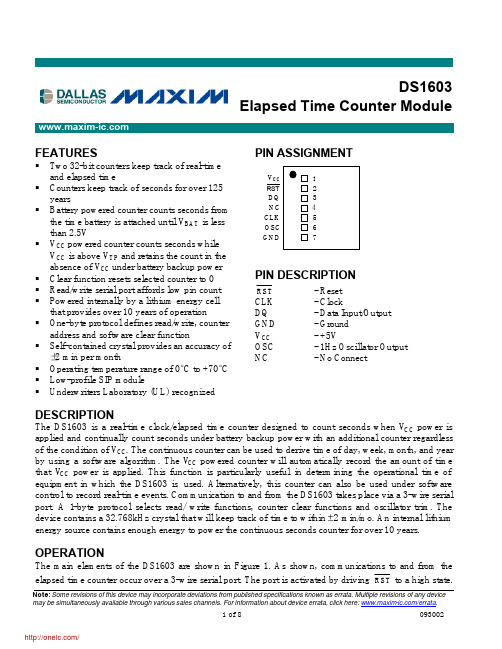
DS1603;中文规格书,Datasheet资料
Note: Some revisions of this device may incorporate deviations from published specifications known as errata. Multiple revisions of any device may be simultaneously available through various sales channels. For information about device errata, click here: /errata .FEATURES§ Two 32-bit counters keep track of real -time and elapsed time§ Counters keep track of seconds for over 125 years§ Battery powered counter counts seconds from the time battery is attached until V BAT is less than 2.5V§ V CC powered counter counts seconds while V CC is above V TP and retains the count in the absence of V CC under battery backup power § Clear function resets selected counter to 0 § Read/write serial port affords low pin count § Powered internally by a lithium energy cell that provides over 10 years of operation§ One-byte protocol defines read/write, counter address and software clear function§ Self-contained crystal provides an accuracy of ±2 min per month§ Operating temperature range of 0°C to +70°C § Low-profile SIP module§ Underwriters Laboratory (UL) recognized PIN ASSIGNMENTPIN DESCRIPTIONRST- Reset CLK - ClockDQ - Data Input/Output GND - Ground V CC - +5VOSC - 1Hz Oscillator Output NC- No ConnectDESCRIPTIONThe DS1603 is a real -time clock/elapsed time counter designed to count seconds when V CC power is applied and continually count seconds under battery backup power with an additional counter regardless of the condition of V CC . The continuous counter can be used to derive time of day, week, month, and year by using a software algorithm. The V CC powered counter will automatically record the amount of time that V CC power is applied. This function is particularly useful in determining the operational time of equipment in which the DS1603 is used. Alternatively, this counter can also be used under software control to record real -time events. Communication to and from the DS1603 takes place via a 3-wire serial port. A 1-byte protocol selects read/ write functions, counter clear functions and oscillator trim. The device contains a 32.768kHz crystal that will keep track of time to within ±2 min/mo. An internal lithium energy source contains enough energy to power the continuous seconds counter for over 10 years.OPERATIONThe main elements of the DS1603 are shown in Figure 1. As shown, communications to and from the elapsed time counter occur over a 3-wire serial port. The port is activated by driving RST to a high state.V CC RST DQ NC CLK OSC GND DS1603Elapsed Time Counter Moduleselect, register clear, and oscillator trim information. Each bit is serially input on the rising edge of the clock input. After the first eight clock cycles have loaded the protocol register with a valid protocol additional clocks will output data for a read or input data for a w rite. V CC must be present to access the DS1603. If V CC < V TP, the DS1603 will switch to internal power and disable the serial port to conserve energy. When running off of the internal power supply, only the continuous counter will continue to count and the counter powered by V CC will stop, but retain the count, which had accumulated when V CC power was lost. The 32-bit V CC counter is gated by V CC and the internal 1Hz signal.PROTOCOL REGISTERThe protocol bit definition is shown in Figure 2. Valid protocols and the resulting actions are shown in Table 1. Each data transfer to the protocol register designates what action is to occur. As defined, the MSB (bit 7 which is designated ACC) selects the 32-bit continuous counter for access. If ACC is a logical 1 the continuous counter is selected and the 32 clock cycles that follow the protocol will either read or write this counter. If the counter is being read, the contents will be latched into a different register at the end of protocol and the latched contents will be read out on the next 32 clock cycles. This avoids reading garbled data if the counter is clocked by the oscillator during a read. Similarly, if the counter is to be written, the data is buffered in a register and all 32 bits are jammed into the counter simultaneously on the rising edge of the 32nd clock. The next bit (bit 6 which is designated AVC) selects the 32–bit V CC active counter for access. If AVC is a logical 1 this counter is selected and the 32 clock cycles that follow will either read or write this counter. If both bit 7 and bit 6 are written to a logic high, all clock cycles beyond the protocol are ignored and bit 5, 4, and 3 are loaded into the oscillator trim register. A value of binary 3 (011) will give a clock accuracy of ±120 seconds per month at +25°C. Increasing the binary number towards 7 will cause the real-time clock to run faster. Conversely, lowering the binary number towards 0 will cause the clock to run slower. Binary 000 will stop the oscillator completely. This feature can be used to conserve battery life during storage. In this mode the internal power supply current is reduced to 100 nA maximum. In applications where oscillator trimming is not practical or not needed, a default setting of 011 is recommended. Bit 2 of protocol (designated CCC) is used to clear the continuous counter. When set to logic 1, the continuous counter will reset to 0 when RST is taken low. Bit 1 of protocol (designated CVC) is used to clear the V CC active counter. When set to logical 1, the V CC active counter will reset to 0 when RST is taken low. Both counters can be reset simultaneously by setting CCC and CVC both to a logical 1. Bit 0 of the protocol (designated RD) determines whether the 32 clocks to follow w ill write a counter or read a counter. When RD is set to a logical 0 a write action will follow when RD is set to a logical 1 a read action will follow. When sending the protocol, 8 bits should always be sent. Sending less than 8 bits can produce erroneous results. If clearing the counters or trimming the oscillator, the data transfer can be terminated after the 8-bit protocol is sent. However, when reading or writing the counters, 32 clock cycles should always follow the protocol.RESET AND CLOCK CONTROLAll data transfers are initiated by driving the RST input high. The RST input has two functions. First, RST turns on the serial port logic, which allows access to the protocol register for the protocol data entry. Second, the RST signal provides a method of terminating the protocol transfer or the 32-bit counter transfer. A clock cycle is a sequence of a rising edge followed by a falling edge. For write inputs, data must be valid during the rising edge of the clock. Data bits are output on the falling edge of the clock when data is being read. All data transfers terminate if the RST input is transitioned low and the DQ pin goes to a high-impedance state. RST should only be transitioned low while the clock is high to avoid disturbing the last bit of data. All data transfers must consist of 8 bits when transferring protocol only or 8 + 32 bits when reading or writing either counter. Data tran sfer is illustrated in Figure 3.DATA INPUTFollowing the 8-bit protocol that inputs write mode, 32 bits of data are written to the selected counter on the rising edge of the next 32 CLK cycles. After 32 bits have been entered any additional CLK cycles will be ignored until RST is transitioned low to end data transfer and then high again to begin new data transfer.DATA OUTPUTFollowing the eight CLK cycles that input read mode protocol, 32 bits of data will be output from the selected counter on the next 32 CLK cycles. The first data bit to be transmitted from the selected 32-bit counter occurs on the falling edge after the last bit of protocol is written. When transmitting data from the selected 32-bit counter, RST must remain at high level as a transition to low level will terminate data transfer. Data is driven out the DQ pin as long as CLK is low. When CLK is high the DQ pin is tristated. OSCILLATOR OUTPUTPin 6 of the DS1603 module is a 1Hz output signal. This signal is present only when V CC is applied and greater than the internal power supply. However, the output is guaranteed to meet TTL requirement only while V CC is within normal limits. This output can be used as a 1-second interrupt or time tick needed in some applications.INTERNAL POWERThe internal battery of the DS1603 module provides 35mAh and will run the elapsed time counter for over 10 years in the absence of power.PIN DESCRIPTIONSV CC, GND – DC power is provided to the device on these pins. V CC is the +5V input. When 5V is applied within normal limits, the device is fully accessible and data can be written and read. When a 3V battery is connected to the device and V CC is below 1.25 x V BAT, reads and writes are inhibited. As V CC falls below V BAT the continuous counter is switched over to the internal battery.CLK (Serial Clock Input) – CLK is used to synchronize data movement on the serial interface.DQ (Data Input/Output) – The DQ pin is the bi-directional data pin for the 3-wire interface.RST (Reset) – The reset signal must be asserted high during a read or a write.OSC (One Hertz Output Signal) – This signal is only present when Vcc is at a valid level and the oscillator is enabled.Figure 1. ELAPSED TIME COUNTER BLOCK DIAGRAMFigure 2. PROTOCOL BIT MAP7 6 5 4 3 2 1 0ACC AVC OSC2 OSC1 OSC0 CCC CVC RDTable 1. VALID PROTOCOLSPROTOCOLACTIONACC AVC OSC2 OSC1 OSC0 CCC CVC RDFUNCTION ReadContinuous Counter 1 0 X X X X X 1Output continuouscounter on the 32 clocksfollowing protocol.Oscillator trim registeris not updated. Countersare not reset.WriteContinuous Counter 1 0 X X X X X 0Input data to continuouscounter on the 32 clocksfollowing protocol.Oscillator trim registeris not updated. Countersare not reset.Read V CCActive Counter 0 1 X X X X X 1Output V CC activecounter on the 32 clocksfollowing protocol,oscillator trim registeris not updated. Countersare not reset.Write V CCActive Counter 0 1 X X X X X 0Input data to continuouscounter on the 32 clocksfollowing protocol.Oscillator trim registeris not updated. Countersare not reset.ClearContinuous Counter 0 0 X X X 1 X XResets the continuouscounter to all zeros atthe end of protocol.Oscillator trim registeris not updated.Clear V CCActive Counter 0 0 X X X X 1 XResets the V CC activecounter to all zeros atthe end of protocol.Oscillator trim registeris not updated.Set Oscillator Trim Bits 1 1 A B C X X 0Sets the oscillator trimregister to a value ofABC. Counters areunaffected.X = Don’t CareFigure 3. DATA TRANSFERTIMING DIAGRAM: READ/WRITE DATA TRANSFERNote: t CL, t CH, t R, and t F apply to both read and write data transfer.ABSOLUTE MAXIMUM RATINGSVoltage Range on Any Pin Relative to Ground -0.3V to +7.0VOperating Temperature Range 0°C to +70°CStorage Temperature Range -40°C to +70°CSoldering Temperature Range See IPC/JEDEC J-STD-020A (See Note 11)This is a stress rating only and functional operation of the device at these or any other conditions beyond t h ose indicated in the operation sections of this specification is not implied. Exposure to absolute maximum rating conditions for extended periods of time can affect reliability.RECOMMENDED DC OPERATING CONDITIONS (0°C to +70°C) PARAMETER SYMBOL MIN TYP MAX UNITS NOTES Supply Voltage V CC 4.5 5.0 5.5 V 1 Logic 1 Input V IH 2.0 V CC + 0.3 V 1 Logic 0 Input V IL-0.3 0.8 V 1DC ELECTRICAL CHARACTERISTICS (0°C to +70°C; V CC = 5V ±10%) PARAMETER SYMBOL MIN TYP MAX UNITS NOTES Input Leakage I LI-1 +1 µAI/O Leakage I LO-1 +1 µALogic 1 Output V OH 2.4 V 2 Logic 0 Output V OL0.4 V 3 Active Supply Current I CC 1 mA 4 Timekeeping Current I CC150 µA 5 Battery Trip Point V TP 3.0 4.5 V 9 CAPACITANCE (T A = +25°C) PARAMETER SYMBOL MIN TYP MAX UNITS NOTES Input Capacitance C I 5 pFI/O Capacitance C I/O10 pF(T A = +25°C) PARAMETER SYMBOL MIN TYP MAX UNITS NOTES Expected Datat DR10 years 10 Retention TimeNOTES:1) All voltages are referenced to ground.2) Logic 1 voltages are specified at a source current of 1mA.3) Logic 0 voltages are specified at a sink current of 4mA.4) I CC is specified with the DQ pin open.5) I CC1 is specified with V CC at 5.0V and RST = GND.6) Measured at V IH= 2.0V or V IL = 0.8V.7) Measured at V OH = 2.4V or V OL - 0.4V.8) Load capacitance = 50pF.9) Battery trip point is the point at which the V CC powered counter and the serial port stops operation.The battery trip point drops below the minimum once the internal lithium energy cell is exhausted. 10) The expected t D R is defined as accumulative time in the absence of V CC with the clock oscillatorrunning.11) Real-time clock modules can be successfully processed through conventional wave-solderingtechniques as long as temperature exposure to the lithium energy source contained within does not exceed +85°C. Post-solder cleaning with water-washing techniques is acceptable, provided that ultrasonic vibration is not used.DS1603DS1603 7-PIN MODULEPKG7-PIN DIM MIN MAX A IN. MM 0.830 21.08 0.850 21.59 B IN. MM 0.650 16.51 0.670 17.02 C IN. MM 0.310 7.87 0.330 8.38 D IN. MM 0.015 0.38 0.030 0.76 E IN. MM 0.110 2.79 0.140 3.56 F IN. MM 0.015 0.38 0.021 0.53 G IN. MM 0.090 2.29 0.110 2.79 H IN. MM 0.105 2.67 0.135 3.43 J IN. MM 0.360 9.14 0.390 9.91分销商库存信息: MAXIMDS1603。
605-00007;中文规格书,Datasheet资料

TECHNICAL DATA MQ-7 GAS SENSORFEATURES* High sensitivity to carbon monoxide * Stable and long lifeAPPLICATIONThey are used in gas detecting equipment for carbon monoxide(CO) in family and industry or car.SPECIFICATIONSA. Standard work condition Symbol Parameter name Technical condition Remark Vc circuit voltage 5V ±0.1 Ac or Dc V H (H) Heating voltage (high) 5V ±0.1 Ac or Dc V H (L) Heating voltage (low) 1.4V ±0.1 Ac or Dc R L Load resistance Can adjust R H Heating resistance 33Ω±5% Room temperature T H (H) Heating time (high) 60±1 seconds T H (L) Heating time (low) 90±1 seconds PH Heating consumption About 350mW b. Environment conditionsSymbol Parameters Technical conditions Remark Tao Using temperature -20℃-50℃ Tas Storage temperature -20℃-50℃ Advice using scope RH Relative humidity Less than 95%RH O 2 Oxygen concentration 21%(stand condition) the oxygen concentration can affect the sensitivity characteristicMinimum value is over 2%c. Sensitivity characteristicsymbol Parameters Technical parameters Remark Rs Surface resistance Of sensitive body 2-20k In 100ppmCarbon Monoxide а(300/100ppm)Concentration slope rate Less than 0.5 Rs (300ppm)/Rs(100ppm) Temperature -20℃±2℃ relative humidity 65%±5% RL:10K Ω±5% Standard working condition Vc:5V ±0.1V VH:5V ±0.1V VH:1.4V ±0.1V Preheat time No less than 48 hours Detecting range:20ppm-2000ppm carbon monoxideD. Structure and configuration, basic measuring circuitStructure and configuration of MQ-7 gas sensor is shown as Fig. 1 (Configuration A or B), sensor composed by micro AL 2O 3 ceramic tube, Tin Dioxide (SnO 2) sensitive layer, measuring electrode and heater are fixed into a crust made by plastic and stainless steel net. The heater provides necessary work conditions for work of sensitive components. The enveloped MQ-7 have6 pin ,4 of them are used to fetch signals, and other 2 are used for providing heating current.Electric parameter measurement circuit is shown asFig.2E. Sensitivity characteristic curveV HOPERATION PRINCIPLE. The surface resistance of the sensor Rs is obtained through effected voltage signal output of the load resistance RL which series-wound. The relationship between them is described: Rs\RL = (Vc-VRL) / VRLFig. 5 shows alterable situation of RL signal output measured by using Fig. 2 circuit outputsignal when the sensor is shifted from clean air to carbon monoxide (CO) , output signal measurement is made within one or two complete heating period (2.5 minute from high voltage to low voltage ).Sensitive layer of MQ-7 gas sensitive components is made of SnO 2 with stability, So, it has excellent long term stability. Its service life can reach 5 years under using condition. SENSITVITY ADJUSTMENTResistance value of MQ-7 is difference to various kinds and various concentration gases. So, When using this components, sensitivity adjustment is very necessary. we recommend that you calibrate the detector for 200ppm CO in air and use value of Load resistance that( R L ) about 10 K Ω(5K Ω to 47 K Ω). When accurately measuring, the proper alarm point for the gas detector should be determined after considering the temperature and humidity influence. The sensitivity adjusting program:a. Connect the sensor to the application circuit.b. Turn on the power, keep preheating through electricity over 48 hours.c. Adjust the load resistance RL until you get a signal value which is respond to a certain carbon monoxide concentration at the end point of 90 seconds.d. Adjust the another load resistance RL until you get a signal value which is respond to a CO concentration atthe end point of 60 seconds .Supplying special IC solutions, More detailed technical information, please contact us.Fig.5分销商库存信息: PARALLAX605-00007。
PZU5.1BA,115;PZU24BA,115;PZU6.2B2A,115;PZU7.5B3A,115;PZU3.9B1A,115;中文规格书,Datasheet资料
1.Product profile1.1General descriptionGeneral-purpose Zener diodes in a SOD323(SC-76) very small Surface-Mounted Device (SMD) plastic package.1.2Features1.3ApplicationsI General regulation functions1.4Quick reference data[1]Pulse test: t p ≤300µs;δ≤0.02.[2]t p =100µs; square wave; T j =25°C prior to surge[3]Device mounted on an FR4Printed-Circuit Board (PCB), single-sided copper, tin-plated and standard footprint.PZUxBA seriesSingle Zener diodesRev. 01 — 19 September 2008Product data sheetI Non-repetitive peak reverse power dissipation: P ZSM ≤40WI Low reverse current I R range I Total power dissipation: P tot ≤320mW I Small plastic package suitable for surface-mounted design I T olerance series:B:approximately ±5%;B1,B2,B3:approximately ±2%I AEC-Q101 qualifiedI Wide working voltage range:nominal 2.4V to 36V (E24range)Table 1.Quick reference data Symbol Parameter Conditions Min Typ Max Unit V F forward voltageI F =100mA[1]-- 1.1V P ZSM non-repetitive peak reverse power dissipation [2]--40W P tottotal power dissipationT amb ≤25°C [3]--320mW2.Pinning information[1]The marking bar indicates the cathode.3.Ordering information[1]The series consists of 97types with nominal working voltages from 2.4V to 36V .[2]/DG: halogen-freeTable 2.PinningPin Description Simplified outlineGraphic symbol1cathode [1]2anode21006aaa15221Table 3.Ordering informationType numberPackage NameDescriptionVersion PZU2.4BA to PZU36BA [1]SC-76plastic surface-mounted package; 2leadsSOD323PZU2.4BA/DG to PZU36BA/DG [1][2]4.MarkingTable 4.Marking codesType number[1]Marking code Type number[1]Marking codeB B1B2B3B B1B2B3PZU2.4*A X8---PZU2.4*A/DG Y8---PZU2.7*A X9XA XB-PZU2.7*A/DG Y9YA YB-PZU3.0*A XT XU XV-PZU3.0*A/DG YT YU YV-PZU3.3*A XW XX XY-PZU3.3*A/DG YW YX YY-PZU3.6*A XZ MC MD-PZU3.6*A/DG YZ NC ND-PZU3.9*A ME MF MG-PZU3.9*A/DG NE NF NG-PZU4.3*A MM MN MP MR PZU4.3*A/DG NM NN NP NRPZU4.7*A MS MT MU MV PZU4.7*A/DG NS NT NU NVPZU5.1*A MW MX MY MZ PZU5.1*A/DG NW NX NY NZPZU5.6*A LF LG LH LK PZU5.6*A/DG RF RG RH RKPZU6.2*A LL LM LN LP PZU6.2*A/DG RL RM RN RPPZU6.8*A LR LS LT LU PZU6.8*A/DG RR RS RT RUPZU7.5*A LV LW LX L Y PZU7.5*A/DG RV RW RX RYPZU8.2*A LZ CR CS CT PZU8.2*A/DG RZ ER ES ETPZU9.1*A CU CV CW CX PZU9.1*A/DG EU EV EW EXPZU10*A VA VB VC VD PZU10*A/DG WA WB WC WDPZU11*A VE VF VG VH PZU11*A/DG WE WF WG WHPZU12*A VK VL VM VN PZU12*A/DG WK WL WM WNPZU13*A VP VR VS VT PZU13*A/DG WP WR WS WTPZU14*A--VU-PZU14*A/DG--WU-PZU15*A VV VW VX VY PZU15*A/DG WV WW WX WYPZU16*A VZ X1X2X3PZU16*A/DG WZ Y1Y2Y3PZU18*A X4X5X6X7PZU18*A/DG Y4Y5Y6Y7PZU20*A XC XD XE XF PZU20*A/DG YC YD YE YFPZU22*A XG XH XK XL PZU22*A/DG YG YH YK YLPZU24*A XM XN XP XR PZU24*A/DG YM YN YP YRPZU27*A XS---PZU27*A/DG YS---PZU30*A MH---PZU30*A/DG NH---PZU33*A MK---PZU33*A/DG NK---PZU36*A ML---PZU36*A/DG NL---[1]* = B: tolerance series B, approximately±5%* = B1, B2, B3: tolerance series B1, B2, B3: approximately±2%5.Limiting values[1]t p =100µs; square wave; T j =25°C prior to surge[2]Device mounted on an FR4PCB, single-sided copper, tin-plated and standard footprint.[3]Device mounted on an FR4PCB, single-sided copper, tin-plated, mounting pad for cathode 1cm 2.6.Thermal characteristics[1]Device mounted on an FR4PCB, single-sided copper, tin-plated and standard footprint.[2]Device mounted on an FR4PCB, single-sided copper, tin-plated, mounting pad for cathode 1cm 2.[3]Soldering point of cathode tab.7.Characteristics[1]Pulse test: t p ≤300µs;δ≤0.02.Table 5.Limiting valuesIn accordance with the Absolute Maximum Rating System (IEC 60134).Symbol Parameter Conditions Min Max Unit I F forward current-200mAI ZSMnon-repetitive peak reverse current[1]-see Table 8and 9P ZSM non-repetitive peak reverse power dissipation [1]-40W P tot total power dissipation T amb ≤25°C[2]-320mW [3]-490mW T j junction temperature -150°C T amb ambient temperature −55+150°C T stgstorage temperature−65+150°CTable 6.Thermal characteristics Symbol ParameterConditions Min Typ Max Unit R th(j-a)thermal resistance from junction to ambient in free air[1]--390K/W [2]--255K/W R th(j-sp)thermal resistance from junction to solder point[3]--55K/WTable 7.CharacteristicsT j =25°C unless otherwise specified.Symbol Parameter ConditionsMin Typ Max Unit V Fforward voltage[1]I F =10mA --0.9V I F =100mA--1.1V[1]f =1MHz; V R =0V[2]t p =100µs; square wave; T j =25°C prior to surgeTable 8.Characteristics per type; PZU2.4BA to PZU5.6B3A and PZU2.4BA/DG to PZU5.6B3A/DG T j =25°C unless otherwise specified.PZUxBASelWorking voltage V Z (V)Differential resistance r dif (Ω)Reverse currentI R (µA)Temperature coefficient S Z (mV/K)Diode capacitance C d (pF)[1]Non-repetitivepeak reverse current I ZSM (A)[2]I Z =5mA I Z =0.5mA I Z =5mA I Z =5mA MinMax Max Max Max V R (V)Typ Max Max 2.4B 2.3 2.61000100501−1.645082.7B 2.5 2.91000100201−2.04408B1 2.5 2.75B22.65 2.93.0B 2.8 3.2100095101−2.14258B1 2.8 3.05B22.953.23.3B 3.1 3.510009551−2.44108B1 3.1 3.35B23.25 3.53.6B 3.4 3.810009051−2.43908B1 3.4 3.65B23.55 3.83.9B 3.7 4.110009031−2.53708B1 3.7 3.97B23.874.104.3B 4.01 4.4810009031−2.53508B1 4.01 4.21B2 4.15 4.34B34.28 4.484.7B 4.42 4.98008021−1.43258B1 4.42 4.61B2 4.55 4.75B34.69 4.95.1B 4.84 5.37250602 1.50.3300 5.5B1 4.84 5.04B2 4.98 5.2B35.14 5.375.6B 5.31 5.92100401 2.5 1.9275 5.5B1 5.31 5.55B2 5.49 5.73B35.675.92Table 9.Characteristics per type; PZU6.2BA to PZU36BA and PZU6.2BA/DG to PZU36BA/DG T j=25°C unless otherwise specified.PZUxBA Sel WorkingvoltageV Z(V)Differential resistancer dif(Ω)ReversecurrentI R(nA)TemperaturecoefficientS Z(mV/K)DiodecapacitanceC d(pF)[1]Non-repetitivepeak reversecurrentI ZSM(A)[2]I Z=5mA I Z=0.5mA I Z=5mA I Z=5mAMin Max Max Max Max V R(V)Typ Max Max 6.2B 5.86 6.5380305003 2.7250 5.5B1 5.86 6.12B2 6.06 6.33B3 6.26 6.536.8B 6.477.146020500 3.5 3.4215 5.5B1 6.47 6.73B2 6.65 6.93B3 6.867.147.5B7.067.8460105004 4.0170 3.5B17.067.36B27.287.60B37.527.848.2B7.768.6460105005 4.6150 3.5B17.768.1B28.028.36B38.288.649.1B8.569.5560105006 5.5120 3.5B18.568.93B28.859.23B39.159.5510B9.4510.5560101007 6.4110 3.5 B19.459.87B29.7710.21B310.1110.5511B10.4411.56601010087.41083 B110.4410.88B210.7611.22B311.111.5612B11.4212.6801010098.41053 B111.4211.9B211.7412.24B312.0812.613B12.4713.968010100109.4103 2.5 B112.4713.03B212.9113.49B313.3713.96[1]f =1MHz; V R =0V[2]t p =100µs; square wave; T j =25°C prior to surge14B213.7014.3080101001110.4101215B 13.8415.528015501111.4992B113.8414.46B214.3414.98B314.8515.5216B 15.3717.098020501212.497 1.5B115.3716.01B215.8516.51B316.3517.0918B 16.9419.038020501314.493 1.5B116.9417.7B217.5618.35B318.2119.0320B 18.8621.0810020501516.488 1.5B118.8619.7B219.5220.39B320.2121.0822B 20.8823.1710025501718.484 1.3B120.8821.77B221.5422.47B322.2323.1724B 22.9325.5712030501920.480 1.3B122.9323.96B223.7224.78B324.5425.5727B 25.128.915040502123.473130B 283220040502326.666133B 313525*********.7600.936B343830060502733.0590.8Table 9.Characteristics per type; PZU6.2BA to PZU36BA and PZU6.2BA/DG to PZU36BA/DG …continued T j =25°C unless otherwise specified.PZUxBASelWorking voltage V Z (V)Differential resistance r dif (Ω)Reverse currentI R (nA)Temperature coefficient S Z (mV/K)Diode capacitance C d (pF)[1]Non-repetitivepeak reverse current I ZSM (A)[2]I Z =5mA I Z =0.5mA I Z =5mA I Z =5mA MinMaxMaxMax Max V R (V)Typ Max MaxT j =25°C (prior to surge)T j =25°CFig 1.Non-repetitive peak reverse power dissipation as a function of pulse duration; maximum valuesFig 2.Forward current as a function of forward voltage; typical valuesT j =25°C to 150°C V Z =2.4V to 4.3VT j =25°C to 150°C V Z =4.7V to 12VFig 3.Temperature coefficient as a function of working current; typical valuesFig 4.Temperature coefficient as a function of working current; typical values006aab21510210103P ZSM (W)1t p (s)10−410−210−3V F (V)0.610.8mbg781100200300I F (mA)00600−2−3−1mgl2732040I Z (mA)S Z (mV/K)4.33.93.63.33.02.42.702016100−55mgl2744812I Z (mA)S Z (mV/K)4.71211109.18.27.56.86.25.65.1T j =25°C V Z =2.4V to 4.3VT j =25°C V Z =4.7V to 12VFig 5.Working current as a function of working voltage; typical valuesFig 6.Working current as a function of working voltage; typical valuesT j =25°C V Z =13V to 36VFig 7.Working current as a function of working voltage; typical values006aab24610−110−2101102I Z (mA)10−3V Z (V)054231V Z(nom) (V) = 2.42.73.03.33.63.94.3006aab24710−110−2101102I Z (mA)10−3V Z (V)01410128624V Z(nom) (V) = 4.75.15.66.26.87.58.29.1101112006aab24810−110−2101102I Z (mA)10−3V Z (V)10403020V Z(nom) (V) = 1318202224273033361415168.Test information8.1Quality informationThis product has been qualified in accordance with the Automotive Electronics Council (AEC) standard Q101 - Stress test qualification for discrete semiconductors , and is suitable for use in automotive applications.9.Package outline10.Packing information[1]For further information and the availability of packing methods, see Section 13.Fig 8.Package outline SOD323(SC-76)03-12-17Dimensions in mm0.250.100.450.152.72.3 1.81.60.400.251.10.81.351.1512Table 10.Packing methodsThe indicated -xxx are the last three digits of the 12NC ordering code.[1]Type number Package DescriptionPacking quantity 300010000PZU2.4BA to PZU36BA SOD3234mm pitch, 8mm tape and reel-115-135PZU2.4BA/DG to PZU36BA/DG分销商库存信息:NXPPZU5.1BA,115PZU24BA,115PZU6.2B2A,115 PZU7.5B3A,115PZU3.9B1A,115PZU20B1A,115 PZU10BA,115PZU11BA,115PZU12BA,115 PZU13BA,115PZU15BA,115PZU16BA,115 PZU18BA,115PZU2.4BA,115PZU2.7BA,115 PZU20BA,115PZU22BA,115PZU27BA,115 PZU3.0BA,115PZU3.3BA,115PZU3.6BA,115 PZU3.9BA,115PZU30BA,115PZU33BA,115 PZU36BA,115PZU4.3BA,115PZU4.7BA,115 PZU5.6BA,115PZU6.2BA,115PZU6.8BA,115 PZU5.1B1A,115PZU10B1A,115PZU10B2A,115 PZU10B3A,115PZU11B1A,115PZU11B2A,115 PZU11B3A,115PZU12B1A,115PZU12B2A,115 PZU12B3A,115PZU13B1A,115PZU13B2A,115 PZU13B3A,115PZU14B2A,115PZU15B1A,115 PZU15B2A,115PZU15B3A,115PZU16B1A,115 PZU16B2A,115PZU16B3A,115PZU18B1A,115 PZU18B2A,115PZU18B3A,115PZU2.7B1A,115 PZU2.7B2A,115PZU20B2A,115PZU20B3A,115 PZU22B1A,115PZU22B2A,115PZU22B3A,115 PZU24B1A,115PZU24B2A,115PZU24B3A,115 PZU3.0B1A,115PZU3.0B2A,115PZU3.3B1A,115 PZU3.3B2A,115PZU3.6B1A,115PZU3.6B2A,115 PZU4.3B1A,115PZU8.2B1A,115PZU8.2B2A,115。
H11L1S(TA),H11L1S(TA),H11L1S(TA),H11L1M,H11L1,H11L2M,H11L2,H11L3M, 规格书,Datasheet 资料
Schmitt TriggerH11Lx SeriesFeatures:• High data rate, 1MHz typical (NRZ)• Free from latch up and oscilliation throughout voltage and temperature ranges.• Microprocessor compatible drive• Logic compatible output sinks 16mA at 0.4V maximum • Guaranteed on/off threshold hysteresis• Wide supply voltage capability, compatible with all popular logic systems• High isolation voltage between input and output (Viso=5000 V rms ) • Compact dual-in-line package • Pb free and RoHS compliant. • UL approved (No. E214129) • VDE approval (No.132249 ) • SEMKO approved • NEMKO approved • DEMKO approved• FIMKO approved• CSA approved (No. 2007798)SchematicDescriptionThe H11LX series of devices each consist of a GaAs infrared emitting diode optically coupled a high speed integrated circuit detector. The output detector incorporates a Schmitt trigger, which provides hysteresis for noise immunity and pulse shaping. The devices are in a 6-pin DIP package and available in wide-lead spacing and SMD option.Applications1. Anode2. Cathode3. No Connection4. V O5. GND6. V CCz Logic to logic isolatorz Programmable current level sensorz Line receiver - eliminate noise and transient problems z AC to TTL conversion - square wave shaping z Digital programming of power supplies z Interfaces computers with peripheralsTruth TableInput Output H L L HSchmitt Trigger H11Lx SeriesAbsolute Maximum Ratings (T a =25°C)Parameter Symbol Rating Unit Forward currentI F 60 mA Reverse voltage V R 6 V InputPower dissipation P D 120 mW V 45 Allowed RangeV o 0 to 16 V V 65 Allowed Range V CC3 to 16VOutput Current I 0 50 mA Outputpower dissipationP D 150 mW Total power dissipation P tot 250 mW Isolation voltage *1 V iso 5000 V rms Operating temperature T opr -55~+100 °C Storage temperature T stg -55~+150 °C Soldering temperature *2 T sol260 °CNotes*1 AC for 1 minute, R.H.= 40 ~ 60% R.H. In this test, pins 1, 2 & 3 are shorted together, and pins 4, 5 & 6 are shorted together. *2 For 10 seconds.Schmitt Trigger H11Lx SeriesElectrical Characteristics (T a =25°C unless specified otherwise)InputParameter Symbol Min. Typ.* Max. Unit ConditionForward voltageV F - 1.15 1.5 V I F = 10mA Reverse Leakage current I R - - 10 µA V R = 5VCapacitanceC J- - 100 pF V=0, f=1MHzOutputParameter Symbol Min. Typ.* Max. Unit ConditionOperation Voltage Range V CC 3 - 15 V Supply Current I CC(off) - 1.6 5 mA I F =0mA, Vcc=5V Output Current, High I OH- - 100 µA I F =0mA, Vcc=Vo=15VIsolation ResistanceR ISO 1011- -Ω V I-O =500VDCTransfer CharacteristicsParameter Symbol Min. Typ.* Max. Unit ConditionSupply Current I CC(on) - 1.6 5 mA I F =10mA, Vcc=5V Output Voltage .lowV OL- - 0.4 VVcc=5V, I F =I Fon (max.), R L =270ΩH11L1 - -1.6 H11L2 - - 10Turn on ThresholdCurrent 1H11L3I Fon- - 5 mA Vcc=5V, R L =270Ω Turn off Threshold Current I Foff - 1 - mA Vcc=5V, R L =270Ω Hysteresis Ratio I Fon /I Foff 0.5 - 0.9 Vcc=5V, R L =270ΩTurn on Time t on - - 4 μS Fall Time t r - 0.1 - μS Turn off Time t off - - 4 μS Rise Time t r - 0.1 - μS Vcc=5V, I F =I Fon , R L =270ΩData Rate- 1 - MHz* Typical values at T a = 25°C 1. Max. I F(ON) is the maximum current required to trigger the output. For examples, a 1.6mA maximum trigger current would require the LED to be driven at a current greater than 1.6mA to guarantee the device will turn on. A 10% guard band is recommended to account for degradation of the LED over its lifetime. The maximum allowable LED drive current is 60mA.Schmitt TriggerH11Lx SeriesTypical Performance CurvesSchmitt TriggerH11Lx SeriesOrder InformationPart NumberH11LXY(Z)-VNoteX = Part No. for 1, 2 or 3Y = Lead form option (S, S1, M or none)Z = Tape and reel option (TA, TB or none).V = VDE (optional)quantity Option Description PackingNone Standard DIP-6 65 units per tubeM Wide lead bend (0.4 inch spacing) 65 units per tubeS + TA Surface mount lead form + TA tape & reel option 1000 units per reelS + TB Surface mount lead form + TB tape & reel option 1000 units per reelS1 + TA Surface mount lead form (low profile) + TA tape & reel option 1000 units per reelS1 + TB Surface mount lead form (low profile) + TB tape & reel option 1000 units per reelSchmitt Trigger H11Lx SeriesPackage Drawings(Dimensions in mm)Standard DIP TypeOption M TypeSchmitt Trigger H11Lx Seriesption S1 TypeOSchmitt Trigger H11Lx Series Recommended pad layout for surface mount leadformevice Markingotesdenotes EverlightberDELH11L3YW WVNLEH11L3 denotes Device NumY denotes 1 digit Year codeWW denotes 2 digit Week codeV denotes VDE (optional)Schmitt Trigger H11Lx SeriesTape & Reel Packing Specificationsape dimensionsE FTDimension No. A B Do D1 Dimension (mm)10.4±0.1 7.52±0.1 1.5±0.1 1.5+0.1/-0 1.75±0.1 7.5±0.1Dimension No. Po P1 P2 tW KDimension (mm)4.0±0.15 1.6±0.1 2.0±0.1 0.35±0.03 16.0±0.2 4.5±0.1Schmitt Trigger H11Lx Series Solder Reflow Temperature ProfileTIME (S)6 PIN DIP PHOTO COUPLERSchmitt Trigger Everlight Electronics Co., Ltd. 11 Document No :DPC-0000022 Rev. 1 January 7, 2009H11Lx Series DISCLAIMERThe specifications in this datasheet may be changed without notice. EVERLIGHT reserves the authority . When using this product, please observe the absolute maximum ratings and the instructions for use as the 3. hese specification sheets include materials protected under copyright of EVERLIGHT. Reproduction in1.on material change for above specification.2outlined in this datasheet. EVERLIGHT assumes no responsibility for any damage resulting from use of product which does not comply with the absolute maximum ratings and the instructions included in this datasheet.T any form is prohibited without the specific consent of EVERLIGHT.芯天下--/。
8900;7351;8904;7353;7355;中文规格书,Datasheet资料
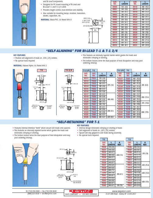
“SELF-ALIGNING”FOR BI-LEAD T-1&T-13/4and Bi-Lead components.•Designed for PC board mounting of Tri-Lead and Bi-Lead T-1and T-13/4LEDS •Provides height control,lead retention and stability.•Also suitable for mounting lamps,resistors,transistors,diodes,capacitors,etc.MATERIAL:Black PVC,UL Rated 94V-0•This features an internally tapered barrier which guides the leads and eliminates crimping or shorting.•The bottom bosses serve the dual purpose of heat dissipation and easy post soldering cleanup.FOR T-13/4and T-1CAT.L CAT.LNO.LENGTH NO.LENGTH 8900.120(3.0)8916.400(10.2)8901.140(3.6)8917.420(10.7)8902.160(4.1)8918.440(11.2)8903.180(4.6)8919.450(11.4)8904.200(5.1)8920.460(11.7)8905.220(5.6)8921.480(12.2)8906.240(6.1)8922.500(12.7)8907.250(6.4)8923.550(14.0)8908.260(6.6)8924.600(15.2)8909.280(7.1)8925.650(16.5)8910.300(7.6)8926.700(17.8)8911.320(8.1)8927.750(19.1)8912.340(8.6)8928.800(20.3)8913.350(8.9)8929.850(21.6)8914.360(9.1)8930.900(22.9)8915.380(9.7)8931.925(23.5)T-13/4T-1T-13/4T-1CAT.CAT.L A NO.NO.LENGTH REF.83117351.120(3.0)83127352.140(3.6)83137353.160(4.1).075(1.9)83147354.180(4.6)83157355.200(5.1)83167356.220(5.6)83177357.240(6.1)83187358.250(6.4)83197359260(6.6).190(4.8)83207360.280(7.1)83217361.300(7.6)83227362.320(8.1)83237363.340(8.6).200(5.1)83247364.350(8.9)83257365.360(9.1)83267366.380(9.7).325(8.3)T-13/4T-1CAT.CAT.L A NO.NO.LENGTH REF.83277367.400(10.2)83287368.420(10.7)83297369.440(11.2).325(8.3)83307370.450(11.4)83317371.460(11.7)83327372.480(12.2)83337373.500(12.7)83347374.550(14.0).450(11.4)83357375.600(15.2)83367376.650(16.5).575(14.6)83377377.700(17.8)83387378.750(19.1)83397379.800(20.3)83407380.850(21.6).690(17.5)83417381.900(22.9)83427382.925(23.5)Tel (718)956-8900•Fax (718)956-9040(800)221-5510•kec@31-0720th Road –Astoria,NY 11105-2017RoHS COMPLIANT ~ISO 9001CERTIFIED®KEY FEATURES•Positive self-alignment of leads on .100(.25)centers.•No special tools requiredMATERIAL:Natural Nylon,UL Rated 94V-2“SELF-RETAINING”FOR T-1.140[3.6]DIA..200[5.1]DIA..040[1.0]DIA.BOSSES (6)PLSLEAD RETAINING AND DRAINAGE.100[2.5].100[2.5].020[0.5]LA.033[0.84]DIA..040[1.02]x .065[1.65]SLOT (4)PLS L.255[6.5]DIA..208[5.3]TYP..093[2.4].133[3.4]DIA..100[2.5].045[1.1]DIA BOSSES (6)PLS..032[0.81]SQUARE [2]PLS.197[5.0]DIA.AL.020[0.5].045[1.1]DIA BOSSES (6)PLS..157[4.0]DIA..100[2.5].020[0.5].197[5.0]DIA.AL.032[0.81]SQUARE [2]PLST-1CAT.L A NO.LENGTH REF.7046.400(10.2)7047.420(10.7)7048.440(11.2)7049.450(11.4).310(7.9)7050.460(11.7)7051.480(12.2)7052.500(12.7)7053.550(14.0).435(11.0)7054.600(15.2)7055.650(16.5).650(14.2)7056.700(17.8)7057.750(19.1)7058.800(20.3)7059.850(21.6).690(17.5)7060.900(22.9)7061.925(23.5)T-1CAT.L A NO.LENGTH REF.7030.120(3.0)7031.140(3.6)7032.160(4.1)7033.180(4.6).060(1.5)7034.200(5.1)7035.220(5.6)7036.240(6.1)7037.250(6.4)7038.260(6.6)7039.280(7.1)7040.300(7.6).185(4.7)7041.320(8.1)7042.340(8.6)7043.350(8.9)7044.360(9.1)7045.380(9.7).310(7.9)•Features internal retention “teeth”which secure LED leads onto spacers.•This features an internally tapered barrier which guides the leads and eliminates crimping or shorting.•The bottom bosses serve the dual purpose of heat dissipation and easy post soldering cleanup.KEY FEATURES•Internal design eliminates crimping or shorting of leads •Self alignment of leads on .100[.25]centers.•Spacer will stay gripped to LED leads during assembly •No special tools required分销商库存信息:KEYSTONE-ELECTRONICS890073518904 735373558901 735473578907 736073568902 890373587363 736183137362 831583128318 832673707367 736589157366 737373748322 833383218323 833589258922 890673528327 891183208314 831783398334 735989088909 890583197364 736873697372 891089128913 891473717376 737783248328 832983318332 737873797380 738183368337 831683258311 738283388340 834183428916 891789188919 892089217375 833089238924 892689278928 892989308931。
3368-0000;3415-0000;3403-0000;中文规格书,Datasheet资料

PhysicalElectricalEnvironmental*"RoHS compliant" means that the product or part does not contain any of the following substances in excess of the following maximum concentrationvalues in any homogeneous material, unless the substance is in an application that is exempt under RoHS: (a) 0.1% (by weight) for lead, mercury,hexavalent chromium, polybrominated biphenyls or polybrominated diphenyl ethers; or (b) 0.01% (by weight) for cadmium. Unless otherwise stated by3M in writing, this information represents 3M's knowledge and belief based upon information provided by third party suppliers to 3M.InsulationMaterial:Glass Filled Polyester (PBT)Flammability:UL 94V-0Color:Gray Contact Material:Copper AlloyCover ClipMaterial:Stainless SteelPlatingUnderplating and U-Slot:100 μ″ [ 2.54 μm ] NickelWiping Area:30 μ″ [ 0.76 μm ] GoldWire Accommodation:26 and 28 AWG Solid and StrandedMarking:3M Logo, Part Identification Number and Position IdentificationCurrent Rating: 1 AInsulation Resistance:> 1 × 10⁹Ω at 500 V DC Withstanding Voltage:1000 V RMS at Sea LevelTemperature Rating:-55°C to +105°C•Standard drilled mounting flanges•Reinforced card-edge resists mouth bowing for consistent contact performance•Metal cover clips provide superior cover retention•Bifurcated contacts provide reliable contact with PC boards•Keying plug 3439-2 provides polarization and/or keying•RoHS* compliantTS-0012-12Sheet 1 of 3Date Modified: February 20, 2007UL File No.: E68080In ch[m m]T olerance U nless N oted.0.00.000 inch±.1±.01±.005[ ] D im ensions for R eferenceO nly Assembled3Important NoticeAll statements, technical information, and recommendationsrelated to 3M’s products are based on information believed to be reliable, but the accuracy or completeness is not guaranteed. Before using this product, you must evaluate it and determine if it is suitable for your intended application. You assume all risks and liability associated with such use. Any statements related to the product which are not contained in 3M’s current publications, or any contrary statements contained on your purchase order shall have no force or effect unless expressly agreed upon, in writing, by an authorized officer of 3M.Warranty; Limited Remedy; Limited Liability. This product will be free from defects in material and manufacture for a period of one (1) year from the time ofpurchase. 3M MAKES NO OTHER WARRANTIES INCLUDING, BUT NOT LIMITED TO, ANY IMPLIED WARRANTY OF MERCHANTABILITY OR FITNESS FOR A PARTICULARPURPOSE. If this product is defective within the warranty period stated above, your exclusive remedy shall be, at 3M’s option, to replace or repair the 3M product or refund the purchase price of the 3M product. Except where prohibited by law, 3M will not be liable for any indirect, special, incidental or consequential loss or damage arising from this 3M product, regardless of the legal theory asserted.3M Electronics6801 River Place Blvd.分销商库存信息:3M3368-00003415-00003403-0000。
0736443215;中文规格书,Datasheet资料

This document was generated on 08/09/2012PLEASE CHECK FOR LATEST PART INFORMATIONPart Number:73644-3215Status:ActiveOverview:HDM®Description:2.00mm Pitch HDM® Board-to-Board Backplane Header, Vertical, SMC, Press-Fit,Guide Post Location A, Polarizing Key Position H, 144 CircuitsDocuments:3D ModelRoHS Certificate of Compliance (PDF)Drawing (PDF)Agency CertificationCSA LR19980ULE29179GeneralProduct Family Backplane Connectors Series73644Application BackplaneCommentsStandard Press-Fit, Tin/Lead (SnPb)Component Type PCB Header OverviewHDM®Product Name HDM®Style N/AUPC800753302280PhysicalCircuits (Loaded)144Circuits (maximum)144Color - ResinBlack, Natural Durability (mating cycles max)250First Mate / Last Break No Flammability94V-0Guide to Mating Part Yes Keying to Mating Part YesMaterial - MetalPhosphor Bronze, Stainless Steel Material - Plating MatingGold Material - Plating Termination TinMaterial - Resin High Temperature Thermoplastic Number of Columns 24Number of Pairs Open Pin Field Number of Rows 6Orientation Vertical PC Tail Length 3.50mm PCB Locator No PCB RetentionYes PCB Thickness - Recommended 2.50mm Packaging TypeTube Pitch - Mating Interface2.00mm Pitch - Termination Interface 2.00mm Plating min - Mating0.762µm Plating min - Termination 0.381µm Polarized to PCB No StackableNo Surface Mount Compatible (SMC)YesTemperature Range - Operating -55°C to +105°CTermination Interface: StyleThrough Hole - Compliant PinSeriesimage - Reference onlyEU RoHSChina RoHSNot RoHS Compliant REACH SVHC Not ReviewedLow-Halogen Status Not ReviewedNeed more information on product environmental compliance?Email productcompliance@For a multiple part number RoHS Certificate of Compliance, click herePlease visit the Contact Us section for any non-product compliance questions.Search Parts in this Series 73644SeriesMates With73632 HDM PLUS® Board-to-Board Daughtercard Receptacle. 73780 HDM®Board-to-Board Daughtercard Receptacle Application Tooling | FAQTooling specifications and manuals are found by selecting the products below.Crimp Height Specifications are then contained in the Application Tooling Specification document.GlobalDescription Product #Extraction Tool 0621001000Backplane Insertion Signal Contact Tool0621001400Backplane Insertion Head for 144 Circuits0622005703Flat Rock Tooling for Pneumatic Press0622013700ElectricalCurrent - Maximum per Contact1AData Rate 1.0 GbpsReal Signals (per 25mm)75Shielded NoVoltage - Maximum250V ACMaterial InfoReference - Drawing NumbersSales Drawing SDA-73644-****HDM and High Density Metric are trademarks of Amphenol CorporationThis document was generated on 08/09/2012PLEASE CHECK FOR LATEST PART INFORMATION分销商库存信息: MOLEX 0736443215。
- 1、下载文档前请自行甄别文档内容的完整性,平台不提供额外的编辑、内容补充、找答案等附加服务。
- 2、"仅部分预览"的文档,不可在线预览部分如存在完整性等问题,可反馈申请退款(可完整预览的文档不适用该条件!)。
- 3、如文档侵犯您的权益,请联系客服反馈,我们会尽快为您处理(人工客服工作时间:9:00-18:30)。
Viewing Angle [1] 2θ1/2 60°
Typ. 100 40
50 White Diffused 20
Electrical / Optical Characteristics at TA=25°C
Symbol λpeak λD [1] Δλ1/2 C VF [2] IR Parameter Peak Wavelength Dominant Wavelength Spectral Line Half-width Capacitance Forward Voltage Reverse Current Device High Efficiency Red Yellow High Efficiency Red Yellow High Efficiency Red Yellow High Efficiency Red Yellow High Efficiency Red Yellow High Efficiency Red Yellow Typ. 627 590 625 588 45 35 15 20 2 2.1 2.5 2.5 10 10 Max. Units nm nm nm pF V uA Test Conditions IF=20mA IF=20mA IF=20mA VF=0V;f=1MHz IF=20mA VR = 5V
SPEC NO: DSAF2079 APPROVED: WYNEC
REV NO: V.3 CHECKED: Allen Liu
DATE: APR/08/2011 DRAWN: J.Yu
PAGE: 1 OF 6 ERP: 1102001744
/
Selection Guide
Package Dimensions
Notes: 1. All dimensions are in millimeters (inches). 2. Tolerance is ±0.25(0.01") unless otherwise noted. 3. Lead spacing is measured where the leads emerge from the package. 4. The specifications, characteristics and technical data described in the datasheet are subject to change without prior notice.
Notes: 1.Wavelength: +/-1nm. 2. Forward Voltage: +/-0.1V.
Absolute Maximum Ratings at TA=25°C
Parameter Power dissipation DC Forward Current Peak Forward Current [1] Reverse Voltage Operating / Storage Temperature Lead Solder Temperature [2] Lead Solder Temperature [3]
/
WP59CB/EYW High Efficiency Red
SPEC NO: DSAF2079 APPROVED: WYNEC
REV NO: V.3 CHECKED: Allen Liu
DATE: APR/08/2011 DRAWN: J.Yu
PAGE: 3 OF 6 ERP: 1102001744
Description
The High Efficiency Red source color devices are made with Gallium Arsenide Phosphide on Gallium Phosphide Orange Light Emitting Diode. The Yellow source color devices are made with Gallium Arsenide Phosphide on Gallium Phosphide Yellow Light Emitting Diode.
/
SPEC NO: DSAF2079 APPROVED: WYNEC
REV NO: V.3 CHECKED: Allen Liu
DATE: APR/08/2011 DRAWN: J.Yu
PAGE: 6 OF 6 ERP: 1102001744
/
/
Yellow
SPEC NO: DSAF2079 APPROVED: WYNEC
REV NO: V.3 CHECKED: Allen Liu
DATE: APR/08/2011 DRAWN: J.Yu
PAGE: 4 OF 6 ERP: 1102001744
/
-40°C To +85°C 260°C For 3 Seconds 260°C For 5 Seconds
SPEC NO: DSAF2079 APPROVED: WYNEC
REV NO: V.3 CHECKED: Allen Liu
DATE: APR/08/2011 DRAWN: J.Yu
PAGE: 2 OF 6 ERP: 1102001744
T-1 3/4 (5mm) BI-COLOR RIGHT ANGLE LED INDICATOR
Part Number: WP59CB/EYW High Efficiency Red Yellow
Features
z Pre-trimmed leads for pc board mounting. z 3 leads with one common lead. z Black case enhances contrast ratio. z Wide viewing angle. z High reliability - life measured in years. z Housing UL rating: 94V-0. z Housing material: type 66 nylon. z RoHS compliant.
PACKING & LABEL SPECIFICATIONS
WP59CB/EYW
SPEC NO: DSAF2079 APPROVED: WYNEC
REV NO: V.3 CHECKED: Allen Liu
DATE: APR/08/2011 DRAWN: J.Yu
PAGE: 5 OF 6 ERP: 1102001744
Notes: 1. 1/10 Duty Cycle, 0.1ms Pulse Width. 2. 2mm below package base. 3. 5mm below package base.
High Efficiency Red 75 30 160 5
Yellow 75 30 140
Units mW mA mA V
分销商库存信息:
KINGBRIGHT WP59CB/EYW
Part No. Dice Lens Type Iv (mcd) [2] @ 20mA Min. High Efficiency Red (GaAsP/GaP) WP59CB/EYW Yellow (GaAsP/GaP)
Notes: 1. θ1/2 is the angle from optical centerline where the luminous intensity is 1/2 of the optical peak value. 2. Luminous intensity/ luminous Flux: +/-15%.