IRF7201TRPBF;IRF7201PBF;中文规格书,Datasheet资料
IRLML2244TRPBF;中文规格书,Datasheet资料

1/24/111ORDERING INFORMATION:See detailed ordering and shipping information on the last page of this data sheet.Notes through are on page 10Features and BenefitsBenefitsApplication(s)• System/Load Switchresults in ⇒IRLML2244TRPbFIRLML2244TRPbF 3Fig 2. Typical Output CharacteristicsFig 1. Typical Output CharacteristicsFig 4. Normalized On-ResistanceVs. Temperature-V DS , Drain-to-Source Voltage (V)0.1110100-V DS , Drain-to-Source Voltage (V)-I D , D r a i n -t o -S o u r c e C u r r e n t (A )T J , Junction Temperature (°C)R D S (o n ) , D r a i n -t o -S o u r c e O n R e s i s t a n c eIRLML2244TRPbFFig 6. Typical Gate Charge Vs.Gate-to-Source VoltageFig 5. Typical Capacitance Vs.Drain-to-Source Voltage Fig 8. Maximum Safe Operating AreaFig 7. Typical Source-Drain DiodeForward Voltage110100-V DS , Drain-to-Source Voltage (V)10100100010000C , C a p a c i t a n c e (p F )-V SD , Source-to-Drain Voltage (V)0.1110100-I S D , R e v e r s e D r a i n C u r r e n t (A )110100-V DS , Drain-to-Source Voltage (V)0.010.1110100-I D , D r a i n -t o -S o u r c e C u r r e n t (A)048121620Q G, Total Gate Charge (nC)2468101214-V G S , G a t e -t o -S o u r c e V o l t a g e (V )IRLML2244TRPbF 5Fig 11. Typical Effective Transient Thermal Impedance, Junction-to-AmbientFig 9. Maximum Drain Current Vs.Ambient TemperatureFig 10b. Switching Time WaveformsFig 10a. Switching Time Test Circuit255075100125150T A , Ambient Temperature (°C)012345-I D , D r a i n C u r r e n t (A)t 1 , Rectangular Pulse Duration (sec)R DV DDV DSV t t t tFig 13. Typical On-Resistance Vs. DrainCurrentFig 12. Typical On-Resistance Vs. GateVoltageFig 14b. Gate Charge Test CircuitFig 14a. Basic Gate Charge Waveform 24681012-V GS, Gate -to -Source Voltage (V)20406080100120R D S (o n ), D r a i n -t o -S o u r c e O n R e s i s t a n c e (m Ω)5101520253035-I D , Drain Current (A)04080120160200R D S (o n ), D r a i n -t o -S o u r c e O n R e s i s t a n c e (m Ω)Vgs = -4.5VIdQgs1Qgs2Qgd Qgodr 0 7Fig 15. Typical Threshold Voltage Vs.Junction TemperatureFig 16. Typical Power Vs. TimeT J , Temperature ( °C )-V G S (t h ), G a t e t h r e s h o l d V o l t a g e (V )Time (sec)P o w e r (W )IRLML2244TRPbFMicro3 (SOT-23/TO-236AB) Part Marking InformationMicro3 (SOT-23) Package OutlineDimensions are shown in millimeters (inches)Note: For the most current drawing please refer to IR website at: /package/cF =DA T E C E =X = D =C =B =A =W = (1-26) IF PRECEDED BY LAST DIG IT O F C ALENDA R YEA RH =G =KH G F E D C B 200620032002200520042008200720102009J Y 51292830C B D52ZNote: A line a bove the work we e k(a s s how n he re ) indic a tes Le a d - Fre e.I =J = IRLML2030L = IRLML0060M = IRLML0040K = IRLML0100N = IRLML2060P = IRLML9301R = IRLML9303C u HALOG PAIRLML2244TRPbF 9Micro3™ Tape & Reel InformationDimensions are shown in millimeters (inches)2.05 ( .080 )1.95 ( .077 )TRFEED DIRECTION4.1 ( .161 )3.9 ( .154 )1.6 ( .062 )1.5 ( .060 )1.85 ( .072 )1.65 ( .065 )3.55 ( .139 )3.45 ( .136 )1.1 ( .043 )0.9 ( .036 )4.1 ( .161 )3.9 ( .154 )0.35 ( .013 )0.25 ( .010 )8.3 ( .326 )7.9 ( .312 )1.32 ( .051 )1.12 ( .045 )9.90 ( .390 )8.40 ( .331 )178.00( 7.008 ) MAX.NOTES:1. CONTROLLING DIMENSION : MILLIMETER.2. OUTLINE CONFORMS TO EIA-481 & EIA-541.Note: For the most current drawing please refer to IR website at: /package/IRLML2244TRPbFData and specifications subject to change without notice.IR WORLD HEADQUARTERS: 233 Kansas St., El Segundo, California 90245, USA Tel: (310) 252-7105TAC Fax: (310) 252-7903Visit us at for sales contact information .01/2011Qualification standards can be found at International Rectifier’s web site /product-info/reliabilityHigher qualification ratings may be available should the user have such requirements. Please contact your International Rectifier sales representative for further information: /whoto-call/salesrep/Applicable version of JEDEC standard at the time of product release.Notes:Repetitive rating; pulse width limited by max. junction temperature. Pulse width ≤ 400μs; duty cycle ≤ 2%. Surface mounted on 1 in square Cu board Refer to application note #AN-994.Qualification information †分销商库存信息: IRIRLML2244TRPBF。
IR公司_大功率MOS管选型

I DContinuous Drain Current(A)70°Micro3Surface Mount PackagesV (BR)DSSDrain-to-Source Breakdown Voltage (V)R DS(on)On-State Resistance ()ΩI D Continuous Drain Current 25°C(A)R ΘMax.Thermal Resistance (°C/W)1FaxonDemand Number Case Outline KeyPartNumberPD Max.PowerDissipation (W)N-ChannelLogic LevelIRLML2402*912570.54200.25 1.20.95230H1IRLML2803912580.54300.251.20.93230P-ChannelLogic LevelIRLML6302*912590.54-200.6-0.62-4.8230H1IRLML5103912600.54-300.6-0.61-4.8230* Indicates low VGS(th), which can operate at VGS = 2.7VMeasured at ambient for Micro3, Micro6, Micro8, SO-8, and SOT-223 package styles. All others measured at case.1Micro3SO-8D-PakD -PakSOT-227Micro6SOT-223Micro82 Illustrations not to scaleI DContinuous Drain Current(A)70°Micro6Surface Mount PackagesV (BR)DSSDrain-to-Source Breakdown Voltage (V)R DS(on)On-State Resistance ()ΩI D Continuous Drain Current 25°C(A)R ΘMax.Thermal Resistance (°C/W)1FaxonDemand Number Case Outline KeyPartNumberPD Max.PowerDissipation (W)N-ChannelLogic LevelIRLMS1902915401.7200.10 3.2 2.675H2IRLMS1503915081.7300.103.22.675P-ChannelLogic LevelIRLMS6702*914141.7-200.20-2.3-1.975H2IRLMS5703914131.7-300.20-2.3-1.975* Indicates low VGS(th), which can operate at VGS = 2.7VMeasured at ambient for Micro3, Micro6, Micro8, SO-8, and SOT-223 package styles. All others measured at case.1Micro3SO-8D-PakD -PakSOT-227Micro6SOT-223Micro82 Illustrations not to scaleI DContinuous Drain Current(A)70°Micro8Surface Mount PackagesV (BR)DSSDrain-to-Source Breakdown Voltage (V)R DS(on)On-State Resistance ()ΩI D Continuous Drain Current 25°C(A)R ΘMax.Thermal Resistance (°C/W)1FaxonDemand Number Case Outline KeyPart NumberP D Max.PowerDissipation (W)N-Channel Logic LevelIRF7601* 912611.820 0.035 5.7 4.6 70 H3IRF7603 912621.830 0.035 5.6 4.5 70Dual N-Channel Logic LevelIRF7501* 912651.220 0.135 2.4 1.9 100 H3IRF7503 912661.2530 0.135 2.4 1.9 100P-Channel Logic LevelIRF7604* 912631.8-20 0.09 -3.6 -2.9 70 H3IRF7606 912641.8-30 0.09 -3.6 -2.9 70Dual P-Channel Logic LevelIRF7504* 912671.25-20 0.27 -1.7 -1.4 100 H3IRF7506 912681.25-30 0.27 -1.7 -1.4 100Dual N- and P-Channel Logic LevelIRF7507* 912691.2520 0.1352.4 1.9 100 H3-20 0.27 -1.7 -1.4IRF7509 912701.2530 0.135 2.4 1.9 100-30 0.27 -1.7 -1.4* Indicates low VGS(th), which can operate at VGS = 2.7VMeasured at ambient for Micro3, Micro6, Micro8, SO-8, and SOT-223 package styles. All others measured at case.1Micro3SO-8D-Pak D -PakSOT-227Micro6SOT-223Micro8 2 Illustrations not to scaleI DContinuous Drain Current(A)70°SO-8Surface Mount PackagesV (BR)DSSDrain-to-Source Breakdown Voltage (V)R DS(on)On-State Resistance ()ΩI D Continuous Drain Current 25°C(A)R ΘMax.Thermal Resistance (°C/W)1FaxonDemand Number Case Outline KeyPart Number P D Max.PowerDissipation (W)N-ChannelIRF7413913302.5300.011139.250H4IRF7413A 916132.5300.0135128.450IRF9410915622.5300.0375.850Dual N-ChannelIRF7311914352.0200.029 6.6 5.362.5H4IRF7313914802.0300.029 6.5 5.262.5IRF7333917002.0300.10 3.5 2.862.5917002.0300.050 4.9 3.962.5IRF9956915592.0300.103.52.862.5Dual P-ChannelIRF7314914352.0-200.058-5.3-4.362.5H4IRF7316915052.0-300.058-4.9-3.962.5IRF9953915602.0-300.25-2.3-1.862.5* Indicates low VGS(th), which can operate at VGS = 2.7VMeasured at ambient for Micro3, Micro6, Micro8, SO-8, and SOT-223 package styles. All others measured at case.1Micro3SO-8D-PakD -PakSOT-227Micro6SOT-223Micro82 Illustrations not to scaleI DContinuous Drain Current(A)70°SO-8Surface Mount PackagesV (BR)DSSDrain-to-Source Breakdown Voltage (V)R DS(on)On-State Resistance ()ΩI D Continuous Drain Current 25°C(A)RΘMax.ThermalResistance(°C/W)1FaxonDemand Number Case Outline KeyPart NumberP D Max.PowerDissipation (W)Dual N- and P-ChannelIRF7317 915682.020 0.029 6.6 5.3 62.5 H42.0-20 0.058 -5.3 -4.3 62.5IRF9952 915622.030 0.103.5 2.8 62.5915622.0-30 0.25 -2.3 -1.8 62.5IRF7319 916062.030 0.029 6.5 5.2 62.52.0-30 0.058 -4.9 -3.9 62.5* Indicates low VGS(th), which can operate at VGS = 2.7VMeasured at ambient for Micro3, Micro6, Micro8, SO-8, and SOT-223 package styles. All others measured at case.1Micro3SO-8D-Pak D -PakSOT-227Micro6SOT-223Micro8 2 Illustrations not to scaleI DContinuous Drain Current(A)70°SO-8Surface Mount PackagesV (BR)DSSDrain-to-Source Breakdown Voltage (V)R DS(on)On-State Resistance ()ΩI D Continuous Drain Current 25°C(A)R ΘMax.Thermal Resistance (°C/W)1FaxonDemand Number Case Outline KeyPart Number P D Max.PowerDissipation (W)N-ChannelLogic LevelIRF7401912442.5200.0228.77.050H4IRF7201911002.5300.0307.0 5.650IRF7403912452.5300.0228.55.450Dual N-ChannelLogic LevelIRF7101908712.0200.10 3.5 2.362.5H4IRF7301912382.0200.050 5.2 4.162.5IRF7303912392.0300.050 4.9 3.962.5IRF7103910952.0500.1303.02.362.5P-ChannelLogic LevelIRF7204911032.5-200.060-5.3-4.250H4IRF7404912462.5-200.040-6.7-5.450IRF7205911042.5-300.070-4.6-3.750IRF7406912472.5-300.045-5.8-3.750IRF7416913562.5-300.02-10-7.150* Indicates low VGS(th), which can operate at VGS = 2.7VMeasured at ambient for Micro3, Micro6, Micro8, SO-8, and SOT-223 package styles. All others measured at case.1Micro3SO-8D-PakD -PakSOT-227Micro6SOT-223Micro82 Illustrations not to scaleI DContinuous Drain Current(A)70°SO-8Surface Mount PackagesV (BR)DSSDrain-to-Source Breakdown Voltage (V)R DS(on)On-State Resistance ()ΩI D Continuous Drain Current 25°C(A)R ΘMax.Thermal Resistance (°C/W)1FaxonDemand Number Case Outline KeyPart Number P D Max.PowerDissipation (W)Dual P-ChannelLogic LevelIRF7104910962.0-200.250-2.3-1.862.5H4IRF7304912402.0-200.090-4.3-3.462.5IRF7306912412.0-300.10-3.6-2.962.5Dual N- and P-Channe Logic LevelIRF7307912421.4200.050 4.3 3.490H4-200.090-3.6-2.9IRF7105910972.0250.1093.5 2.862.52-250.25-2.3-1.862IRF7309912432.0300.050 4.9 3.962.5-300.10-3.6-2.9* Indicates low VGS(th), which can operate at VGS = 2.7VMeasured at ambient for Micro3, Micro6, Micro8, SO-8, and SOT-223 package styles. All others measured at case.1Micro3SO-8D-PakD -PakSOT-227Micro6SOT-223Micro82 Illustrations not to scaleI DContinuous Drain Current(A)70°SOT-223Surface Mount PackagesV (BR)DSSDrain-to-Source Breakdown Voltage (V)R DS(on)On-State Resistance ()ΩI D Continuous Drain Current 25°C(A)R ΘMax.Thermal Resistance (°C/W)1FaxonDemand Number Case Outline KeyPart Number P D Max.PowerDissipation (W)N-ChannelIRFL4105913812.1550.045 3.7 3.060H6IRFL110908612.01000.54 1.50.9660IRFL4310913682.11000.20 1.6 1.360IRFL21090868 2.02001.50.960.660IRFL214908622.02502.00.790.560P-ChannelIRFL9110908642.0-1001.2-1.1-0.6960H6N-ChannelLogic LevelIRLL3303913792.1300.031 4.6 3.760H6IRLL014N 914992.1550.14 2.0 1.660IRLL2705913802.1550.043.83.060* Indicates low VGS(th), which can operate at VGS = 2.7VMeasured at ambient for Micro3, Micro6, Micro8, SO-8, and SOT-223 package styles. All others measured at case.1Micro3SO-8D-PakD -PakSOT-227Micro6SOT-223Micro82 Illustrations not to scaleI DContinuous Drain Current(A)100°D-PakSurface Mount PackagesV (BR)DSSDrain-to-Source Breakdown Voltage (V)R DS(on)On-State Resistance ()ΩI D Continuous Drain Current 25°C(A)R ΘMax.Thermal Resistance (°C/W)1FaxonDemand Number Case Outline KeyPart Number P D Max.PowerDissipation (W)N-ChannelIRFR33039164257300.0313321 2.2H7IRFR024N9133638550.0751610 3.3IRFR41059130248550.0452516 2.7IRFR12059131869550.0273723 1.8IRFR11090524251000.54 4.3 2.75IRFR120N 91365391000.219.1 5.8 3.2IRFR391091364521000.11159.5 2.4IRFR2109052625200 1.5 2.6 1.75IRFR22090525422000.8 4.833IRFR21490703252502 2.2 1.45IRFR2249060042250 1.1 3.8 2.43IRFR3109059725400 3.6 1.7 1.15IRFR3209059842400 1.8 3.123IRFR42090599425003 2.4 1.53IRFRC2090637426004.421.33* Indicates low VGS(th), which can operate at VGS = 2.7VMeasured at ambient for Micro3, Micro6, Micro8, SO-8, and SOT-223 package styles. All others measured at case.1Micro3SO-8D-PakD -PakSOT-227Micro6SOT-223Micro82 Illustrations not to scaleI DContinuous Drain Current(A)100°D-PakSurface Mount PackagesV (BR)DSSDrain-to-Source Breakdown Voltage (V)R DS(on)On-State Resistance ()ΩI D Continuous Drain Current 25°C(A)R ΘMax.Thermal Resistance (°C/W)1FaxonDemand Number Case Outline KeyPart Number P D Max.PowerDissipation (W)P-ChannelIRFR55059161057-550.11-18-11 2.2H7IRFR53059140289-550.065-28-18 1.4IRFR90149065425-600.5-5.1-3.25IRFR90249065542-600.28-8.8-5.63IRFR91109051925-100 1.2-3.1-25IRFR91209052042-1000.6-5.6-3.63IRFR9120N 9150739-1000.48-6.5-4.1 3.2IRFR92109052125-2003-1.9-1.25IRFR92209052242-200 1.5-3.6-2.33IRFR92149165850-250 3.0-2.7-1.7 2.5IRFR93109166350-4007.0-1.8-1.12.5* Indicates low VGS(th), which can operate at VGS = 2.7VMeasured at ambient for Micro3, Micro6, Micro8, SO-8, and SOT-223 package styles. All others measured at case.1Micro3SO-8D-PakD -PakSOT-227Micro6SOT-223Micro82 Illustrations not to scaleI DContinuous Drain Current(A)100°D-PakSurface Mount PackagesV (BR)DSSDrain-to-Source Breakdown Voltage (V)R DS(on)On-State Resistance ()ΩI D Continuous Drain Current 25°C(A)R ΘMax.Thermal Resistance (°C/W)1FaxonDemand Number Case Outline KeyPart Number P D Max.PowerDissipation (W)N-ChannelLogic LevelIRLR27039133538300.0452214 3.3H7IRLR33039131657300.0313321 2.2IRLR31039133369300.0194629 1.8IRLR024N 9136338550.0651711 3.3IRLR27059131746550.042415 2.7IRLR29059133469550.0273623 1.8IRLR120N 91541391000.18511 6.9 3.2IRLR341091607521000.10159.52.4* Indicates low VGS(th), which can operate at VGS = 2.7VMeasured at ambient for Micro3, Micro6, Micro8, SO-8, and SOT-223 package styles. All others measured at case.1Micro3SO-8D-PakD -PakSOT-227Micro6SOT-223Micro82 Illustrations not to scaleI DContinuous Drain Current(A)100°D 2PakSurface Mount PackagesV (BR)DSSDrain-to-Source Breakdown Voltage (V)R DS(on)On-State Resistance ()ΩI D Continuous Drain Current 25°C(A)R ΘMax.Thermal Resistance (°C/W)1FaxonDemand Number Case Outline KeyPart NumberP D Max.PowerDissipation (W)N-ChannelIRFZ24NS 913554555 0.07 17 12 3.3 H10IRFZ34NS 913116855 0.04 29 20 2.2IRFZ44NS 9131511055 0.022 49 35 1.4IRFZ46NS 9130512055 0.020 53 37 1.3IRFZ48NS 9140814055 0.016 64 45 1.1IRF1010NS 913723.855 0.011 84 60 40IRF3205S 9130420055 0.008 110 80 0.75IRFZ44ES 9171411060 0.023 48 34 1.4IRF1010ES 9172017060 0.012 83 59 0.90IRF2807S 9151815075 0.013 71 50 1.0IRF520NS 9134047100 0.2 9.5 6.7 3.2IRF530NS 9135263100 0.11 15 11 2.4IRF540NS 91342110100 0.052 27 19 1.6IRF1310NS 91514120100 0.036 36 25 1.3IRF3710S 91310150100 0.028 46 33 1.0IRF3315S 9161794150 0.082 21 15 1.6IRF3415S 91509150150 0.042 37 26 1.0IRFBC20S 9.101450600 4.4 2.2 1.4 2.5IRFBC30S 9101574600 2.2 3.6 2.3 1.7IRFBC40S 91016130600 1.2 6.2 3.9 1.0* Indicates low VGS(th), which can operate at VGS = 2.7VMeasured at ambient for Micro3, Micro6, Micro8, SO-8, and SOT-223 package styles. All others measured at case.1Micro3SO-8D-Pak D -PakSOT-227Micro6SOT-223Micro8 2 Illustrations not to scaleI DContinuous Drain Current(A)100°D 2PakSurface Mount PackagesV (BR)DSSDrain-to-Source Breakdown Voltage (V)R DS(on)On-State Resistance ()ΩI D Continuous Drain Current 25°C(A)R ΘMax.Thermal Resistance (°C/W)1FaxonDemandNumberCase Outline KeyPart NumberP D Max.PowerDissipation (W)IRFBF20S 9166554900 8.0 1.7 1.1 2.3 H10P-ChannelIRF5305S 91386110-55 0.06 -31 -22 1.4 H10IRF4905S 914783.8-55 0.02 -74 -52 40IRF9520NS 9152247-100 0.48 -6.7 -4.8 3.2IRF9530NS 9152375-100 0.20 -14 -9.9 2.0IRF9540NS 9148394-100 0.117 -19 -13 1.6IRF5210S 91405150-100 0.06 -35 -25 1.0* Indicates low VGS(th), which can operate at VGS = 2.7VMeasured at ambient for Micro3, Micro6, Micro8, SO-8, and SOT-223 package styles. All others measured at case.1Micro3SO-8D-Pak D -PakSOT-227Micro6SOT-223Micro8 2 Illustrations not to scaleI DContinuous Drain Current(A)100°D 2PakSurface Mount PackagesV (BR)DSSDrain-to-Source Breakdown Voltage (V)R DS(on)On-State Resistance ()ΩI D Continuous Drain Current 25°C(A)R ΘMax.Thermal Resistance (°C/W)1FaxonDemand Number Case Outline KeyPart NumberP D Max.PowerDissipation (W)N-Channel Logic LevelIRL3302S 916925720 0.020 39 25 2.2 H10IRL3202S916756920 0.016 48 30 1.8IRL3102S 916918920 0.013 61 39 1.4IRL3402S 9169311020 0.01 85 54 1.1IRL3502S 9167614020 0.007 110 67 0.89IRL2703S 913604530 0.04 24 17 3.3IRL3303S 913236830 0.026 38 27 2.2IRL3103S 9133811030 0.014 64 45 1.4IRL2203NS 9136717030 0.007 116 82 0.90IRL3803S 9131920030 0.006 140 98 0.75IRLZ24NS 913584555 0.06 18 13 3.3IRLZ34NS 913086855 0.035 30 21 2.2IRLZ44NS 9134711055 0.022 47 33 1.4IRL3705NS 9150217055 0.01 89 63 0.90IRL2505S 9132620055 0.008 104 74 0.75IRLZ44S 9090615060 0.028 50 36 1.0IRL530NS 9134963100 0.1 15 11 2.4IRL2910S 91376150100 0.026 48 34 1.0* Indicates low VGS(th), which can operate at VGS = 2.7VMeasured at ambient for Micro3, Micro6, Micro8, SO-8, and SOT-223 package styles. All others measured at case.1Micro3SO-8D-Pak D -PakSOT-227Micro6SOT-223Micro8 2 Illustrations not to scaleI DContinuous Drain Current(A)100°SOT-227Surface Mount PackagesV (BR)DSSDrain-to-Source Breakdown Voltage (V)R DS(on)On-State Resistance ()ΩI D Continuous DrainCurrent 25°C(A)RΘMax.Thermal Resistance (°C/W)1FaxonDemand Number Case Outline KeyPart Number P D Max.PowerDissipation (W)N-ChannelFully Isolated Low ChargeFA38SA50LC 916155005000.1338240.25H21FA57SA50LC916506255000.0857360.20* Indicates low VGS(th), which can operate at VGS = 2.7VMeasured at ambient for Micro3, Micro6, Micro8, SO-8, and SOT-223 package styles. All others measured at case.1Micro3SO-8D-PakD -PakSOT-227Micro6SOT-223Micro82 Illustrations not to scaleI DContinuous Drain Current(A)100°I-PakThrough-Hole PackagesV (BR)DSSDrain-to-Source Breakdown Voltage (V)R DS(on)On-State Resistance ()ΩI D Continuous Drain Current 25°C(A)R ΘMax.Thermal Resistance (°C/W)1FaxonDemand Number Case Outline KeyPart Number P D Max.PowerDissipation (W)N-ChannelIRFU33039164257300.0313321 2.2H8IRFU024N 9133638550.0751610 3.3IRFU41059130248550.0452519 2.7IRFU12059131869550.0273723 1.8IRFU11090524251000.54 4.3 2.7 5.0IRFU120N 91365391000.219.1 5.8 3.2IRFU391091364521000.11159.5 2.4IRFU2109052625200 1.5 2.6 1.7 5.0IRFU22090525422000.80 4.8 3.0 3.0IRFU2149070325250 2.0 2.2 1.4 5.0IRFU2249060042250 1.1 3.8 2.4 3.0IRFU3109059725400 3.6 1.7 1.1 5.0IRFU3209059842400 1.8 3.1 2.0 3.0IRFU4209059942500 3.0 2.4 1.5 3.0IRFUC2090637426004.42.01.33.0I-PakTO-220 FullPakTO-262TO-247HEXDIPTO-220AB Illustrations not to scale** Not ratedI DContinuous Drain Current(A)100°I-PakThrough-Hole PackagesV (BR)DSSDrain-to-Source Breakdown Voltage (V)R DS(on)On-State Resistance ()ΩI D Continuous Drain Current 25°C(A)R ΘMax.Thermal Resistance (°C/W)1FaxonDemand Number Case Outline KeyPart Number P D Max.PowerDissipation (W)P-ChannelIRFU55059161057-550.11-18-11 2.2H8IRFU53059140289-550.065-28-18 1.4IRFU90149065425-600.50-5.1-3.2 5.0IRFU90249065542-600.28-8.8-5.6 3.0IRFU91109051925-100 1.2-3.1-2.0 5.0IRFU91209052042-1000.60-5.6-3.6 3.0IRFU9120N 9150739-1000.48-6.5-4.1 3.2IRFU92109052125-200 3.0-1.9-1.2 5.0IRFU92209052242-200 1.5-3.6-2.3 3.0IRFU92149165850-2503.0-2.7-1.7 2.5IRFU93109166350-4007.0-1.8-1.12.5N-ChannelLogic LevelIRLU27039133538300.0452214 3.3H8IRLU33039131657300.0313321 2.2IRLU31039133369300.0194629 1.8IRLU024N 9136338550.0651711 3.3IRLU27059131746550.04241715IRLU29059133469550.0273623 1.8IRLU120N 91541391000.18511 6.9 3.2IRLU341091607521000.10159.52.4I-PakTO-220 FullPakTO-262TO-247HEXDIPTO-220AB Illustrations not to scale** Not ratedI DContinuous Drain Current(A)100°HEXDIPThrough-Hole PackagesV (BR)DSSDrain-to-Source Breakdown Voltage (V)R DS(on)On-State Resistance ()ΩI D Continuous Drain Current 25°C(A)R ΘMax.Thermal Resistance (°C/W)1FaxonDemand Number Case Outline KeyPart Number P D Max.PowerDissipation (W)N-ChannelIRFD014907001.3600.2 1.7 1.2120H9IRFD024906991.3600.1 2.5 1.8120IRFD110903281.31000.54 1.00.71120IRFD120903851.31000.27 1.30.94120IRFD210903861.3200 1.50.60.38120IRFD220904171.32000.80.80.50120IRFD214912711.3250 2.00.570.32120IRFD224912721.3250 1.10.760.43120IRFD310912251.3400 3.60.420.23120IRFD320912261.3400 1.80.600.33120IRFD420912271.3500 3.00.460.26120IRFDC20912281.36004.40.320.21120I-PakTO-220 FullPakTO-262TO-247HEXDIPTO-220AB Illustrations not to scale** Not ratedI D Continuous Drain Current (A)100°TO-220Qg TotalGate Charge(nC)Through-Hole PackagesV (BR)DSSDrain-to-Source Breakdown Voltage (V)R DS(on)On-State Resistance ()ΩI D Continuous Drain Current 25°C (A)R ΘMax.Thermal Resistance(°C/W)1Faxon Demand Number Case OutlineKeyPart Number P D Max.Power Dissipation (W)N-ChannelLow ChargeIRF737LC91314743000.75 6.1** 1.7 3.9H11IRF740LC 910681254000.5510** 1.039IRF840LC 910691255000.858.0** 1.039IRFBC40LC910701256001.26.2**1.039I-PakTO-220 FullPakTO-262TO-247HEXDIPTO-220AB Illustrations not to scale** Not ratedI DContinuous Drain Current(A)100°TO-220ABThrough-Hole PackagesV (BR)DSSDrain-to-Source Breakdown Voltage (V)R DS(on)On-State Resistance ()ΩI D Continuous Drain Current 25°C(A)R ΘMax.Thermal Resistance (°C/W)1FaxonDemand Number Case Outline KeyPart Number P D Max.PowerDissipation (W)N-ChannelIRFZ24N 9135445550.071712 3.3H12IRFZ34N9127656550.042618 2.7IRFZ44N 9130383550.0244129 1.8IRFZ46N 9127788550.024633 1.7IRFZ48N 9140694550.0165337 1.6IRF1010N 91278130550.0127251 1.2IRF320591279150550.0089869 1.0IRFZ34E 9167268600.0422820 2.2IRFZ44E 91671110600.0234834 1.4IRF1010E 91670170600.01281570.90IRF280791517150750.0137150 1.0IRF520N 91339471000.209.5 6.79.5IRF530N 91351601000.111511 2.4IRF540N 91341941000.0522719 1.6IRF1310N 916111201000.0363625 1.3IRF3710913091501000.0284633 1.0IRF331591623941500.0822115 1.6IRF3415914771501500.0423726 1.0IRFBC209062350600 4.4 2.2 1.4 2.5IRFBC309048274600 2.2 3.6 2.3 1.7IRFBC4090506125600 1.2 6.2 3.9 1.0IRFBE2090610548006.51.81.22.3I-PakTO-220 FullPakTO-262TO-247HEXDIPTO-220AB Illustrations not to scale** Not ratedI DContinuous Drain Current(A)100°TO-220ABThrough-Hole PackagesV (BR)DSSDrain-to-Source Breakdown Voltage (V)R DS(on)On-State Resistance ()ΩI D Continuous Drain Current 25°C(A)R ΘMax.Thermal Resistance (°C/W)1FaxonDemand Number Case Outline KeyPart Number P D Max.PowerDissipation (W)IRFBE3090613125800 3.0 4.1 2.6 2.0H12IRFBF3090616125900 3.7 3.6 2.3 1.0IRFBG209060454100011 1.40.86 2.3IRFBG309062012510005.03.12.01.0P-ChannelIRF9Z24N 9148445-550.175-12-8.53.3H12IRF9Z34N 9148556-550.10-17-12 2.7IRF530591385110-550.06-31-22 1.4IRF490591280150-550.02-64-45 1.0IRF9530N 9148275-1000.20-13-9.2 2.0IRF9540N 9143794-1000.117-19-13 1.6IRF521091434150-1000.06-35-25 1.0IRF62159147983-1500.29-11-7.81.8I-PakTO-220 FullPakTO-262TO-247HEXDIPTO-220AB Illustrations not to scale** Not ratedI DContinuous Drain Current(A)100°TO-220ABThrough-Hole PackagesV (BR)DSSDrain-to-Source Breakdown Voltage (V)R DS(on)On-State Resistance ()ΩI D Continuous Drain Current 25°C(A)R ΘMax.Thermal Resistance (°C/W)1FaxonDemand Number Case Outline KeyPart NumberP D Max.PowerDissipation (W)N-Channel Logic LevelIRL3302 916965720 0.020 39 25 2.2 H12IRL3202 916956920 0.016 48 30 1.8IRL3102 916948920 0.013 61 39 1.4IRL3402 9169711020 0.01 85 54 1.1IRL3502 9169814020 0.007 110 67 0.89IRL2703 913594530 0.04 24 17 3.3IRL3303 913225630 0.026 34 24 2.7IRL3103 913378330 0.014 56 40 1.8IRL2203N 9136613030 0.007 100 71 1.230 0.007 61 43 3.2IRL3803 9130115030 0.006 120 83 1.0IRLZ24N 913574555 0.06 18 13 3.3IRLZ34N 913075655 0.035 27 19 2.7IRLZ44N 913468355 0.022 41 29 1.8IRL3705N 9137013055 0.01 77 54 1.2IRL2505 9132520055 0.008 104 74 0.75IRL520N 9149447100 0.18 10 7.1 3.2IRL530N 9134863100 0.10 15 11 2.4IRL540N 9149594100 0.044 30 21 1.6IRL2910 91375150100 0.026 48 34 1.0I-PakTO-220 FullPakTO-262TO-247HEXDIPTO-220AB Illustrations not to scale** Not ratedI D Continuous Drain Current (A)100°TO-220 FullPak (Fully Isolated)Qg TotalGate Charge(nC)Through-Hole PackagesV (BR)DSSDrain-to-Source Breakdown Voltage (V)R DS(on)On-State Resistance ()ΩI D Continuous DrainCurrent 25°C(A)R ΘMax.Thermal Resistance (°C/W)1Fax on Demand Number Case OutlineKeyPart Number P D Max.Power Dissipation (W)N-ChannelLow ChargeIRFI740GLC91209404000.55 6.0** 3.139H13IRFI840GLC 91208405000.85 4.8** 3.139IRFIBC40GLC91211406001.24.0**3.139I-PakTO-220 FullPakTO-262TO-247HEXDIPTO-220AB Illustrations not to scale** Not ratedI DContinuous Drain Current(A)100°TO-220 FullPak (Fully Isolated)Through-Hole PackagesV (BR)DSSDrain-to-Source Breakdown Voltage (V)R DS(on)On-State Resistance ()ΩI D Continuous Drain Current 25°C(A)R ΘMax.Thermal Resistance (°C/W)1FaxonDemand Number Case Outline KeyPart Number P D Max.PowerDissipation (W)N-ChannelIRFIZ24N 9150126550.07139.2 5.8H14IRFIZ34N9148931550.041913 4.8IRFIZ44N 9140338550.02428200.024IRFIZ46N 9130640550.023122 3.8IRFIZ48N 9140742550.0163625 3.6IRFI1010N 9137347550.0124431 3.2IRFI32059137448550.0085640 3.1IRFIZ24E 9167329600.071149.6 5.2IRFIZ34E 9167437600.0422115 4.1IRFI510G 90829271000.54 4.5 3.2 5.5IRFI520N 91362271000.207.2 5.1 5.5IRFI530N 91353331000.11117.8 4.5IRFI540N 91361421000.0521813 3.6IRFI1310N 91611451000.0362216 3.3IRFI371091387481000.0252820 3.1IRFI620G 90832302000.8 4.1 2.6 4.1IRFI630G 90652322000.4 5.9 3.7 3.6IRFI640G 90649402000.189.8 6.2 3.1IRFI614G 9083123250 2.0 2.1 1.3 5.5IRFI624G 9083330250 1.1 3.4 2.2 4.1IRFI634G 90738322500.45 5.6 3.5 3.6IRFI644G 90739402500.287.953.1I-PakTO-220 FullPakTO-262TO-247HEXDIPTO-220AB Illustrations not to scale** Not ratedI DContinuous Drain Current(A)100°TO-220 FullPak (Fully Isolated)Through-Hole PackagesV (BR)DSSDrain-to-Source Breakdown Voltage (V)R DS(on)On-State Resistance ()ΩI D Continuous Drain Current 25°C(A)R ΘMax.Thermal Resistance (°C/W)1FaxonDemand Number Case Outline KeyPart Number P D Max.PowerDissipation (W)IRFI720G 9083430400 1.8 2.6 1.7 4.1H14IRFI730G 9065032400 1.0 3.7 2.3 3.6IRFI740G 90651404000.55 5.4 3.4 3.1IRFI734G 9100135450 1.2 3.4 2.1 3.6IRFI744G 91002404500.63 4.9 3.1 3.1IRFI820G 9064130500 3.0 2.1 1.3 4.1IRFI830G 9064632500 1.5 3.12 3.6IRFI840G 90642405000.85 4.6 2.9 3.1IRFIBC20G 90850306004.41.71.1 4.1IRFIBC30G 90851356002.2 2.5 1.63.6IRFIBC40G 9085240600 1.2 3.5 2.2 3.1IRFIBE20G 9085330800 6.5 1.4.86 4.1IRFIBE30G 9085435800 3.0 2.1 1.4 3.6IRFIBF20G 90855309008.0 1.2.79 4.1IRFIBF30G90856359003.71.91.23.6P-ChannelIRFI9Z24N 9152929-550.175-9.5-6.7 5.2H14IRFI9Z34N 9153037-550.10-14-10 4.1IRFI49059152663-550.02-41-29 2.4IRFI9540G 9083742-1000.117-13-9.2 3.6IRFI9540N 9148742-1000.117-13-9.2 3.6IRFI52109140448-1000.06-20-14 3.1IRFI9634G 9148835-2501.0-4.1-2.63.6I-PakTO-220 FullPakTO-262TO-247HEXDIPTO-220AB Illustrations not to scale** Not ratedI DContinuous Drain Current(A)100°TO-220 FullPak (Fully Isolated)Through-Hole PackagesV (BR)DSSDrain-to-Source Breakdown Voltage (V)R DS(on)On-State Resistance ()ΩI D Continuous Drain Current 25°C(A)R ΘMax.Thermal Resistance (°C/W)1FaxonDemand Number Case Outline KeyPart Number P D Max.PowerDissipation (W)N-ChannelLogic LevelIRLI2203N 9137847300.0076143 3.2H14IRLI38039132048300.0066747 3.1IRLIZ24N 9134426550.06149.9 5.8IRLIZ34N 9132931550.0352014 4.8IRLIZ44N 9149838550.0222820 4.0IRLI3705N 9136947550.014733 3.2IRLI25059132763550.00858412.4IRLI520N 91496271000.187.7 5.4 5.5IRLI530N 91350331000.10117.8 4.5IRLI540N 91497421000.04420143.6IRLI291091384481000.02627193.1P-ChannelLogic LevelIRFI9520G 9083537-1000.6-5.2-3.6 4.1H14IRFI9530G 9083638-1000.03-7.7-5.4 3.6IRFI9620G 9087430-200 1.5-3.0-1.9 4.1IRFI9630G 9083840-2000.8-4.3-2.7 3.6IRFI9640G9083940-2000.5-6.1-3.93.1I-PakTO-220 FullPakTO-262TO-247HEXDIPTO-220AB Illustrations not to scale** Not ratedI D Continuous Drain Current (A)100°TO-247Qg TotalGate Charge(nC)Through-Hole PackagesV (BR)DSSDrain-to-Source Breakdown Voltage (V)R DS(on)On-State Resistance ()ΩI D Continuous Drain Current 25°C (A)R ΘMax.Thermal Resistance (°C/W)1Fax on Demand Number Case OutlineKeyPart Number P D Max.Power Dissipation (W)1N-ChannelLow ChargeIRFP350LC912291904000.3018**0.6570H16IRFP360LC 912302804000.2023**0.4598IRFP450LC 912311905000.4016**0.6570IRFP460LC 912322805000.2720**0.4598IRFPC50LC 912331906000.6013**0.6570IRFPC60LC912342806000.4016**0.4598I-PakTO-220 FullPakTO-262TO-247HEXDIPTO-220AB Illustrations not to scale** Not rated。
SIHF720中文资料
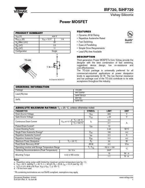
Power MOSFETIRF720, SiHF720Vishay SiliconixFEATURES•Dynamic dV/dt Rating •Repetitive Avalanche Rated •Fast Switching •Ease of Paralleling •Simple Drive Requirements •Lead (Pb)-free AvailableDESCRIPTIONThird generation Power MOSFETs from Vishay provide the designer with the best combination of fast switching,ruggedized device design, low on-resistance and cost-effectiveness.The TO-220 package is universally preferred for all commercial-industrial applications at power dissipation levels to approximately 50 W. The low thermal resistance and low package cost of the TO-220 contribute to its wide acceptance throughout the industry.Notesa.Repetitive rating; pulse width limited by maximum junction temperature (see fig. 11).b.V DD = 50 V, starting T J = 25 °C, L = 30 mH, R G = 25 Ω, I AS = 3.3 A (see fig. 12).c.I SD ≤ 3.3 A, dI/dt ≤ 65 A/µs, V DD ≤ V DS , T J ≤ 150 °C.d. 1.6 mm from case.PRODUCT SUMMARYV DS (V)400 VR DS(on) (Ω)V GS = 10 V1.8Q g (Max.) (nC)20Q gs (nC) 3.3Q gd (nC)11ConfigurationSingleTO-220GD S ORDERING INFORMATIONPackage TO-220Lead (Pb)-free IRF720PbF SiHF720-E3 SnPbIRF720SiHF720ABSOLUTE MAXIMUM RATINGS T C = 25 °C, unless otherwise notedARAMETER SYMBOL LIMIT UNIT Drain-Source Voltage V DS400VGate-Source Voltage V GS ± 20VContinuous Drain Current V GS at 10 VT C = 25 °C I D3.3A T C = 100 °C2.1Pulsed Drain Current a I DM 13Linear Derating Factor0.40W/°C Single Pulse Avalanche Energy b E AS 190mJ Repetitive Avalanche Current a I AR 3.3 A Repetitive Avalanche Energy a E AR 5.0mJ Maximum Power Dissipation T C = 25 °CP D 50WPeak Diode Recovery dV/dt cdV/dt 4.0V/ns Operating Junction and Storage Temperature Range T J , T stg- 55 to + 150°C Soldering Recommendations (Peak Temperature)for 10 s 300d Mounting Torque6-32 or M3 screw10 lbf · in 1.1N · m * Pb containing terminations are not RoHS compliant, exemptions may applyIRF720, SiHF720Vishay SiliconixNotesa.Repetitive rating; pulse width limited by maximum junction temperature (see fig. 11).b.Pulse width ≤ 300 µs; duty cycle ≤ 2 %.THERMAL RESISTANCE RATINGSARAMETER SYMBOL TY.MAX.UNITMaximum Junction-to-Ambient R thJA -62°C/W Case-to-Sink, Flat, Greased Surface R thCS 0.50-Maximum Junction-to-Case (Drain)R thJC- 2.5IRF720, SiHF720Vishay SiliconixCIRF720, SiHF720 Vishay SiliconixIRF720, SiHF720Vishay SiliconixFig. 10a - Switching Time Test CircuitFig. 10b - Switching Time WaveformsFig. 11 - Maximum Effective Transient Thermal Impedance, Junction-to-CaseFig. 12a - Unclamped Inductive Test CircuitFig. 12b - Unclamped Inductive WaveformsIRF720, SiHF720Vishay SiliconixFig. 13a - Basic Gate Charge WaveformFig. 13b - Gate Charge Test CircuitIRF720, SiHF720Vishay Siliconix Array Fig. 14 - For N-ChannelVishay Siliconix maintains worldwide manufacturing capability. Products may be manufactured at one of several qualified locations. Reliability data for Silicon Technology and Package Reliability represent a composite of all qualified locations. For related documents such as package/tape drawings, part marking, andreliability data, see /ppg?91043.Disclaimer Legal Disclaimer NoticeVishayAll product specifications and data are subject to change without notice.Vishay Intertechnology, Inc., its affiliates, agents, and employees, and all persons acting on its or their behalf (collectively, “Vishay”), disclaim any and all liability for any errors, inaccuracies or incompleteness contained herein or in any other disclosure relating to any product.Vishay disclaims any and all liability arising out of the use or application of any product described herein or of any information provided herein to the maximum extent permitted by law. The product specifications do not expand or otherwise modify Vishay’s terms and conditions of purchase, including but not limited to the warranty expressed therein, which apply to these products.No license, express or implied, by estoppel or otherwise, to any intellectual property rights is granted by this document or by any conduct of Vishay.The products shown herein are not designed for use in medical, life-saving, or life-sustaining applications unless otherwise expressly indicated. Customers using or selling Vishay products not expressly indicated for use in such applications do so entirely at their own risk and agree to fully indemnify Vishay for any damages arising or resulting from such use or sale. Please contact authorized Vishay personnel to obtain written terms and conditions regarding products designed for such applications.Product names and markings noted herein may be trademarks of their respective owners.元器件交易网。
IRF8721TRPBF;IRF8721PBF;中文规格书,Datasheet资料
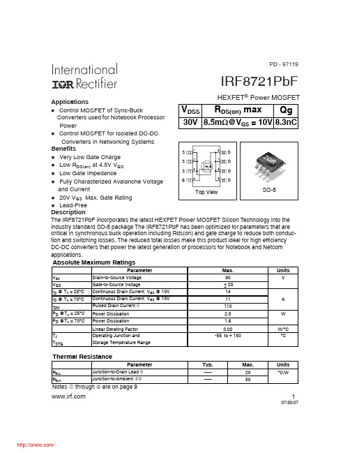
107/30/07IRF8721PbFHEXFET ®Power MOSFETBenefitsl Very Low Gate Charge l Low R DS(on) at 4.5V V GS l Low Gate Impedancel Fully Characterized Avalanche Voltage and Currentl 20V V GS Max. Gate Rating l Lead-Free Applicationsl Control MOSFET of Sync-BuckConverters used for Notebook Processor Powerl Control MOSFET for Isolated DC-DC Converters in Networking Systems SO-8PD - 97119DescriptionThe IRF8721PbF incorporates the latest HEXFET Power MOSFET Silicon Technology into the industry standard SO-8 package The IRF8721PbF has been optimized for parameters that are critical in synchronous buck operation including Rds(on) and gate charge to reduce both conduc-tion and switching losses. The reduced total losses make this product ideal for high efficiency DC-DC converters that power the latest generation of processors for Notebook and Netcom applications.IRF8721PbFStatic @ T = 25°C (unless otherwise specified)IRF8721PbF 3Fig 4. Normalized On-ResistanceVs. TemperatureFig 2. Typical Output CharacteristicsFig 1. Typical Output Characteristics Fig 3. Typical Transfer CharacteristicsV DS , Drain-to-Source Voltage (V)T J , Junction Temperature (°C)R D S (o n ) , D r a i n -t o -S o u r c e O n R e s i s t a n c e(N o r m a l i z e d )V GS , Gate-to-Source Voltage (V)V DS , Drain-to-Source Voltage (V)IRF8721PbFFig 8. Maximum Safe Operating AreaFig 6. Typical Gate Charge Vs.Gate-to-Source VoltageFig 5. Typical Capacitance Vs.Drain-to-Source VoltageFig 7. Typical Source-Drain DiodeForward Voltage110100V DS , Drain-to-Source Voltage (V)100100010000C , C a p a c i t a n c e (p F )0.11101001000I S D , R e v e r s e D r a i n C u r r e n t (A )0.1110100V DS , Drain-to-Source Voltage (V)0.11101001000I D , D r a i n -t o -S o u r c e C u r r e n t (A)510152025Q g , Total Gate Charge (nC)0481216V G S , G a t e -t o -S o u r c e V o l t a g e (V )IRF8721PbF 5Fig 11. Maximum Effective Transient Thermal Impedance, Junction-to-AmbientFig 9. Maximum Drain Current Vs.Case TemperatureFig 10. Threshold Voltage Vs. Temperature255075100125150T A , Ambient Temperature (°C)0481216I D , D r a i n C u r r e n t (A)T J , Temperature ( °C )V G S (t h ) G a t e t h r e s h o l d V o l t a g e (V )t 1, Rectangular Pulse Duration (sec)T h e r m a l R e s p o n s e ( Z t h J A )Fig 13. Maximum Avalanche Energyvs. Drain CurrentFig 12. On-Resistance vs. Gate VoltageFig 15b. Switching Time WaveformsFig 14b. Unclamped Inductive WaveformsFig 14a. Unclamped Inductive Test CircuitI ASFig 15a. Switching Time Test Circuit6810121416R D S (o n ), D r a i n -t o-S o u r c e O n R e s i s t a n c e (m Ω)V DDStarting T J , Junction Temperature (°C)V V d(on)rd(off)fV DDIRF8721PbF7DSCurrent Sampling ResistorsFig 16a. Gate Charge Test CircuitFig 16b. Gate Charge WaveformFig 17. Peak Diode Recovery dv/dt Test Circuit for N-ChannelHEXFET ® Power MOSFETs* V GS = 5V for Logic Level DevicesIdQgs1Qgs2Qgd QgodrIRF8721PbFSO-8 Package OutlineDimensions are shown in milimeters (inches)IRF8721PbF 9Notes:Repetitive rating; pulse width limited by max. junction temperature. Starting T J = 25°C, L = 1.09mH, R G = 25Ω, I AS = 11A. Pulse width ≤ 400μs; duty cycle ≤ 2%.When mounted on 1 inch square copper board. R θ is measured at T J of approximately 90°C.Data and specifications subject to change without notice.This product has been designed and qualified for the Consumer market.Qualification Standards can be found on IR’s Web site.IR WORLD HEADQUARTERS: 233 Kansas St., El Segundo, California 90245, USA Tel: (310) 252-7105TAC Fax: (310) 252-7903Visit us at for sales contact information .07/2007Note: For the most current drawing please refer to IR website at /package/330.00(12.992) MAX.14.40 ( .566 )12.40 ( .488 )NOTES :1. CONTROLLING DIMENSION : MILLIMETER.2. OUTLINE CONFORMS TO EIA-481 & EIA-541.FEED DIRECTIONTERMINAL NUMBER 112.3 ( .484 )11.7 ( .461 )8.1 ( .318 )7.9 ( .312 )NOTES:1. CONTROLLING DIMENSION : MILLIMETER.2. ALL DIMENSIONS ARE SHOWN IN MILLIMETERS(INCHES).3. OUTLINE CONFORMS TO EIA-481 & EIA-541.SO-8 Tape and ReelDimensions are shown in milimeters (inches)分销商库存信息:IRIRF8721TRPBF IRF8721PBF。
SY7201-DATASHEET
Features
• • • • • • • • Input voltage range 2.5V to 30V Switch current limit 2A Drives LED strings up to 30V 1MHz fixed frequency minimizes the external components Internal softstart limits the inrush current Open LED overvoltage protection RoHS Compliant and Halogen Free Compact package: SOT23-6 pin
Recommended Operating Conditions (Note 3) IN, ------------------------------------------------------------------------------------------------------------------- 2.5V to 30V LX, OVP ----------------------------------------------------------------------------------------------------------- 2.5V to 30V All other pins ------------------------------------------------------------------------------------------------------ 0 to 3.6V Junction Temperature Range ------------------------------------------------------------------------------------ -40°C to 125°C Ambient Temperature Range ----------------------------------------------------------------------------------- -40°C to HDN VREF IFB RDS(ON) ILIM VENH VENL VUVLO VHYS FOSC TSD THYST VOCL
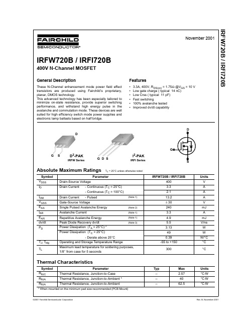
IRFW720中文资料
(Note 4)(Note 4, 5)(Note 4, 5) (Note 4)Notes:1. Repetitive Rating : Pulse width limited by maximum junction temperature2. L = 39mH, I AS =3.3A, V DD = 50V, R G = 25 Ω, Starting T J = 25°C 3. I SD ≤ 3.3A, di/dt ≤ 300A/µs, V DD ≤ BV DSS, Starting T J = 25°C4. Pulse Test : Pulse width ≤300µs, Duty cycle ≤2%5. Essentially independent of operating temperatureI GSSRGate-Body Leakage Current, ReverseV GS = -30 V, V DS = 0 V-----100nAOn CharacteristicsV GS(th)Gate Threshold Voltage V DS = V GS , I D = 250 µA 2.0-- 4.0V R DS(on)Static Drain-Source On-ResistanceV GS = 10 V, I D = 1.65 A -- 1.4 1.75Ωg FSForward TransconductanceV DS = 40 V, I D = 1.65 A--2.8--SDynamic CharacteristicsC iss Input Capacitance V DS = 25 V, V GS = 0 V, f = 1.0 MHz--460600pF C oss Output Capacitance--5572pF C rssReverse Transfer Capacitance--1115pFSwitching Characteristicst d(on)Turn-On Delay Time V DD = 200 V, I D = 3.3 A,R G = 25 Ω--1030ns t r Turn-On Rise Time --3580ns t d(off)Turn-Off Delay Time --3580ns t f Turn-Off Fall Time --3580ns Q g Total Gate Charge V DS = 320 V, I D = 3.3 A,V GS = 10 V--1418nC Q gs Gate-Source Charge -- 2.7--nC Q gdGate-Drain Charge--5.6--nCDrain-Source Diode Characteristics and Maximum RatingsI S Maximum Continuous Drain-Source Diode Forward Current ---- 3.3A I SM Maximum Pulsed Drain-Source Diode Forward Current----13.2A V SD Drain-Source Diode Forward Voltage V GS = 0 V, I S = 3.3 A ---- 1.5V t rr Reverse Recovery Time V GS = 0 V, I S = 3.3 A,dI F / dt = 100 A/µs--220--ns Q rrReverse Recovery Charge-- 1.36--µCDISCLAIMERFAIRCHILD SEMICONDUCTOR RESERVES THE RIGHT TO MAKE CHANGES WITHOUT FURTHER NOTICE TO ANY PRODUCTS HEREIN TO IMPROVE RELIABILITY, FUNCTION OR DESIGN. FAIRCHILD DOES NOT ASSUME ANY LIABILITY ARISING OUT OF THE APPLICATION OR USE OF ANY PRODUCT OR CIRCUIT DESCRIBED HEREIN;NEITHER DOES IT CONVEY ANY LICENSE UNDER ITS PATENT RIGHTS, NOR THE RIGHTS OF OTHERS.LIFE SUPPORT POLICYFAIRCHILD’S PRODUCTS ARE NOT AUTHORIZED FOR USE AS CRITICAL COMPONENTS IN LIFE SUPPORT DEVICES OR SYSTEMS WITHOUT THE EXPRESS WRITTEN APPROVAL OF FAIRCHILD SEMICONDUCTOR CORPORATION.As used herein:1. Life support devices or systems are devices or systems which, (a) are intended for surgical implant into the body,or (b) support or sustain life, or (c) whose failure to perform when properly used in accordance with instructions for use provided in the labeling, can be reasonably expected to result in significant injury to the user.2. A critical component is any component of a life support device or system whose failure to perform can be reasonably expected to cause the failure of the life support device or system, or to affect its safety or effectiveness.PRODUCT STATUS DEFINITIONS Definition of TermsDatasheet Identification Product Status DefinitionAdvance InformationFormative or In Design This datasheet contains the design specifications for product development. Specifications may change in any manner without notice.PreliminaryFirst ProductionThis datasheet contains preliminary data, andsupplementary data will be published at a later date.Fairchild Semiconductor reserves the right to make changes at any time without notice in order to improve design.No Identification Needed Full ProductionThis datasheet contains final specifications. Fairchild Semiconductor reserves the right to make changes at any time without notice in order to improve design.Obsolete Not In ProductionThis datasheet contains specifications on a product that has been discontinued by Fairchild semiconductor.The datasheet is printed for reference information only.TRADEMARKSThe following are registered and unregistered trademarks Fairchild Semiconductor owns or is authorized to use and is not intended to be an exhaustive list of all such trademarks.STAR*POWER is used under licenseACEx™Bottomless™CoolFET™CROSSVOLT ™DenseTrench™DOME™EcoSPARK™E 2CMOS™EnSigna™FACT™FACT Quiet Series™FAST ®FASTr™FRFET™GlobalOptoisolator™GTO™HiSeC™ISOPLANAR™LittleFET™MicroFET™MicroPak™MICROWIRE™OPTOLOGIC™OPTOPLANAR™PACMAN™POP™Power247™PowerTrench ®QFET™QS™QT Optoelectronics™Quiet Series™SLIENT SWITCHER ®SMART START™STAR*POWER™Stealth™SuperSOT™-3SuperSOT™-6SuperSOT™-8SyncFET™TruTranslation™TinyLogic™UHC™UltraFET ®VCX™。
IRF7201TR中文资料
Top View
The SO-8 has been modified through a customized leadframe for enhanced thermal characteristics and multiple-die capability making it ideal in a variety of power applications. With these improvements, multiple devices can be used in an application with dramatically reduced board space. The package is designed for vapor phase, infra red, or wave soldering techniques. Power dissipation of greater than 0.8W is possible in a typical PCB mount application.
When mounted on 1 inch square copper board, t<10 sec
2
元器件交易网
ID , Drain-to-Source Current (A)
IRF7201
100
VGS
TOP
15V
10V
7.0V
5.5V
4.5V
0.1 0.4
VGS = 0V A
0.6
0.8
1.0
1.2
VSD , Source-to-Drain Voltage (V)
Fig 4. Typical Source-Drain Diode Forward Voltage
IRF820数据手册
mm TYP. MAX. 4.60 1.32 2.72 1.27 0.70 0.88 1.70 1.70 5.15 2.7 10.40 0.019 0.024 0.044 0.044 0.194 0.094 0.393 MIN. 0.173 0.048 0.094 4.40 1.23 2.40
inch TYP. MAX. 0.181 0.051 0.107 0.050 0.027 0.034 0.067 0.067 0.203 0.106 0.409 0.645 0.551 0.116 0.620 0.260 0.154 0.151
August 1998
1/8
IRF820
THERMAL DATA
R t hj-ca se
Rthj -amb
R thc- si nk Tl
Thermal Resistance Junction-case Max Thermal Resistance Junction-ambient Max Thermal Resistance Case-sink Typ Maximum Lead Temperature For Soldering Purpose
1.56 62.5 0.5 300
C/W oC/W o C/W o C
o
AVALANCHE CHARACTERISTICS
Symb ol I AR E AS Parameter Avalanche Current, Repetitive or Not-Repetitive (pulse width limited by Tj max) Single Pulse Avalanche Energy (starting Tj = 25 o C, I D = IAR , VDD = 50 V) Max Valu e 2.5 210 Unit A mJ
720HE产品说明书20140311

产品说明书中孚P C I-E网络安全隔离卡————————用户使用说明书山东中孚信息产业股份有限公司1产品说明书目录第一部分USB通讯串口数据线切换型(HDP-III K720HE) (3)一、产品简介 (3)二、隔离卡示意图 (4)三、安装前注意事项 (5)四、安装步骤 ................................................................... .5 第二部分管理软件的安装使用 (8)第三部分产品的卸载 (20)第四部分技术服务 ............................................................. .212产品说明书第一部分 USB通讯串口数据线切换型(HDP-III K720HE)一、产品简介USB通讯串口数据线切换型HDP-III K720HE是插在主板PCI-E槽上的升级整合型PCI-E接口隔离卡。
通过系统下的管理软件实现实时切换、重启切换、关机选网功能,适用于两块硬盘都是串口硬盘,支持双布线的百兆网络环境。
HDP-III K720HE百兆隔离卡集成了四套程序,通过x1和x2跳线帽来控制:出厂默认:x1跳线帽在下面,x2跳线帽在上面;x1跳线帽在下面,x2跳线帽在上面:如果不出界面,需要进BIOS,设置USB CDRM或CD/DVD为第一引导项(有些机器需要将ZFEC USB CDRM或USB:ZFEC USBCARD设为第一引导项)。
x1跳线帽在上面,x2跳线帽在上面:没有选网界面。
x1跳线帽在上面,x2跳线帽在下面:没有选网界面。
x1跳线帽在下面,x2跳线帽在下面:必须先在外网硬盘装选网界面:从光盘引导,选择"USB系列隔离卡界面安装",输入命令:Install。
x1跳线帽在下面,x2跳线帽在下面:安装管理软件之前,请务必确认以下几点:1.必须用外加硬盘(非机器本身自带硬盘)做外网!3产品说明书2.必须先用光盘在外网硬盘上安装选网界面!3.必须确认外网硬盘无隐藏分区!以上条件如不符合,会造成数据安全问题,请勿安装本管理软件,否则后果自负!建议:不要随意更改跳线帽位置,遇问题可联系我客服人员!二、隔离卡示意图USB通讯串口数据线切换型(HDP-III K720HE)4产品说明书三、安装前注意事项1、首先请准备两块SATA接口的硬盘,对硬盘进行分区,并安装好各自的操作系统和应用软件。
IRS2101STRPBF中文资料
2
元器件交易网
IRS2101(S)PbF
Dynamic Electrical Characteristics
VBIAS (VCC, VBS) = 15 V, CL = 1000 pF and TA = 25 °C unless otherwise specified.
50 1.0 0.625 125 200 150 150 300
Units
V
V/ns W
°C/W °C
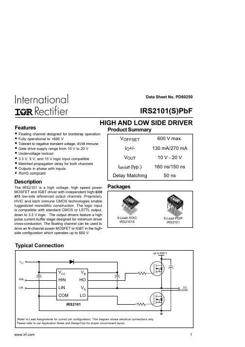
Recommended Operating Conditions
The input/output logic timing diagram is shown in Fig. 1. For proper operation the device should be used within the recommended conditions. The VS offset rating is tested with all supplies biased at a 15 V differential.
Package power dissipation @ TA ≤ +25 °C
Thermal resistance, junction to ambient
Junction temperature Storage temperature Lead temperature (soldering, 10 seconds)
V
— 0.05 0.2
IO = 2 mA
— 0.02 0.1
—
—
50
VB = VS = 600 V
—
30 55
— 150 270 µA
VIN = 0 V or 5 V
MT7201C中文
MT7201C+ 3.55 版
美芯晟科技有限公司
第7页
MT7201C+
1A 内置功率管 LED 恒流驱动器
Voltage of ADJ Pin (V)
MT7201C+ 3.55 版
美芯晟科技有限公司
第6页
MT7201C+
1A 内置功率管 LED 恒流驱动器
应用说明
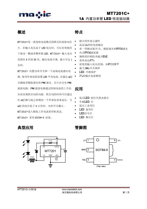
通过外部电流采样电阻 RS 设定 LED 平均电 流 LED 的平均电流由连接在 VIN 和 ISENSE 两端 的电阻 RS 决定: IOUTnom = 0.1/RS [for RS>0.1] 下表给出了输出电流和 RS 关系的一些典型例子: RS(Ω) 输出平均电流 (mA) 0.1 1000 0.13 760 0.15 667 以上说明成立的前提是 ADJ 脚悬空。 注意: 在保持开关电流低于指定的最大值时, 允 许感应电阻最小值为 Rs=0.1 Ω。 如果 ADJ 端是通过外部电压,Rs 值也可以是其 他值。 通过直流电压实现模拟调光 ADJ 端可以外加一个直流电压(VADJ), 来调小 LED 输出电流,最大 LED 输出电流由 RS 设定,如图 所示:
MT7201C+ 3.55 版
美芯晟科技有限公司
第3页
MT7201C+
1A 内置功率管 LED 恒流驱动器
内部框图
典型工作曲线
(如无特别说明,电感 L=47uH)
1LED Efficiency vs. Input Voltage
90% 85%
x
380
Current vs. Vin (1LED, 300mA)
Vin (V)
MT7201C+ 3.55 版
72045中文资料
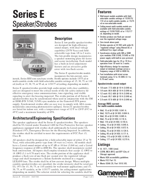
Series E CS-2243 10/17/03Page 1 of 2DescriptionSeries E low-profile speaker/strobesare designed for high-efficiencysound output, with dual voltagecapability (25/70 V RMS ) and field-selectable taps from 1/8 to 2 watts.The low-profile design incorporatesa speaker mounting plate for faster and easier installation. Each modelhas a built-in level adjustmentfeature and an attractive grillecover with two flush screws.The Series E speaker/strobe modelsincorporate the low-current, zero-inrush, Series RSS non-sync/sync strobe. Strobe options include 15/75 cd ormulti-candela strobe with field-selectable candela settings of: 15, 30, 75, or 110cd (wall); or 15, 30, 75, or 95 cd, or 115/177 cd (ceiling, depending on model).Series E speaker/strobes provide high audio output with clear audibility,and are designed to meet the critical needs of the life safety industry foreffective emergency voice communications, tone signaling, and visiblesignaling to alert the hearing impaired. The strobe portion of all Series Espeaker/strobes may be synchronized when used in conjunction with the SMor DSM (P/N 51548, 51549) sync modules or the Gamewell FF8 powersupply. Synchronized strobes offer an easy way to comply with ADA recom-mendations concerning photosensitive epilepsy. Series E speaker/strobesare listed for indoor use, with a temperature range of 32°F to 120°F (0°C to49°C) and a maximum humidity of 85%.Architectural/Engineering SpecificationsThe speaker appliances shall be Series E speaker/strobes. The speakersshall be UL Listed under Standard 1480 for Fire Protective Service; speakerappliances equipped with strobes shall additionally be Listed under ULStandard 1971, Emergency Devices for the Hearing Impaired. In addition,the strobes shall be certified to meet the requirements of FCC Part 15,Class B.All speakers shall be designed for a field-selectable input of either 25 or 70V RMS , with selectable power taps from 1/8 watt to 2 watts. All models shallhave a Listed sound output of up to 87 dB at 10 feet (3.048 m), and a Listedfrequency response of 400 to 4000 Hz. The speaker shall incorporate sealedback construction. All inputs shall employ terminals that accept 12 AWG to18 AWG (3.1 to 0.78 mm²) wire. The strobe portion of the appliance shallproduce a flash rate of one flash per second over the regulated voltagerange and shall incorporate a Xenon flashtube enclosed in a ruggedLEXAN® lens. The strobe shall be of low-current design. Where multiple-candela speaker/strobes are specified, the strobe intensity shall be rated perUL 1971 for 15, 30, 75, or 110 candela for wall-mount applications; and 15,30, 75, or 95 candela, or for 115/177 candela, for ceiling-mount applications(depending on model). The selector switch for selecting the candela shall beFeatures •Wall-mount models available with field-selectable candela settings of 15/30/75/110 cd on multi-candela models, or 15/75cd on non-selectable model.•Ceiling-mount multi-candela models are available with field-selectable candela settings of 15/30/75/95 cd or 115/177cd, depending on model.•Strobes produce one flash per second over the regulated voltage range.•Zero inrush above peak.•Strobes operate at 24 VDC with wide UL “regulated voltage” using filtered DC or unfiltered V RMS input voltage.•Synchronize strobes with SM or DSM sync modules (P/N 51548, 51549) or FF8power supply with built-in sync protocol.•Field-selectable taps for 25 or 70 V RMS operation from 1/8 watt to 2 watts.•High-efficiency design for maximum output at minimum wattage across a frequency range of 400 to 4000 Hz.•Fast installation with in/out screw terminals using 12 to 18 AWG (3.1 to 0.78 mm²) wires.Speaker/strobe sound output •1/8 watt: 77.5 dBA @ 10 ft (3.048 m).•1/4 watt: 80.4 dBA @ 10 ft (3.048 m).•1/2 watt: 83.2 dBA @ 10 ft (3.048 m).•1.0 watt: 85.7 dBA @ 10 ft (3.048 m).•2.0 watt: 87.8 dBA @ 10 ft (3.048 m).Average RMS current for multi-candela models •Wall, 15 cd @ 24 VDC: 0.041 A.•Wall, 15/75 cd @ 24 VDC: 0.064 A.•Wall, 30 cd @ 24 VDC: 0.065 A.•Wall, 75 cd @ 24 VDC: 0.116 A.•Wall, 110 cd @ 24 VDC: 0.155 A.•Ceiling, 15 cd @ 24 VDC: 0.045 A.•Ceiling, 30 cd @ 24 VDC: 0.072 A.•Ceiling, 75 cd @ 24 VDC: 0.128 A.•Ceiling, 95 cd @ 24 VDC: 0.171 A.•Ceiling, 115 cd @ 24 VDC: 0.195 A.•Ceiling, 177 cd @ 24 VDC: 0.270 A.Listings •UL 1971, 1480 Listed.•CSFM, MEA (NYC) and BFP (City of Chicago) approved.•Meets ADA accessibility guidelines.•Meets FCC Part 15.•Meets OSHA 29, Part 1910.165.Series ESpeaker/Strobes5741ss70.jpg5741ss90.jpgSeries E CS-2243 10/17/03Page 2 of 2 AC opyright ©2003 Specifications and wiring information are provided for information only and are believed to be accurate. Gamewell assumes no responsibility for their use.Data and design are subject to change without notice. Installation and wiring instructions shipped with the product shall always be used for actual installation.For more information, contact Gamewell.tamper resistant. The 15/75 candela wall strobe shall be specified when 15 candela UL 1971 Listing with 75 candela intensity on-axis is required (e.g., ADA compliance). When synchronization is required, the strobe portion of the appliance shall be compatible with SM and DSM (P/N 71548, 71549) sync modules and the Gamewell FF8 power supply with built-in sync protocols. The strobes shall not drift out of synchronization at any time during operation.If the sync module or power supply fails to operate (i.e., contacts remain closed), the strobes shall revert to a non-synchronized default flash rate of one flash per second.The speaker/strobe appliances shall be designed for indoor surface- or flush-mounting. The speaker/strobes shall incorporate a speaker mounting plate with a grille cover, which is secured with two screws for a level, aesthetic finish. Speaker/strobes shall mount to standard electrical hardware requiring no additional trimplate or adapter.Speaker/strobes shall be finished in a textured red or white color. All speaker/strobe appliances shall be backward compatible.Ordering InformationAll 24 V models below feature field-selectable taps for 25 or 70 V RMS operation, from 1/8 watt to 2 watts.72045Wall-mount multi-candela (15, 30, 75, 110) speaker/strobe, 24 VDC, square, red (E70-24MCW-FR ).72046Wall-mount multi-candela (15, 30, 75, 110) speaker/strobe, 24 VDC, square, white (E70-24MCW-FW ).7174515/75-candela speaker/strobe, wall-mount, 24 VDC, 0.064 A, square, red (E70-241575W-FR ).72285Ceiling-mount multi-candela (15, 30, 75, 95) speaker/strobe, 24 VDC, round, white (E90-24MCC-FW ).72286Ceiling-mount multi-candela (115, 177) speaker/strobe, 24 VDC, round, white (E90-24MCCH-FW ).Sync modules, power supply71548SM sync module, single-circuit Class B, rated for 3.0 A @ 24 VDC (SM-12/24-R ).71549DSM sync module, single-circuit Class A or multiple-circuit Class B, rated for 3.0 A per circuit. The maximum number of interconnected modules is 20 (DSM-12/24-R ).FF8FireForce 8, NAC expander/power supply. 12/24 VDC, 8.0 A, 4 NACs, built-in sync protocols.See data sheet CS-2282.Mounting accessories for Series E speaker/strobes70418Surface-mount backbox, 5.5" (13.970 cm) x 5.563" (14.129 cm) x 3.563" (9.049 cm), red (SBB-R ).71317Extender, molded, 5.25" (13.335 cm) square 0.781" (1.984 cm) deep, red (ISP-R ).71318Retrofit plate, 8.0" (20.320 cm) x 5.875" (14.923 cm) x 0.406" (1.032 cm) deep, red (RP-R ).68292Semi-flush plate, 6.0" (15.240 cm) square x 0.313" (0.794 cm) deep, red (SFP-R ).。
Arista Cognitive Campus 720XP 系列交换机说明书

概述Arista Cognitive Campus 720XP 系列交换机在 Arista Cognitive Campus Services 的管理和监控下,为所有园区⽤户⼯作负载提供了连接性和功能。
该平台套件为⽤户桌⾯,PoE 设备和 IoT 设备提供了多种连接选项。
托管的 802.3af/at/bt 电源服务可为每个 RJ45 端⼝提供⾼达 60W 的功率,速度选项从 10Mbps 到 5Gbps 。
模块化 SFP+ 和 QSFP+ 上⾏链路⽀持从 1Gbps 到 100Gbps 的速度,从⽽提供⽹络设计的灵活性和可扩展性。
园区 PoE 10M/100G 交换机数据表产品亮点以太⽹供电加 25/100G 720XP-48ZC2•40 x mGig (100M - 2.5Gb) RJ45 @ 30W •8 x mGig (100M - 5Gb) RJ45 @ 60W •上⾏链路:4x 25G, 2x 100G720XP-24ZY4•16 x mGig (100M - 2.5Gb) RJ45 @ 30W •8x mGig (100M - 5Gb) RJ45 @ 60W •上⾏链路:4x 25G720XP-48Y6•48 x 10M-1GbE RJ45 @ 30W •上⾏链路:6x 25G720XP-24Y6•24x 10M-1GbE RJ45 @ 30W •上⾏链路:6x 25G分割和重叠•4096 802.1Q VLANs •IPv4/v6 VRFs•1670 万个 VXLAN ⽹络 •EVPN L2/3(类型 2/5)流量监控•硬件加速监控 •带内⽹络遥测 •sFlow 和 IPFIX•FlowTracker 可以清点设备并监控对话认知校园弹性•N+1 冗余电源/冷却 •主动/主动 MLAG 聚合 •动态上⾏链路负载均衡 •⽤于软件升级和 ⽆缝修补的 ISSUArista EOS•单⼀⼆进制映像•细粒度真正模块化⽹络操作系统 •状态化故障隔离 (SFC) •状态化故障修复 (SFR)•完全访问 Linux shell 和⼯具 •可扩展平台 - bash, python, C++ , GO, OpenConfig认知园区Arista EOS 中的认知管理平⾯ (CMP) 提供了丰富的控制和遥测 API ,⽤于简化和⾃动化校园基础架构的部署和维护,同时还提供对校园⽤户,应⽤和设备的实时监控。
映翰通IR720路由器规格书
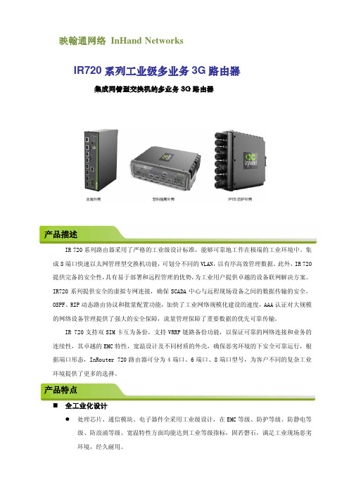
映翰通网络InHand NetworksIR720系列工业级多业务3G路由器集成网管型交换机的多业务3G路由器产品描述IR 720系列路由器采用了严格的工业级设计标准,能够可靠地工作在极端的工业环境中。
集成8端口快速以太网管理型交换机功能,可划分不同的VLAN,以有序高效管理数据。
此外,IR 720提供完备的安全性,具有易于部署和远程管理的优势,为工业用户提供卓越的设备联网解决方案。
IR720系列提供安全的虚拟专网连接,确保SCADA中心与远程现场设备之间的数据传输的安全,OSPF、RIP动态路由协议和批量配置功能,加快了工业网络规模化建设的速度,AAA认证对大规模的网络设备管理提供了强大的安全保障,流量管理保障了重要数据的优先可靠传输。
IR 720支持双SIM卡互为备份,支持VRRP链路备份功能,以保证可靠的网络连接和业务的连续性,其卓越的EMC特性,宽温设计及不同材质的外壳,确保恶劣环境的下安全可靠运行,根据端口形态,InRouter 720路由器可分为4端口、6端口、8端口型号,为客户不同的复杂工业环境提供了更多的选择。
产品特点⏹全工业化设计●处理芯片、通信模块、电子器件全采用工业级设计,在EMC等级、防护等级、防静电等级、防浪涌等级、宽温特性方面均能达到工业等级指标,固若磐石,满足工业现场恶劣环境,经久耐用。
●超强防护等级,金属外壳IP40、塑料隔离外壳IP40、防护外壳IP65。
●以太网口支持1.5KV 隔离耐压保护。
●宽温支持:-25℃~70℃。
●宽压支持DC9-48V。
⏹集成快速以太网管理型交换机功能●支持VLAN(VLAN-BASED、PORT-VLAN)、802.1Q、802.1x、●支持标准环网协议RSTP(802.1w)。
●支持端口安全,端口隔离、风暴抑制等安全功能有效的防止外来的恶意攻击。
●支持端口镜像,实时监控分析数据流,便于及时发现网络存在的问题。
●多达8个LAN口用于连接多个设备。
冰河科技 集团电话·交换机 用户手册说明书

目录一系统简介---------------------------------------------------------------------------------------41、系统配置说明---------------------------------------------------------------------------------42、功能特点---------------------------------------------------------------------------------------4二结构及技术指标----------------------------------------------------------------------------51、技术参数---------------------------------------------------------------------------------------52、安装注意事项---------------------------------------------------------------------------------63、警告---------------------------------------------------------------------------------------------64、电源及接地要求------------------------------------------------------------------------------65、系统安装步骤---------------------------------------------------------------------------------7三系统编程---------------------------------------------------------------------------------------71、恢复出厂状态---------------------------------------------------------------------------------82、编程密码修改---------------------------------------------------------------------------------83、闪断时间设置---------------------------------------------------------------------------------84、总机设置---------------------------------------------------------------------------------------95、分机互打来电显示设置---------------------------------------------------------------------96、普通外线出局号设置------------------------------------------------------------------------97、拨打总机号设置--------------------------------------------------------------------------108、*#键互换-------------------------------------------------------------------------------------109、分机闹钟设置-------------------------------------------------------------------------------1010、数码录音时间设置------------------------------------------------------------------------1011、数码录音------------------------------------------------------------------------------------1112、录音试听------------------------------------------------------------------------------------1113、音乐试听------------------------------------------------------------------------------------1214、设置自动值班等待语音接通时间------------------------------------------------------1215、无人接听转移时间------------------------------------------------------------------------1216、设置来电显示收号模式------------------------------------------------------------------1217、开通外线------------------------------------------------------------------------------------1318、日间(夜间)值班模式-------------------------------------------------------------------1319、设置外线日间(夜间)呼入振铃分机------------------------------------------------1320、外线呼入振铃延时------------------------------------------------------------------------1421、外线话务量使用分配------------------------------------------------------------------1422、外线自动值班无拨号处理------------------------------------------------------------1423、外线呼叫转移无人接听处理---------------------------------------------------------1424、开关内部呼叫代接功能---------------------------------------------------------------1525、开关内部通话转移功能---------------------------------------------------------------1526、排队振铃---------------------------------------------------------------------------------1527、分机出局方式设置---------------------------------------------------------------------1528、日间(夜间)呼出等级限制设置-----------------------------------------------------1529、呼出限时设置---------------------------------------------------------------------------1630、遇忙、无人接听转移设置-------------------------------------------------------------1631、呼叫无条件转移设置------------------------------------------------------------------1732、外线日间(夜间)使用权限设置-----------------------------------------------------1733、分机号码设置---------------------------------------------------------------------------1734、呼出限制字头设置---------------------------------------------------------------------1835、呼出特许字头设置---------------------------------------------------------------------1836、移动账号---------------------------------------------------------------------------------1937、计费延时时间设定---------------------------------------------------------------------1938、清除计费话单---------------------------------------------------------------------------19四使用方法-------------------------------------------------------------------------------------201、人工值班----------------------------------------------------------------------------------202、自动值班----------------------------------------------------------------------------------203、代接外(内)线-------------------------------------------------------------------------204、拨打外线----------------------------------------------------------------------------------205、预约外线----------------------------------------------------------------------------------206、选择外线----------------------------------------------------------------------------------207、外线转移----------------------------------------------------------------------------------218、拨打内线----------------------------------------------------------------------------------229、三方通话----------------------------------------------------------------------------------2210、外线保留--------------------------------------------------------------------------------2211、拨打总机--------------------------------------------------------------------------------2212、内线转移---------------------------------------------------------------------------------2213、分机查询功能---------------------------------------------------------------------------2214、系统日期时间查询功能--------------------------------------------------------------2315、系统版本查询功能---------------------------------------------------------------------2316、闹钟使用---------------------------------------------------------------------------------2417、移动账号使用方法--------------------------------------------------------------------------2418、监听--------------------------------------------------------------------------------------------2419、呼叫无条件转移----------------------------------------------------------------------------2420、遇忙、无人接听转移-----------------------------------------------------------------------2421、免打扰-----------------------------------------------------------------------------------------2522、群呼(紧急呼叫)--------------------------------------------------------------------------25附录一电话路由选择功能(可选)---------------------------------------------------------25附录二日夜值班功能设置--------------------------------------------------------------------28附录三IP加拨功能----------------------------------------------------------------------------29附录四外线联号功能--------------------------------------------------------------------------30附录五特色功能--------------------------------------------------------------------------------32附录六常见故障及排除-----------------------------------------------------------------------35附录七名称术语--------------------------------------------------------------------------------36附录八出厂默认--------------------------------------------------------------------------------37附录九系统功能编程指令--------------------------------------------------------------------38附录十操作使用代码--------------------------------------------------------------------------41产品质量保证说明--------------------------------------------------------------------------------42产品保修卡-----------------------------------------------------------------------------------------43一、系统简介1、系统配置说明:*本说明书适用于冰河TX6000集团电话(电话交换机)S、K、P等系列,说明书上所列出的功能必须该型号机型支持才可设置,具体请参照功能说明后面标注所支持的机型或产品的配置参数。
数字流量切换器PFMB7201 7501 7102 7202 PFMB7-TFQ04-A 二 产品部

Installation & Maintenance Manual Digital Flow SwitchPFMB7201/7501/7102/72022 Summary of Product partsWarningDo not disassemble, modify (including changing the printedcircuit board) or repair.An injury or failure can result.Do not operate the product outside of the specifications.Do not use for flammable or harmful fluids.Fire, malfunction, or damage to the product can result.Verify the specifications before use.Do not operate in an atmosphere containing flammable, explosiveor corrosive gas.Fire, explosion or corrosion can result.This product is not designed to be explosion proof.Do not use the product for flammable fluid.Fire or explosion can result.Only air and N2are applicable.Do not use the product in a place where static electricity is aproblem.Otherwise it can cause failure or malfunction of the system.If using the product in an interlocking circuit:•Provide a double interlocking system, for example a mechanicalsystem.•Check the product regularly for proper operation.Otherwise malfunction can result, causing an accident.The following instructions must be followed during maintenance:•Turn off the power supply.•Stop the air supply, exhaust the residual pressure and verify that theair is released before performing maintenance work.Otherwise an injury can result.CautionMounting•Never mount the product in a place where it will be used as a mechanicalsupport.•Mount the product so that the fluid flows in the direction indicated by thearrow on the side of the body.This manual contains essential information for the protection of usersand others from possible injury and/or equipment damage.•Read this manual before using the product, to ensure correct handling,and read the manuals of related apparatus before use.•Keep this manual in a safe place for future reference.•These instructions indicate the level of potential hazard by label of"Caution", "Warning" or "Danger", followed by important safetyinformation which must be carefully followed.•To ensure safety of personnel and equipment the safety instructions inthis manual and the product catalogue must be observed, along withother relevant safety practices.This product is class A equipment that is intended for use in an industrialenvironment.There may be potential difficulties in ensuring electromagneticcompatibility in other environments due to conducted as well as radiateddisturbances.Do not touch the terminals and connectors while the power is on.Otherwise electric shock, malfunction or damage to the product can result.After maintenance is complete, perform appropriate functionalinspections and leak tests.Stop operation if the equipment does not function properly or there is aleakage of fluid.When leakage occurs from parts other than the piping, the product mightbe faulty.Disconnect the power supply and stop the fluid supply.Do not apply fluid under leaking conditions.Safety cannot be assured in the case of unexpected malfunction.∗1: A protective tape is affixed to the display. Please remove it before use.∗2: The table lists the parts when a flow adjusting valve is included.BodyPanel mounting (Only PFMB7201)•Refer to the diagram and table below for mounting details.•Refer to the operation manual on the SMC website(URL )for panel thickness and panel cut-outdimensions.NOTEThe direct current power supply used should be UL approved as follows.Circuit (class 2) of maximum 30 Vrms (42.4 V peak) or less, with UL1310class 2 power supply unit or UL1585 class 2 transformer.The product is a UL approved product only if it has a mark on thebody.Bracket mounting (PFMB7501/7102/7202 shown below)•Refer to the diagram and table below for mounting details.•Refer to the operation manual on the SMC website(URL )for bracket thickness and mounting holedimensions.2Direct mounting•Refer to the diagram and table below for mounting details.•Refer to the operation manual on the SMC website(URL )for mounting hole sizes.PFMB7201PFMB7501/7102/7202∗3: When the reversed display is used, the function of the and buttons isreversed.DisplayPFMB7201PFMB7501/7102/7202DIN rail mounting (Only PFMB7201)•Refer to the diagram and table below for mounting details.Piping•Never mount the product upside down.•The straight piping length shall be 8 cm or longer.Otherwise, if a straight section of piping is not installed, the accuracyvaries by approximately ±2%F.S.•Avoid sudden changes in the piping size on the IN side of the product.•Do not release the OUT side piping port of the product directly to theatmosphere without the piping connected. If the product is used withthe piping port released to atmosphere, the accuracy may vary.Piping for the One-touch fitting•Accuracy can vary approximately±2% when tubing other than therecommended tubing is used.•Insert the tube all the way into thefitting so that it cannot be pulled out.•Insertion with excessive force cancause damage.•Ensure there is no leakage afterpiping.•Use the product within the specifiedRefer to the operation manual on the SMC website(URL ) for more information about safetyinstructions.3 Mounting and InstallationPiping for the metal attachment•Tighten to the specified torque. Refer to the table below for the required torque values.•Use a suitable spanner for the appropriate torque. Do not use a spanner 40 cm or longer.•If the tightening torque is exceeded, the product can be broken.If the tightening torque is insufficient, the fitting may become loose.•Avoid any sealing tape getting inside the flow path.•Ensure there is no leakage after piping.•When mounting the fitting, a spanner should be used on the metal part (attachment) of the fitting only.Holding other parts of the product with a spanner may damage the product.Specifically, make sure that the spanner does not damage the connector.3 step setting modeIn this mode, only the set values can be input, in just 3 steps.Use this mode if the product is to be used straight away, after changing onlythe set values.Default settingsWhen the flow exceeds the set value [P_1], the switch will be turned ON.When the flow falls below the set value by the amount of hysteresis [H_1]or more, the switch will turn OFF.If the operation shown in the diagram below is acceptable, then keepthese settings.Refer to the function selection mode to change the hysteresis.For more detailed settings, set each function in function selection mode.Operation(The example below is the explanation for PFMB7201(1 output type) when reverse function is not used.)Press the S button once in measurement mode.[P_1] or [n_1] and [the current set value] are displayed in turn.∗: For models with switch outputs for both OUT1 and OUT2, [P_2] or [n_2] will bedisplayed too.Set as above.∗: If a mode other than Hysteresis Mode is selected, refer to the operation manual fromSMC website (URL ) or contact SMC.∗: Note that the set value and hysteresis are limited by each other.∗: For more detailed settings, set each function in function selection mode.button to change the set value.button is to decrease the setPress the buttonkeepincreasing the set value.Press the buttonkeepdecreasing the set value.Press the S button to complete the setting.Return to measurement mode.23Function selection modeIn this mode, each function setting can be changed separately.In measurement mode, press the S button for 2 seconds or longer tobutton to select the function to be changed.WiringConnection•Connections should only be made with the power supply turned off.•Use a separate route for the product wiring and any power or highvoltage wiring. Otherwise, malfunction may result due to noise.•Ensure that the FG terminal is connected to ground when using acommercially available switch-mode power supply. When a switch-mode power supply is connected to the product, switching noise willbe superimposed and the product specification can no longer be met.This can be prevented by inserting a noise filter, such as a line noisefilter and ferrite core, between the switch-mode power supply and theproduct or by using a series power supply instead of a switch-modepower supply.Connecting/Disconnecting•When mounting the connector, insert itstraight into the socket, holding the leverand connector body, and push theconnector until the lever hooks into thehousing, and locks.•When removing the connector, pressdown the lever to release the hook fromthe housing and pull the connectorstraight out.Power is suppliedPress the S buttononce.Press the S button for2 seconds or longer.∗: The outputs will continue to operate during setting.∗: If a button operation is not performed for 30 seconds during the setting, the displaywill flash.(This is to prevent the setting from remaining incomplete if, for instance, an operatorwere to leave during setting)∗: 3 step setting mode and Function selection mode are reflected on each other.mode are used during fluctuating flow conditions. In this case, maintain an intervalbetween the set values and start using after confirming stable operation.Select the operation required from the table below.For example . . .•Turn the switch output ON when the flow exceeds the set value.•Turn the switch output ON when the flow falls below the set value.•Turn the switch output ON when the flow is more, or less, than aspecific flow range.Switch output operation list5 Flow Setting (set value only) of OUT1 •OUT216 Function SettingPress the S button for 2 seconds or longer in function selectionmode to return to measurement mode.Refer to the specific product precautions in the operation manual on theSMC website (URL ) for more informationabout installation.1ACBIn measurement mode, press the S button for 2 seconds or longer todisplay [F 0].or button to display [F99]. Press the S button.orsimultaneously for 5 seconds or longer.Reset to the default settings is complete.Press the S button for 2seconds or longer to return to measurement mode.OperationFollow the setting flowchart.Press the S button.Press the S button to set.Press the S button to set.Press the S button to completethe setting.Return to function selection mode.Press the S button for 2 seconds or longer to return to measurement mode.Refer to the operation manual on the SMC website(URL ) for settings other than those shown above.Error indication10 SpecificationsRefer to the product catalogue or operation manual on the SMC website(URL ) for more information about productspecifications.11 DimensionsRefer to the product catalogue or operation manual on the SMC website(URL ) for more information about productdimensions.9 MaintenanceRefer to the operation manual on the SMC website(URL ) for more information about productmaintenance.URL (Global) (Europe)Specifications are subject to change without prior notice from the manufacturer.© 2012-2015 SMC Corporation All Rights Reserved14 ContactsAUSTRIA(43) 2262 62280-0NETHERLANDS(31) 20 531 8888BELGIUM(32) 3 355 1464NORWAY(47) 67 12 90 20CZECH REP.(420) 541 424 611POLAND(48) 22 211 9600DENMARK(45) 7025 2900PORTUGAL(351) 21 471 1880FINLAND(358) 207 513513SLOVAKIA(421) 2 444 56725FRANCE(33) 1 6476 1000SLOVENIA(386) 73 885 412GERMANY(49) 6103 4020SPAIN(34) 945 184 100GREECE(30) 210 271 7265SWEDEN(46) 8 603 1200HUNGARY(36) 23 511 390SWITZERLAND(41) 52 396 3131IRELAND(353) 1 403 9000UNITED KINGDOM(44) 1908 563888ITALY(39) 02 92711BULGARIA(359) 2 974 4492ESTONIA(372) 651 0370ROMANIA(40) 21 320 5111LATVIA(371) 781 77 00LITHUANIA(370) 5 264 8126Default settings∗2: This setting is only available for models with switch outputs for both OUT1 andOUT2.∗3: This setting is only available for models with the external input.∗4: This setting is only available for models with the analogue output.8 Other FunctionsPeak value displaybutton for 1 second).button for 1 second).buttons simultaneously for 1 second or longer.)(Press the S button for 5 seconds or longer.)Setting flowchartRefer to the list of Switch output operation list for the settingprocedure. Characters in ( ) are for OUT2.Mark the procedure path with a pen or marker.∗: The accumulated output can be set between 0 to 999, 999, 999 L.The set value is input starting from the upper 3 digits.Enter the items in [ ] that you selected, following the procedure below.12 Reset to the default settingsPress the S button to set.Press the S button to set.Refer to the operation manual on theSMC website(URL ) for more information abouttroubleshooting.231234。
IR3721MTRPBF;中文规格书,Datasheet资料
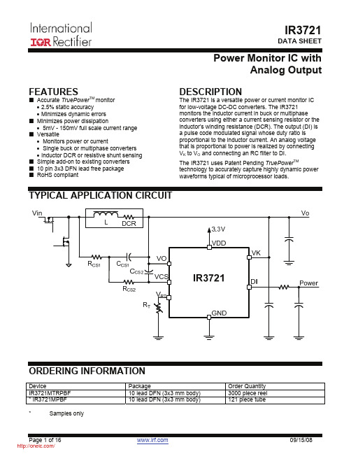
Power Monitor IC withAnalog OutputFEATURESAccurate TruePower TMmonitor • 2.5% static accuracy• Minimizes dynamic errors Minimizes power dissipation• 5mV - 150mV full scale current range Versatile• Monitors power or current• Single buck or multiphase converters • Inductor DCR or resistive shunt sensing Simple add-on to existing converters 10 pin 3x3 DFN lead free package RoHS compliantDESCRIPTIONThe IR3721 is a versatile power or current monitor ICfor low-voltage DC-DC converters. The IR3721 monitors the inductor current in buck or multiphase converters using either a current sensing resistor or the inductor’s winding resistance (DCR). The output (DI) is a pulse code modulated signal whose duty ratio is proportional to the inductor current. An analog voltage that is proportional to power is realized by connecting V K to V O and connecting an RC filter to DI.The IR3721 uses Patent Pending TruePower TMtechnology to accurately capture highly dynamic power waveforms typical of microprocessor loads.TYPICAL APPLICATION CIRCUITORDERING INFORMATIONDevice Package Order Quantity IR3721MTRPBF 10 lead DFN (3x3 mm body) 3000 piece reel * IR3721MPBF 10 lead DFN (3x3 mm body) 121 piece tube* Samples onlyABSOLUTE MAXIMUM RATINGSAbsolute Maximum Ratings (Referenced to GND) VDD:.................................................................3.9V All other Analog and Digital pins......................3.9VOperating Junction Temperature....-10°C to 150°C Storage Temperature Range..........-65°C to 150°C ESD Rating............HBM Class 2 JEDEC Standard MSL Rating..................................................Level 2 Reflow Temperature.....................................260°CStresses beyond those listed under “Absolute Maximum Ratings” may cause permanent damage to the device. These are stress ratings only and functional operation of the device at these or any other conditions beyond those indicated in the operational sections of the specifications are not implied. Exposure to absolute maximum rating conditions for extended periods may affect device reliability.ELECTRICAL SPECIFICATIONSUnless otherwise specified, these specifications apply: VDD = 3.3V ± 5%, 0o C ≤ T J ≤ 125o C, 0.5 ≤ Vo ≤ 1.8 V, and operation in the typical application circuit. See notes following table.NOTES: 1. Guaranteed by designPARAMETER TEST CONDITION MIN TYP MAX UNITBIAS SUPPLYVDD Turn-on Threshold, VDD UP 3.10 V VDD Turn-off Threshold, VDD DN 2.4 V VDD UVLO Hysteresis DI output low when off 75 mV VDD Operating Current, ICC 350 450 μA VOLTAGE REFERENCE V RT Voltage R T = 25.5k Ω 1.452 1.493 1.535 V R T resistance range Note 1 25.5 k Ω ΔΣ CONVERTERVo common mode range 0.5 1.8 V Duty Ratio Accuracy V DCR =20 mV, V O =1V, R T =25.5k Ω, R CS1+R CS2=600 Ω T j =65°C, Note 12.5 %Duty Ratio Accuracy V DCR =20 mV, V O =1V,R T =25.5k Ω, R CS1+R CS2=600 Ω, Note 14 % Sampling frequency, f CLK 435 512 589 kHz Comparator Offset -0.5 +0.5 mV CS pin input current, I CS DI output low -250 +250 nA DIGITAL OUTPUT VK pin voltage range 0.5 1.8 V DI source resistance 1250 2000 3000 ΩBLOCK DIAGRAMVOVGNDIC PIN DESCRIPTIONDESCRIPTIONLEVELI/ONAME NUMBERAnalog Current sensing input, connect through resistor to sensing nodeVCS 1Analog Current sensing reference connect to output voltageVO 2Analog R T thermistor network from this pin to GND programs thermal monitor VRT 3GND 4 Bias return and signal referencesupplybias3.3VVDD 5ICGND 6 Connect to pin 4GND7 Connect to pin 4Analog Power Monitor output; connect to output filterDI 8VK 9 1.8V Connect to fixed voltage or VO, multiplied by DI to become analog output VDD10 3.3V Connect to pin 5BASE PAD Connect to pin 4IC PIN FUNCTIONSVDD PINSThese pins provide operational bias current to circuits internal to the IR3721. Bypass them with a high quality ceramic capacitor to the GND pins.GND PINSThese pins return operational bias current to system ground. VO is measured with respect to GND. The GND pin sinks reference current established by the external resistor R T.VO PINSince this pin measures DCR voltage drop it is critical that it be Kelvin connected to the buck inductor output. Power accuracy may be degraded if the voltage at this pin is below VO min.VCS PINA switched current source internal to the IR3721 maintains the average voltage of this pin equal to the voltage of the VO pin. The average current into this pin is therefore proportional to buck inductor current. VRT PINA voltage reference internal to the IR3721 drives the V RT pin while the pin current is monitored and used to set the amplitude of the current monitor switched current source I REF. Connect this pin to GND through a precision resistor network R T. This network may include provision for canceling the positive temperature coefficient of the buck inductor’s DC resistance (DCR).VK PINThe voltage of the VK pin is used to modulate the amplitude of the DI pin. This is one of the terms used to determine the product of the multiplier output. If VK is connected to a fixed voltage then the output of the multiplier is proportional to current. If VK is connected to the buck converter output voltage then the output of the DI driven RC filter is proportional to power.DI PINThe Dl pin output has a duty ratio proportional to the current into VCS, and an amplitude equal to the voltage at the VK pin. The DI pin is intended to drive an external low pass filter. The output of this filter is the product of the current and voltage terms.FUNCTIONAL DESCRIPTIONPlease refer to the Functional Description Diagram below. Power flow from the buck converter inductor is the product of output voltage times the current I L flowing through the inductor.Power is measured with the aid of InternationalRectifier’s proprietary TruePower™ circuit. Current is converted to a duty ratio that appears at the DI pin. The duty ratio of the DI pin isΤ⋅)+(⋅=R T 2CS 1CS L RATIO DUTY V RR R DCR I DI Equation 1The full-scale current that can be measured corresponds to a duty ratio of one.The amplitude of the DI pin is the voltage appearing at pin VK. If a fixed voltage is applied to VK then the output of the RC filter driven by DI will be proportional to inductor current I L .If VO is applied to V K as shown in the figure then the output of the DI driven RC network will beproportional to power. The full-scale voltage that can be measured is established on the chip to be 1.8V.The full scale power P FS that can be measured is the product of full-scale voltage and full scale current.Figure 1 Functional Description DiagramTHERMAL COMPENSATION FOR INDUCTOR DCR CURRENT SENSINGThe positive temperature coefficient of the inductor DCR can be compensated if R T varies inversely proportional to the DCR. DCR of a copper coil, as a function of temperature, is approximated by)⋅)(+(⋅)(=)(Cu R R TCR T T T DCR T DCR -1Equation 2T R is some reference temperature, usually 25 °C, and TCR Cu is the resistive temperature coefficient ofcopper, usually assumed to be 0.39 %/°C near room temperature. Note that equation 2 is linearly increasing with temperature and has an offset of DCR(T R ) at the reference temperature.If R T incorporates a negative temperature coefficient thermistor then temperature effects of DCR can be minimized. Consider a circuit of two resistors and a thermistor as shown below.RpFigure 2 R T NetworkIf Rth is an NTC thermistor then the value of the network will decrease as temperature increases. Unfortunately, most thermistors exhibit far more variation with temperature than copper wire. One equation used to model thermistors is⎟⎟⎠⎞⎜⎜⎝⎛⎟⎟⎠⎞⎜⎜⎝⎛⋅)(=)(0110TT th th e T R T R - βEquation 3where R th (T) is the thermistor resistance at some temperature T, R th (T 0) is the thermistor resistance at the reference temperature T 0, and β is the material constant provided by the thermistor manufacturer. Kelvin degrees are used in the exponential term of equation 3. If R S is large and R P is small, thecurvature of the equivalent network resistance can be reduced from the curvature of the thermistor alone. Although the exponential equation 3 can nevercompensate linear equation 2 at all temperatures, a spreadsheet can be constructed to minimize error over the temperature interval of interest. Theequivalent resistance R T of the network shown as a function of temperature is)(++=)(T R R R T R th p s T 111Equation 4using R th (T) from equation 3.Equation 2 may be rewritten as a new function of temperature using equations 2 and 4 as follows:())(+⋅)(=)(ΤT DCR R R T R V T I 2CS 1CS T R FS Equation 5With Rs and Rp as additional free variables, use a spreadsheet to solve equation 5 for the desired full scale current while minimizing the I FS (T) variation over temperature.TYPICAL 2-PHASE DCR SENSING APPLICATIONThe IR3721 is capable of monitoring power in a multiphase converter. A Two Phase DCR Sensing Circuit is shown below. The voltage output of any phase is equal to that of any and every other phase because they are electrically connected and monitored at VO as before.Output current is the sum of the two inductor currents (I L1 + I L2). Superposition is used to derive the transfer function for multiphase sensing. The voltage on R CS2 due to I L1 is)||(+)||(⋅⋅3213211CS CS CS CS CS L R R R R R DCR ILikewise, the voltage on RCS2 due to IL2 is)||(+)||(⋅⋅1231222CS CS CS CS CS L R R R R R DCR IThe current through R CS2 due to both inductor currents is I CS . From the two equations above323121122311CS CS CS CS CS CS CS L CS L CS R R R R R R R DCR I R DCR I I +++=The duty ratio of DI isREFTCS DUTYRATIO V R I DI ⋅=If DCR1=DCR2, and RCS1=RCS3, then I CS can be simplified to211212CS CS L L CS R R DCR I I I +⋅)+(=and the DI duty ratio simplifies toΤ⋅)+(⋅⋅)+(=R 2CS 1CS T2L 1L DUTYRATIO V R 2R R DCR I I DIFull scale current occurs when DI duty ratio becomes one.Figure 3 Two Phase DCR Sensing CircuitRESISTOR SENSING APPLICATIONThe Resistor Sensing Circuit shown below is an example of resistive current sensing. Because the voltage on the shunt resistor is directly proportional to the current I L through the inductor, R CS2 and C CS2 do not need to match the L / DCR time constant. Because the value of the shunt resistance does not change with temperature as the inductor DCR does, R T can be a fixed resistor.IFigure 4 Resistor Sensing CircuitCOMPONENT SELECTION GUIDELINES Use a 0.1 μF, 6.3V, X7R ceramic bypass capacitorfrom VDD to GND and from VK to GND.Filter the DI output with an RC filter to give a stable analog representation of the current or power. Some of the DI source resistance of this filter is internal to the IR3721 and specified in the electrical specifications table. Add twenty thousand to fifty thousand additional ohms externally to minimize resistance variation. As the DI source resistance increases beyond these guidelines, the voltage measurement error caused by non-ideal voltmeter conductance will increase.Select a filter capacitor that limits 512 kHz sampling frequency ripple to an acceptable value. Sampling frequency ripple will appear as an error, but can be reduced 20 dB for each decade that the filter corner frequency is below 512 kHz. Select a capacitor value that achieves the desired balance between low sampling frequency ripple and adequate bandwidth. Resistor current sensingFor resistor current sensing select a precision resistor for R T inside the R T resistance range limits specified in the Electrical Specifications table, such as 25.5kΩand 1% tolerance.Next, select a shunt resistor that will provide the most current sensing voltage while also considering the allowable power dissipation limitations. The DI output will saturate to the VK voltage when full scale current I FS flows through this shunt. Recommended maximum current sensing voltage range is 5 to 150 mV. Maximum sensing voltages less than 5 mV will cause comparator input offset voltage errors to dominate, and voltages larger than 150 mV will cause comparator leakage current, I CS, errors to dominate. Select R CS2 to be the next higher standard value resistor from (R SHUNT·I FS·R T) / V RT in order to accommodate full scale current I FS.Bypass VCS to VO with capacitor C CS2. The value of this capacitor limits the bandwidth, but is required because it is the integrator of the delta sigma modulator. Consider selecting the value of C CS2 to place a filter corner frequency at 5 kHz, which will reduce sampling ripple by 40 dB.DCR current sensingSelect an R T network resistance between 20kΩ and 45.3kΩ. Consider the R T network of Figure 5 for DCR current sensing.26.1 kΩ, 1%15.0 kΩ, 1%2.00 kΩ, 1%Murata ThermistorNCP15WB473F03RC47 kΩ, 1%Figure 5 R T networkThe resistance of the network above at 25°C, R T(25), is 37.58kΩ. Over temperature R T(T) is multiplied by copper resistance, DCR(25)·(1+(T-25)·0.0039), divided by (DCR(25)·( R T(25)) to normalize the results, and plotted as nominal error in Figure 6.Figure 6 Nominal error vs. TemperatureNote that the error due to temperature compensation at 25°C is zero, assuming ideal R T components. At other temperatures the results are over or under reported by the factor in percent indicated.Proceed to calculate R SUM, defined as the sum ofR CS1 plus R CS2, as follows.R SUM=I FS·DCR(25) ·R T(25) / V RTAgain, I FS is full scale current and V RT is the reference voltage establishing the current in R T.Estimate the capacitance C CS1 with the following equation.SUMCS R DCR LC ⋅)(⋅>2541Choose a standard capacitor value larger than indicated by the right hand side of the inequality above.Calculate the equivalent resistance R eq .R eq = L / (DCR(25) ·C CS1)We now have two equations, R SUM = R CS1 + R CS2 and Req = (R CS1 · R CS2) / (R CS1 + R CS2). Calculate R CS1 and R CS2 using the following two equations.⎟⎟⎟⎟⎟⎟⎠⎞⎜⎜⎜⎜⎜⎜⎝⎛⋅+⋅=2R R 411R R SUM eq SUM CS1- and⎟⎟⎟⎟⎟⎟⎠⎞⎜⎜⎜⎜⎜⎜⎝⎛⋅⋅=2R R 411R R SUM eq SUM 2CS --Use the next higher standard 1% value than indicated in the equations above. This will insure that full scale current can be measured.Bypass VCS to VO with capacitor C CS2. The value of this capacitor limits the bandwidth, but is required because it is the integrator of the delta sigmamodulator. Consider selecting the value of C CS2 to place a filter corner frequency at 5 kHz, which will reduce sampling ripple by 40 dB.分销商库存信息: IRIR3721MTRPBF。
IRF7105TRPBF中文资料
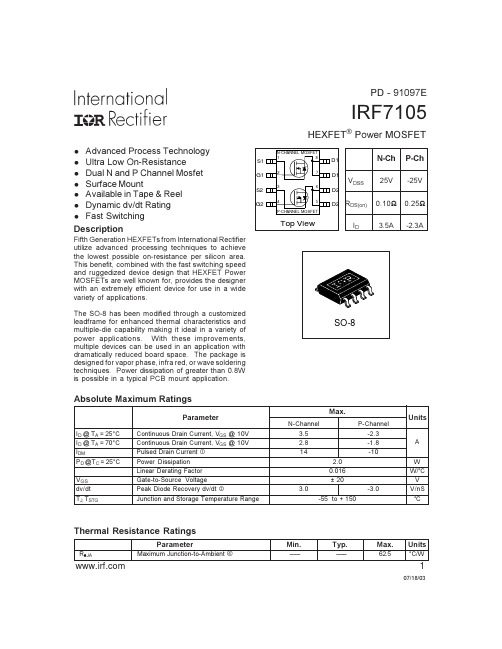
l Advanced Process Technology
l Ultra Low On-Resistance
S1
l Dual N and P Channel Mosfet
G1
l Surface Mount
l Available in Tape & Reel
S2
N-Ch P-Ch 来自41 9075 180
nC
P-Channel
TJ = 25°C, IF = -1.3A, di/dt = 100A/µs
N-P Intrinsic turn-on time is neglegible (turn-on is dominated by LS+LD)
Pulse width ≤ 300µs; duty cycle ≤ 2%.
N-Ch 250 P-Ch 210
pF
N-Ch 61
P-Ch 67
Conditions VGS = 0V, ID = 250µA VGS = 0V, ID = -250µA Reference to 25°C, ID = 1mA Reference to 25°C, ID = -1mA VGS = 10V, ID = 1.0A VGS = 4.5V, ID = 0.50A VGS = -10V, ID = -1.0A VGS = -4.5V, ID = -0.50A VDS = VGS, ID = 250µA VDS = VGS, ID = -250µA VDS = 15V, ID = 3.5A VDS = -15V, ID = -3.5A VDS = 20V, VGS = 0V VDS = -20V, VGS = 0V, VDS = 20V, VGS = 0V, TJ = 55°C VDS = -20V, VGS = 0V, TJ = 55°C VGS = ± 20V
- 1、下载文档前请自行甄别文档内容的完整性,平台不提供额外的编辑、内容补充、找答案等附加服务。
- 2、"仅部分预览"的文档,不可在线预览部分如存在完整性等问题,可反馈申请退款(可完整预览的文档不适用该条件!)。
- 3、如文档侵犯您的权益,请联系客服反馈,我们会尽快为您处理(人工客服工作时间:9:00-18:30)。
ParameterMax.UnitsV DSDrain- Source Voltage30V I D @ T C = 25°C Continuous Drain Current, V GS @ 10V 7.3I D @ T C = 70°C Continuous Drain Current, V GS @ 10V 5.8A I DMPulsed Drain Current 58P D @T C = 25°C Power Dissipation 2.5P D @T C = 70°C Power Dissipation 1.6Linear Derating Factor 0.02W/°C V GS Gate-to-Source Voltage± 20V V GSM Gate-to-Source Voltage Single Pulse tp<10µs 30V E AS Single Pulse Avalanche Energy 70mJ dv/dt Peak Diode Recovery dv/dt5.0V/ns T J, T STGJunction and Storage Temperature Range-55 to + 150°CHEXFET ® Power MOSFETFifth Generation HEXFET ® power MOSFETs from International Rectifier utilize advanced processing techniques to achieve extremely low on-resistance per silicon area. This benefit, combined with the fast switching speed and ruggedized device design that HEXFET MOSFETs are well known for, provides the designer with an extremely efficient and reliable device for use in a wide variety of applications.The SO-8 has been modified through a customized leadframe for enhanced thermal characteristics and multiple-die capability making it ideal in a variety of power applications. With these improvements, multiple devices can be used in an application with dramatically reduced board space. The package is designed for vapor phase, infra red, or wave soldering techniques.Power dissipation of greater than 0.8W is possible in a typical PCB mount application.l Generation V Technology l Ultra Low On-Resistance l N-Channel MOSFET l Surface Mountl Available in Tape & Reel l Dynamic dv/dt Rating l Fast Switching lLead-FreeIRF7201PbFDescription9/30/04ParameterTyp.Max.UnitsR θJAMaximum Junction-to-Ambient–––50°C/WThermal ResistanceAbsolute Maximum RatingsW 1SO-8PD- 95022IRF7201PbFParameterMin.Typ.Max.Units Conditions V (BR)DSSDrain-to-Source Breakdown Voltage 30––––––V V GS = 0V, I D = 250µA∆V (BR)DSS /∆T JBreakdown Voltage Temp. Coefficient –––0.024–––V/°C Reference to 25°C, I D = 1mA ––––––0.030V GS = 10V, I D = 7.3A––––––0.050V GS = 4.5V, I D = 3.7A V GS(th)Gate Threshold Voltage 1.0––––––V V DS = V GS , I D = 250µA g fs Forward Transconductance 5.8––––––S V DS = 15V, ID = 2.3A –––––– 1.0V DS = 24V, V GS = 0V––––––25V DS = 24V, V GS = 0V, T J = 125°C Gate-to-Source Forward Leakage ––––––-100V GS = -20VGate-to-Source Reverse Leakage ––––––100V GS = 20V Q g Total Gate Charge–––1928I D = 4.6A Q gs Gate-to-Source Charge––– 2.3 3.5nC V DS = 24V Q gd Gate-to-Drain ("Miller") Charge ––– 6.39.5V GS = 10V, See Fig. 10 t d(on)Turn-On Delay Time –––7.0–––V DD = 15V t rRise Time–––35–––I D = 4.6At d(off)Turn-Off Delay Time –––21–––R G = 6.2Ωt f Fall Time–––19–––R D = 3.2Ω, C iss Input Capacitance –––550–––V GS = 0V C oss Output Capacitance–––260–––pF V DS = 25V C rssReverse Transfer Capacitance–––100–––ƒ = 1.0MHz, See Fig. 9Electrical Characteristics @ T J = 25°C (unless otherwise specified)I GSS µAΩR DS(on)Static Drain-to-Source On-Resistance I DSS Drain-to-Source Leakage Current nAnsSource-Drain Ratings and CharacteristicsRepetitive rating; pulse width limited bymax. junction temperature. (See fig. 11)I SD ≤ 4.6A, di/dt ≤ 120A/µs, V DD ≤ V (BR)DSS ,T J ≤ 150°CNotes:V DD = 15V, starting T J = 25°C, L = 6.6mHR G = 25Ω, I AS = 4.6A. (See Figure 8)Pulse width ≤ 300µs; duty cycle ≤ 2%.When mounted on 1 inch square copper board, t<10 secIRF7201PbF 3Fig 3. Typical Transfer CharacteristicsFig 2. Typical Output CharacteristicsFig 1. Typical Output Characteristics 1101000.1110DSV , Drain-to-Source Voltage (V)D I , D r a i n -t o -S o u r c e C u r r e n t (A )1101000.1110DSV , Drain-to-Source Voltage (V)D I , D r a i n -t o -S o u r c e C u r r e n t (A )1101003.03.54.04.55.05.5GSV , Gate-to-Source Voltage (V)D I , D r a i n -t o -S o u r c e C u r r e nt (A )Fig 4. Typical Source-Drain DiodeForward Voltage0.11101000.40.60.81.01.2V , Source-to-Drain Voltage (V)I , R e v e r s e D r a i n C u r r e n t (A )SDS DIRF7201PbFFig 5. Normalized On-ResistanceVs. Temperature0.00.51.01.52.0-60-40-2020406080100120140160JT , Junction Temperature (°C)R , D r a i n -t o -S o u r c e O n R e s i s t a n c e D S (o n)(N o r m a l i z e d )Fig 8. Maximum Avalanche EnergyVs. Drain Current04080120160200255075100125150JE , S i n g l e P u l s e A v a l a n c h e E n e r g y (m J )A SStarting T , Junction Temperature (°C)Fig 6. On-Resistance Vs. Drain CurrentFig 7. On-Resistance Vs. Gate Voltage0.020.030.040.05246810121416R , D r a i n -t o -S o u r c e O n R e s i s t a n c e D S (o n)(Ω)GSV , Gate-to-Source Voltage (V)0.000.050.100.150.2010203040I , Drain Current (A)D(Ω)D S (o n)R , D r a i n -t o -S o u r c e O n R e s i s t a n c eIRF7201PbF 5Fig 10. Typical Gate Charge Vs.Gate-to-Source VoltageFig 9. Typical Capacitance Vs.Drain-to-Source Voltage Fig 11. Maximum Effective Transient Thermal Impedance, Junction-to-Ambient02004006008001000110100C , C a p a c i t a n c e (p F )DS V , Drain-to-Source Voltage (V)04812162051015202530Q , Total Gate Charge (nC)GV , G a t e -t o -S o u r c e V o l ta g e (V )G SIRF7201PbFSO-8 Package OutlineIRF7201PbF 7330.00(12.992) MAX.14.40 ( .566 )12.40 ( .488 )NOTES :1. CONTROLLING DIMENSION : MILLIMETER.2. OUTLINE CONFORMS TO EIA-481 & EIA-541.FEED DIRECTIONTERMINAL NUMBER 112.3 ( .484 )11.7 ( .461 )8.1 ( .318 )7.9 ( .312 )NOTES:1. CONTROLLING DIMENSION : MILLIMETER.2. ALL DIMENSIONS ARE SHOWN IN MILLIMETERS(INCHES).3. OUTLINE CONFORMS TO EIA-481 & EIA-541.SO-8 Tape and ReelDimensions are shown in milimeters (inches)Data and specifications subject to change without notice.This product has been designed and qualified for the Consumer market.Qualifications Standards can be found on IR’s Web site.IR WORLD HEADQUARTERS: 233 Kansas St., El Segundo, California 90245, USA Tel: (310) 252-7105TAC Fax: (310) 252-7903Visit us at for sales contact information .09/04分销商库存信息:IRIRF7201TRPBF IRF7201PBF。