MMA2301D中文资料
APM2301中文资料
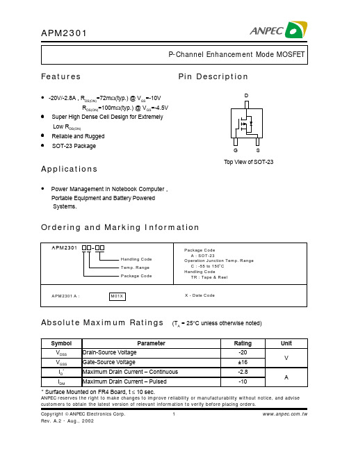
ANPEC reserves the right to make changes to improve reliability or manufacturability without notice, and advise customers to obtain the latest version of relevant information to verify before placing orders.Pin DescriptionOrdering and Marking InformationFeaturesApplicationsAbsolute Maximum Ratings (T A = 25°C unless otherwise noted)• -20V/-2.8A , R DS(ON)=72m Ω(typ.) @ V GS =-10VR DS(ON)=100m Ω(typ.) @ V GS =-4.5V• Super High Dense Cell Design for ExtremelyLow R DS(ON)• Reliable and Rugged • SOT-23 Package• Power Management in Notebook Computer ,Portable Equipment and Battery Powered Systems.* Surface Mounted on FR4 Board, t ≤ 10 sec.G DSTop View of SOT-23Notesa : Pulse test ; pulse width ≤300µs, duty cycle ≤ 2%b: Guaranteed by design, not subject to production testingAbsolute Maximum Ratings Cont. (T A = 25°C unless otherwise noted)Electrical Characteristics (T A = 25°C unless otherwise noted)2468100.0300.0450.0600.0750.0900.1050.1200.1350.150012345246810-50-2502550751001251500.000.250.500.751.001.251.500.00.5 1.0 1.5 2.0 2.50246810Typical Characteristics-I D -D r a i n C u r r e n t (A )Transfer Characteristics-V GS - Gate-to-Source Voltage (V)Threshold Voltage vs. Junction T emperatureTj - Junction T emperature (°C)-V G S (t h )-T h r e s h o l d V o l t a g e (V )(N o r m a l i z e d )R D S (O N )-O n -R e s i s t a n c e (Ω)On-Resistance vs. Drain Current-I D - Drain Current (A)Output Characteristics-I D -D r a i n C u r r e n t (A )-V DS - Drain-to-Source Voltage (V)369121505101520-50-25025507510012515012345678910Typical CharacteristicsR D S (O N )-O n -R e s i s t a n c e (Ω)(N o r m a l i z e d )On-Resistance vs. Junction TemperatureT J - Junction Temperature (°C)-V DS - Drain-to-Source Voltage (V)CapacitanceC a p a c i t a n c e (p F )-V GS - Gate-to-Source Voltage (V)R D S (O N )-O n -R e s i s t a n c e (Ω)On-Resistance vs. Gate-to-Source VoltageGate ChargeQ G - Gate Charge (nC)-V G S -G a t e -S o u r c e V o l t a g e (V )0.00.20.40.60.8 1.0 1.2 1.4 1.61100.010.1110100024681012141E-41E-30.010.11101000.010.11Typical CharacteristicsP o w e r (W )Single Pulse PowerTime (sec)Square Wave Pulse Duration (sec)Source-Drain Diode Forward Voltage-I S -S o u r c e C u r r e n t (A )-V SD -Source-to-Drain Voltage (V)N o r m a l i z e d E f f e c t i v e T r a n s i e n t T h e r m a l I m p e d a n c eNormalized Thermal Transient Impedence, Junction to AmbientPackaging Information SOT-23Physical SpecificationsReflow Condition (IR/Convection or VPR Reflow)Reference JEDEC Standard J-STD-020A APRIL 1999Classification Reflow ProfilesPackage Reflow ConditionsPre-heat temperature183 CPeak temperatureTime°t e m p e r a t u r eReliability test programCarrier Tape & Reel DimensionsCover Tape DimensionsCustomer ServiceAnpec Electronics Corp.Head Office :5F, No. 2 Li-Hsin Road, SBIP,Hsin-Chu, T aiwan, R.O.C.T el : 886-3-5642000Fax : 886-3-5642050Taipei Branch :7F, No. 137, Lane 235, Pac Chiao Rd.,Hsin Tien City, Taipei Hsien, T aiwan, R. O. C.T el : 886-2-89191368Fax : 886-2-89191369。
SAE AMS 2301-2001- 中文
端要首先磁化检验,较大的台阶要分别单独磁化并检验直到所有的台阶都检验完。如果
板状的用的是长薄片(如 3.1.3.5),只检验长薄片的两个面
3.2.1 清洁度标准主要要检验非金属夹杂物(见 8.3),除了样品制作过程中造成的裂缝重叠
等缺陷外,其余的裂纹等缺陷会被拒收
3.2.2 磁粉探伤检验要做记录,记录填写后,买方可要求查看
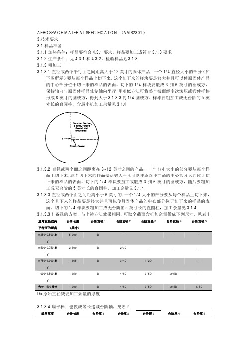
3.1.3.2 直径或两个面之间距离在 6~12 英寸之间的产品:一个 1/4 大小的部分要从每个样 品上切下来,这个切下来的样品要足够大并且可以使原固体产品的中心部分大约位于切
下来的样品的表面。切下的 1/4 样块要加工或锻成 3 到 6 英寸的圆或方,随后要粗加 工成无台阶的 5 英寸长的直圆柱,加工余量见 3.1.4 3.1.3.3 直径或两个面之间距离小于 6 英寸的:一个 1/4 大小的部分要从每个样品上切下来, 这个且下来的样品要足够大并且可以使原固体产品的中心部分位于切下来的样品的表
T
T=原始通常减去加工余量的厚度
--
--
--
--
2/3T
--
--
--
3/4T
1/2T
1/4T
--
4/5T
3/5T
2/5T
1/5T
3.1.3.5 厚板或平板:要加工一个直圆柱或矩形,或者锻造后加工,样棒要从滚压的平行方 向取,要位于板宽的中心到边缘的中部,大约 5 英寸长,不大于 4 英寸直径或厚度。
含碳量(%)
频次等级
小于 0.25
0.37
大于等于 0.25
0.34
严重性等级 0.28 0.25
3.4.1.2 板类的符合表 8 频次等级(同一 热处理) 0.80
美国MOTOROLA 压力传感器说明书

美国MOTOROLA压力传感器美国MOTOROLA公司的MPX系列硅压力传感器,主要以气压测量为主,适合用于医疗器械,气体压力控制等领域,输出数字信号。
其测量方式可分为:表压(GP)、绝压(A、AP)、差压(D、DP)型。
在宽温度范围工作时需外加补偿网络和信号调整电路。
具体型号分类而定名称:MPX2010DP 名称:MPX5700DP MPX5700GP 名称:MPX2100AP名称:MPX5500DP 名称:MPX5100AP 名称:MPX5050DP名称:MPX5010DP 名称:MPX4115AP 名称:MPX2200A 名称:MPX2200AP 名称:MPXH6115A6U 名称:MPX4250DP名称:MPX4115A 名称:MPX2202DP 名称:MPX2102AP名称:MPX2053GP 名称:MPXY8300A6U 压力传感器 名称:触力型压力传感器 FSG15N1A 名称:硅压力传感器 MPXH6115A 名称:MPX5700DP 硅压力传感器 名称:MPX53GP 硅压力传感器 名称:压力传感器FPM07 名称:轮胎压力传感器TP015 名称:轮胎压力传感器NPP301名称:Freescale 压力传感器 MPX2010DP商斯达实业传感器与智能控制分公司专门从事各种进口传感器的营销工作,代理多家欧美知名公司的产品。
涉及压力、温度、湿度、电流、液位、磁阻、霍尔、流量、称重、光纤、倾角、扭矩、气体、光电、位移、触力、红外、速度、加速度等多种产品。
广泛应用于航空航天、医疗器械(如血压计)、工业控制、冶金化工、汽车制造、教育科研等领域。
商斯达实业代理的品牌产品主要有:压 力:Kulite、ACSI、Honeywell、Entran、Gems、Dwyer、SSI、Smi、Senstronics、Intersema、Motorola、 NAIS、E+H、Fujikura、Dytran、APM称重测力:Transcell、HBM、Interface、Thamesside、Philips、Entran 温 湿 度:Honeywell、Dwyer流 量:Gems、Dwyer、Honeywell、Folwline、WorldMagnetics 液 位:Honeywell、Siccom、Gems、Dwyer、Kulite、SSI 加 速 度:Entran、Silicondesigns、Dytran 压力开关:ACSI、Gems、Dwyer、台湾矽微航空器材:TexTech 隔音材料、Honeywell 薄膜加热片、DigirayX 射线探伤仪 仪 表:Honeywell、Transcell、东辉、上润、AD、东崎商斯达实业 除代理上述产品外,还有几条传感器生产线,一条压力传感器组装线,可为用户提供各种用途的、特殊要求的配套产品。
MSP2301摩矽P沟道MOS管规格书
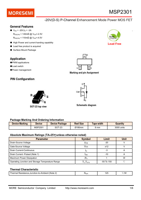
-20V(D-S) P-Channel Enhancement Mode Power MOS FETGeneral Features● V DS = -20V,I D = -3AR DS(ON) < 140m Ω @ V GS =-2.5V R DS(ON) < 110m Ω @ V GS =-4.5V● High Power and current handing capability ● Lead free product is acquired ● Surface Mount PackageApplication●PWM applications ●Load switch ●Power managementSchematic diagramMarking and pin AssignmentSOT-23 top viewPackage Marking And Ordering InformationDevice MarkingDevice Device PackageReel Size Tape width Quantity MSP2301SOT-23Ø180mm8 mm3000 unitsAbsolute Maximum Ratings (TA=25℃unless otherwise noted)Parameter Symbol Limit UnitDrain-Source Voltage V DS -20 V Gate-Source Voltage V GS±12 V Drain Current-Continuous I D -3 A Drain Current -Pulsed (Note 1) IDM -10 A Maximum Power Dissipation P D 1 W Operating Junction and Storage Temperature Range T J ,T STG -55 To 150 ℃Thermal CharacteristicThermal Resistance,Junction-to-Ambient (Note 2)R θJA125/W ℃Lead FreePIN ConfigurationGate-Body Leakage Current I GSS V GS =±12V,V DS =0V - - ±100nA On Characteristics (Note 3) Gate Threshold VoltageV GS(th) V DS =V GS ,I D =-250μA -0.4 -0.7 -1 V V GS =-4.5V, I D =-3A - 64 110 m Ω Drain-Source On-State Resistance R DS(ON) V GS =-2.5V, I D =-2A -89 140 m Ω Forward Transconductance g FSV DS =-5V,I D =-2.8A - 9.5 - SDynamic Characteristics (Note4) Input Capacitance C lss - 405 - PF Output CapacitanceC oss - 75 - PFReverse Transfer Capacitance C rssV DS =-10V,V GS =0V,F=1.0MHz- 55 - PF Switching Characteristics (Note 4) Turn-on Delay Time t d(on) - 11 - nSTurn-on Rise Time t r - 35 - nS Turn-Off Delay Time t d(off) - 30 - nSTurn-Off Fall Time t fV DD =-10V,I D =-1A V GS =-4.5V,R GEN =10Ω - 10 - nSTotal Gate Charge Q g - 3.3 12 nCGate-Source Charge Q gs - 0.7 - nCGate-Drain ChargeQ gd V DS =-10V,I D =-3A,V GS =-2.5V- 1.3 - nC Drain-Source Diode Characteristics Diode Forward Voltage (Note 3) V SDV GS =0V,I S =1.3A - - -1.2 VDiode Forward Current (Note 2)I S - - -1.3 ANotes:1. Repetitive Rating: Pulse width limited by maximum junction temperature.2. Surface Mounted on FR4 Board, t ≤ 10 sec.3. Pulse Test: Pulse Width ≤ 300μs, Duty Cycle ≤ 2%.4. Guaranteed by design, not subject to productionElectrical Characteristics (TA=25℃unless otherwise noted)ParameterSymbol Condition Min Typ Max UnitOff CharacteristicsDrain-Source Breakdown VoltageBV DSS V GS =0V I D =-250μA -20 -24 - V Zero Gate Voltage Drain Current I DSS V DS =-20V,V GS =0V - - -1 μATYPICAL ELECTRICAL AND THERMAL CHARACTERISTICSFigure 1:Switching Test CircuitT J -Junction Temperature(℃)Figure 3 Power DissipationVds Drain-Source Voltage (V)Figure 5 Output CHARACTERISTICSV INV tFigure 2:Switching WaveformsT J -Junction Temperature(℃)Figure 4 Drain CurrentI D - Drain Current (A)Figure 6 Drain-Source On-ResistanceP D P o w e r (W )I D - D r a i n C u r r e n t (A )R d s o n O n -R e s i s t a n c e (Ω)I D - D r a i n C u r r e n t (A )Vgs Gate-Source Voltage (V)Figure 7 Transfer CharacteristicsVgs Gate-Source Voltage (V)Figure 9 Rdson vs VgsQg Gate Charge (nC)Figure 11 Gate ChargeT J -Junction Temperature(℃)Figure 8 Drain-Source On-ResistanceVds Drain-Source Voltage (V)Figure 10 Capacitance vs VdsVsd Source-Drain Voltage (V)Figure 12 Source- Drain Diode ForwardI D - D r a i n C u r r e n t (A )R d s o n O n -R e s i s t a n c e (Ω)V g s G a t e -S o u r c e V o l t a g e (V )N o r m a l i z e d O n -R e s i s t a n c e C C a p a c i t a n c e (p F )I s - R e v e r s e D r a i n C u r r e n t (A )Vds Drain-Source Voltage (V)Figure 13 Safe OperationAreaSquare Wave Pluse Duration(sec)Figure 14 Normalized Maximum Transient Thermal Impedancer (t ),N o r m a l i z e d E f f e c t i v eT r a n s i e n t T h e r m a l I m p e d a n c eI D - D r a i n C u r r e n t (A )SOT-23 PACKAGE INFORMATIONDimensions in Millimeters (UNIT:mm)Dimensions in MillimetersSymbolMIN. MAX.A 0.900 1.150A1 0.000 0.100A2 0.900 1.050b 0.300 0.500c 0.080 0.150D 2.800 3.000E 1.200 1.400E1 2.250 2.550e 0.950TYPe1 1.800 2.000L 0.550REFL1 0.300 0.500θ 0° 8°NOTES1. All dimensions are in millimeters.2. Tolerance ±0.10mm (4 mil) unless otherwise specified3. Package body sizes exclude mold flash and gate burrs. Mold flash at the non-lead sides should be less than 5 mils.4. Dimension L is measured in gauge plane.5. Controlling dimension is millimeter, converted inch dimensions are not necessarily exact.。
2301D调速器文说明书

Installation and Operation Manual2301D Digital Load Sharing and Speed Control for EnginesOrdinary Locations—8273-101 Hazardous Locations—8273-135, -1000Manual 26065 (Revision H)DEFINITIONSThis is the safety alert symbol. It is used to alert you to potential personal injury hazards. Obey all safety messages that follow this symbol to avoidpossible injury or death.•DANGER—Indicates a hazardous situation which, if not avoided, will result in deathor serious injury.•WARNING—Indicates a hazardous situation which, if not avoided, could result indeath or serious injury.•CAUTION—Indicates a hazardous situation which, if not avoided, could result inminor or moderate injury.•NOTICE—Indicates a hazard that could result in property damage only (includingdamage to the control).•IMPORTANT—Designates an operating tip or maintenance suggestion.The engine, turbine, or other type of prime mover should be equipped with anoverspeed shutdown device to protect against runaway or damage to the primemover with possible personal injury, loss of life, or property damage.The overspeed shutdown device must be totally independent of the prime movercontrol system. An overtemperature or overpressure shutdown device may alsobe needed for safety, as appropriate.Read this entire manual and all other publications pertaining to the work to be performed beforeinstalling, operating, or servicing this equipment. Practice all plant and safety instructions andprecautions. Failure to follow instructions can cause personal injury and/or property damage.This publication may have been revised or updated since this copy was produced. To verify thatyou have the latest revision, be sure to check the Woodward website:/pubs/current.pdfThe revision level is shown at the bottom of the front cover after the publication number. The latestversion of most publications is available at:/publicationsIf your publication is not there, please contact your customer service representative to get thelatest copy.Any unauthorized modifications to or use of this equipment outside its specified mechanical,electrical, or other operating limits may cause personal injury and/or property damage, includingdamage to the equipment. Any such unauthorized modifications: (i) constitute "misuse" and/or"negligence" within the meaning of the product warranty thereby excluding warranty coveragefor any resulting damage, and (ii) invalidate product certifications or listings.To prevent damage to a control system that uses an alternator or battery-chargingdevice, make sure the charging device is turned off before disconnecting the batteryfrom the system.To prevent damage to electronic components caused by improper handling, readand observe the precautions in Woodward manual 82715, Guide for Handling andProtection of Electronic Controls, Printed Circuit Boards, and Modules. Revisions—Text changes are indicated by a black line alongside the text.Woodward Governor Company reserves the right to update any portion of this publication at any time. Informationprovided by Woodward Governor Company is believed to be correct and reliable. However, no responsibility is assumedby Woodward Governor Company unless otherwise expressly undertaken.© Woodward 2000All Rights ReservedManual 26065 2301D Digital ControlWoodward i ContentsR EGULATORY C OMPLIANCE ....................................................................... IV E LECTROSTATIC D ISCHARGE A WARENESS ................................................. VI C HAPTER 1. G ENERAL I NFORMATION .. (1)Description (1)Applications (2)Control Options (2)References ............................................................................................................. 3 C HAPTER 2. I NSTALLATION .. (9)Introduction (9)Unpacking (9)Power Requirements (9)Location Considerations (9)Electrical Connections (10)Shields and Grounding (10)Setting Speed Range (11)Potential Transformer Connections (11)Current Transformer Connections (11)Load Sharing Lines (12)Power Supply (12)Discrete Inputs (Terminals 28–38) (13)Close to Run or Minimum Fuel (Terminal 31) (13)Failed Speed Signal Override (Terminal 32) (14)Rated Speed (Terminal 33) (14)CB Aux/Droop Contact (Terminal 34) (14)Raise Speed/Load Contact (Terminal 35) (15)Lower Speed/Load Contact (Terminal 36) (16)Load Generator (Terminal 37) (16)Base Load (Terminal 38) (16)Actuator Output (16)Speed and Phase Matching (SPM) Synchronizer (17)(Analog Input #1; Terminals 19-20) (17)Remote Speed/Load Set Point/Auxiliary Input (17)(Analog Input #2; Terminals 22-23) (17)Speed Sensor (17)Relay Driver Outputs (Terminals 41–44) (18)Analog Output #1 (Terminals 16-17) (18)RS-232 Communication Port (18)Installation Check-out Procedure ......................................................................... 19 C HAPTER 3. E NTERING C ONTROL S ET P OINTS . (20)Introduction (20)Watch Window PC Interface (20)Configure Menu Descriptions (22)Service Menu Descriptions (24)I** ANALOG INPUTS SETTINGS ** (37)Adjust For Stable Operation (43)Speed Setting Adjustment (43)Dynamic Adjustment (44)Actuator Compensation Adjustment (44)Low Idle Speed Adjustment (44)2301D Digital Control Manual 26065ii WoodwardContentsRamp Time Adjustment (44)Raise/Lower Time Adjustment (45)Start Fuel Limit Adjustment (45)Speed Sensor Check (45)Current Transformer (CT) Phasing Check (45)Phase Correction Procedure (46)Load Calibration Adjustment (49)Droop Adjustment ................................................................................................. 49 C HAPTER 4. D ESCRIPTION OF O PERATION .. (50)Introduction (50)Speed Control (50)Control Dynamics (51)Minimum Fuel Function (52)Maximum Fuel Function (53)Start Limit Function (53)Speed/Load Reference and Ramps (54)Speed Reference and Ramp Functions (54)Speed Bias and Synchronizer Summing (55)Load Reference and Ramp Functions (56)Droop Function ..................................................................................................... 58 C HAPTER 5. T ROUBLESHOOTING (64)Introduction (64)Troubleshooting Procedure (64)Control Start-up (64)Control Test and Calibration ................................................................................. 65 C HAPTER 6. S ERVICE O PTIONS (72)Product Service Options (72)Woodward Factory Servicing Options (73)Returning Equipment for Repair (74)Replacement Parts (74)Engineering Services (75)How to Contact Woodward (75)Technical Assistance ............................................................................................ 76 A PPENDIX . S ERVICE /C ONFIGURE C HART .................................................... 77 2301D C ONTROL S PECIFICATIONS . (82)D ECLARATIONS .........................................................................................83Manual 26065 2301D Digital ControlWoodward iii Illustrations and TablesFigure 1-1a. 2301D Outline Drawing (Ordinary Locations) (4)Figure 1-1b. 2301D Outline Drawing (Hazardous Locations) (5)Figure 1-2. 2301D Plant Wiring Diagram (sheet 1) (6)Figure 1-2. 2301D Plant Wiring Diagram (sheet 2) (7)Figure 1-2. 2301D Plant Wiring Diagram (notes) (8)Figure 2-1. Installation of Wiring into Terminal (11)Figure 2-2. Droop Contact and Circuit Breaker Auxiliary Contact (15)Figure 3-1. Control Gain as a Function of Speed Error (25)Figure 3-2. Speed Filter (26)Figure 3-3. Typical Transient Response Curves (27)Figure 3-4. Non-linear Valve Power Curve (30)Figure 3-5. Sample Engine Plot (31)Figure 3-6. Linearized Gain Plot (31)Figure 3-7. Start Limit Function (34)Figure 3-8. Temporary Wiring for Transformer Phase Correction (47)Figure 3-9. Droop Adjustment (49)Figure 4-1. Speed Control System (51)Figure 4-2. Start Limit Function (53)Figure 4-3. Remote Speed Reference (55)Figure 4-4. Paralleling System (59)Figure 4-5. Droop Mode (60)Figure 4-6. Isochronous Mode (61)Figure 4-7. Droop/Isochronous Load Sharing (62)Figure 4-8. Isochronous Load Sharing (62)Table 4-1. Description of Discrete Inputs While in Load Control (58)2301D Digital Control Manual 26065iv WoodwardRegulatory ComplianceEuropean Compliance for CE Mark:EMC Directive Declared to 89/336/EEC COUNCIL DIRECTIVE of03 May 1989 on the approximation of the laws of themember states relating to electromagneticcompatibility.Low Voltage Directive Declared to the 73/23/EEC COUNCIL DIRECTIVE of19 February 1973 on the harmonization of the lawsof the Member States relating to electricalequipment designed for use within certain voltagelimits.North American Compliance:CSA Certified for Class I, Division 2, Groups A, B, C, D,T4 Hazardous Locations and non-hazardouslocations at 70 °C ambient . Certified for UnitedStates and Canada.Certificate 1150575UL Listed for Ordinary Locations for use in the UnitedStates and Canada.UL File E97763NOTE: Wiring must be in accordance with applicable electric codes with theauthority having jurisdiction.These listings are limited only to those units bearing the CSA or UL agencyidentification and the Hazardous or Ordinary Locations markings.Marine Compliance:Bureau Veritas BV Rules Part C, June 2000Det Norske Veritas Standard for Certification, No. 2.4.2001Germanischer Lloyd Additional Rules and Guidelines, Part 1,2001Lloyd’s Register of Shipping Type Approval System, Test SpecificationNumber 1, 2002Registro Italiano Navale RINA Rules 2001 – Part CNOTE: These certifications apply to specific models only.The 2301D is suitable for use in Class I, Division 2, Groups A, B, C, and D perCSA for Canada and US or non-hazardous locations only. These listings arelimited only to those units bearing the CSA agency identification and hazardous location markings.The 2301D is suitable for use in Ordinary Locations per UL and CSA for Canada and US or non-hazardous locations only. These listings are limited only to those units bearing the UL and CSA agency identification and ordinary locationmarkings.Wiring must be in accordance with North American Class I, Division 2 wiringmethods as applicable, and in accordance with the authority having jurisdiction.Connector J1 must not be used in hazardous locations.The 2301D must be installed in a suitable enclosure. The final combination shall be approved by a local authority having jurisdiction.Marine certified models available.Manual 26065 2301D Digital ControlWoodward vEXPLOSION HAZARD—Do not remove covers or connect/disconnectelectrical connectors unless power has been switched off or the area is knownto be non-hazardous.Substitution of components may impair suitability for Class I, Division 2.RISQUE D’EXPLOSION—Ne pas enlever les couvercles, niraccorder / débrancher les prises électriques, sans vous enassurez auparavant que le système a bien été mis hors tension;ou que vous vous situez bien dans une zone non explosive.La substitution de composants peut rendre ce matérielinacceptable pour les emplacements de Classe I, Division 2.2301D Digital Control Manual 26065vi WoodwardElectrostatic Discharge AwarenessAll electronic equipment is static-sensitive, some components more than others. To protect these components from static damage, you must take specialprecautions to minimize or eliminate electrostatic discharges.Follow these precautions when working with or near the control.1. Before doing maintenance on the electronic control, discharge the staticelectricity on your body to ground by touching and holding a grounded metalobject (pipes, cabinets, equipment, etc.).2. Avoid the build-up of static electricity on your body by not wearing clothingmade of synthetic materials. Wear cotton or cotton-blend materials as muchas possible because these do not store static electric charges as much assynthetics.3. Keep plastic, vinyl, and Styrofoam materials (such as plastic or Styrofoamcups, cup holders, cigarette packages, cellophane wrappers, vinyl books orfolders, plastic bottles, and plastic ash trays) away from the control, themodules, and the work area as much as possible.4. Do not remove the printed circuit board (PCB) from the control cabinetunless absolutely necessary. If you must remove the PCB from the controlcabinet, follow these precautions:• Do not touch any part of the PCB except the edges.• Do not touch the electrical conductors, the connectors, or thecomponents with conductive devices or with your hands.• When replacing a PCB, keep the new PCB in the plastic antistaticprotective bag it comes in until you are ready to install it. Immediatelyafter removing the old PCB from the control cabinet, place it in theantistatic protective bag.To prevent damage to electronic components caused by improperhandling, read and observe the precautions in Woodward manual82715, Guide for Handling and Protection of Electronic Controls,Printed Circuit Boards, and Modules .Manual 26065 2301D Digital ControlWoodward 1 Chapter 1.General InformationDescriptionThe Woodward 2301D controls load sharing and speed of generators driven by diesel or gaseous engines. (These power sources are referred to as “primemovers” throughout this manual.) The 2301D is a microprocessor-based digital control designed to include the functions of and be compatible with 2301A load sharing controls. The increased flexibility of software allows the 2301D to include control functions that required additional equipment in previous versions of2301A control systems. The 2301D therefore is suitable for upgrading existingcontrol systems or increased functionality in new installations.The control is housed in a sheet-metal chassis and consists of a single printedcircuit board. The 2301D is set up and configured through an external computer connected at the 9-pin connector at the front of the control. The configurationsoftware is supplied with each control.The 2301D provides control in either isochronous, droop, or base load. The2301D will allow for soft load transfer when being added to or removed from abus.The isochronous mode is used for constant prime mover speed with:• Single prime mover operation or• Two or more prime movers controlled by Woodward load sharing controlsystems on an isolated busThe droop mode is used for speed control as a function of load with:• Single prime mover operation on an infinite bus or• Parallel operation of two or more prime moversThe base load mode provides constant load level operation against a bus withthe load controlled by the 2301D.• The load setting is set by a fixed reference,• or an external input analog input,• or external contact control of the reference.The 2301D Control Hardware includes:• 1 Load Sensor• 1 Actuator Driver• 1 MPU Speed Sensor• 1 Configurable Analog Output• 2 Configurable Analog Inputs• 8 Discrete (Switch) Inputs• 4 Discrete (Relay Driver) OutputsThe following is an example of the typical hardware needed for a 2301D system controlling a single prime mover and generator:• A 2301D electronic control• An external 18 to 40 Vdc power source• A speed-sensing device• A proportional actuator to position the fuel-metering device and• Current and potential transformers for measuring the load carried by thegenerator2301D Digital Control Manual 260652 Woodward The engine and generator synchronous speed (50 or 60 Hz GeneratorFrequency) needs to be within 300 to 3600 rpm. The frequency from themagnetic pickup must be within the range of 100 to 20 000 Hz at rated speed.The 2301D speed range needs to be configured using an external computerduring installation.These 2301D controls operate with an input of 18 to 40 Vdc.ApplicationsBecause of the configuration software available in the 2301D hardware,application variations can now be selected using an external computer. Changing the application to accommodate engine speed range, gear teeth, and selection of forward or reverse acting actuator is a matter of software setup rather thanchanging hardware. See Chapter 3 to enter control set points.The speed range is factory set for 900 rpm, 450 Hz. Using the wrongspeed configuration could cause an overspeed with resulting damage to equipment or personal injury or death.The 2301D Control can be configured for forward- or reverse-acting applications. In reverse-acting systems, the actuator calls for more fuel when the actuatorvoltage decreases. Complete loss of voltage to the actuator will drive the actuator to full fuel. This allows a backup mechanical ballhead governor to take control rather than shut down the prime mover as would a direct-acting system.External wiring connections for reverse-acting controls are identical to those for direct-acting controls.Control OptionsHere is a brief summary of programmable options in addition to speed range and actuator type:• Actuator current range 0–20 mA, 4–20 mA, 0–200 mA.• Speed trim with external raise and lower switches. Tunable rates.•External setting of analog speed reference input or an external analog baseload reference.• Multiple dynamics options—single dynamics settingselection of 2 sets of dynamics switched with Circuit Breaker Aux input 5 slope gain settingserror window gain ratio• Start fuel limiter• Analog output• Discrete outputsWoodward application engineers are always available to assist you in selection of the correct control for your system, or to answer questions concerning control installation, operation, or calibration. Contact any Woodward office.ReferencesThe following publications contain additional product or installation information on Load Sharing and Speed Controls, and related components. They can be ordered from any Woodward office.Manual Title25070 Electric Governor Installation Guide25195 Governing Fundamentals82384 SPM-A Synchronizer82510 Magnetic Pickups and Proximity Switches for Electric Governors 82715 Guide for Handling and Protection of Electronic Controls, Printed Circuit Boards, and Modules26007 Woodward Watch Window Software Getting StartedProductSpec Title03204 2301D Digital 2301 Control82383 SPM-A Synchronizer82516 EG3P/3PC Actuator82575 EGB1P/2P Governor/ActuatorFigure 1-1a. 2301D Outline Drawing (Ordinary Locations)Figure 1-1b. 2301D Outline Drawing (Hazardous Locations)Figure 1-2. 2301D Plant Wiring Diagram (sheet 1)Figure 1-2. 2301D Plant Wiring Diagram (sheet 2)Figure 1-2. 2301D Plant Wiring Diagram (notes)Chapter 2.InstallationIntroductionThis chapter contains general installation instructions for the 2301D control.Power requirements, environmental precautions, and location considerations are included to determine the best location for the control. Additional informationincludes unpacking instructions, electrical connections, and an installation check-out procedure.UnpackingBefore handling the control, read page iv, “Electrostatic Discharge Awareness”.Be careful when unpacking the electronic control. Check the control for signs of damage such as bent or dented panels, scratches, and loose or broken parts. Ifany damage is found, immediately notify the shipper.Power RequirementsThe 2301D control requires a voltage source of 18 to 40 Vdc, with a currentcapacity of at least 900 mA for operating power. If a battery is used for operating power, an alternator or other battery charging device is necessary to maintain astable supply voltage.To prevent damage to the control, make sure that the alternator orother battery-charging device is turned off or disconnected beforedisconnecting the battery from the control.Location ConsiderationsThis product is intended for installation in a “closed electrical operatingarea” or in an enclosed industrial control cabinet. Consider theserequirements when selecting the mounting location:•Adequate ventilation for cooling•Space for servicing and repair•Protection from direct exposure to water or to a condensation-prone environment•Protection from high-voltage or high-current devices, or devices which produce electromagnetic interference•Avoidance of vibration•Selection of a location that will provide an operating temperature range of –40 to +70 °C (–40 to +158 °F)•The control must NOT be mounted on the engine.Electrical ConnectionsAll inputs and outputs are made through screwless spring-actuated terminalblocks. For EMI reasons, it is recommend that all low-current wires be separatedfrom all high-current wire.The spring clamp can be actuated by using a standard 2.5 mm or 3/32 inch flatbladed screwdriver. The terminal blocks accept wires from 0.08–4 mm² (27–12AWG). Two 18 AWG or three 20 AWG wires can be easily installed in eachterminal. Wires for the fixed mounted power terminals should be stripped 5–6mm (0.22 inch) long.Do not tin (solder) the wires that terminate at the terminal blocks. Thespring-loaded terminal blocks are designed to flatten stranded wire,and if those strands are tinned together, the connection losessurface area and is degraded.Shields and GroundingAn individual shield termination is provided at the terminal block for each of thesignals requiring shielding. All of these inputs should be wired using shielded,twisted-pair wiring. The exposed wire length beyond the shield should be limitedto one 25 mm (1 inch). Relay outputs, contact inputs, and power supply wiring donot normally require shielding, but can be shielded if desired.The 2301D is designed for shield termination to earth ground at the control. Ifintervening terminal blocks are used in routing a signal, the shield should becontinued through the terminal block. If shield grounding is desired at theterminal block, it should be ac coupled to earth. All other shield terminationsexcept at the control should be ac coupled to earth through a capacitor. A 1000pF, 500 V capacitor is sufficient. The intent is to provide a low impedance path toearth for the shield at frequencies of 150 kHz and up. Multiple direct connectionsof a shield to earth risk high levels of current to flow within the shield (exception,see note below on cabinet installations).Shields can be grounded at both ends (2301D and load) if the cable length issufficiently short (i.e. within a cabinet) to prevent ground loop current in theshield.Cabinet Installations: If the 2301D is installed in a cabinet, shieldedI/O can be terminated directly to the cabinet (earth ground) at theentry to the cabinet, as well as at the control.For EMC reasons, it is recommend that all low-current wires beseparated from all high-current wires. Input Power ground terminalshould also be wired to earth ground.Figure 2-1. Installation of Wiring into TerminalSetting Speed RangeThe Microprocessor inside the 2301D calculates the speed range to be used byentering the engine/generator synchronous speed and number of gear teeth.This configured speed sets the hardware-to-software scaling. The rated speedsetting is set in service as the speed reference selected when the Rated switch is closed..The number of gear teeth is used by the control to convert pulsesfrom the speed sensing device to engine rpm. To prevent possibleserious injury from an overspeeding engine, make sure the control isproperly programmed to convert the gear-tooth count into enginerpm. Improper conversion could cause engine overspeed.The speed range is factory set for 450 Hz, 900 rpm (30 teeth). Refer toChapter 3 to change speed range and prevent possible overspeed.Using the wrong speed range could cause an overspeed withresulting damage to equipment or personal injury or death.Potential Transformer ConnectionsConnect the potential transformer secondary leads to the following terminals: Phase A to terminal 1Phase B to terminal 2Phase C to terminal 3The potential transformer secondary line-to-line voltage must produce 90 to 120Vac or 200 to 240 Vac. Refer to the plant wiring diagram, Figure 1-2.Current Transformer ConnectionsThe standard method of connecting the current transformers is shown in theplant wiring diagram, Figure 1-2. An alternate method is the open deltaconnection shown in the insert in the plant wiring diagram.Load Sharing LinesThe Load Sharing Lines provide an analog communication path betweencompatible controls. The 2301D provides an internal relay for connecting theLoad Sharing Signal to the internal circuitry at the appropriate times. When theinternal relay is closed, a green LED will illuminate between terminals 9 and 10.Because the load-sharing-line relay is contained in the control, no relay isrequired between the control and the load-sharing-line bus. Use shielded cableand connect the load-sharing lines directly to terminals 10(+) and 11(–). Connectthe shield to terminal 12. When all controls in the system are of the 2301D or2301A types, the shields may be connected continuously between controls.When load sharing with different controls, do not connect the shields at the pointwhere connections are made to the load-sharing-line bus. The droop contact for selecting droop or isochronous operation is wired in series with the circuit-breaker auxiliary contact between terminal 34 and terminal 28 (see CBAux/Droop contact).When running a single unit on an infinite bus with an external load control device, terminals 34 and 37 must be connected to terminal 28 to connect the LoadMatching Circuit to the load-sharing lines. The load-sharing lines must be wiredto the external load control device. The circuit-breaker auxiliary contact will thenbe connected to this device and not to the 2301D.Power SupplyRun the power leads directly from the power source to the control, connecting the negative lead to terminal 46, and the positive lead to terminal 45.When power is applied, the 2301D begins performing internal memory tests to‘boot-up’ the processor, which takes approximately 30 seconds to complete. TheCPU Status LED between terminals 27 and 28 remains on during this boot-up.The control will remain in I/O lock and will not control the prime mover until theboot-up is complete. For systems requiring fast start functions, it will benecessary to continuously power the 2301D.DO NOT attempt to start the prime mover while the CPU Status LEDis ON.DO NOT apply power to the control at this time. Applying powerbefore a control is completely connected may damage the control.The 18–40 Vdc input power must be supplied from a powersupply/battery charger certified to IEC standard with SELV (SafetyExtra Low Voltage) classified output. The installer should properlysize wiring and fusing for the input power and PT/CT circuits.。
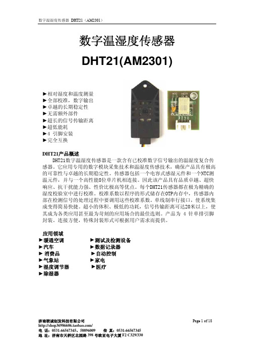
AM2301

温湿度模块AM2301 产品手册更多详情请登陆:一、产品概述AM2301湿敏电容数字温湿度模块是一款含有己校准数字信号输出的温湿度复合传感器。
它应用专用的数字模块采集技术和温湿度传感技术,确保产品具有极高的可靠性与卓越的长期稳定性。
传感器包括一个电容式感湿元件和一个高精度测温元件,并与一个高性能8位单片机相连接。
因此该产品具有品质卓越、超快响应、抗干扰能力强、性价比极高等优点。
每个传感器都在极为精确的湿度校验室中进行校准。
校准系数以程序的形式储存在单片机中,传感器内部在检测信号的处理过程中要调用这些校准系数。
标准单总线接口,使系统集成变得简易快捷。
超小的体积、极低的功耗,信号传输距离可达20米以上,使其成为各类应用甚至最为苛刻的应用场合的最佳选择。
产品为3引线(单总线接口)连接方便。
特殊封装形式可根据用户需求而提供。
实物图外形尺寸(单位:mm)二、应用范围暖通空调、除湿器、测试及检测设备、消费品、汽车、自动控制、数据记录器、家电、湿度调节器、医疗、气象站、及其他相关湿度检测控制等。
三、产品亮点超低能耗、传输距离远、全部自动化校准、采用电容式湿敏元件、完全互换、标准数字单总线输出、卓越的长期稳定性、采用高精度测温元件。
四、单总线接口定义4.1 AM2301引脚分配表1:AM2301引脚分配图1:AM2301引脚分配图4.2 电源引脚(VDD GND)AM2301的供电电压范围为3.3V - 5.2V,建议供电电压为5V。
4.3 串行数据(SDA)SDA引脚为三态结构,用于读、写传感器数据。
具体的通信时序,见通信协议的详细说明。
五、传感器性能 5.1 相对湿度表2: AM2301相对湿度性能表图2: 25℃时AM2301的相对湿度最大误差 图3:温度传感器的温度最大误差六、电气特性电气特性,如能耗,高、低电平,输入、输出电压等,都取决于电源。
表4详细说明了AM2301的电气特性,若没有标明,则表示供电电压为5V 。
AP2301GN中文资料
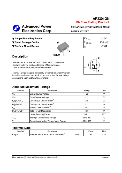
Advanced Power P-CHANNEL ENHANCEMENT MODE Electronics Corp.POWER MOSFET▼Simple Drive Requirement BV DSS-20V▼Small Package Outline R DS(ON)130mΩ▼Surface Mount Device I D- 2.6ADescriptionAbsolute Maximum RatingsSymbol UnitsV DS VV GS VI D@T A=25℃AI D@T A=70℃AI DM AP D@T A=25℃WW/℃T STG℃T J℃Symbol Value Unit Rthj-a Thermal Resistance Junction-ambient3Max.90℃/WData and specifications subject to change without noticeParameterDrain-Source VoltageGate-Source VoltageContinuous Drain Current3-55 to 150Linear Derating Factor1.38-55 to 150Thermal DataParameterTotal Power DissipationOperating Junction Temperature RangeStorage Temperature RangeContinuous Drain Current3-2.1Pulsed Drain Current1,2-10200407043AP2301GNRating- 20± 12-2.60.01Pb Free Plating ProductThe Advanced Power MOSFETs from APEC provide thedesigner with the best combination of fast switching,, low on-resistance and cost-effectiveness.The SOT-23 package is universally preferred for all commercial-industrial surface mount applications and suited for low voltageapplications such as DC/DC converters.DGSSOT-23AP2301GNElectrical Characteristics@T j=25o C(unless otherwise specified) Symbol Parameter Test Conditions Min.Typ.Max.Units BV DSS Drain-Source Breakdown Voltage V GS=0V, I D=-250uA-20--V ΔB V DSS/ΔT j Breakdown Voltage Temperature Coefficient Reference to 25℃, I D=-1mA--0.1-V/℃R DS(ON)Static Drain-Source On-Resistance2V GS=-5V, I D=-2.8A--130mΩV GS=-2.8V, I D=-2.0A--190mΩV GS(th)Gate Threshold Voltage V DS=V GS, I D=-250uA-0.5--V g fs Forward Transconductance V DS=-5V, I D=-2.8A- 4.4-S I DSS Drain-Source Leakage Current (Tj=25o C)V DS=-20V, V GS=0V---1uA Drain-Source Leakage Current (T j=70o C)V DS=-16V, V GS=0V---10uAI GSS Gate-Source Leakage VGS=±12V--nA Q g Total Gate Charge2I D=-2.8A- 5.210nC Q gs Gate-Source Charge V DS=-6V- 1.36-nC Q gd Gate-Drain ("Miller") Charge V GS=-5V-0.6-nC t d(on)Turn-on Delay Time2V DS=-15V- 5.2-ns t r Rise Time I D=-1A-9.7-ns t d(off)Turn-off Delay Time R G=6Ω,V GS=-10V-19-ns t f Fall Time R D=15Ω-29-ns C iss Input Capacitance V GS=0V-295-pF C oss Output Capacitance V DS=-6V-170-pF C rss Reverse Transfer Capacitance f=1.0MHz-65-pF Source-Drain DiodeSymbol Parameter Test Conditions Min.Typ.Max.Units I S Continuous Source Current ( Body Diode )V D=V G=0V , V S=-1.2V---1A I SM Pulsed Source Current ( Body Diode )1---10A V SD Forward On Voltage2T j=25℃, I S=-1.6A, V GS=0V---1.2VNotes:1.Pulse width limited by Max. junction temperature.2.Pulse width <300us , duty cycle <2%.3.Surface mounted on 1 in2 copper pad of FR4 board ; 270℃/W when mounted on min. copper pad.±100Fig 1. Typical Output Characteristics Fig 2. Typical Output CharacteristicsFig 3. On-Resistance v.s. Gate Voltage Fig 4. Normalized On-ResistanceFig 5. Forward Characteristic ofFig 6. Gate Threshold Voltage v.s.Reverse DiodeJunction TemperatureAP2301GNFig 7. Gate Charge Characteristics Fig 8. Typical Capacitance CharacteristicsFig 9. Maximum Safe Operating Area Fig 10. Effective Transient Thermal ImpedanceFig 11. Switching Time Waveform Fig 12. Gate Charge Waveform。
ADP2300_2301_cn开关电源中文版
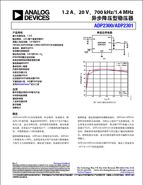
65 60
0 0.2 0.4 0.6 IOUT (A) 0.8
VIN = 12V VOUT = 5.0V 1.0 1.2
08342-069
图2. 功效与输出电流的关系
概述
ADP2300/ADP2301均为紧凑型、恒定频率、电流模式、降 压DC-DC调节器,集成功率MOSFET,采用3.0 V至20 V输入 电压工作,适合各种应用。这些器件内置精密、低压基准 电压源,非常适合产生最低为0.8 V、±2%精度的调节输出电 压,可提供最高1.2 A的负载电流。 提供两种频率选项: ADP2300工作频率为700 kHz,ADP2301 工作频率为1.4 MHz。这些选项允许用户在功效与整体解决 方案尺寸之间权衡取舍,做出适当选择。电流模式控制可 提供快速、稳定的线路和负载瞬态响应。 ADP2300/ ADP2301 器件均内置软启动功能,可防止上电时产生浪涌电流。其 它重要安全特性包括短路保护、热关断 (TSD)和输入欠压 闭锁 (UVLO)。 ADP2300/ADP2301具有精密使能引脚阈值 电压,因此很容易控制这些器件与其它输入/输出电源的时 序;利用电阻分压器,也可以将该器件用作可编程欠压闭 锁输入。 ADP2300/ADP2301采用6引脚TSOT封装,额定工作温度为 −40°C至+125°C的结温范围。
ADI中文版数据手册是英文版数据手册的译文,敬请谅解翻译中可能存在的语言组织或翻译错误,ADI不对翻译中存在的差异或由此产生的错误负责。如需确认任何词语的准确性,请参考ADI提供 的最新英文版数据手册。
ADP2300/ADP2301
目录
特性 ..............................................................................
2301导通电压
2301导通电压是一个重要的参数,它指的是在特定的温度和时间条件下,二极管或晶体管开始导电所需的最小电压。
这个参数对于理解二极管或晶体管的性能和限制非常重要。
首先,我们需要了解二极管或晶体管的工作原理。
这些电子设备基于半导体材料,如硅或锗。
当电流通过半导体时,它会形成电子-空穴对。
这些电子可以移动到电极的另一侧,形成一个电流。
然而,在某些材料中,电流不会自然流动,需要一个额外的电压来启动它。
这个电压就是导通电压。
对于2301二极管或晶体管,其导通电压会因型号、材料、温度、时间和其他因素而异。
具体的导通电压值需要参考二极管或晶体管的规格书或数据表。
在一般情况下,二极管或晶体管的导通电压通常在几伏特到几十伏特之间。
这可能因二极管或晶体管的类型、设计和材料而有所不同。
此外,环境温度也会影响导通电压,因为温度会影响半导体材料的电导率。
为了降低导通电压,工程师们一直在努力改进二极管或晶体管的材料和设计。
例如,使用更低电阻的材料、优化二极管或晶体管的几何形状和结构,以及使用更先进的制造技术,都可能有助于降低导通电压。
至于实际应用中如何使用这个参数,我们建议根据二极管或晶体管的规格和数据表进行操作。
一旦确定了二极管或晶体管的导通电压,就可以将其视为一个重要的限制条件,以确保电路的安全和稳定性。
总的来说,2301导通电压是一个关键参数,它决定了二极管或晶体管何时开始导电并允许电流流动。
了解这个参数对于理解二极管或晶体管的性能和限制非常重要,并在实际应用中确保电路的安全和稳定性。
如有需要,建议查阅相关二极管或晶体管的规格书或数据表以获取更准确的信息。
WOODWARD_2301D中文版
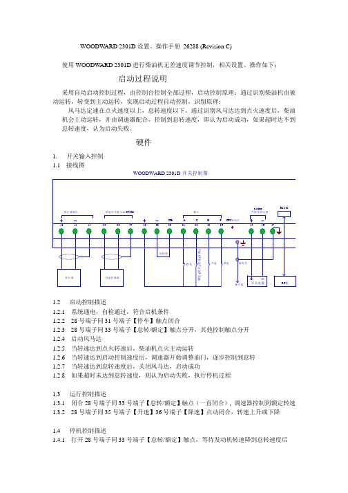
WOODW ARD 2301D设置、操作手册26288 (Revision C)使用WOODW ARD 2301D进行柴油机无差速度调节控制,相关设置、操作如下:启动过程说明采用自动启动控制过程,由控制台控制全部过程,启动控制原理:通过识别柴油机由被动运转,转变到主动运转,实现启动过程自动控制,识别原理:风马达定速在点火速度以上,怠转速度以下,通过识别风马达达到点火速度后,柴油机会主动运转,并由调速器配合,控制到怠转速度,即认为启动成功,如果超时达不到怠转速度,认为启动失败。
硬件1. 开关输入控制1.1接线图WOODWARD 2301D 开关控制图1.2 启动控制描述1.2.1 系统通电,自检通过,符合启机条件1.2.2 28号端子同31号端子【停车】触点闭合1.2.3 28号端子同33号端子【怠转/额定】触点分开,其他控制触点分开1.2.4 启动风马达1.2.5 当转速达到点火转速后,柴油机点火主动运转1.2.6 当转速达到启动控制速度后,调速器开始调整油门,逐步控制到怠转1.2.7 当转速达到怠转速度后,关闭风马达,启动成功1.2.8 如果超时未达到怠转速度,则认为启动失败,执行停机过程1.3 运行控制描述1.3.1 闭合28号端子同33号端子【怠转/额定】触点(一直闭合), 调速器控制到额定转速1.3.2 28号端子同35号端子【升速】36号端子【降速】点动闭合,转速上升或下降1.4 停机控制描述1.4.1 打开28号端子同33号端子【怠转/额定】触点,等待发动机转速降到怠转速度后1.4.2 打开28号端子同31号端子【停车】触点,调速器控制到停车状态注意:不可将【停车】触点直接用于停车,因为可能在额定高转速下,直接切断油路,对发动机不利,所以必须在怠转低转速下,切断油路,使发动机熄火,达到停机目的。
不可将【停车】触点用于紧急停车,以防执行器被卡,达不到紧急停车目的。
注意:在不使用模拟线路控制时,应将模拟线路设置为不使用。
APM2301A中文资料

ANPEC reserves the right to make changes to improve reliability or manufacturability without notice, and advise customers to obtain the latest version of relevant information to verify before placing orders.Pin DescriptionOrdering and Marking InformationFeaturesApplicationsAbsolute Maximum Ratings (T A = 25°C unless otherwise noted)• -20V/-2.8A , R DS(ON)=72m Ω(typ.) @ V GS =-10VR DS(ON)=100m Ω(typ.) @ V GS =-4.5V• Super High Dense Cell Design for ExtremelyLow R DS(ON)• Reliable and Rugged • SOT-23 Package• Power Management in Notebook Computer ,Portable Equipment and Battery Powered Systems.* Surface Mounted on FR4 Board, t ≤ 10 sec.G DSTop View of SOT-23Notesa : Pulse test ; pulse width ≤300µs, duty cycle ≤ 2%b: Guaranteed by design, not subject to production testingAbsolute Maximum Ratings Cont. (T A = 25°C unless otherwise noted)Electrical Characteristics (T A = 25°C unless otherwise noted)2468100.0300.0450.0600.0750.0900.1050.1200.1350.150012345246810-50-2502550751001251500.000.250.500.751.001.251.500.00.5 1.0 1.5 2.0 2.50246810Typical Characteristics-I D -D r a i n C u r r e n t (A )Transfer Characteristics-V GS - Gate-to-Source Voltage (V)Threshold Voltage vs. Junction T emperatureTj - Junction T emperature (°C)-V G S (t h )-T h r e s h o l d V o l t a g e (V )(N o r m a l i z e d )R D S (O N )-O n -R e s i s t a n c e (Ω)On-Resistance vs. Drain Current-I D - Drain Current (A)Output Characteristics-I D -D r a i n C u r r e n t (A )-V DS - Drain-to-Source Voltage (V)369121505101520-50-25025507510012515012345678910Typical CharacteristicsR D S (O N )-O n -R e s i s t a n c e (Ω)(N o r m a l i z e d )On-Resistance vs. Junction TemperatureT J - Junction Temperature (°C)-V DS - Drain-to-Source Voltage (V)CapacitanceC a p a c i t a n c e (p F )-V GS - Gate-to-Source Voltage (V)R D S (O N )-O n -R e s i s t a n c e (Ω)On-Resistance vs. Gate-to-Source VoltageGate ChargeQ G - Gate Charge (nC)-V G S -G a t e -S o u r c e V o l t a g e (V )0.00.20.40.60.8 1.0 1.2 1.4 1.61100.010.1110100024681012141E-41E-30.010.11101000.010.11Typical CharacteristicsP o w e r (W )Single Pulse PowerTime (sec)Square Wave Pulse Duration (sec)Source-Drain Diode Forward Voltage-I S -S o u r c e C u r r e n t (A )-V SD -Source-to-Drain Voltage (V)N o r m a l i z e d E f f e c t i v e T r a n s i e n t T h e r m a l I m p e d a n c eNormalized Thermal Transient Impedence, Junction to AmbientPackaging Information SOT-23Physical SpecificationsReflow Condition (IR/Convection or VPR Reflow)Reference JEDEC Standard J-STD-020A APRIL 1999Classification Reflow ProfilesPackage Reflow ConditionsPre-heat temperature183 CPeak temperatureTime°t e m p e r a t u r eReliability test programCarrier Tape & Reel DimensionsCover Tape DimensionsCustomer ServiceAnpec Electronics Corp.Head Office :5F, No. 2 Li-Hsin Road, SBIP,Hsin-Chu, T aiwan, R.O.C.T el : 886-3-5642000Fax : 886-3-5642050Taipei Branch :7F, No. 137, Lane 235, Pac Chiao Rd.,Hsin Tien City, Taipei Hsien, T aiwan, R. O. C.T el : 886-2-89191368Fax : 886-2-89191369。
WOODWARD 2301D设置、操作手册

WOODWARD 2301D设置、操作手册26288 (Revision C)使用WOODW ARD 2301D进行柴油机无差速度调节控制,相关设置、操作如下:启动过程说明采用自动启动控制过程,由控制台控制全部过程,启动控制原理:通过识别柴油机由被动运转,转变到主动运转,实现启动过程自动控制,识别原理:风马达定速在点火速度以上,怠转速度以下,通过识别风马达达到点火速度后,柴油机会主动运转,并由调速器配合,控制到怠转速度,即认为启动成功,如果超时达不到怠转速度,认为启动失败。
硬件1. 开关输入控制1.1接线图WOODWARD 2301D 开关控制图1.2 启动控制描述1.2.1 系统通电,自检通过,符合启机条件1.2.2 28号端子同31号端子【停车】触点闭合1.2.3 28号端子同33号端子【怠转/额定】触点分开,其他控制触点分开1.2.4 启动风马达1.2.5 当转速达到点火转速后,柴油机点火主动运转1.2.6 当转速达到启动控制速度后,调速器开始调整油门,逐步控制到怠转1.2.7 当转速达到怠转速度后,关闭风马达,启动成功1.2.8 如果超时未达到怠转速度,则认为启动失败,执行停机过程1.3 运行控制描述1.3.1 闭合28号端子同33号端子【怠转/额定】触点(一直闭合), 调速器控制到额定转速1.3.2 28号端子同35号端子【升速】36号端子【降速】点动闭合,转速上升或下降1.4 停机控制描述1.4.1 打开28号端子同33号端子【怠转/额定】触点,等待发动机转速降到怠转速度后1.4.2 打开28号端子同31号端子【停车】触点,调速器控制到停车状态注意:不可将【停车】触点直接用于停车,因为可能在额定高转速下,直接切断油路,对发动机不利,所以必须在怠转低转速下,切断油路,使发动机熄火,达到停机目的。
不可将【停车】触点用于紧急停车,以防执行器被卡,达不到紧急停车目的。
注意:在不使用模拟线路控制时,应将模拟线路设置为不使用。
2301A整定参数
) 2301A面板上的电位器的初始整定a.额定转速电位器(Rated speed),将发电机组控制柜门上的速度给定电位器R1调至中间位置(5圈),将额定转速电位器调至最小位置,待柴油机升速后,调它使柴油机到达额定转速1500rpm,顺时针旋转为转速升高。
b.怠速电位器(Low Idle Speed),设置至最大位置,顺时针方向为升高怠速值。
c.初始燃油限制电位器(Start Fuel Limit),置于最大位置,顺时针方向为增大初始值。
d.升速时间电位器(Ramp Time),使其在最小位置,顺时针为时间加长。
e.增益电位器(Gain)和稳定性电位器(Reset),置于中间位置。
快速性电位器(Actuator Compensation)放在0~2范围内的刻度上,顺时针方向为增强性能。
f.负荷增益电位器(Load Gain),置于中间位置,顺时针方向增大负载输出信号。
g.调差电位器(Droop),处于最小位置,顺时针方向增大调差。
(3) 转速稳定工作调整a.若柴油机快速振荡,应逆时针慢慢减小增益(Gain)电位器,直到稳定为止。
b.若柴油机慢速游荡,应顺时针增加稳定性(Reset)直到稳定为止。
如果调大稳定性电位器不能改善柴油机的稳定,则还需慢慢调小增益电位器或增益和快速性(Actuator Compensation)电位器都慢慢调小。
c.小范围的慢速不稳应顺时针增大快速性(Actuator Compensation) 电位器,小范围的快速不稳应逆时针调小快速性电位器。
(4) 转速动态调整a.调整增益和稳定性电位器,使转速变化获得最佳动态响应。
b.用高灵敏电压表监视20#(A+)和21#(B-)为执行器输出的直流电压。
c.调大增益电位器,可使突变负载时提供转速变化的快速传输响应,应慢慢顺时针增大增益电位器,直至监视20#、21#上的电压表现出轻微不稳,然后轻微逆时针调小一点增益电位器,使监视表上的电压稳定可读。
WOODWARD_2301D中文版

WOODW ARD 2301D设置、操作手册26288 (Revision C)使用WOODW ARD 2301D进行柴油机无差速度调节控制,相关设置、操作如下:启动过程说明采用自动启动控制过程,由控制台控制全部过程,启动控制原理:通过识别柴油机由被动运转,转变到主动运转,实现启动过程自动控制,识别原理:风马达定速在点火速度以上,怠转速度以下,通过识别风马达达到点火速度后,柴油机会主动运转,并由调速器配合,控制到怠转速度,即认为启动成功,如果超时达不到怠转速度,认为启动失败。
硬件1. 开关输入控制1.1接线图WOODWARD 2301D 开关控制图1.2 启动控制描述1.2.1 系统通电,自检通过,符合启机条件1.2.2 28号端子同31号端子【停车】触点闭合1.2.3 28号端子同33号端子【怠转/额定】触点分开,其他控制触点分开1.2.4 启动风马达1.2.5 当转速达到点火转速后,柴油机点火主动运转1.2.6 当转速达到启动控制速度后,调速器开始调整油门,逐步控制到怠转1.2.7 当转速达到怠转速度后,关闭风马达,启动成功1.2.8 如果超时未达到怠转速度,则认为启动失败,执行停机过程1.3 运行控制描述1.3.1 闭合28号端子同33号端子【怠转/额定】触点(一直闭合), 调速器控制到额定转速1.3.2 28号端子同35号端子【升速】36号端子【降速】点动闭合,转速上升或下降1.4 停机控制描述1.4.1 打开28号端子同33号端子【怠转/额定】触点,等待发动机转速降到怠转速度后1.4.2 打开28号端子同31号端子【停车】触点,调速器控制到停车状态注意:不可将【停车】触点直接用于停车,因为可能在额定高转速下,直接切断油路,对发动机不利,所以必须在怠转低转速下,切断油路,使发动机熄火,达到停机目的。
不可将【停车】触点用于紧急停车,以防执行器被卡,达不到紧急停车目的。
注意:在不使用模拟线路控制时,应将模拟线路设置为不使用。
AF2301P中文资料
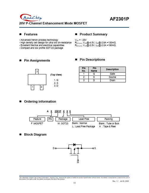
AF2301P20V P-Channel Enhancement Mode MOSFETFeatures- Advanced trench process technology- High density cell design for ultra low on-resistance - Excellent thermal and electrical capabilities - Compact and low profile SOT-23 packagePin Assignments321(Top View)1. G2. S3. DProduct SummaryV DS = - 20VR DS (on), V GS @-4.5V, I DS @-2.8A =130m Ω. R DS (on), V GS @-2.5V, I DS @-2.0A =190m Ω.Pin DescriptionsPin No. Pin NameDescription 1 GGate 2 SSource 3 DDrainOrdering informationF :MOSFETW: SOT23Blank : NormalL : Lead Free PackageBlank : Tube or Bulk A : Tape & ReelBlock DiagramSDAF2301P20V P-Channel Enhancement Mode MOSFETAbsolute Maximum Ratings (T A =25ºC unless otherwise noted)Symbol Parameter Rating Units V DS Drain-Source Voltage -20 VV GS Gate-Source Voltage ±8 V I D Continuous Drain Current -2.3 AI DM Pulsed Drain Current -10 A T A =25ºC 1.25 P D Maximum Power Dissipation T A =70ºC 0.8 W T J Operating Junction Temperature +150 ºC T J , T STG Operating Junction and Storage Temperature Range -55 to +150 ºCThermal PerformanceSymbol ParameterLimit Units T L Lead Temperature (1/8” from case)5 S R θJA Junction to Ambient Thermal Resistance (PCB mounted) 100 ºC/WNote: Surface mounted on FR4 board t < 5 sec.Electrical Characteristics Rate I D =-2.3A, (T A =25o C unless otherwise noted)LimitsSymbol Parameter Test ConditionsMin.Typ. Max.UnitStaticBV DSS Drain-Source Breakdown Voltage V GS =0V, I D =-250uA -20 - - VV GS =-4.5V, I D =-2.8A - 95 130R DS(ON) Drain-Source On-State Resistance V GS =-2.5V, I D =-2.0A - 122 190m ΩV GS(TH) Gate Threshold Voltage V DS = V GS , I D =-250uA -0.45- - V I DSS Zero Gate Voltage Drain Current V DS =-16V, V GS =0V - - -1.0 uA I GSS Gate Body Leakage V GS =±8V, V DS =0V - - ±100nA I D(ON) On-State Drain Current V DS =-5V, V GS =-10V -6 - - A g fs Forward Tranconductance V DS =-5V, I D =-2.8A - 6.5 - S DynamicQ g Total Gate Charge - 5.4 10Q gs Gate-Source Charge - 0.8 - Q gd Gate-Drain Charge V DS =-6V, I D =-2.8A,V GS =-4.5V- 1.1 - nCt d(on) Turn-On Delay Time - 5 25t r Turn-On Rise Time - 19 60t d(off) Turn-Off Delay Time - 95 110 t f Turn-Off Fall-Time V DD =-6V, R L =6Ω,I D =-1A, V GEN =-4.5V,R G =6Ω - 65 80 nS C iss Input Capacitance - 447 -C oss Output Capacitance - 127 - C rss Reverse Transfer CapacitanceV DS =-6V, V GS =0V,f=1.0MHz- 80 - pFSource-Drain DiodeI S Max. Diode Forward Current - - -1.6 A V SD Diode Forward Voltage I S =-1.6A, V GS =0V - -0.8 -1.2 VNote: Pulse test: pulse width < 300uS, duty cycle < 2%20V P-Channel Enhancement Mode MOSFET Marking InformationAppendixPart Number Package Device CodeAF2301P SOT23-301Switching Test CircuitVVGSOUTSwitching WaveformsOutput, VInput, VIN20V P-Channel Enhancement Mode MOSFETPackage InformationLDimensions In Millimeters Dimensions In InchesSymbolMin. Nom. Max. Min. Nom. Max.0.0550.0390.0471.401.20A 1.000.000 - 0.004A1 0.00 - 0.100.0510.045A2 1.00 1.15 1.300.0390.014 - 0.020b 0.35 - 0.50C 0.10 0.175 0.25 0.004 0.007 0.0100.1140.1060.122D 2.703.102.900.0710.0630.055E 1.401.601.800.0790.0910.0672.002.30e 1.700.1060.1180.094HE 2.40 2.70 3.000.012 - 0.022L 0.30 - 0.55。
安迪尔 CN2300 系列

P1⁄4 DIN Ramp/SoakController with Graphics and USB InterfaceU G raphical LCD Text Display (Red/Green)U F ront Mounted USB Interface PortU 64 Independent ProgramsU 255 Segments per ProgramU U niversal InputsU A utotuneU M odular Isolated Control OutputsU D ata Logging Models (Data, Alarms and Events)U R S485 Communications (Optional)U S oftware with Configuration Cable (Optional)U A larm FunctionsU 5 Language Options (English, French, German, Italian, Spanish)The CN2300 Series ¼ DIN profile controller with graphic/text LCD display and USB interface is an affordable temperature and process controller with advanced functionality including datalogging options. Designed to improve user efficiency many features are integrated to reduce commissioning time, simplify operation and minimize maintenance downtime.Features include graphic easy to read backlit LCD display, dual color screen (green/red), multi-language option, custom splash-screen on startup (bitmap file), alarm status view, on screen trend view, LEDs to indicate heat, cool, autotuning and alarm.Easy setup wizard via front keys for quick configuration of inputs, alarms, outputs, communications and real-time clock. Universal input for thermocouple, RTD’s and linear DC process signals (mA, mV or V). Flexible modular output options include mechanical relay, dc Pulse, AC SSR triac and linear outputs. Select to precisely match the process, digital input (2 max) for setpoint selection, profile control, datalogging start/stop, control output enable/disable or auto/manual control. The CN2300 series features configurable menus (using optional software with cable for configurating units via RJ11 configuration socket), USB port for local upload/download of configuration files and download logged data to or from a USB memory stick. This allows easy configuration of multiple instruments by copying from one unit to another.Profile feature includes 255 segments to allocate freely in up to 64 programs. Programs include ramp, soak, hold, loop or jump to other profile. User defined text profile name, delayed or real-time day/time profile start, and up to 5 event outputs.The CN2300 data logging models include historic process data for analysis or reporting, and export data files via front USB or optional communications, and will log process values, setpoints or alarms (including minimum, maximum and average), with logging intervals from 1s to 30m. Many options include analog remote setpoint, built in 24 Vdc transmitter power supply, and graphical software.Dual color, graphical LCD text display changes color from green to red.CN2301-R1-R2-R3 shown smaller than actual size.Front USB port.P*Linearization better than ±0.2 C (±0.05 typical). Linearization for other ranges is better than better than 0.5 C. Optional decimal place can be displayed up to 999.9°C/F 0 to 3 places, but limited to 5 display digits (e.g 9999.9).Supported RTD Types and Ranges: 3-wire, PT100: -199 to 800°C (-328 to 1472°F)NI120: -80 to 240°C (-112 to 464°F) Optional decimal place can be displayed up to 999.9°C/F RTD Excitation: Sensor current 150μA ±10%Lead Resistance: <0.5% of span error for max 50 Ωper lead, balanced Process InputSampling Rate: 10 per secondResolution: 16 bits, always four times better than display resolutionImpedance: >10M Ω resistive, except DC mA (5 Ω) and V (47k Ω)Temperature Stability: Error <0.01% of span per °C change inambient temperature Supply Variation: Supply voltage influence negligible withinsupply limits Humidity Influence: Negligible if non-condensingProcess Display: Displays up to 5% over and5% under span limits Process Variable Input Offset: Reading adjustable± Controller Span. +ve values added to Process Variable, -ve values subtracted from Process VariableSensor Break Detection: T hermocouple and RTD: Control goes to pre-set power value High and Sensor Break: Alarms activate Linear (4 to 20 mA, 2 to 10V and 1 to 5V only): Control goes to pre-set power value Low and Sensor Break: Alarms activateIsolation: Isolated from all outputs (except SSR driver) at 240 Vac DC Calibration: ±0.1% of full range, ±1LSD DC Input Multi-Point Linearization:Up to 15 scaling values can be defined anywhere between 0.1 and 100% of input Accuracy: ±0.25% of input range 1 LSD Sampling Rate: 4 per secondResolution: 16 bitsImpedance:>10M resistive, except DC mA (10 Ω) andV (47k Ω)Sensor Break Detection:4 to 20mA, 2 to 10V and 1 to 5Vranges only. Control goes to pre-set power value if Aux input is the active setpoint sourceIsolation:Reinforced safety isolation from outputs and inputs (except to digital Input B)Auxiliary Input Scaling:Scalable as remote setpoint (RSP) input between -1999 and 9999, constrained within setpoint limits Digital InputsVolt-Free Contacts (or TTL):Open contacts (>5000 or 2 to 24 Vdc signal = Logic High Closed contacts) (<50 or -0.6 to +0.8 Vdc signal = Logic Low)Isolation:Reinforced safety isolation from inputs and other outputs Digital Input Sensitivity:Edge sensitive; requires high-lowor low-high transition to change function; response within <0.25 secondCN2301-R1-R2-R3shown smaller than actual size.POutputsIsolation: Reinforced safety isolation from inputs andother outputs (common specification for all output types)Single Relay:T ype and Rating: Single pole single throw (SPST), 2A resistive at 120/240 Vac Lifetime: >500,000 operations at rated voltage/current Dual Relay: T ype and Rating: Single pole single throw (SPST), 2A resistive at 120/240 Vac (dual relay modules have shared common) Lifetime: >200,000 operations at rated voltage/current Quad Relay: T ype and Rating: Single pole single throw (SPST), 2A resistive at 120/240 Vac (dual relay modules have shared common) Lifetime: >500,000 operations at rated voltage/current DC Pulse:D rive Capability: SSR driver voltage >10V into 500 Ω minimum Triac: Operating Voltage: 20 to 280Vrms (47 to 63Hz)C urrent Rating: 0.01 to 1A (full cycle rms on-state @ 25°C); de-rates linearly above 40°C to 0.5A @ 80°C Linear DC:R anges: 0 to 5V , 0 to 10V , 1 to 5V , 2 to 10V and0 to 20 mA, 4 to 20 mA (selectable) with 2% over/ under-drive whenused for control outputsR esolution: 8 bits in 250 mS (10 bits in 1s typical,>10 bits in >1s typical)A ccuracy: ±0.25% of range, (mA @ 250, V @ 2k)Degrades linearly to ±0.5% for increasing burden (to specification limits)Transmitter PSU Power Rating: 24 V nominal (19 to 28 Vdc) into910 Ω minimum resistance (option to use DC Linearoutput as 0 to 10V stabilised PSU)Isolation: Reinforced safety isolation from inputs and other outputsCommunicationsPC ConfigurationC onnection: RS232 via PC configurator cable to RJ11 socket under case I solation: Not isolated from input or SSR driver outputs;for bench configuration only RS485C onnection: Locates in option alot A; connection via rear terminals Protocol: MODBUS RTU S lave/Master Mode: Slave address range 1 to 255 or setpoint master mode S upported Speeds: 4800, 9600, 19200, 38400, 57600 or 115200 bps D ata Type: 8 data bits and 1 stop bit; odd, even or no parity I solation: 240V reinforced safety isolation from all inputs and outputs Ethernet C onnection: Locates in option slot A, connection via RJ45 connector on top of case Protocol: MODBUS TCP (slave only) Supported Speed: 10BaseT or 100BaseT I solation: 240V reinforced safety isolation from the supply, inputs and outputs (except SSR drivers)Loop ControlTuning Types:Pre-tune, auto pre-tune, self-tune or manual tuning Proportional Bands:Primary and secondary (e.g. heat and cool) 0.5% to 999.9% of input span in 0.1% increments, or on/off controlAutomatic Reset:Integral time constant, 1 second to 99 minutes 59 seconds and off Rate:Derivative time constant, 1 second to 99 minutes 59 seconds and off Manual Reset:Bias 0 to 100% (-100% to +100% primary and secondary)Deadband/ Overlap:-20% to +20% of primary + secondary proportional band ON/OFF Differential: 0.1% to 10.0% of input span Auto/Manual Control:Selectable with “bumpless” transfer when switching between automatic and manual control Cycle Times: Selectable from 0.5s to 512s Setpoint Ramp:Ramp rate selectable 1 to 9999 LSDs per hour and infinite AlarmsAlarm Types:Up to 5 alarms selectable as process high,process low, band, deviation, rate of signal change (per minute), sensor/input break, loop alarm; band and deviation(high or low) alarm values are relative to the current setpoint valueAlarm Hysteresis:A deadband from 1 LSD to full span (in display units) for process, band or deviation alarms; rate of change alarm hysteresis is the shortest time (1 to 9999 seconds) the rate of change must be above the threshold for the alarm activate, or fall below the threshold to deactivate Note: If the duration is less than this time, the alarm will not activate no matter how fast the rate of rise.Combination AlarmOutputs:Logical OR of alarms 1 and 2, 1 to 3, 1 to 4 or 1 to 5. Logical AND of alarms 1 to 5 with Profiler Events 1 to 5Operating Conditions (for Indoor Use)Temperature: Operating:0 to 55°C (0 to 131°F) Storage: -20 to 80°C (-4 to 176°F)Relative Humidity:20 to 95% non-condensingEasy programming via graphical menu display.PSupply Voltage and Power: Mains Versions: 100 to 240 Vac ±10%, 50/60 Hz, 20VA L ow Voltage Versions: 20 to 48VC 50/60 Hz 15VA or 22 to 65 Vdc 12 W Environmental Front Panel Sealing: T o IP66 (IP65 front USB connector)IP20 behind the panel Display Display Type: 160 x 80 pixel, monochrome graphic LCD with a dual colour (red/green) backlight Display Area: 66.54 W x 37.42 mm H (2.62 x 1.65")Display Characters: 0 to 9, a to z, A to Z, plus ( ) - and _Trend View: 120 of 240 data points shown in a scrollable window; data is not retained when power turned off or if time base is changed Trend Data: Any active alarm plus PV (solid) and SP (dotted) at sample time or maximum/minimum PV between samples (candle-stick graph)Trend Sample Rate: 1; 2; 5; 10; 15; 30 seconds or 1; 2; 5; 10; 15; 30 minutes Additional Communications Options–USB*Connection: Locates in option slot C; connection via front mounted connector Protocol: USB 1.1 or 2.0 compatible; mass storage class Supply Current: Up to 250 mA Targeted Peripheral: USB memory stick Isolation: Reinforced safety isolation from all inputs and outputs *Not used for PC configuration.Data RecorderRecording Memory: 1Mb non-volatile flash memory;data retained when power is turned off Recording Interval: 1; 2; 5; 10; 15; 30 seconds or 1; 2; 5; 10;15; 30 minutes Recording Capacity: Dependant on sample rate andnumber of values recorded; two values can be recorded for up to 7 days at 10s intervals; more values or faster sample rates reduce the maximum durationRTC Battery Type: CR 1616 3V lithium; clock runs for >1year without power RTC Accuracy: Real time clock error <1second per dayProfilerProfile Limits: Number of profiles: 64 maximum T otal Number of Segments (All Programs): 255 maximumLoop Back: 1 to 9999 loops back to specified segmentProfile Cycling: 1 to 9999 or Infinite repeats per profileSequence Repeats: 1 to 9999 or Infinite repeats of joinedprofile sequences Segment Types: Ramp up/down over time, ramp rate up/down, step, dwell, hold, join a profile, end or repeat sequence then endTimebase: hh:mm:ss (hours, minutes and seconds)Segment Time:Maximum segment time 99:59:59 hh:mm:ss;Use loop-back for longer segments (e.g. 24:00:00 x 100 loops = 100 days)Ramp Rate: 0.001 to 9999.9 display units per hour Hold Segment Release:Release with key press, at time of day or digital input Start From:First segment starts from current setpoint or current input value Delayed Start:After 0 to 99:59 (hh:mm) delay, or at specified day(s) and time Abort Action: Keep last profile setpoint, use controller setpoint or control outputs off Power/Signal Loss Recovery: Continue profile, restart profile, keep last profile setpoint, use controller setpoint or control outputs offAuto-Hold:Hold if input >band above and/or below SP for each segment Profile Control:Run, manual hold/release, abort or jump to next segment Segment Events:Events turn on for the duration of the segment; for end segments, the event state persists until another profile starts, the user exits from profiler mode, or the unit is powered downDimensionsFront Bezel Size: 1⁄4 DIN; 96 x 96 mm (3.78 x 3.78")Mounting: Plug-in with panel mounting fixing strap Panel Cut-Out Size:92 x 92 mm (3.62 x 3.62") (maximum panel thickness 6.0 mm [0.236"])Depth Behind Panel: 117 mm (4.61")Ventilation:20 mm (0.787") gap required above, below and behind Weight: 0.65 kg (1.43 lb) maximum Terminals:Screw type (combination head)Easy ramp and soak programming via graphical menu.POrdering Examples: CN2301-R1-R2-R3, profile controller with3 relay outputs, front USB interface, and operator’s manual.OCW-2, OMEGACARE SM extends standard 3-year warranty to a totalof 5 years.CN2301-F1-R2-R3-LV, profile controller with 1 analog and 2 relay outputs, low voltage, front USB interface, and operator’s manual.OCW-2, OMEGACARE SMextends standard 3-year warranty to a totalof 5 years.。
AM2301(DHT21)规格书
引线定义(三
2
黄线
DATA
3
黑线
GND
4
NC
注释 供电 3.3-5.5VDC 串行数据,单总线 接地,电源负极 空脚,请悬空(不要接Vcc或Gnd)
济南联诚创发科技有限公司
/ 电 话:0531-66567345、58896009 传 真:0531-66567345 地 址:济南市天桥区北园路 398 号欧亚电子大厦 F2 C329/330
;公司 ; **********
;*********************************************;
;--------------------
;----变量定义区------
;--------------------
FLAG
EQU 30H
U8comdata EQU 31H
U8T_data_H EQU 32H
;允许串口中断
SETB EA
;允许全部外设中断
MAIN:
;--------------------------;-----调用湿度读取子程序---;---------------------------
LCALL RH
济南联诚创发科技有限公司 / 电 话:0531-66567345、58896009 传 真:0531-66567345 地 址:济南市天桥区北园路 398 号欧亚电子大厦 F2 C329/330
图1 空闲时总线为高电平,通讯开始时主机(MCU)拉低总线500us后释放总线,延时 20-40us后主机开始检测从机(DHT21)的响应信号。 从机的响应信号是一个80us左右的低电平,随后从机在拉高总线80us左右代表即 将进入数据传送。
- 1、下载文档前请自行甄别文档内容的完整性,平台不提供额外的编辑、内容补充、找答案等附加服务。
- 2、"仅部分预览"的文档,不可在线预览部分如存在完整性等问题,可反馈申请退款(可完整预览的文档不适用该条件!)。
- 3、如文档侵犯您的权益,请联系客服反馈,我们会尽快为您处理(人工客服工作时间:9:00-18:30)。
MMA2301D Rev 4, 03/2006Freescale Semiconductor Technical Data© Freescale Semiconductor, Inc., 2006. All rights reserved.Surface MountMicromachined AccelerometerThe MMA series of silicon capacitive, micromachined accelerometers feature signal conditioning, a 4-pole low pass filter and temperature compensation.Zero-g offset full scale span and filter cut-off are factory set and require no external devices. A full system self-test capability verifies system functionality.Features •Integral Signal Conditioning •Linear Output•Ratiometric Performance•4th Order Bessel Filter Preserves Pulse Shape Integrity •Calibrated Self-test•Low Voltage Detect, Clock Monitor, and EPROM Parity Check Status •Transducer Hermetically Sealed at Wafer Level for Superior Reliability •Robust Design, High Shocks SurvivabilityTypical Applications •Vibration Monitoring and Recording •Impact MonitoringORDERING INFORMATIONDevice Name Temperature Range Case No.Package MMA2301D –40° to 125°C 475-01SOIC-16MMA2301DR2 –40° to 125°C 475-01SOIC16, Tape & ReelMMA2301EG –40° to 125°C 475-01SOIC-16MMA2301EGR2–40° to 125°C475-01SOIC16, Tape & ReelMMA2301MMA2301D: X-AXIS SENSITIVITYMICROMACHINED ACCELEROMETER±200GG-Cell SensorIntegratorGainFilterTempS elf-TestControl Logic and EPROM Trim CircuitsClock GeneratorOscillatorV DDV OUTV SSSTSTATUSFigure 1. Simplified Accelerometer Functional Block Diagram N/C N/C N/C ST V OUT STATUSV SSV DDN/C N/C N/C N/C N/C N/C N/C N/C12345678161514131211109Figure 2. Pin ConnectionsMMA2301D ELECTRO STATIC DISCHARGE (ESD)WARNING:This device is sensitive to electrostatic discharge.Although the accelerometers contain internal 2kV ESD protection circuitry, extra precaution must be taken by the user to protect the chip from ESD. A charge of over 2000 volts can accumulate on the human body or associated test equipment. A charge of this magnitude can alter the performance or cause failure of the chip. When handling the accelerometer, proper ESD precautions should be followed to avoid exposing the device to discharges which may be detrimental to its performance.Table1. Maximum Ratings(Maximum ratings are the limits to which the device can be exposed without causing permanent damage.)Rating Symbol Value Unit Powered Acceleration (all axes)G pd1500g Unpowered Acceleration (all axes)G upd2000g Supply Voltage V DD–0.3 to +7.0VDrop Test(1)1.Dropped onto concrete surface from any axis.D drop 1.2mStorage Temperature Range T stg–40 to +125°CSensorsSensorsMMA2301DTable 2. Operating Characteristics(Unless otherwise noted: -40°C ≤ T A ≤ +105°C, 4.75 ≤ VDD ≤ 5.25, Acceleration = 0g, Loaded output)(1)1.For a loaded output the measurements are observed after an RC filter consisting of a 1 k Ω resistor and a 0.01 µF capacitor to ground.CharacteristicSymbol Min Typ Max Unit Operating Range (2)Supply Voltage (3)Supply CurrentOperating Temperature Range Acceleration Range 2.These limits define the range of operation for which the part will meet specification.3.Within the supply range of4.75 and5.25 volts, the device operates as a fully calibrated linear accelerometer. Beyond these supply limits the device may operate as a linear device but is not guaranteed to be in calibration.V DD I DD T A g FS 4.753.0-40— 5.0——225 5.256.0+125—V mA °C g Output SignalZero g (T A = 25°C, V DD = 5.0 V)(4)Zero gSensitivity (T A = 25°C, V DD = 5.0 V)(5)SensitivityBandwidth Response Nonlinearity 4.The device can measure both + and - acceleration. With no input acceleration the output is at midsupply. For positive acceleration the output will increase above V DD /2 and for negative acceleration the output will decrease below V DD /2.5.The device is calibrated at 35g.V OFF V OFF,V S S V f -3dB NL OUT 2.40.46 V DD9.51.86360-1.02.50.50 V DD 10.02.0400— 2.60.54 V DD 10.52.144401.0V V mV/g mV/g/V Hz % FSO NoiseRMS (.01-1 kHz)Power Spectral DensityClock Noise (without RC load on output)(6)6.At clock frequency ≅ 70 kHz.n RMS n PSD n CLK ————1102.0 2.8——mVrms µV/(Hz 1/2)mVpkSelf-TestOutput Response Input Low Input HighInput Loading (7)Response Time (8)7.The digital input pin has an internal pull-down current source to prevent inadvertent self test initiation due to external board level leakages.8.Time for the output to reach 90% of its final value after a self-test is initiated.g ST V IL V IH I IN t ST 24V SS 0.7 x V DD-30—30——-1002.0360.3 x V DDV DD -26010g V V µA ms Status (9) (10)Output Low (I load = 100 µA)Output High (I load = 100 µA)9.The Status pin output is not valid following power-up until at least one rising edge has been applied to the self-test pin. The Status pin is high whenever the self-test input is high, as a means to check the connectivity of the self-test and Status pins in the application.10.The Status pin output latches high if a Low Voltage Detection or Clock Frequency failure occurs, or the EPROM parity changes to odd. TheStatus pin can be reset low if the self-test pin is pulsed with a high input for at least 100 us, unless a fault condition continues to exist.V OL V OH —V DD -0.8——0.4—V V Minimum Supply Voltage (LVD Trip)V LVD 2.7 3.25 4.0V Clock Monitor Fail Detection Frequency f min 50—260kHz Output Stage PerformanceElectrical Saturation Recovery Time (11)Full Scale Output Range (I OUT = 200 µA)Capacitive Load Drive (12)Output Impedance 11.Time for amplifiers to recover after an acceleration signal causing them to saturate.12.Preserves phase margin (60°) to guarantee output amplifier stability.t DELAY V FSO C L Z O —0.25——0.2——300—V DD -0.25100—ms V pF ΩMechanical Characteristics Transverse Sensitivity (13)Package Resonance13.A measure of the device's ability to reject an acceleration applied 90° from the true axis of sensitivity.V XZ,YZ f PKG———105.0—% FSO kHzMMA2301D PRINCIPLE OF OPERATIONThe Freescale Semiconductor, Inc. accelerometer is a surface-micromachined integrated-circuit accelerometer.The device consists of a surface micromachined capacitive sensing cell (g-cell) and a CMOS signal conditioning ASIC contained in a single integrated circuit package. The sensing element is sealed hermetically at the wafer level using a bulk micromachined cap wafer.The g-cell is a mechanical structure formed from semiconductor materials (polysilicon) using semiconductor processes (masking and etching). It can be modeled as a set of beams attached to a movable central mass that move between fixed beams. The movable beams can be deflected from their rest position by subjecting the system to an acceleration( Figure3).As the beams attached to the central mass move, the distance from them to the fixed beams on one side will increase by the same amount that the distance to the fixed beams on the other side decreases. The change in distance is a measure of acceleration.The g-cell plates form two back-to-back capacitors (Figure3). As the central mass moves with acceleration, the distance between the beams change and each capacitor's value will change, (C = NAε/D). Where A is the area of the facing side of the beam, ε is the dielectric constant, D is the distance between the beams, and N is the number of beams.The CMOS ASIC uses switched capacitor techniques to measure the g-cell capacitors and extract the acceleration data from the difference between the two capacitors. The ASIC also signal conditions and filters (switched capacitor) the signal, providing a high level output voltage that is ratiometric and proportional to acceleration.Figure3. Simplified Transducer Physical Model versusTransducer Physical ModelSPECIAL FEATURESFilteringThe accelerometers contain an onboard 4-pole switched capacitor filter. A Bessel implementation is used because it provides a maximally flat delay response (linear phase) thus preserving pulse shape integrity. Because the filter is realized using switched capacitor techniques, there is no requirement for external passive components (resistors and capacitors) to set the cut-off frequency.Self-TestThe sensor provides a self-test feature that allows the verification of the mechanical and electrical integrity of the accelerometer at any time before or after installation. This feature is critical in applications such as automotive airbag systems where system integrity must be ensured over the life of the vehicle. A fourth plate is used in the g-cell as a self-test plate. When the user applies a logic high input to the self-test pin, a calibrated potential is applied across the self-test plate and the moveable plate. The resulting electrostatic force (Fe=1/2AV2/d2) causes the center plate to deflect. The resultant deflection is measured by the accelerometer's control ASIC and a proportional output voltage results. This procedure assures that both the mechanical (g-cell) and electronic sections of the accelerometer are functioning.RatiometricityRatiometricity simply means that the output offset voltage and sensitivity will scale linearly with applied supply voltage. That is, as you increase supply voltage the sensitivity and offset increase linearly; as supply voltage decreases, offset and sensitivity decrease linearly. This is a key feature when interfacing to a microcontroller or an A/D converter because it provides system level cancellation of supply induced errors in the analog to digital conversion process.StatusFreescale accelerometers include fault detection circuitry and a fault latch. The Status pin is an output from the fault latch, OR'd with self-test, and is set high whenever one (or more) of the following events occur:•Supply voltage falls below the Low Voltage Detect (LVD) voltage threshold•Clock oscillator falls below the clock monitor minimum frequency•Parity of the EPROM bits becomes odd in number.The fault latch can be reset by a rising edge on the self-test input pin, unless one (or more) of the fault conditions continues to exist.AccelerationSensorsSensorsMMA2301DBASIC CONNECTIONSPINOUT DESCRIPTIONFigure 4. SOIC Accelerometer with RecommendedConnection DiagramFigure 5. Recommend PCB Layout for InterfacingAccelerometer to Microcontroller NOTES:•Use a 0.1 µF capacitor on V DD to decouple the powersource.•Physical coupling distance of the accelerometer to themicrocontroller should be minimal.•Place a ground plane beneath the accelerometer toreduce noise, the ground plane should be attached to all of the open ended terminals shown in Figure 5•Use an RC filter of 1 k Ω and 0.01 µF on the output of theaccelerometer to minimize clock noise (from the switched capacitor filter circuit).•PCB layout of power and ground should not couple powersupply noise.•Accelerometer and microcontroller should not be a highcurrent path.A/D sampling rate and any external power supplyswitching frequency should be selected such that they do not interfere with the internal accelerometer sampling frequency. This will prevent aliasing errors.Table 3. Pin DescriptionsPin No.Pin Name Description1 thru 3N/C Leave unconnected.4ST Logic input pin used to initiate self-test.5V OUT Output voltage of the accelerometer.6STATUS Logic output pin to indicate fault.7V SS The power supply ground.8V DD The power supply input.9 thru 13Trim pinsUsed for factory trim. Leave unconnected.14 thru 16—No internal connection. Leave unconnected.101112131415169N/C N/C N/C N/C N/C N/C N/C N/C87654321N/C N/C N/C ST V OUT STATUSV DDV SS MMA2301DST V DDV SSV OUT Output SignalR11 k Ω5C20.01 µF487Logic InputV DDC10.1 µF6Status P0A/D InV RHV SSV DDST V OUT V SS V DD0.01 µF1 k Ω0.1 µFPower SupplyC0.1 µF P1STATUSM i c r o c o n t r o l l e rA c c e l e r o m e t e rC C C0.1 µF PCB Layout RMMA2301DSensorsSensorsMMA2301DMINIMUM RECOMMENDED FOOTPRINT FOR SURFACE MOUNTED APPLICATIONSSurface mount board layout is a critical portion of the total design. The footprint for the surface mount packages must be the correct size to ensure proper solder connection interface between the board and the package. With thecorrect footprint, the packages will self-align when subjected to a solder reflow process. It is always recommended to design boards with a solder mask layer to avoid bridging and shorting between solder pads.Figure 6. Footprint SOIC-16 (Case 475-01)0.380 in.9.65 mm0.050 in.1.27 mm0.024 in.0.610 mm0.080 in.2.03 mmCASE 475-01ISSUE C16-LEAD SOICMMA2301DSensorsCASE 475-01ISSUE C16-LEAD SOICMMA2301D SensorsHow to Reach Us:Home Page:E-mail:support@USA/Europe or Locations Not Listed:Freescale SemiconductorTechnical Information Center, CH3701300 N. Alma School RoadChandler, Arizona 85224+1-800-521-6274 or +1-480-768-2130support@Europe, Middle East, and Africa:Freescale Halbleiter Deutschland GmbHTechnical Information CenterSchatzbogen 781829 Muenchen, Germany+44 1296 380 456 (English)+46 8 52200080 (English)+49 89 92103 559 (German)+33 1 69 35 48 48 (French)support@Japan:Freescale Semiconductor Japan Ltd.HeadquartersARCO Tower 15F1-8-1, Shimo-Meguro, Meguro-ku,Tokyo 153-0064Japan0120 191014 or +81 3 5437 9125support.japan@Asia/Pacific:Freescale Semiconductor Hong Kong Ltd.Technical Information Center2 Dai King StreetTai Po Industrial EstateTai Po, N.T., Hong Kong+800 2666 8080@For Literature Requests Only:Freescale Semiconductor Literature Distribution Center P.O. Box 5405Denver, Colorado 802171-800-441-2447 or 303-675-2140Fax: 303-675-2150 LDCForFreescaleSemiconductor@MMA2301D RoHS-compliant and/or Pb-free versions of Freescale products have the functionality and electrical characteristics of their non-RoHS-compliant and/or non-Pb-free counterparts. For further information, see or contact your Freescale sales representative.For information on Freescale’s Environmental Products program, go to http:///epp.Information in this document is provided solely to enable system and software implementers to use Freescale Semiconductor products. There are no express or implied copyright licenses granted hereunder to design or fabricate any integrated circuits or integrated circuits based on the information in this document.Freescale Semiconductor reserves the right to make changes without further notice to any products herein. Freescale Semiconductor makes no warranty, representation or guarantee regarding the suitability of its products for any particular purpose, nor does Freescale Semiconductor assume any liability arising out of the application or use of any product or circuit, and specifically disclaims any and all liability, including without limitation consequential or incidental damages. “Typical” parameters that may be provided in Freescale Semiconductor data sheets and/or specifications can and do vary in different applications and actual performance may vary over time. All operating parameters, including “Typicals”, must be validated for each customer application by customer’s technical experts. Freescale Semiconductor does not convey any license under its patent rights nor the rights of others. Freescale Semiconductor products are not designed, intended, or authorized for use as components in systems intended for surgical implant into the body, or other applications intended to support or sustain life, or for any other application in which the failure of the Freescale Semiconductor product could create a situation where personal injury or death may occur. Should Buyer purchase or use Freescale Semiconductor products for any such unintended or unauthorized application, Buyer shall indemnify and hold Freescale Semiconductor and its officers, employees, subsidiaries, affiliates, and distributors harmless against all claims, costs, damages, and expenses, and reasonable attorney fees arising out of, directly or indirectly, any claim of personal injury or death associated with such unintended or unauthorized use, even if such claim alleges that Freescale Semiconductor was negligent regarding the design or manufacture of the part. Freescale™ and the Freescale logo are trademarks of Freescale Semiconductor, Inc. All other product or service names are the property of their respective owners.© Freescale Semiconductor, Inc., 2006. All rights reserved.。
