RK7002BT116;中文规格书,Datasheet资料
INA116中文资料
®
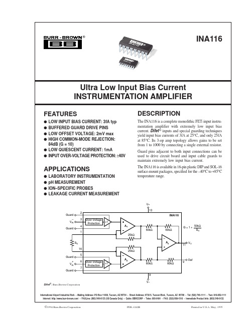
INA116
INA116
INA116
Ultra Low Input Bias Current INSTRUMENTATION AMPLIFIER
FEATURES
q LOW INPUT BIAS CURRENT: 3fA typ q BUFFERED GUARD DRIVE PINS q LOW OFFSET VOLTAGE: 2mV max q HIGH COMMON-MODE REJECTION:
84dB (G = 10) q LOW QUIESCENT CURRENT: 1mA q INPUT OVER-VOLTAGE PROTECTION: ±40V
APPLICATIONS
q LABORATORY INSTRUMENTATION q pH MEASUREMENT q ION–SPECIFIC PROBES q LEAKAGE CURRENT MEASUREMENT
DESCRIPTION
The INA116 is a complete monolithic FET-input instrumentation amplifier with extremely low input bias current. Difet ® inputs and special guarding techniques yield input bias currents of 3fA at 25°C, and only 25fA at 85°C. Its 3-op amp topology allows gains to be set from 1 to 1000 by connecting a single external resistor.
克伊利·7002开关系统数据手册说明书

1.888.KEITHLEY (U.S. only) SideTextSWITCHINGANDCONTROLA G R E A T E R M E A S U R E O F C O N F I D E N C ETen-slothighdensityswitchmainframe The Model 7002 Switch System is a 10-slot mainf rame that supports up to400 2-pole mul t i p lex e r channels or 400 matrix crosspoints. The front panelincludes a unique in t er a c t ive display of chan n el status for quick pro g ram-ming. Scanning speeds of up to 300 channels per second are possible withthe high density switch cards. The wide selection of more than 30 d ifferentswitch cards makes the 7002 one of the most flexible switch i ng main-frames avail a ble.Reduce the Size and Costof Your Switching Application.up to 400 channels of 2-pole switching. A single Model 7002 mainframecan accommodate up to ten 40-channel cards. That’s 400 channels in asingle full-rack package that is only 178mm high (7 in). This level of density provides some impor-tant advantages. First, it reduces the amount of switching hardware required for a given ap p li c a t ion. Second, it provides high flexibility. The high density cards can be used with the special signal cardsto cover all your signal needs for a large application with one m ainframe.The 7002 is fully compatible with all 7001 switch cards. From thisf ig u r a t ion flex i b il-a m p le, the outputs of a mul t ip lex e r card can be connectedt i p lex e r cards can be con n ect e d to formlex e r. Intercard wiring is eliminated by using the an a l og backplane to formThe interactive front panel display helps shorten the time requiredAn optional light pen provides point and click pro g ram m ing from thep lete switch patterns.Automatic card configuration. When the high density cards are installed,the 7002 au t o m at i c al l y configures each slot independently for the propercard. The channel status display on the front panel adjusts to show eachcard’s capacity and con f ig u r a t ion.Front panel info key. At the touch of a button, the operator receives con-text-sensitive, on-line information to help configure the system. This infor-mation is displayed on a 52-character alphanumeric display for clear andreadable messages. There is no need to refer constantly to the operator’smanual. All information messages, operating instructions, and prompts areavailable in English, German, and French. Just select the desired languagein the con f ig u r a t ion menu.Programmable channel closure restrictions. The 7002 allows specificchannels to be locked out from closure. This restriction can be conditionalbased on the open/close state of other channels or crosspoints. This capa-bility is useful to prevent certain signals from being accidentally connectedto high power circuits, for example.DC, RF, and optical switchcapabilityInteractive channel statusdisplaySERVICES AVAILABLE7002-3Y-EW 1-year factory warranty extended to 3 years from date of shipment19811.888.KEITHLEY (U.S. only)A G R E A T E R M E A S U R E O F C O N F I D EN CE7002 7002Switch/Control Mainframe400-channelSystem Throughput300 channel per second scanning. The 7002 can scan through up to 300 chan-nels per second. This scan process can be controlled by the internal time base of the 7002 or through external triggers. The scan sequence is con t rolled by what appears in the scan list. The scan list can include channels, ranges of channels, and memory locations. This ap p roach gives max i m um flexibility while obtaining maximum through p ut.Built-in Scan Control and trigger Link. The built-in scan control eliminates the need for the computer to control every step of the test pro-cedure. Simply program the 7002 to control the channel spacing, scan spacing, and number of scans. Trigger Link gives you access to six inde-pen d ent hardware trigger lines on a single cable.SYSTEMCAPACitY: 10 plug-in cards per mainframe.MeMoRY: Battery backed-up storage for 500 switch pat t erns. SWitCh SettLiNg tiMe: Automatically selected by the main-frame. For different switchcards, 7002 will be set to the slow-est relay settling time. Additional time from 0 to 99999.999s econds can be added in 1ms increments.tRiggeR SouRCeS:External Trigger (TTL-compatible, programmable edge, 600ns min i m um pulse, rear panel BNC).IEEE-488 bus (GET, *TRG)Trigger LinkTHROUGHPUTeXeCutioN SPeeD oF SCAN LiSt (channels or memory l ocationsper s econd):ChannelsMemoriesBreak-Before-MakeOFF 300243ON 270189tRiggeR eXeCutioN tiMe (maximum time from ac t i v a t ion of trig g er Source to start of switch open or close 2):Source Latency Jitter GET1 200 µs <15 µs *TRG2, 3 3.0 ms Trigger Link 200 µs <10 µs External200 µs<10 µs Timer <25 µsNOTES1. Excluding switch settling time.2. Assuming no IEEE-488 commands are pending execution.3. Display off.IEEE-488 COMMAND EXECUTION TIMECommand Execution Time 1CLOS (@1!1)<8 ms + Relay Settle Time NOTES1. Measured from the time at which the command terminator is taken from the bus to relay energize. With display OFF.IEEE-488 BUS IMPLEMENTATIONStANDARDS CoNFoRMANCe: Conforms to SCPI-1990, IEEE-488.2, and IEEE-488.1.MuLtiLiNe CoMMANDS: DCL, LLO, SDC, GET, GTL, UNT, UNL, SPE, SPD.uNiLiNe CoMMANDS: IFC, REN, EOI, SRQ, ATN.iNteRFACe FuNCtioNS: SH1, AH1, T5, TE0, L4, LE0, SR1, RL1, PP0, DC1, DT1, C0, E1.All aspects of 7002 op e r a t ion are available from the front panel or over the IEEE-bus interface. The 7002 conforms to IEEE-488.2 and the SCPI (Standard Com m ands for Programmable Instru m ents) command language protocol.• Scan List • Scan Spacing • Channel Spacing • Number of Scans • Number of Channels • Trigger Source• Single Channel Mode • Channel Restrictions • Save Mainframe Con f ig u r a t ion Setups • Digital I/O • Card Pair • Channel Delay • Number of Poles• Channel Pattern MemoryGENERALDiSPLAY: Dual-line vacuum fluorescent. 1st line: 20-char-ac t er alphanumeric. 2nd line: 32-character alphanu-meric. Chan n el status LED grid.Light PeN oPtioN: Provides interactive programming of channels, cross points, scan lists, and memory.ReAR PANeL CoNNeCtoRS: IEEE-488; 9-pin DB9 Female; 8-pin micro DIN for Trigger Link; 8-pin micro DIN for Trigger Link expansion; BNC for External Trigger; BNC for Channel ReadyPoWeR: 100V to 240Vrms, 50/60Hz, 110VA max i m um.eMC: Complies with European Union Directive 89/336/ EEC, EN61326-1.SAFetY: Conforms to European Union Directive 73/23/EEC, EN61010-1).eMi/RFi: Meets VDE 0871B and FCC Class B.eNViRoNMeNt: operating: 0°C to 50°C, <80% RH (0°C to 35°C). Storage: –25°C to +65°C.DiMeNSioNS, Weight: 178mm high × 438mm wide × 448mm deep (7 in × 171⁄4 in × 175⁄8 in). Net weight 9.1kg (20 lb).。
7002说明书

‡ SIGNET 7002 Vortex Flow SensorENGLISH3-7002.090DescriptionThe 3-7002 Vortex Flow Sensor uses vortex shedding technology as the primary method of determining the flow rate, and uses ultrasonic sensors to detect the vortices.The only material in contact with the fluid is PVDF plastic.It is available in 3 in. (DN80) and 4 in. (DN100) sizes, and in Wafer and Flanged versions. Both ANSI and ISO bolt patterns are offered.Location •Six common piping systems are shown as guidelines to help you select the best location for the vortex flow sensor. Always maximize distance between sensors and pump sources.Installation •All mounting angles are acceptable in either horizontal or vertical pipe runs, with upward flow preferred in the case of vertical runs. Install the sensor with the arrow pointing in the direction of the flow.•Pipe supports are recommended before and after the sensor to support the weight.*Install a "drip loop" or slope the conduit downward from the terminal block. Seal conduit entries with electrician's putty.•Reynold’s Number •value of 20000 is required in a 4 in. (DN 100) system.on flow sensor performance. As the viscosity of a fluid increases, the velocity (or flow rate) required to achieve accurate flow measurement also increases.application.Reynold’s Number:R e = 3162.76 x Q x Sg/(µ x ID)where:Q = Flow rate in GPMSg = Specific Gravityµ = Dynamic Viscosity in Centipoise (cP)ID = pipe inside diameter in inchesBackpressure Calculation •Minimum downstream pipe backpressure levels are required to prevent cavitation within the sensor. The minimum back pressure is calculated by the following formula: 2.7 x ∆P + 1.3x Po (∆P = Pressure drop across sensor. Po = Water saturation vapor pressure at operating temperature.)ing Pressure Drop Graph, find ∆P by locating yourmaximum flow rate on specific sensor size ing the Water Saturation Vapor Pressures Chart, find Po atoperating temperature.3.Calculate minimum back pressure needed using formula.Pressure Drop GraphC-7/02 EnglishInstallation•Proper alignment of the sensor with gaskets and flanges is necessary to assure a uniform flow profile through the sensor.•Space flanges in the piping system according to the length of the vortex flow sensor body.•Observe torque recommendations.•Mounting hardware, gaskets and piping system components (shown with broken lines in the diagrams below) are not furnished with the vortex flow sensors.•For flange versions: Bolt length approximations shown in the table above include two flange adapters, two flange rings and a gasket, all typical of +GF+ SYGEF-PVDF piping systemcomponents, plus nuts and washers.•For wafer versions: If the application requires operationoutside the range 15 to 35° C (59 to 95° F), then the accessory Spring Kit (3-7002.391) is necessary to relieve the forces due to thermal expansion of PVDF material and/or to prevent leakage during cooling. Bolt length approximations shown in the table above include sensor length, width dimensions for two each flange adapters, flange rings and gaskets, all typical of +GF+ SYGEF-PVDF piping system components, plus nuts and washers. If the accessory Spring Kit will be used, bolt length requirements increase by 60.0 mm (2.5 inches.)•Do not exceed 70 ºC media temperature •Do not exceed torque specifications.Sensor Config.# of Bolts Bolt Diameter Approximate Bolt Length Required Torque 3" Flange ISO 16M16 (5/8" - 11)70 mm (2.75")40 ± 5 N•m ( 30 ± 4 lbf•ft)3" Flange ANSI 8M16 (5/8" - 11)70 mm (2.75")40 ± 5 N•m ( 30 ± 4 lbf•ft)4" Flange ISO 16M16 (5/8" - 11)80 mm (3.00")45 ± 5 N•m (33 ± 4 lbf•ft)4" Flange ANSI 16M16 (5/8" - 11)80 mm (3.00")45 ± 5 N•m (33 ± 4 lbf•ft)3" Wafer ISO 8M16 (5/8" - 11)180 mm (7.50")25 N•m (18.5 lbf•ft)3" Wafer ANSI 4M16 (5/8" - 11)180 mm (7.50")25 N•m (18.5 lbf•ft)4" Wafer ISO 8M16 (5/8" - 11)220 mm (8.50")30 N•m (22 lbf•ft)4" WaferANSI8M16 (5/8" - 11)220 mm (8.50")30 N•m (22 lbf•ft)Tighten the flange bolts in the appropriate sequence.Tighted each bolt to 50% of the specification, repeat the pattern to 80%, then repeat again to the specified torque.Wiring for Frequency OutputThe open-collector frequency output requires a three-wire connection between the sensor and the monitoring device.To wire the vortex sensor frequency output to remote equipment:•Cable with single twisted-pair plus shield recommended.•Maximum cable length 200 ft.•Install cable through a conduit port andconnect as shown to the terminal block inside the vortex sensor cap.•Open collector voltage is supplied by +GF+ SIGNET instruments.•Use the 2535/2536 input card setting when wiring to the +GF+ SIGNET 9010Intelek-Pro Flow ControllerTo wire the vortex sensor frequency output to a Signet 8550Integral transmitter:cap. The cap will not be used.• Connect the Vortex sensor to the 8550 as shown.Out toremote equipmentCalibration Data: Frequency OutputUse the following K-factor data to program a flow meter which accepts the open collector frequency signal from the vortex flow sensor.The K-factor is the number of pulses generated byeach gallon (or liter) of fluid that passes through the sensor.Calibration - Current OutputThe current output from the 3-7002 is factory-calibrated for full scale operation ( 4-20 mA = 0-4 m/s).Since the sensor is limited to a minimum of 0.2 m/s, the current output is held at 4 mA when flow is less than 0.2 m/s, (or 0.66 ft/s), and increases to 20 mA at the maximum flow velocity (4.0 m/s, or 13.12 ft/s).The charts on page 5 show the relationship between the fluid velocity, the actual flow rate (in GPM and LPM) and the current output. You can also use the following formula to calculate the current output at any specific flow velocity.Example 1: In a pipe with a flow velocity of 2 m/s, what is the correct current output?:+4=12.0mAMax sensor velocityFluid velocity in pipe X 16+4=current output (mA)4 mA20 mAWiring for Current OutputThe 4-20 mA current output selection requires a two-wire loop connection between the sensor and monitoring device.+ 4 = 10.97 mAExample 2: In a 4 in.pipe what should the current output be when the flow rate is 200 gpm?:Velocity-Flow Rate-Current output ChartTechnical DataWetted materials•Sensor body:PVDFPipe size•d90/DN80 (3 in.) and d110/DN100 (4 in.) Linear Flow rangeTurn-down ratio:20:1•d90/DN80 (3 in.):Reynolds ≥ 16000: 0.2 to 4 m/s (0.66 to 13 ft/s)•d110/DN100 (4 in.):Reynolds ≥ 20000: 0.2 to 4 m/s (0.66 to 13 ft/s)NOTE: Below these velocity ranges, Vortex output is non-linear.Electronics module enclosure•Rating:NEMA 4X/IP65•Material:Valox®[Polybutylene TerephThalate (PBT) resin]Weight:Wafer 3 in./DN80: 4.5 lb/2.0 kg4 in./DN 100:7.0 lb./3.2 kgFlange: 3 in./DN80:11.0 lb./5.0 kg4 in./DN100:16.0 lb./7.3 kgElectrical•Accuracy:±1% of reading•Repeatability:±0.25% of reading•Response time: 1 s., first order5 s. settled to 1% of rate •Reverse polarity protection•Open Collector output:•NPN transistor, 10 mA max sink, 30 VDC max pull-up voltage, 0 to 100 Hz, 50% duty cycle, non-isolated.< 100 hz at maximum range.•Power requirement:4.5 to 7 VDC, regulated, 10 mA maximum•Current output:•factory-set; 4 to 20 mA = 0 to 4 m/s (0 to 13 ft/s) (Custom ranges available from factory)•Loop impedance:1Ω maximum at 12 VDC600Ω maximum at 24 VDC •Resolution:≈2.5 µA•Power requirement:12 to 24 VDC, regulated, 20 mA maximum268111417psibar32¡FWafer Vortex Sensor:10bar@30¼C,6.5bar@70¼C(145psi@86¼F,94psi@158¼F) Flange Vortex Sensor:10bar@30¼C,2bar@120¼C(145psi@86¼F,30psi@248¼F) EnvironmentalRating:NEMA 4X/IP65Maximum Media Pressure/Temperature•Ambient temp.:0 to 70 °C (32 to 158 °F)•Storage temp.:-15 to 80 °C (5 to 176 °F)•Relative humidity:0 to 95%, non-condensing •Vibration resistance:At least 1g in every axis up to 500 Hz.(The ultrasonic pickup is unaffected by normal piping system vibrations.)Standards and Approvals•Manufactured under ISO 9001 and ISO 14001•CE3-7000-5x3-7001-5xFlange Vortex Sensor dimensionsSize m m inch m m inch m m inch m m inch DN80133.1 5.2478.0 3.07108.0 4.25251.79.91DN100158.06.2296.03.78127.05.00277.110.91ABC DWafer Vortex Sensor dimensionsSizem m inch m m inch m m inch m m inch DN80196.97.7578.0 3.07199.97.87287.011.3DN100228.69.0096.03.78249.99.84322.612.7A BC D+GF+ SIGNET 7002 Vortex Flow SensorsPart NumberCodeDescription3-7002-2AF 159 000 6573-7002-2AFI 159 000 6583-7002-2AW159 000 6613-7002-2BF 159 000 662High-Purity 4” (d110/DN100) Flange, ANSI 3-7002-2BFI 159 000 663High-Purity 4” (d110/DN100) Flange, ISO 3-7002-2BW159 000 666High-Purity 4” (d110/DN100) Wafer3-7002-3AF 159 000 667PVDF 3” (d90/DN80) Flange, ANSI3-7002-3AFI 159 000 668PVDF 3” (d90/DN80) Flange, ISO 3-7002-3AW159 000 671PVDF 3” (d90/DN80) Wafer3-7002-3BF 159 000 672PVDF 4” (d110/DN100) Flange, ANSI 3-7002-3BFI 159 000 673PVDF 4” (d110/DN100) Flange, ISO 3-7002-3BW159 000 676PVDF 4” (d110/DN100) WaferAccessoriesPart NumberCodeDescription3-8550-1159 000 210Flow Transmitter for Field Mount3-8550-2159 000 212Flow Transmitter with 2 Relays for Field Mount 3-8550-3159 000 2142-Channel Flow Transmitter for Field Mount 3-8050159 000 184Universal Adapter Kit3-0000.393159 000 618Liquid Tight Connector Kit with PG 13.5 to NPT Adapter 3-7002.391159 000 692Spring Kit (includes four (4) springs)Ordering Information‡ SIGNETSignet Scientific Company, 3401 Aerojet Avenue, El Monte, CA 91731-2882 U.S.A. • Tel. (626) 571-2770 • Fax (626) 573-2057For Worldwide Sales and Service, visit our website: • Or call (in the U.S.): (800) 854-4090GEORGE FISCHER ‡ Piping Systems3-7002.090/(C-7/02) English© Signet Scientific Company 2002Printed in U.S.A. on recycled paper。
T1620-600W;T1620-700W;T1630-600W;中文规格书,Datasheet资料

October 2011Doc ID 3759 Rev 11/8T1620W, T1630WSnubberless™ 16A TriacsFeatures■I T(RMS) = 16 A■V DRM / V RRM = 600, 700 and 800 V ■I GT = 20 to 30 mADescriptionBased on ST’s Snubberless technology providing high commutation performances, theT1620-600W/700W/800W and T1630-600W are especially recommended for use with inductive loads such as rice cookers. They comply with UL standards (ref. E81734).TM : Snubberless is a trademark of STMicroelectronicsCharacteristics T1620W, T1630W2/8Doc ID 3759 Rev 11 CharacteristicsTable 1.Absolute maximum ratingsSymbol ParameterValue Unit I T(RMS)On-state rms current (full sine wave)T c = 80 °C 16A I TSM Non repetitive surge peak on-state current (full cycle, T j initial = 25 °C) F = 50 Hz t = 20 ms 200A F = 60 Hz t = 16.7 ms218I ²t I ²t Value for fusingt p = 10 ms220A ²s dI/dtCritical rate of rise of on-state current I G = 2 x I GT , t r≤ 100 nsF = 120 HzT j = 125 °C 50A/µs V DSM /V RSM Non repetitive surge peak off-statevoltage t p = 10 ms T j = 25 °C V DRM /V RRM+ 100V I GM Peak gate currentt p = 20 µsT j = 125 °C 4A P G(AV)Average gate power dissipation T j = 125 °C 1W T stgT jStorage junction temperature range Operating junction temperature range- 40 to + 150- 40 to + 125°CTable 2.Electrical characteristics (T j = 25 °C, unless otherwise specified)Symbol Test conditionsQuadrantValueUnitT1620T1630I GT (1)V D = 12 V R L = 30 ΩI - II - III MAX.2030mA V GT I - II - III MAX. 1.3V V GD V D = V DRM , R L = 3.3 k Ω, T j = 125 °C I - II - IIIMIN.0.2V I H (2)I T = 250 mA MAX.3550mA I LI G = 1.2 I GTI - III MAX.7080mA II 80100dV/dt (2)V D = 67% V DRM, gate open, T j = 125 °C MIN.300500V/µs (dI/dt)c(2)Without snubber, T j = 125 °CMIN.8.511A/ms 1.minimum I GT is guaranted at 5% of I GT max.2.for both polarities of A2 referenced to A1.T1620W, T1630W CharacteristicsDoc ID 3759 Rev 13/8Table 3.Static characteristicsSymbol Test conditionsValue Unit V T (1)I TM = 22.5 A, t p = 380 µs T j = 25 °C MAX. 1.4V V TO (1)Threshold voltage T j = 125 °C MAX.0.85V R D (1)Dynamic resistance T j = 125 °C MAX.250m ΩI DRM I RRMV DRM = V RRMT j = 25 °C MAX.5µA T j = 125 °C1mA1.for both polarities of A2 referenced to A1.Table 4.Thermal resistanceSymbol ParameterValue Unit R th(j-c)Junction to case (AC) (360° conduction angle) 3.1 °C/W R th(j-a)Junction to ambient60°C/WFigure 1.Maximum power dissipation versusFigure 2.On-state rms current versus caseFigure 3.Relative variation of thermalFigure 4.On-state characteristicsCharacteristicsT1620W, T1630W4/8Doc ID 3759 Rev 1Figure 9.Relative variation of critical rate of decrease of main current versus junctionFigure 5.Surge peak on-state current versus Figure 6.Non-repetitive surge peak on-state Figure 7.Relative variation of I GT ,I H , I L vs junction temperature Figure 8.Relative variation of critical rate of decrease of main current versusT1620W, T1630W Ordering information schemeDoc ID 3759 Rev 15/82 Ordering information schemeTable 5.Product SelectorPart Numbers Voltage (xxx)SensitivityTypePackage600 V700 V800 VT1620-600W X20 mASnubberless ISOWA TT220ABT1620-700W XT1620-800W XT1630-600WX30 mAPackage mechanical data T1620W, T1630W3 Package mechanical data●Epoxy meets UL94, V0●Recommended torque 0.4 to 0.6 N·mIn order to meet environmental requirements, ST offers these devices in different grades ofECOPACK® packages, depending on their level of environmental compliance. ECOPACK®specifications, grade definitions and product status are available at: .ECOPACK® is an ST trademark.6/8Doc ID 3759 Rev 1T1620W, T1630W Ordering InformationDoc ID 3759 Rev 17/84 Ordering Information5 Revision historyTable 7.Ordering informationOrder code Marking PackageWeightBase qtyDelivery modeT1620-600W T1620600W ISOWA TT220AB2.3 g50TubeT1620-700W T1620700W T1620-800W T1620800W T1630-600WT1630600WTable 8.Document revision historyDate RevisionChangesMar-20042Last update.18-Oct-20113Insert T1620-700W, Insert 700 V in fig.10,deleted T1630-800W.T1620W, T1630WPlease Read Carefully:Information in this document is provided solely in connection with ST products. STMicroelectronics NV and its subsidiaries (“ST”) reserve the right to make changes, corrections, modifications or improvements, to this document, and the products and services described herein at any time, without notice.All ST products are sold pursuant to ST’s terms and conditions of sale.Purchasers are solely responsible for the choice, selection and use of the ST products and services described herein, and ST assumes no liability whatsoever relating to the choice, selection or use of the ST products and services described herein.No license, express or implied, by estoppel or otherwise, to any intellectual property rights is granted under this document. If any part of this document refers to any third party products or services it shall not be deemed a license grant by ST for the use of such third party products or services, or any intellectual property contained therein or considered as a warranty covering the use in any manner whatsoever of such third party products or services or any intellectual property contained therein.UNLESS OTHERWISE SET FORTH IN ST’S TERMS AND CONDITIONS OF SALE ST DISCLAIMS ANY EXPRESS OR IMPLIED WARRANTY WITH RESPECT TO THE USE AND/OR SALE OF ST PRODUCTS INCLUDING WITHOUT LIMITATION IMPLIED WARRANTIES OF MERCHANTABILITY, FITNESS FOR A PARTICULAR PURPOSE (AND THEIR EQUIVALENTS UNDER THE LAWS OF ANY JURISDICTION), OR INFRINGEMENT OF ANY PATENT, COPYRIGHT OR OTHER INTELLECTUAL PROPERTY RIGHT. UNLESS EXPRESSLY APPROVED IN WRITING BY TWO AUTHORIZED ST REPRESENTATIVES, ST PRODUCTS ARE NOT RECOMMENDED, AUTHORIZED OR WARRANTED FOR USE IN MILITARY, AIR CRAFT, SPACE, LIFE SAVING, OR LIFE SUSTAINING APPLICATIONS, NOR IN PRODUCTS OR SYSTEMS WHERE FAILURE OR MALFUNCTION MAY RESULT IN PERSONAL INJURY, DEATH, OR SEVERE PROPERTY OR ENVIRONMENTAL DAMAGE. ST PRODUCTS WHICH ARE NOT SPECIFIED AS "AUTOMOTIVE GRADE" MAY ONLY BE USED IN AUTOMOTIVE APPLICATIONS AT USER’S OWN RISK.Resale of ST products with provisions different from the statements and/or technical features set forth in this document shall immediately void any warranty granted by ST for the ST product or service described herein and shall not create or extend in any manner whatsoever, any liability of ST.ST and the ST logo are trademarks or registered trademarks of ST in various countries.Information in this document supersedes and replaces all information previously supplied.The ST logo is a registered trademark of STMicroelectronics. All other names are the property of their respective owners.© 2011 STMicroelectronics - All rights reservedSTMicroelectronics group of companiesAustralia - Belgium - Brazil - Canada - China - Czech Republic - Finland - France - Germany - Hong Kong - India - Israel - Italy - Japan - Malaysia - Malta - Morocco - Philippines - Singapore - Spain - Sweden - Switzerland - United Kingdom - United States of America8/8Doc ID 3759 Rev 1分销商库存信息:STMT1620-600W T1620-700W T1630-600W。
RK7002AT116中文资料

Transistors Rev.A 1/44V Drive Nch MOS FETRK7002Az StructureSilicon N-channel MOS FET transistorz Features1) Low on-resistance. 2) High ESD3) High-speed switching. 4) Low-voltage drive (4V).5) Drive circuits can be simple.6) Parallel use is easy .z ApplicationsSwitching z External dimensions (Unit : mm)z Packaging specifications z Equivalent circuitRK7002AType T1163000Package CodeBasic ordering unit (pieces)TapingA protection diode has been built in between thegate and the source to protect against static electricity when the product is in use.Use the protection circuit when fixed voltages are exceeded.z Absolute maximum ratings (T a=25°C)Drain-source voltage Gate-source voltage Drain current Source current (Body diode)Total power dissipation Channel temperature Storage temperatureContinuous Pulsed Continuous PulsedV DSS V GSS I S P D ∗2Tch 60V V mA mA mW °C ±20 ±300I D I SP ∗1A I DP ∗1A ±1.22000.8200150Tstg°C−55 to +150Symbol Limits Unit Parameter∗1 Pw ≤10µs, Duty cycle ≤1%∗2 With each pin mounted on the recommended land.z Thermal resistance°C / WRth (ch-a)625ParameterSymbol Limits Unit Channel to ambientWith each pin mounted on the recommended land.∗Transistors Rev.A 2/4z Electrical characteristics (T a=25°C)z Body diode characteristics (Source-Drain) (T a=25°C)Forward voltageV SD −− 1.2V I S =300mA, V GS =0VParameterSymbol Min.Typ.Max.Unit Conditions∗Pulsed∗Transistors Rev.A 3/4z Electrical characteristic curvesFig.1 Typical output characteristics D R A I N C U R R E N T : I D (A )DRAIN-SOURCE VOLTAGE : V DS (V)GATE-SOURCE VOLTAGE : V GS (V)Fig.2 Typical transfer characteristicsD R A I N C U R RE N T : I D (A )CHANNEL TEMPERATURE : Tch (°C)G A T E T H R E S HO L D V O L T A G E : V G S (t h ) (V )Fig.3 Gate threshold voltagevs. channel temperatureDRAIN CURRENT : I D (A)Fig.4 Static drain-source on-stateresistance vs. drain current ( Ι )S T A T I C D R A I N -S O U R C E O N -S T A T E R E S I S T A N C E : R D S (o n ) (Ω)DRAIN CURRENT : I D (A)Fig.5 Static drain-source on-stateresistance vs. drain current ( ΙΙ )S T A T I C D R A I N -S O U R C E O N -S T A T E R E S I S T A N C E : R D S (o n ) (Ω)Fig.6 Static drain-source on-stateresistance vs. gate-source voltage7563214GATE-SOURCE VOLTAGE : V GS (V)O N -S T A T E R E S I S T A N C E : R D S (o n ) (Ω)S T A T I C D R A I N -S O U R C ES T A T I C D R A I N -S O U R C E O N -S T A T ER E S I S T A N C E : R D S (o n ) (Ω)CHANNEL TEMPERATURE : Tch (°C)Fig.7 Static drain-source on-stateresistance vs. channel temperatureSOURCE-DRAIN VOLTAGE : V SD (V)Fig.8 Reverse drain current vs.source-drain voltage ( Ι )R E V E R S E D R A I N C U R R E N T : I D R (A )SOURCE-DRAIN VOLTAGE : V SD (V)Fig.9 Reverse drain current vs.source-drain voltage ( ΙΙ )R E V E R S E D R A I N C U R R E N T : I D R (A )Transistors Rev.A 4/4Fig.10 Forward transfer admittancevs. drain currentF O R W A R D T R A N S F E R A D M I T T A N C E : |Y f s | (S )DRAIN CURRENT : I D (A)Fig.11 Typical capacitancevs. drain-source voltageC A P A C I T A N C E : C (p F )DRAIN-SOURCE VOLTAGE : V DS (V)S W I T C H I N G T I M E : t (n s )DRAIN CURRENT : I D (A)Fig.12 Switching characteristics(See Figures 13 and 14 for the measurement circuit and resultant waveforms)z Switching characteristics measurement circuitFig.13 Switching time measurement circuit DSFig.14 Switching time waveformsAppendixAbout Export Control Order in JapanProducts described herein are the objects of controlled goods in Annex 1 (Item 16) of Export T rade ControlOrder in Japan.In case of export from Japan, please confirm if it applies to "objective" criteria or an "informed" (by MITI clause)on the basis of "catch all controls for Non-Proliferation of Weapons of Mass Destruction.Appendix1-Rev1.1。
SN7002中文资料
lki
gj
f h
j kl
5.0 6.0 7.0 8.0 9.0 10.0 b
0.00 0.04 0.08 0.12 0.16
A
0.24
ID
Typ. transfer characteristics ID = f(VGS) parameter: tp = 80 µs
Typ. forward transconductance gfs = f (ID) parameter: tp = 80 µs,
-
0.1
1
VDS = 60 V, VGS = 0 V, Tj = 125 °C
-
-
5
Gate-source leakage current
IGSS
VGS = 20 V, VDS = 0 V
-
1
10
Drain-Source on-state resistance
RDS(on)
VGS = 10 V, ID = 0.5 A
V(BR)DSS
VGS = 0 V, ID = 0.25 mA, Tj = 25 °C
60
-
-
Gate threshold voltage
VGS(th)
VGS=VDS, ID = 1 mA
0.8
1.4
2
Zero gate voltage drain current
IDSS
VDS = 60 V, VGS = 0 V, Tj = 25 °C
0.40
W
Ptot 0.32 0.28
0.24
0.20
0.16
0.12
0.08
0.04
0.00 0
20 40 60 80 100 120 °C 160
2N7002KT1G中文资料

2N7002KSmall Signal MOSFET60 V, 380 mA, Single, N−Channel, SOT−23 Features•ESD Protected•Low R DS(on)•Surface Mount Package•This is a Pb−Free DeviceApplications•Low Side Load Switch•Level Shift Circuits•DC−DC Converter•Portable Applications i.e. DSC, PDA, Cell Phone, etc. MAXIMUM RATINGS (T J = 25°C unless otherwise stated)Rating Symbol Value Unit Drain−to−Source Voltage V DSS60V Gate−to−Source Voltage V GS±20VDrain Current (Note 1)Steady State T A = 25°CT A = 85°Ct < 5 s T A = 25°CT A = 85°C I D320230380270mAPower Dissipation (Note 1) Steady Statet < 5 s P D300420mWPulsed Drain Current (t p = 10 m s)I DM 1.5AOperating Junction and Storage Temperature Range T J, T STG−55 to+150°CSource Current (Body Diode)I S300mALead Temperature for Soldering Purposes (1/8″ from case for 10 s)TL260°CGate−Source ESD Rating(HBM, Method 3015)ESD2000VStresses exceeding Maximum Ratings may damage the device. Maximum Ratings are stress ratings only. Functional operation above the Recommended Operating Conditions is not implied. Extended exposure to stresses above the Recommended Operating Conditions may affect device reliability. THERMAL CHARACTERISTICSCharacteristic Symbol Max Unit Junction−to−Ambient − Steady State(Note1)R q JA417°C/W Junction−to−Ambient − t ≤ 5 s (Note 1)R q JA3001.Surface−mounted on FR4 board using 1 in sq pad size (Cu area = 1.127 insq [1 oz] including traces)Device Package Shipping†ORDERING INFORMATION2N7002KT1G3000/T ape & ReelSimplified SchematicSOT−23CASE 318STYLE 21704 M GGMARKING DIAGRAM& PIN ASSIGNMENT321DrainGate SourceSOT−23(Pb−Free)60 V 1.6 W @ 10 VR DS(on) MAX380 mAI D MAX(Note 1)V(BR)DSS†For information on tape and reel specifications, including part orientation and tape sizes, please refer to our T ape and Reel Packaging Specifications Brochure, BRD8011/D.2.5 W @ 4.5 VGateSourceDrain(Top View)704= Specific Device CodeM= Date CodeG= Pb−Free Package(Note: Microdot may be in either location) *Date Code orientation and/or position mayvary depending upon manufacturing location.ELECTRICAL CHARACTERISTICS (T J = 25°C unless otherwise specified)Parameter Symbol Test Condition Min Typ Max Units OFF CHARACTERISTICSDrain−to−Source Breakdown Voltage V(BR)DSS V GS = 0 V, I D = 250 m A60V Drain−to−Source Breakdown VoltageTemperature CoefficientV(BR)DSS/T J71mV/°CZero Gate Voltage Drain Current I DSS VGS = 0 V,V DS = 60 V T J = 25°C1m A T J = 125°C500V GS = 0 V,V DS = 50 VT J = 25°C100nA Gate−to−Source Leakage Current I GSS V DS = 0 V, V GS = ±20 V±10m AV DS = 0 V, V GS = ±10 V450nAV DS = 0 V, V GS = ±5.0 V150nA ON CHARACTERISTICS (Note 2)Gate Threshold Voltage V GS(TH)V GS = V DS, I D = 250 m A 1.0 2.5V Negative Threshold TemperatureCoefficientV GS(TH)/T J 4.0mV/°C Drain−to−Source On Resistance R DS(on)V GS = 10 V, I D = 500 mA 1.19 1.6WV GS = 4.5 V, I D = 200 mA 1.33 2.5Forward Transconductance g FS V DS = 5 V, I D = 200 mA80S CHARGES AND CAPACITANCESInput Capacitance C ISSV GS = 0 V, f = 1 MHz,V DS = 20 V 24.5pFOutput Capacitance C OSS 4.2 Reverse Transfer Capacitance C RSS 2.2Total Gate Charge Q G(TOT)V GS = 4.5 V, V DS = 10 V;I D = 200 mA 0.7nCThreshold Gate Charge Q G(TH)0.1 Gate−to−Source Charge Q GS0.3 Gate−to−Drain Charge Q GD0.1 SWITCHING CHARACTERISTICS, V GS = V (Note 3)Turn−On Delay Time t d(ON)V GS = 10 V, V DD = 25 V,I D = 500 mA, R G = 25 W 12.2nsRise Time t r9.0 Turn−Off Delay Time t d(OFF)55.8 Fall Time t f29 DRAIN−SOURCE DIODE CHARACTERISTICSForward Diode Voltage V SD VGS = 0 V,I S = 200 mA T J = 25°C0.8 1.2V T J = 85°C0.72.Pulse Test: pulse width ≤ 300 m s, duty cycle ≤ 2%3.Switching characteristics are independent of operating junction temperaturesFigure 1. On −Region CharacteristicsFigure 2. Transfer CharacteristicsV DS , DRAIN −TO −SOURCE VOLTAGE (V)V GS , GATE −TO −SOURCE VOLTAGE (V)Figure 3. On −Resistance vs. Drain Current andTemperatureFigure 4. On −Resistance vs. Drain Current andTemperatureI D , DRAIN CURRENT (A)Figure 5. On −Resistance vs. Gate −to −SourceVoltage Figure 6. On −Resistance Variation withTemperatureV GS , GATE −TO −SOURCE VOLTAGE (V)T J , JUNCTION TEMPERATURE (°C)I D , D R A I N C U R R E N T (A )I D , D R A I N C U R R E N T (A )R D S (o n ), D R A I N −T O −S O U R C E R E S I S T A N C E (W )R D S (o n ), D R A I N −T O −S O U R C E R E S I S T A N C E (W )R D S (o n ), D R A I N −T O −S O U R C E R E S I S T A N C E (N O R M A L I Z E D )I D , DRAIN CURRENT (A)R D S (o n ), D R A I N −T O −S O U R C E R E S I S T A N C E (W )Figure 7. Capacitance VariationFigure 8. Gate −to −Source andDrain −to −Source Voltage vs. Total ChargeQg, TOTAL GATE CHARGE (nC)Figure 9. Diode Forward Voltage vs. CurrentV SD , SOURCE −TO −DRAIN VOLTAGE (V)110V G S , G A T E −T O −S O U R C E V O L T A G E (V )I S , S O U R C E C U R R E N T (A )C , C A P A C I T A N C E (p F )GATE −TO −SOURCE OR DRAIN −TO −SOURCE VOLTAGE (V)0.1PACKAGE DIMENSIONSSOT −23 (TO −236)CASE 318−08ISSUE ANSTYLE 21:PIN 1.GATE2.SOURCE3.DRAINNOTES:1.DIMENSIONING AND TOLERANCING PER ANSI Y14.5M, 1982.2.CONTROLLING DIMENSION: INCH.3.MAXIMUM LEAD THICKNESS INCLUDES LEAD FINISHTHICKNESS. MINIMUM LEAD THICKNESS IS THE MINIMUM THICKNESS OF BASE MATERIAL.4.318−01 THRU −07 AND −09 OBSOLETE, NEW STANDARD 318−08.SOLDERING FOOTPRINTVIEW CDIM A MIN NOM MAX MINMILLIMETERS0.89 1.00 1.110.035INCHES A10.010.060.100.001b 0.370.440.500.015c 0.090.130.180.003D 2.80 2.90 3.040.110E 1.20 1.30 1.400.047e 1.78 1.90 2.040.070L 0.100.200.300.0040.0400.0440.0020.0040.0180.0200.0050.0070.1140.1200.0510.0550.0750.0810.0080.012NOM MAX L1 2.102.40 2.640.0830.0940.104H E0.350.540.690.0140.0210.029ON Semiconductor and are registered trademarks of Semiconductor Components Industries, LLC (SCILLC). SCILLC reserves the right to make changes without further noticeto any products herein. SCILLC makes no warranty, representation or guarantee regarding the suitability of its products for any particular purpose, nor does SCILLC assume any liability arising out of the application or use of any product or circuit, and specifically disclaims any and all liability, including without limitation special, consequential or incidental damages.“Typical” parameters which may be provided in SCILLC data sheets and/or specifications can and do vary in different applications and actual performance may vary over time. All operating parameters, including “Typicals” must be validated for each customer application by customer’s technical experts. SCILLC does not convey any license under its patent rights nor the rights of others. SCILLC products are not designed, intended, or authorized for use as components in systems intended for surgical implant into the body, or other applications intended to support or sustain life, or for any other application in which the failure of the SCILLC product could create a situation where personal injury or death may occur. Should Buyer purchase or use SCILLC products for any such unintended or unauthorized application, Buyer shall indemnify and hold SCILLC and its officers, employees, subsidiaries, affiliates,and distributors harmless against all claims, costs, damages, and expenses, and reasonable attorney fees arising out of, directly or indirectly, any claim of personal injury or death associated with such unintended or unauthorized use, even if such claim alleges that SCILLC was negligent regarding the design or manufacture of the part. SCILLC is an Equal Opportunity/Affirmative Action Employer. This literature is subject to all applicable copyright laws and is not for resale in any manner.PUBLICATION ORDERING INFORMATION。
欧博特纽维尔 IP7000系列产品数据手册说明书

From Product Management Telephone NurembergST-VS ST-VS/MKP1 +49 911 93456 0 12-Jan-2015 Release LetterProduct: DIVAR IP 7000 FamilyVersion: Maintenance Release DOM image v1.0.5This letter contains latest information about the above mentioned Bosch DIVAR IP 7000 Family.1. GeneralDIVAR IP 7000 is an affordable, simple and reliable all-in-one recording, viewing and management solution for network surveillance systems of up to 128 channels (with 32 channels pre-licensed).Running the full Bosch VMS (Video Management System) solution and powered by Bosch Video Recording Manager software, DIVAR IP 7000 is an intelligent IP storage device that eliminates the need for separate NVR (Network Video Recorder) server and storage hardware.It combines advanced recording management and state-of-the-art iSCSI storage into a single cost-effective, plug and play IP recording appliance for IT-minded customers which are seeking for a state-of-the-art “second generation” NVR recording solution.2. Restrictions; Known Issues•Graphics Port: The DVI port must be used for configuration. Do not use the VGA port for configuration.•Initial installation: During initial boot and installation the system must be connected to the network.Please note: All systems come with the same default IP address.•Transcoder: Maximum transcoder source stream resolution is 1920x1080p30•Mobile Video Service: the local MVS needs to be added to the system with the private IP address (not 127.0.0.1), if it shall serve as a fall-back transcoder for Operator Client access.•BVC needs to be upgraded to version 1.6.2 or higher, if it shall serve as replay client for DIVAR IP 7000 appliances with BVMS 5.0.5•VideoSDK needs to be upgraded to 5.81 MR1 or higher, if it shall serve as integration tool for DIVAR IP 3000 appliances with BVMS 5.0.5•3rd party device support restrictions are listed in the Bosch VMS release notes:o /documents/Release_Notes_5.0.5__Release_Note_enUS _16781064459.pdf3. New subcomponent software versions•Bosch VMS 5.0.5.1010 (alternative installation option: BVMS 4.5.9.359)From Product Management Telephone NurembergST-VS ST-VS/MKP1 +49 911 93456 0 12-Jan-2015•Video Recording Manager 3.00.0074•Video Streaming Gateway 5.91.0020•USB-Transcoder Service 5.60.00784. New FeaturesSystem Setup•Initial Setup procedure prompts a selection of two software installation options:o BVMS 5.0.5: recommended for most userso BVMS 4.5.9: recommended if system shall be integrated into existing BVMS 4.5.9 based infrastructureConfiguration Wizard (BVMS 5.0.5)•Remote access: DNS information can be entered in the Basic step. The port rules for router configuration can be retrieved from the detailed report in the last wizard step.•Network address of video devices to be added can be changed, if they are located in a different IP range.•Recording profiles and retention time settings can be changed individually per device or for a selection of devices.Management Server (BVMS 5.0.5)•Additional data: option to record text data together with video streamVideo Streaming Gateway (BVMS 5.0.5)•VSG supports alarm recording triggered by BVMS events5. Applied Changes / Bug FixesBVMS 5.0.5•Tested software/firmware versions, supported devices, bug fixes and change are listed in the Bosch VMS release notes:/documents/Release_Notes_5.0.5__Release_Note_enUS_16781 064459.pdfVideo Recording Manager•Bug fixes and change are listed in the VRM release notes:/downloads/nue-mkp/VRM/3_00/Bosch_Releaseletter_VRM3_00_0073.pdfMobile Video Service•Fixed: correct MVS entry shown in port mapping table for remote access•Fixed: local MVS priority settings prevent system overload•Changed: MVS web page can now be used: https://<system-IP>/mvsFrom Product Management Telephone NurembergST-VS ST-VS/MKP1 +49 911 93456 0 12-Jan-20156. Installation Notes•An upgrade from DOM Image v1.0.1 cannot be performed manually. DOM image v1.0.2 and later require a newer version of the system BIOS•All models are based on Windows Server 2008 R2, 64-bit, Standard Edition7. History7.1 DIVAR IP 7000 DOM image version 1.0.4Restrictions; Known Issues•Graphics Port: The DVI port must be used for configuration. Do not use the VGA port for configuration.•Initial installation: During initial boot and installation the system must be connected to the network.Please note: All systems come with the same default IP address.•Transcoder: Maximum transcoder source stream resolution is 1920x1080p30•ONVIF Support Restrictionso no support for event-based recordingo Audio on some 3rd Party cameras not fully supported which may result in non-availability of audio streamso TCP not supported for ONVIF cameras but with UDP protocol onlyo Motion JPEG is not supportedo VCA is always recorded for Bosch deviceso VCA is not available for ONVIF camerasFrom Product Management Telephone NurembergST-VS ST-VS/MKP1 +49 911 93456 0 12-Jan-2015New subcomponent software versions•BVMS 4.5.9.359•VRM 3.00.0057New FeaturesImage•Added support for 3TB hard drives (DIVAR IP 7000 2U)•Added support for party populated hard drive layouts; 3 to 8 hard drives as part of a RAID 5 configuration (DIVAR IP 7000 2U)Configuration Client and Configuration Wizard•To avoid security issues, a global default password must be set for all devices and all authorization levels (service, live, user) that are not password protected. You can disable this enforced password protection for BVIP devices.•VIP X16 XF E has been moved to Device Family 2 for support of 2nd stream for recording.Deviating from the behaviour of the other devices belonging to Device Family 2, VIP X16 XF Emust use the same stream for all recordings. Although the user can configure stream 1 forcontinuous recording and stream 2 for alarm recording, the second setting will not take effect. After an Bosch VMS upgrade, perform the update of the device family manually.To update the device family:Right-click the device and click Edit Encoder.Click OK.Applied Changes / Bug FixesImage•Fixed: DVD burner permission problem•Fixed: 30days password expiration problem (last fix didn’t apply in every case)•Changed: Client software and documentation updated on the local network share Operator Client•Fixed: Click on find video by event results jumped to wrong playback time.•Fixed: Live video images from NTSC cameras on DVR 670 were squeezed.•Fixed: Sometimes OpClient could crash on loading favorites.•Fixed: ONVIF domes could not be controlled.•Fixed: Under rare circumstances OpClient could crash on logon of dual authorization group.•Fixed: Video viewing via NAT/port mapping routes did not work on Windows XP.•Fixed: Manual focus/iris in automatic mode.•Tested software/firmware versions and supported devices (see BVMS 4.5.9 release notes for details http://144.76.6.227/downloads/support-cctv/DIVAR_IP_3000/BVMS_VERSION_4_5_9_ReleaseNotes.pdf)From Product Management Telephone NurembergST-VS ST-VS/MKP1 +49 911 93456 0 12-Jan-2015 Configuration Client•Fixed: OPC Server Connection for BIS license option was not available.Configuration Collector•Fixed: Config Collector freezed while zipping collected files.VRM•Fixed: Discovery is more stable•Fixed: Reliability of disconnecting transcoders improved•Fixed: Exporting Log-Files large than 100MB•Changed: iSCSI-password is also set on USB-Transcoder7.1 DIVAR IP 7000 DOM image version 1.0.2Restrictions; Known Issues•Graphics Port: The DVI port must be used for configuration. Do not use the VGA port for configuration.•Initial installation: During initial boot and installation the system must be connected to the network.Please note: All systems come with the same default IP address.•ONVIF Support Restrictionso no support for event-based recordingo Audio on some 3rd Party cameras not fully supported which may result in non-availability of audio streamso TCP not supported for ONVIF cameras but with UDP protocol onlyo Motion JPEG is not supportedo VCA is always recorded for Bosch deviceso VCA is not available for ONVIF camerasNew subcomponent software versions•BVMS 4.5.8.151•VSG 5.60.0073• Transcoder 5.60.0073•.NET Framework 4.5New Features•Unlisted Bosch BVIP video devices can be added as generic devices (see BVMS 4.5.5 release notes for details).•Server Lookup improvements (see BVMS 4.5.8 release notes for details).From Product Management Telephone NurembergST-VS ST-VS/MKP1 +49 911 93456 0 12-Jan-2015 •Minor changes in the user and workstation settings (see BVMS 4.5.8 release notes for details).•Client software and documentation can be downloaded from local network share.Applied Changes / Bug Fixes•Fixed: 30days password expiration problem•Fixed: Windows activation problem•Fixed: iSCSI LUN preparation problem•Fixed: firewall rule exceptions•Wizard prompts system reboot option when Network settings are changed•Minor fixes in new subcomponent software versions (BVMS, VRM, VSG, Transcoder)•Minor improvements in the initial installation procedure•Tested software/firmware versions and supported devices (see BVMS 4.5.8 release notes for details → http://144.76.6.227/downloads/support-cctv/DIVAR_IP_3000/BVMS_VERSION_4_5_8_ReleaseNotes_v1.pdf).•Bosch VMS default screen now shows text labels below the icons.•The default network settings now match the default network settings of other Bosch video devices o IP Address: 192.168.0.200o Subnet mask: 255.255.255.0Installation Notes•An upgrade from DOM Image v1.0.1 cannot be performed manually. DOM image v1.0.2 requires a newer version of the system BIOS•All models are based on Windows Server 2008 R2, 64-bit, Standard Edition7.2 DIVAR IP 7000 DOM image version 1.0.1Restrictions; Known Issues•Graphics Port: The DVI port must be used for configuration. Do not use the VGA port for configuration.•Password of limited operational Windows user expires after 30 days:o The password of limited user must be set manually to “never expires” on DIVAR IP 7000 by logging on to the DIVAR IP via remote desktop with user administrator user “BVRAdmin”.In the “Server Manager” the password can be changed to “Password never expires”(Configuration → Local Users and Groups → User (→ user limited)).o For details s. Bosch Security Knowledge Basehttps:///al/12/2/article.aspx?aid=7400&tab=search&bt=4&r= •Default IP Address: The system comes with the following network settingso IP Address: 192.168.178.200o Subnet mask: 255.255.0.0From Product Management Telephone NurembergST-VS ST-VS/MKP1 +49 911 93456 0 12-Jan-2015 •Initial installation: During initial boot and installation the system must be connected to the network.Please note: All systems come with the same default IP address.•Network Settings Change: The DIVAR IP needs to be restarted, if network settings are changed in the Wizard. This applies for the initial setup as well as for changes during standard operation.•Adding Storage: If the wizard stops at Step 8 “Add storage”, because the LUNs aren’t formatted, the LUNs have to be formatted using the Bosch VMS Config Client.•ONVIF Support Restrictionso no support for event-based recordingo Audio on some 3rd Party cameras not fully supported which may result in non-availability of audio streamso TCP not supported for ONVIF cameras but with UDP protocol onlyo Motion JPEG is not supportedo VCA is always recorded for Bosch deviceso VCA is not available for ONVIF camerasNew FeaturesThe DIVAR IP 7000 Family is an all-in-one management solution that comes with BVMS/VRM including Video Streaming Gateway pre-installed and with 32 channels pre-licensed. The system will come with one built-in Transcoder channel.Applied Changes / Bug Fixesn/a。
积层贴片陶瓷片式电容器商品说明书
此外,对使用本产品目录中所记载产品的设备进行设计时,请确保符合该设备的使用用途及状态的保护回路和装置,并设置备用回路等。 2. 本产品目录中记载的产品因改良及其他原因可能在不经预告的情况下进行变更或停止供应。 3. 关于本产品目录中记载的产品,本公司备有记载了各产品的规格及安全注意事项的 “ 交货规格书 ”。在选用产品时,建议签定交货规格
(例)
产品目录发行日期 2012 年12 月以前 2013 年1 月及以后
目录型号 C1608C0G1E103J(080AA) C1608C0G1E103J080AA
交货型号(交货标签上的标识) C1608C0G1E103JT000N C1608C0G1E103JT000N
20201025 / mlcc_commercial_general_zh.fm
长度 0.40 0.60 1.00 1.60 2.00 3.20 3.20 4.50 5.70
宽度 0.20 0.30 0.50 0.80 1.25 1.60 2.50 3.20 5.00
端子宽度 0.07 0.10 0.10 0.20 0.20 0.20 0.20 0.20 0.20
(3)温度特性
■系列概要
TDK积层陶瓷贴片电容器的C系列,是由诱电体材料以及内部电极、导电材料相互积层的表面贴装 (SMD)产品。单片式结构保证优异的机械强 度和高可靠性。 又因其简单的构造,跟其他种类电容相比具有更低的ESR、 ESL,频率特性良好。目前可以做到100uF的大容量,满足薄膜电容和电解电容的容 量领域。
C0G CH
JB
1C 1C 1C 1A 0J (16V) (16V) (16V) (10V) (6.3V)
0G (4V)
标准厚度 0.20 mm
2N7002 数据表 .pdf.pdf说明书
ELECTRICAL CHARACTERISTICS (TA = 25°C unless otherwise noted)
Characteristic
Symbol
Min
OFF CHARACTERISTICS
Drain–Source Breakdown Voltage (VGS = 0, ID = 10 µAdc)
VDSS
VDGR
ID ID IDM
60
60
±ā115 ±ā75 ±ā800
Vdc Vdc mAdc
Gate–Source Voltage – Continuous – Non–repetitive (tp ≤ 50 µs)
THERMAL CHARACTERISTICS
VGS
±ā20
Vdc
VGSM
±ā40
Figure 2. Transfer Characteristics
VGS(th), THRESHOLD VOLTAGE (NORMALIZED)
2.4
2.2 2.0 VGS = 10 V
ID = 200 mA 1.8
1.6
1.4
1.2
1.0
0.8
0.6
0.4 -ā60
-ā20
+ā20
+ā60
+ā100
Turn–On Delay Time Turn–Off Delay Time
(VDD = 25 Vdc, ID ^ 500 mAdc, RG = 25 Ω, RL = 50 Ω, Vgen = 10 V)
BODY–DRAIN DIODE RATINGS
td(on)
–
td(off)
M16B开发板实验指导书v1.0

安全需知
为防止损坏您的 AVR 相关工具,避免您或他人受伤,在使用本开发套装前请仔细阅读下面 的安全需知,并妥善保管以便所有本产品设备的使用者都可随时参阅。
请遵守本节中所列举的用以下符号所标注的各项预防措施,否则可能对产品造成损害。
该标记表示警告,提醒您应该在使用本产品前阅读 这些信息,以防止可能发生的损害。
警告
请勿在易燃气体环境中使用电子设备,以避免发生爆炸或火灾。 请勿在潮湿的环境中使用电子设备,以避免设备损坏。 发生故障时立即拔下所有线缆。 当您发现产品冒烟或发生异味时,请立刻拔下所有与其连接的线缆,切断电源,以避 免燃烧。若在这种情况下还继续使用,可能会导致产品的进一步损坏,并使您受伤。 请与我们联系后,将产品寄回给我们维修。 请勿自行拆卸本产品 触动产品内部的零件可能会导致受伤。 遇到故障时,请及时联系我们。 自行拆卸可能会导致其他意外事故发生。 使用合适的电缆线 若要将线缆连接到本设备的插座上,请使用本产品提供的线缆,以保证产品的规格的 兼容性。 请勿在儿童伸手可及之处保管本产品 请特别注意防止婴幼儿玩耍或将产品的小部件放入口中。
M16B 开 发 板 实验指导书
V1.0 – 2008-10-29
本资料由北京百纳信达科技有限公司编写、版权所有 商标咨询 ATMEL 与 AVR 分别是 ATMEL CORPORATION 的注册商标和商标 百纳信达、、 分别是北京百纳信达科技有限公司的商标与域名
实验二 Mega16 IO 口作为输入使用 ................................................................................................... 3
【实验目的】 .............................................................................................................................................. 3 【实验设备】 .............................................................................................................................................. 3 【实验要求】 .............................................................................................................................................. 3 【实验原理】 .............................................................................................................................................. 3 【实验步骤】 .............................................................................................................................................. 4 【范例路径】 .............................................................................................................................................. 4 【思考练习】 .............................................................................................................................................. 5
PN116中文资料

0
20
40
60
80
100
0
0
4
8
12
16
20
24
10−2
1
10
102
103
104
Ambient temperature Ta (°C)
Collector-emitter voltage VCE (V)
Illuminance L (lx)
ICEO Ta
102 VCE = 10 V ห้องสมุดไป่ตู้02
ICE(L) Ta
3.9±0.25
■ Features
(2.4)
3-0.45±0.2 0.45±0.2
■ Absolute Maximum Ratings Ta = 25°C
Parameter Collector-emitter voltage (Base open) Collector-base voltage (Emitter open) Emitter-collector voltage (Base open) Emitter-base voltage (Collector open) Collector current Collector power dissipation Operating ambient temperature Storage temperature Symbol VCEO VCBO VECO VEBO IC PC Topr Tstg Rating 20 30 5 5 10 100 −25 to +85 −30 to +100 Unit V V V V mA mW °C °C
*1
Symbol ICE(L) ICEO λp θ tr tf VCE(sat) VCE = 10 V VCE = 10 V
MEMORY存储芯片2N7002中文规格书

2N7000 / 2N7002 / NDS7002A N-Channel Enhancement Mode Field Effect Transistor
D
D
S
G
1
TO-92
G
SOT-23
1. Source 2. Gate 3. Drain
(TO-236AB)
S
2N7002/NDS7002A
Ordering Information
Part Number
2N7000 2N7000-D74Z 2N7000-D75Z 2N7000-D26Z
2N7002 NDS7002A
Absolute Maximum Ratings
Stresses exceeding the absolute maximum ratings may damage the device. The device may not function or be operable above the recommended operating conditions and stressing the parts to these levels is not recommended. In addition, extended exposure to stresses above the recommended operating conditions may affect device reliability. The absolute maximum ratings are stress ratings only. Values are at TC = 25°C unless otherwise noted.
2N7002中文资料
1.2 Features and benefits
Suitable for logic level gate drive sources
Very fast switching
Surface-mounted package Trench MOSFET technology
1.3 Applications
All information provided in this document is subject to legal disclaimers.
Rev. 7 — 8 September 2011
© NXP B.V. 2011. All rights reserved.
2 of 13
NXP Semiconductors
VDS = 10 V; f = 1 MHz; VGS = 0 V; Tj = 25 °C
VGS = 10 V; VDS = 50 V; RL = 250 Ω; RG(ext) = 50 Ω; RGS = 50 Ω
IS = 300 mA; VGS = 0 V; Tj = 25 °C; see Figure 11 VGS = 0 V; IS = 300 mA; dIS/dt = -100 A/µs
SOT23
2N7002
60 V, 300 mA N-channel Trench MOSFET
Rev. 7 — 8 September 2011
Product data sheet
1. Product profile
1.1 General description
N-channel enhancement mode Field-Effect Transistor (FET) in a plastic package using Trench MOSFET technology.
RCLAMP7002M.TBT中文资料

RailClamp Low Capacitance TVS Diode Array
Features
1000 Watts peak pulse power (8/20µs) Protection for high-speed data lines to
IEC 61000-4-2 (ESD) ±15kV (air), ±8kV (contact) IEC 61000-4-4 (EFT) 40A (5/50ns) IEC 61000-4-5 (Lightning) 1kV, 24A (1.2/50µs) Low clamping voltage: 10V at Ipp = 40A (8/20µs) Array of surge rated suppression diodes Protects two high speed lines Low capacitance: 10pF (I/O to Ground) Operating voltage range: 3.3 - 70V Small package saves board space Solid-state silicon-avalanche technology JEDEC MSOP-10L package Molding compound flammability rating: UL 94V-0 Marking: Marking code and date code Packaging: Tape and Reel per EIA 481 Lead Finish: Matte tin RoHS/WEEE Compliant ADSL Lines Central Office Equipment T1/E1 secondary IC Side Protection Small Office Home Office (SOHO) Applications WAN/LAN Equipment ISDN S/T Interface ATM Interfaces
2N7002BK,215;中文规格书,Datasheet资料

Tamb = 25 °C;
-
single pulse; tp ≤ 10 μs
Version SOT23
Max Unit
60
V
±20
V
350
mA
245
mA
1.2
A
2N7002BK
Product data sheet
/
All information provided in this document is subject to legal disclaimers.
2N7002BK
60 V, 350 mA N-channel Trench MOSFET
Rev. 1 — 17 June 2010
Product data sheet
1. Product profile
1.1 General description
N-channel enhancement mode Field-Effect Transistor (FET) in a small SOT23 (TO-236AB) Surface-Mounted Device (SMD) plastic package using Trench MOSFET technology.
2N7002BK
Product data sheet
/
All information provided in this document is subject to legal disclaimers.
Rev. 1 — 17 June 2010
© NXP B.V. 2010. All rights reserved.
Conditions
Min Typ Max Unit
SDH7002说明书_0.4

I OUT =
其中 VCSCC 为恒流基准,RCS 为采样电阻。 电流检测和前沿消隐
VCSCC 2 × RCS
芯片具有逐周期限流保护功能,当采样电阻电压超过一定值时,芯片关断外部 MOSFET 开关,系统仍保持正常工 作,下个周期内部 MOSFET 正常开启。 在前沿消隐时间内,限流比较器是不工作的,MOSFET 开关在这段时间内是保持导通状态的。 采样电阻开路保护 一旦采样电阻被开路,此时 SOURCE 端电压将被拉高直至达到 CS 限流保护。 输出开短路保护 输出开路时,发生 FB 的 OVP 保护。 输出短路时, 首先限制峰值电流为 0.2V,当时间达到约 40ms,发生保护。
FB
ZCD UVLO UVLO
VCC
HV startup
Drain Drain
8 7 6 5
3
Bleede r
Dummy load drive
FB_OVP VCC_OVP 2.0V 28V
Drain Drain
1
VAVG
Sample hold ZCD
Nonlinear CC reference GM Equivalent output current ZCD CS_OCP VAVG
杭州士兰微电子股份有限公司
http: //
版本号:0.4 共9页 第3页
士兰微电子
参数名称 过零检测电压 符号 VFBZCD 测试条件 最小值 -0.8
SDH7002 说明书
典型值 -0.4 最大值 0 单位 V
输入线电压采样和调光角度检测 调光角度检测比较点 调光角度 与恒流点 关系 假负载驱动 假负载驱动高电平 假负载驱动低电平 假负载驱动频率 假负载驱动占空比 1 假负载驱动占空比 2 假负载驱动占空比 3 温度特性 过热检测 过热迟滞 Tsd Tsdhys --150 20 --°C °C VBLDH VBLDL fBLD DCBLD1 DCBLD2 DCBLD3 VAVG<0.75V VAVG=1.2V VAVG>1.65V ------8.0 0 45 1.00 0.50 0 ------V V KHz ---CS 恒流点 1 CS 恒流点 2 CS 恒流点 3 VIN-TR Vcsref1 Vcsref2 Vcsref3 VAVG<0.75V VAVG=1.65V VAVG>1.95V 0.9 --102 1.0 -75 105 1.1 4 -108 V mV mV mV
XL2576中文datasheet
3A 52KHz 40V Buck DC to DC Converter XL2576特点:⏹宽输入电压范围3.6-40V⏹有3.3V,5V和可调版本⏹输出可调范围1.23V-38V⏹最大占空比100%⏹最小饱和压降1.3V⏹3A输出电流能力⏹内部优化功率管设计⏹效益高达90%⏹输出线性好且负载可调⏹TTL关断能力⏹内置频率补偿,软启动功能,热关断功能,限流功能短路保护功能⏹可选封装形式:TO-220,TO-263应用领域:⏹LCD监控器,LCD电视⏹数码像框⏹机顶盒⏹调制解调器⏹通信/网络设备概述XL2576是一个52KHz固定频率脉宽调制(降压型)DC/DC转换器。
高效率且高达3A负载驱动能力,低纹波,极好的线性和负载调节能力,仅需最少外部元。
可调输出使用简单,内建频率补偿和固定频率震荡器。
脉宽调制控制电路可以线性调节占空比从0到100%。
具有使能功能,内置过流和短路保护功能,当发生过流和短路保护时,XL2576工作频率从52KHz降到31KHz。
内置频率补偿模块使XL2576外部元件最少。
图1. XL2576封装类型3A 52KHz 40V Buck DC to DC Converter XL2576引脚设置图2. XL2576引脚结构(顶视图)表格1引脚描述引脚数引脚名描述1 输入电压输入引脚,XL2576工作在直流电压3.6V到40V,外接适合大的旁路电容到地来消除输入噪声。
2 输出功率开关输出引脚(SW).输出端是提供功率输出的开关结点。
3 GND 接地引脚,做版图时必须小心。
此引脚必须放置在硝特基二极管和输出电容到地的外面,来阻止电感电压噪声引起的开关电流毛刺输入到XL2576。
4 反馈反馈引脚(FB),通过外部电阻来分割回路,反馈是来检测和调节输出电压,反馈端电压是1.23V。
5 ON/OFF 使能引脚。
驱动ON/OFF 引脚为低电平则开启设备,驱动此引脚为高电平则关断设备,悬空默认为低电平。
- 1、下载文档前请自行甄别文档内容的完整性,平台不提供额外的编辑、内容补充、找答案等附加服务。
- 2、"仅部分预览"的文档,不可在线预览部分如存在完整性等问题,可反馈申请退款(可完整预览的文档不适用该条件!)。
- 3、如文档侵犯您的权益,请联系客服反馈,我们会尽快为您处理(人工客服工作时间:9:00-18:30)。
100
100
STATIC DRAIN-SOURCE ON-STATE ] RESISTANCE : RDS(on)[
STATIC DRAIN-SOURCE ON-STATE ] RESISTANCE : RDS(on)[
10
10
FORWARD TRANSFER ADMITTANCE : |Yfs| [S]
2.5V Drive Nch MOSFET
RK7002B
Structure Silicon N-channel MOSFET Dimensions (Unit : mm)
SST3
<SOT-23>
Features 1) High speed switing. 2) Small package(SST3). 3) Low voltage drive(2.5V drive).
td(off) tf 100
Ta=25C VDD= 30V VGS=10V RG=10 Pulsed
0.1
0.01
Ta=125C Ta=75C Ta=25C Ta=-25C
10
2
td(on)
tr
0.001 0 0.5 1 1.5
0 0 2.5 5 7.5 10
1 0.01 0.1 DRAIN-CURRENT : ID[A] Fig.12 Switching Characteristics 1
Gate-source leakage Zero gate voltage drain current Gate threshold voltage Static drain-source on-state resistance Forward transfer admittance Input capacitance Output capacitance Reverse transfer capacitance Turn-on delay time Rise time Turn-off delay time Fall time
SOURCE-DRAIN VOLTAGE : V SD [V] Fig.10 Reverse Drain Current vs. Sourse-Drain Voltage
GATE-SOURCE VOLTAGE : VGS[V] Fig.11 Static Drain-Source On-State Resistance vs. Gate Source Voltage
*Pulsed
IGSS IDSS VGS (th) * RDS (on)
Drain-source breakdown voltage V(BR)DSS
l Yfs l * Ciss Coss Crss td(on) * tr * td(off) * tf *
S pF pF pF ns ns ns ns
0.0001 0 0.5 1 1.5 2 2.5 3
DRAIN-SOURCE VOLTAGE : VDS[V] Fig.1 Typical Output Characteristics( I )
DRAIN-SOURCE VOLTAGE : VDS[V] Fig.2 Typical Output Characteristics( II )
Max. 10 1 2.3 2.4 3.0 3.2 12.0 -
Unit A V A V
Conditions VGS=20V, VDS=0V ID=1mA, VGS=0V VDS=60V, VGS=0V VDS=10V, ID=1mA ID=250mA, VGS=10V ID=250mA, VGS=4.5V ID=250mA, VGS=4.0V ID=10mA, VGS=2.5V ID=250mA, VDS=10V VDS=25V VGS=0V f=1MHz ID=100mA, VDD 30V VGS=10V RL 300 RG=10
*1 Pw10s, Duty cycle1% *2 Each terminal mounted on a recommended land.
∗1
Limits 60 20 250 1 150 1 0.2 150 55 to +150
Unit V V mA A mA A W C C
(1) ∗1 ESD PROTECTION DIODE ∗2 BODY DIODE
VDSS Continuous Pulsed Continuous Pulsed VGSS ID IDP *1 IS ISP *1 PD *2 Tch Tstg
(1) SOURCE (2) GATE (3) DRAIN
Thermal resistance Parameter Channel to ambient
VGS= 4.5V Pulsed
10
Ta=125C Ta=75C Ta=25C Ta= -25C
1
1
1
0.1 0.001
0.01
0.1
1
0.1 0.001
0.01
0.1
1
0.1 0.001
0.01
0.1
1
DRAIN-CURRENT : ID[A] Fig.4 Static Drain-Source On-State Resistance vs. Drain Current( I )
Abbreviated symbol : RKT
Application Switching
Packaging specifications Type RK7002B Package Code Basic ordering unit (pieces) Taping T116 3000
Inner circuit
c 2010 ROHM Co., Ltd. All rights reserved. ○
4/5
2010.06 - Rev.B
/
RK7002B
Measurement circuits
DRAIN CURRENT : ID[A]
0.4 0.3 0.2 VGS= 2.8V 0.1 VGS= 2.5V 0 0 0.2 0.4 0.6 0.8 1 VGS= 10V VGS= 4.5V VGS= 4.0V
0.4 0.3
DRAIN CURRENT : ID[A]
Ta= 25C Pulsed
c 2010 ROHM Co., Ltd. All rights reserved. ○
2/5
2010.06 - Rev.B
/
RK7002B
Electrical characteristics curves
0.5
Data Sheet
DRAIN CURRENT : IБайду номын сангаас[A]
Body diode characteristics (Source-Drain) (Ta = 25C) Parameter Symbol Min. Typ. Forward voltage VSD * *Pulsed
Max. 1.2
Unit V
Conditions Is=250mA, VGS=0V
0.1 0.001
0.01
0.1
1
0.1 0.001
0.01
0.1
1
0.01 0.001
0.01
0.1
1
DRAIN-CURRENT : ID[A] Fig.7 Static Drain-Source On-State Resistance vs. Drain Current( IV )
DRAIN-CURRENT : ID[A] Fig.8 Static Drain-Source On-State Resistance vs. Drain Current( IV )
(3)
∗2 (2)
Absolute maximum ratings (Ta = 25C) Symbol Parameter Drain-source voltage Gate-source voltage Drain current Source current (Body Diode) Total power dissipation Channel temperature Range of storage temperature
0.5 VGS= 10V VGS= 4.5V VGS= 4.0V
Ta= 25C Pulsed
1
VDS= 10V Pulsed Ta=125C Ta=75C Ta=25C Ta= -25C
0.1
VGS= 2.8V 0.2 0.1 0 0 2 4 6 8 10 VGS= 2.5V
0.01
0.001
DRAIN-CURRENT : ID[A] Fig.9 Forward Transfer Admittance vs. Drain Current
c 2010 ROHM Co., Ltd. All rights reserved. ○
3/5
2010.06 - Rev.B
/
DRAIN-CURRENT : ID[A] Fig.5 Static Drain-Source On-State Resistance vs. Drain Current( II )
DRAIN-CURRENT : ID[A] Fig.6 Static Drain-Source On-State Resistance vs. Drain Current( III )
RK7002B
1 8 1000
Data Sheet
REVERSE DRAIN CURRENT : Is [A]
SWITCHING TIME : t [ns]
VGS=0V Pulsed