MAX6333UR17D2+中文资料
晶体管说明书:Diodes Incorporated DMP6350S 60V P-CHANNEL
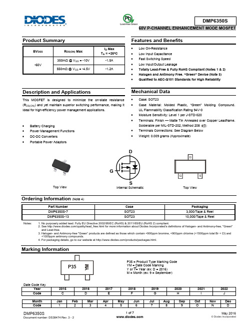
Description and ApplicationsThis MOSFET is designed to minimize the on-state resistance (R DS(ON)) and yet maintain superior switching performance, making it ideal for high-efficiency power management applications. ∙ Battery Charging∙ Power Management Functions ∙ DC-DC Converters ∙ Portable Power AdaptorsFeatures and Benefits∙ Low On-Resistance ∙ Low Input Capacitance ∙ Fast Switching Speed ∙ Low Input/Output Leakage∙ Totally Lead-Free & Fully RoHS Compliant (Notes 1 & 2) ∙ Halogen and Antimony Free. “Green” Device (Note 3) ∙Qualified to AEC-Q101 Standards for High ReliabilityMechanical Data∙ Case: SOT23∙ Case Material: Molded Plastic, “Green” Molding Compound. UL Flammability Classification Rating 94V-0 ∙ Moisture Sensitivity: Level 1 per J-STD-020∙ Terminals: Finish − Matte Tin Annealed over Copper Leadframe. Solderable per MIL-STD-202, Method 208 ∙ Terminals Connections: See Diagram Below ∙Weight: 0.009 grams (Approximate)Ordering Information (Note 4)Notes: 1. No purposely added lead. Fully EU Directive 2002/95/EC (RoHS) & 2011/65/EU (RoHS 2) compliant.2. See /quality/lead_free.html for more information about Diodes Incorporated’s definitions of Halogen - and Antimony-free, "Green" and Lead-free.3. Halogen- and Antimony-free "Green” products are defined as those which contain <900ppm bromine, <900ppm chlorine (<1500ppm total Br + Cl) and<1000ppm antimony compounds.4. For packaging details, go to our website at /products/packages.html.Marking InformationTop View Internal SchematicTop ViewP35 = Product Type Marking Code YM = Date Code Marking Y or Y= Year (ex: D = 2016) M = Month (ex: 9 = September)DSGP35Y MMaximum Ratings(@T A = +25°C unless otherwise specified.)Thermal CharacteristicsElectrical Characteristics(@T A = +25°C unless otherwise specified.)Notes: 5. Device mounted on FR-4 substrate PC board, 2oz copper, with minimum recommended pad layout.6. Device mounted on FR-4 substrate PC board, 2oz copper, with 1inch square copper plate.7. Short duration pulse test used to minimize self-heating effect.8. Guaranteed by design. Not subject to product testing.4.0-50-25 0 25 50 75 100 125 150R D S (O N ), D R A I N -S O U R C E O N -R E S I S T A N C E (Ω)T J , JUNCTION TEMPERATURE (℃)Figure 7. On-Resistance Variation with JunctionTemperaturePackage Outline DimensionsPlease see /package-outlines.html for the latest version.SOT23Suggested Pad LayoutPlease see /package-outlines.html for the latest version.SOT23All 7°。
德威特微机保护器633说明书new
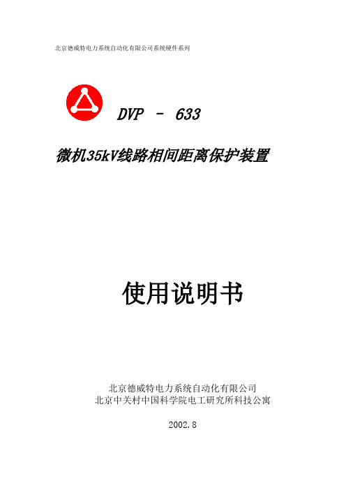
北京德威特电力系统自动化有限公司系统硬件系列DVP – 633微机35kV线路相间距离保护装置使用说明书北京德威特电力系统自动化有限公司北京中关村中国科学院电工研究所科技公寓2002.8目录1.本保护装置的适用范围 (3)2.装置的功能及特点 (3)2.1装置的主要特点 (3)2.2装置配备的保护及保护原理 (4)3.技术数据 (6)4.结构说明 (8)4.1装置组成 (8)4.2安装与开孔 (9)5.保护装置的原理图与装置端子接线说明 (9)5.1保护装置的原理图 (9)5.2装置端子图及接线说明 (10)6. 数码管的六种显示及按键的使用说明 (13)6.1数码管的六种显示 (13)6.2按键使用说明: (13)6.2.1输入密码的方法: (13)6.2.2输入修改保护定值的方法: (13)6.2.3打开与关闭保护软压板的方法: (14)6.2.4搜索的三种方法(适用于定点显示和进入定值区的显示): (14)6.3几种显示列表: (14)6.3.1正常循环显示(供运行人员使用) (14)6.3.2定点显示(供运行人员或调试人员用) (14)6.3.3定值显示修改 (16)6.3.4跳闸及报警信号指示 (17)7.调试大纲(适用于现场调试人员及检修维护人员) (17)7.1查看、输入或修改保护定值: (17)7.2开关量的检查 (17)7.3遥控分合闸继电器出口检查 (17)7.4保护继电器的出口检查 (18)7.5模拟量输入检查及精度检查 (18)7.6重合闸试验 (19)7.7距离保护试验 (19)7.8过流保护试验 (19)7.9PT回路断线报警 (20)7.10动作时间测试 (20)7.11CAN网的连接 (20)7.12.更换插件注意事项 (21)8.运行人员注意事项及要求 (21)9.检修及维护: (21)10怎样调节模拟量 (21)11.订货须知 (23)1.本保护装置的适用范围DVP-633用于35KV输电线路,完成三段式相间距离和重合闸保护功能,保护装置由监控和保护两套完全独立的系统共同构成35KV线路成套保护。
Edimax技术有限公司产品说明说明书

KEY FEATURES•802.11N High Speed: IEEE 802.11n with 300Mbps wireless speed.•Easy Installation: Ceiling-mount & T-rail mount design with easy installation kit.•Compact & Durable Housing: Ultra slim design withUL94-5VB flame-retardant plastic housing.•Multiple SSIDs for Security Management: Supports up to 16 SSIDs ideal for multiple departments, user groups, customers or guests.•Fast Roaming: Roams smoothly between APs without lag or interruption, ensuring top performance for video and voice streaming applications.•Wide Coverage & High Sensitivity: Adjustable RF output power and high receiver sensitivity for wide coverage across large spaces.•Seamless Mobility: 1.5x greater coverage than typical APs for blanket coverage to ensure seamless connectivity for Wi-Fi devices across enterprise environments.•Power over Ethernet: Supports IEEE 802.3af PoE as well as included power adapter.•Built-In RADIUS Server: With management for up to 256 user accounts.•Business Environments: Affordable choice for entry level solutions. Suitable for a wide range of commercial applications such as offices, hotels, meeting rooms, schools, campuses, resorts, retail and others.•Central Management: Edimax Pro Network Management Suite (NMS) for easy and Intuitive web-based central management. AP built-in with NMS supports AP array architecture.The CAP300-3SB is a package designed for small office and includes three CAP300 Access Points. CAP300 is a reliable and affordable entry level wireless access point designed to meet the needs of modern small to medium sized businesses, with IEEE802.11n wireless speeds up to 300Mbps. Industrial-grade performance and build quality combined with user-friendly operation, an extensive feature set and a practical, ceiling-mount design make an ideal product for day-to-day enterprise use.For businesses that demand security, flexibility and speed –the Edimax Pro series has a wide range of potential applications from office environments to schools, campuses, hotels and hospitals. Multiple SSIDs can be configured for different departments or user groups and a built-in RADIUS server provides additional verification with a scalable AP array architecture for central management of multiple access points. Fast roaming for seamless transitions between access points, Power over Ethernet support (PoE) and an intuitive web-based management interface provides flexibility for deployment and extensive management options for company MIS departments and network administrators. When performance and security are critical for your business, you need products that are engineered for your industry. The Edimax Pro series is designed to help your business and provide the connectivity that you rely on every day, with safety and effectiveness guaranteed.Affordable, Entry Level Wireless Access Point Designed For Small-to-Medium Sized BusinessesCAP300-3SB2 x 2 N Ceiling-Mount PoEAccess Point (3-Pack)SSID 1Finance Dept.SSID 2Sales Dept. SSID 3Guest RoomSSID 4 VoIPWide CoverageBYOD (Bring Your Own Device) Solution &High Density NetworkingFast RoamingHotels Offices Schools Hospitals2.4GHz2D Radiation Pattern@ HorizontalMultiple SSIDsSSID-9SSID-10SSID-11 SSID-14 SSID-15SSID-16SSID-13 SSID-12 SSID-1SSID-2 SSID-3 SSID-6SSID-7SSID-8SSID-5 SSID-4 Easy Installation KitCeiling mount and T-rail mount with bracket.2.4GHz2D Radiation Pattern@ VerticalCentral Network Management: NMSWork with Edimax Pro NMS (Network Management Suite)* web-based wireless network management software. Company MIS administrators can plan and manage Edimax Pro access points’ powerful functionalityaccording to their office space using an easy, remote web-based interface which includes a dashboard, map view, traffic statistics and wireless client list for network-wide remote administration. RADIUS settings, WLAN group settings, access control, guest network settings and firmware upgrades can all be managed centrally from a single location to reduce network downtime, aid troubleshooting and optimize network performance.Graphical zone plans with Google Maps integration and setup wizards are also available for expanding and managing large networks with multiple access points, with custom floor plans, visual overviews and easy drag-and-drop icons for quick access to key performance and monitoring information.*NMS is built-in with Edimax Pro CAP, WAP series & OAP1750 access point.Maximum performance, actual data rates, and coverage will vary depending on network conditions and environmental factors. Product specifications and design are subject to change without notice.Copyright © 2015 Edimax Technology Co. Ltd. All rights reserved.SPECIFICATIONS of CAP300 (single unit), CAP300-3SB includes 3 CAP3002 x 2 N Ceiling-Mount PoE Access PointRF SpecificationsFrequency Band •Radio Ⅰ: 802.11b/g/n 2.412~2.484(GHz)(The supported frequency band is restricted by local regulations.)Operation Channels •2.4GHz :US/Canada 1-11 / Europe 1-13 / Japan 1-14 Transmit Power(CE: 20dBm or lower, FCC:23dBm or lower)802.11b23dBm@1Mbps 23dBm@2Mbps *************23dBm@11Mbps802.11gn23dBm@6Mbps 23dBm@9Mbps 23dBm@12Mbps 23dBm@18Mbps 23dBm@24Mbps 22dBm@36Mbps 20dBm@48Mbps 19dBm@54Mbps802.11n26dBm@MCS0/MCS8 25dBm@MCS1/MCS9 25dBm@MCS2/MCS10 25dBm@MCS3/MCS11 24dBm@MCS4/MCS12 23dBm@MCS5/MCS13 22dBm@MCS6/MCS14 22dBm@MCS7/MCS15Receiver Sensitivity802.11b≤-95dBm@1Mbps ≤-90dBm@11Mbps802.11g≤-91dBm@6Mbps ≤-75dBm@54Mbps802.11n≤-93dBm@MCS0 ≤-73dBm@MCS7 ≤-90dBm@MCS8 ≤-70dBm@MCS15ManagementDeployment Standalone (AP mode)Master AP mode: Can manage 8 Edimax Pro APs with NMSManaged AP mode : Be managed by AP Controller (APC500), Edimax Pro Master AP with NMS softwareConfigurationHTTP/HTTPS SNMP v1, v2c, v3 CLI (Telnet, SSH)RADIUS Server Built-In Auto-Channel Y Private MIB YPackage Contents Access Point N300 Ceiling Mount PoE Access Point Mounting Bracket Ceiling-Mount & T-rail Mount Bracket KitPower Adapter 12V / 1A Power AdapterCableEthernet CableCD / Quick Installation Guide CD (User Manual & Multi-Language Quick Installation Guide) / Printed English QuickInstallation GuideAccessories OptionalGP-101IT IEEE802.3at PoE InjectorHardware LAN Interface Giga x 1PoE 802.3af (Supports 802.3at)Antenna Type: 2 x Built-In PIFA / Gain: 2.82dBi Max.Power DC: 12V / 1A802.3af (PoE Injector Optional)Dimensions 17.6 (D) x 3.2 (H) cmWeight287.3g Power Consumption (Full Loading) 6.5W Mounting CeilingReset YLED Indicator 1. Power LED 2. Diag LEDEnvironmental Conditions Operating Temperature: 0°C (32°F) to 50°C (122°F) Storage Temperature : -20°C (-4°F) to 60°C (140°F)Operating Humidity: 90% or Less Storage Humidity: 90% or LessPower Saving 802.3azInternal Buzzer YHousing UL94-5VB Flammability RatingWireless Standard 802.11 b/g/nNo. of Radios 1 Receiver Sensitivity ≤ -95dBm Certification CE/FCCFast Roaming Y Number of SSIDs 16 Performance Maximum Data Speed300Mbps Concurrent Clients Up to 50* Per RadioSecurity EncryptionWEP / WPA / WPA2Wireless L2 Isolation Y Station Isolation Y IEEE 802.1x AuthenticatorY EAP Authentication PEAP Hidden SSID Y MAC Address Filter Y Wireless STAY Rogue AP Detection (w/ NMS) YSoftware Wireless Mode AP / WDS AP / WDS Bridge802.1q VLAN Y (VID = 1-4095)Spanning Tree RSTP QoSWMM (802.11e) Max Associated Station No. Pass-Through IPv6 and VPN (PPTP, L2TP/IPsec)DSCP (802.1p)Y Multicast Rate up to 54MbpsY12V DC Power PortLAN Port with PoE INStatus LED Reset Button*The maximum users in 2.4GHz is depends on the interference condition of the environment.。
MAXIM 化数字电位器MAX5481, MAX5482, MAX5483, MAX548 说明书

ENGLISH•简体中文•日本語•概述状况状况:生产中。
下载Notes MAX5481Linear13-WireSerial SPINon-Volatile102410253519.6$1.95@1kMAX548250$1.95 @1kMAX548310$1.95 @1kMAX548450$1.95 @1k查看所有Digital Potentiometers (128)引脚配置相关产品MAX5494,MAX5495,MAX5496, ...10位、双路、非易失、线性变化数字电位器类似产品:浏览其它类似产品线查看所有Digital Potentiometers (128产品)顶标MAX5481顶标MAX5482顶标MAX5483顶标MAX5484新品发布[ 2005-08-03 ]应用工程师帮助选型,下个工作日回复参数搜索应用帮助概述技术文档定购信息概述关键特性应用/使用关键指标图表注释、注解相关产品数据资料应用笔记评估板设计指南可靠性报告软件/模型价格与供货样品在线订购封装信息无铅信息参考文献: 19-3708 Rev. 4; 2008-03-12本页最后一次更新: 2008-03-27联络我们:信息反馈、提出问题 • 对该网页的评价 • 发送本网页 • 隐私权政策 • 法律声明 © 2010 Maxim Integrated Products版权所有General DescriptionThe MAX5481–MAX5484 10-bit (1024-tap) nonvolatile,linear-taper, programmable voltage-dividers and vari-able resistors perform the function of a mechanical potentiometer, but replace the mechanics with a pin-configurable 3-wire serial SPI™-compatible interface or up/down digital interface. The MAX5481/MAX5482 are 3-terminal voltage-dividers and the MAX5483/MAX5484are 2-terminal variable resistors.The MAX5481–MAX5484 feature an internal, non-volatile, electrically erasable programmable read-only memory (EEPROM) that stores the wiper position for ini-tialization during power-up. The 3-wire SPI-compatible serial interface allows communication at data rates up to 7MHz. A pin-selectable up/down digital interface is also available.The MAX5481–MAX5484 are ideal for applications requiring digitally controlled potentiometers. Two end-to-end resistance values are available (10k Ωand 50k Ω) in a voltage-divider or a variable-resistor configuration (see the Selector G uide ). The nominal resistor temperature coefficient is 35ppm/°C end-to-end, and only 5ppm/°C ratiometric, making these devices ideal for applications requiring low-temperature-coefficient voltage-dividers,such as low-drift, programmable gain-amplifiers.The MAX5481–MAX5484 operate with either a +2.7V to +5.25V single power supply or ±2.5V dual power sup-plies. These devices consume 400µA (max) of supply current when writing data to the nonvolatile memory and 1.0µA (max) of standby supply current. The MAX5481–MAX5484 are available in a space-saving (3mm x 3mm), 16-pin TQFN, or a 14-pin TSSOP pack-age and are specified over the extended (-40°C to +85°C) temperature range.ApplicationsFeatures♦1024 Tap Positions♦Power-On Recall of Wiper Position from Nonvolatile Memory♦16-Pin (3mm x 3mm x 0.8mm) TQFN or 14-Pin TSSOP Package♦35ppm/°C End-to-End Resistance Temperature Coefficient♦5ppm/°C Ratiometric Temperature Coefficient ♦10kΩand 50kΩEnd-to-End Resistor Values♦Pin-Selectable SPI-Compatible Serial Interface or Up/Down Digital Interface ♦1µA (max) Standby Current♦Single +2.7V to +5.25V Supply Operation ♦Dual ±2.5V Supply OperationMAX5481–MAX548410-Bit, Nonvolatile, Linear-Taper DigitalPotentiometers________________________________________________________________Maxim Integrated Products1Ordering InformationPin Configurations19-3708; Rev 5; 4/10For pricing delivery, and ordering information please contact Maxim Direct at 1-888-629-4642,or visit Maxim’s website at .Selector Guide appears at end of data sheet.SPI is a trademark of Motorola, Inc.temperature range.+Denotes a lead(Pb)-free/RoHS-compliant package.*EP = Exposed pad.Ordering Information continued at end of data sheet.Gain and Offset AdjustmentLCD Contrast Adjustment Pressure SensorsLow-Drift Programmable Gain AmplifiersMechanical Potentiometer ReplacementM A X 5481–M A X 548410-Bit, Nonvolatile, Linear-Taper Digital PotentiometersABSOLUTE MAXIMUM RATINGSStresses beyond those listed under “Absolute Maximum Ratings” may cause permanent damage to the device. These are stress ratings only, and functional operation of the device at these or any other conditions beyond those indicated in the operational sections of the specifications is not implied. Exposure to absolute maximum rating conditions for extended periods may affect device reliability.V DD to GND...........................................................-0.3V to +6.0V V SS to GND............................................................-3.5V to +0.3V V DD to V SS .............................................................-0.3V to +6.0V H, L, W to V SS ..................................(V SS - 0.3V) to (V DD + 0.3V)CS , SCLK(INC ), DIN(U/D ), SPI/UD to GND..-0.3V to (V DD + 0.3V)Maximum Continuous Current into H, L, and WMAX5481/MAX5483.........................................................±5mA MAX5482/MAX5484......................................................±1.0mA Maximum Current into Any Other Pin...............................±50mAContinuous Power Dissipation (T A = +70°C)16-Pin TQFN (derate 17.5mW/°C above +70°C).....1398.6mW 14-Pin TSSOP (derate 9.1mW/°C above +70°C)..........727mW Operating Temperature Range ...........................-40°C to +85°C Junction Temperature......................................................+150°C Storage Temperature Range.............................-60°C to +150°C Lead Temperature (soldering, 10s).................................+300°C Soldering Temperature (reflow).......................................+260°CELECTRICAL CHARACTERISTICSMAX5481–MAX548410-Bit, Nonvolatile, Linear-Taper DigitalPotentiometers_______________________________________________________________________________________3ELECTRICAL CHARACTERISTICS (continued)(V DD = +2.7V to +5.25V, V SS = V GND = 0V, V H = V DD , V L = 0V, T A = -40°C to +85°C, unless otherwise noted. Typical values are at V DD = +5.0V, T A = +25°C, unless otherwise noted.) (Note 1)M A X 5481–M A X 548410-Bit, Nonvolatile, Linear-Taper Digital Potentiometers 4_______________________________________________________________________________________TIMING CHARACTERISTICSNote 2:The DNL and INL are measured with the device configured as a voltage-divider with H = V DD and L = V SS . The wiper termi-nal (W) is unloaded and measured with a high-input-impedance voltmeter.Note 3:The DNL_R and INL_R are measured with D.N.C. unconnected and L = V SS = 0V. For V DD = +5V, the wiper terminal is dri-ven with a source current of I W = 80µA for the 50k Ωdevice and 400µA for the 10k Ωdevice. For V DD = +3V, the wiper termi-nal is driven with a source current of 40µA for the 50k Ωdevice and 200µA for the 10k Ωdevice.Note 4:The wiper resistance is measured using the source currents given in Note 3.Note 5:The device draws higher supply current when the digital inputs are driven with voltages between (V DD - 0.5V) and (V GND +0.5V). See Supply Current vs. Digital Input Voltage in the Typical Operating Characteristics .Note 6:Wiper settling test condition uses the voltage-divider configuration with a 10pF load on W. Transition code from 00000 00000to 01111 01111 and measure the time from CS going high to the wiper voltage settling to within 0.5% of its final value.MAX5481–MAX548410-Bit, Nonvolatile, Linear-Taper DigitalPotentiometers_______________________________________________________________________________________5-1.0-0.6-0.8-0.2-0.40.200.40.80.61.002563841285126407688961024DNL vs. CODE (MAX5483)CODED N L (L S B )V DD = 2.7V-1.0-0.6-0.8-0.2-0.40.200.40.80.61.002563841285126407688961024DNL vs. CODE (MAX5483)CODED N L (L S B )V DD = 5V-2.0-1.0-1.50-0.50.51.01.5 2.0INL vs. CODE (MAX5483)I N L (L S B )V DD = 2.7V02563841285126407688961024CODE-2.0-1.0-1.50-0.50.51.01.5 2.0INL vs. CODE (MAX5483)I N L (L S B )V DD = 3V2563841285126407688961024CODE-2.0-1.0-1.50-0.50.51.01.5 2.0INL vs. CODE (MAX5483)I N L (L S B )V DD = 5V02563841285126407688961024CODE-1.0-0.6-0.8-0.2-0.40.200.40.80.61.002563841285126407688961024DNL vs. CODE (MAX5481)CODED N L (L S B )-1.0-0.6-0.8-0.2-0.40.200.40.80.61.002563841285126407688961024DNL vs. CODE (MAX5481)CODED N L (L S B )V DD = 5V-1.0-0.6-0.8-0.2-0.40.200.40.80.61.002563841285126407688961024INL vs. CODE (MAX5481)CODEI N L (L S B )-1.0-0.6-0.8-0.2-0.40.200.40.80.61.002563841285126407688961024INL vs. CODE (MAX5481)CODEI N L (L S B )Typical Operating Characteristics(V DD = 5.0V, V SS = 0V, T A = +25°C, unless otherwise noted.)M A X 5481–M A X 548410-Bit, Nonvolatile, Linear-Taper Digital Potentiometers 6_______________________________________________________________________________________-1.0-0.6-0.8-0.2-0.40.200.40.80.61.002563841285126407688961024DNL vs. CODE (MAX5484)CODED N L (L S B )-1.0-0.6-0.8-0.2-0.40.200.40.80.61.002563841285126407688961024DNL vs. CODE (MAX5484)CODED N L (L S B )-1.0-0.6-0.8-0.2-0.40.200.40.80.61.002563841285126407688961024INL vs. CODE (MAX5484)CODEI N L (L S B )-1.0-0.6-0.8-0.2-0.40.200.40.80.61.002563841285126407688961024INL vs. CODE (MAX5484)CODEI N L (L S B )-1.0-0.6-0.8-0.2-0.40.200.40.80.61.002563841285126407688961024DNL vs. CODE (MAX5482)CODED N L (L S B )-1.0-0.6-0.8-0.2-0.40.200.40.80.61.002563841285126407688961024DNL vs. CODE (MAX5482)CODED N L (L S B )-1.0-0.6-0.8-0.2-0.40.200.40.80.61.002563841285126407688961024INL vs. CODE (MAX5482)CODEI N L (L S B )V DD = 2.7V-1.0-0.6-0.8-0.2-0.40.200.40.80.61.02563841285126407688961024INL vs. CODE (MAX5482)CODEI N L (L S B )V DD = 5V02010403050607080WIPER RESISTANCE vs. CODE (VARIABLE RESISTOR, T A = -40°C)M A X 5481 t o c 18R W (Ω)2563841285126407688961024CODETypical Operating Characteristics (continued)(V DD = 5.0V, V SS = 0V, T A = +25°C, unless otherwise noted.)MAX5481–MAX5484Typical Operating Characteristics (continued)(V DD = 5.0V, V SS = 0V, T A = +25°C, unless otherwise noted.)10-Bit, Nonvolatile, Linear-Taper DigitalPotentiometers_______________________________________________________________________________________702010403050607080WIPER RESISTANCE vs. CODE (VARIABLE RESISTOR, T A = +25°C)M A X 5481 t oc 19R W (Ω)2563841285126407688961024CODE2010403050607080WIPER RESISTANCE vs. CODE (VARIABLE RESISTOR, T A = +85°C)M A X 5481 t o c 20R W (Ω)2563841285126407688961024CODE10302050604070W-TO-L RESISTANCE vs. CODE(MAX5484)R W L (k Ω)02563841285126407688961024CODE02641012814W-TO-L RESISTANCE vs. CODE(MAX5483)R W L (k Ω)2563841285126407688961024CODE18.018.519.019.520.020.521.021.522.0012345WIPER RESISTANCE vs. WIPER VOLTAGE(VARIABLE RESISTOR)WIPER VOLTAGE (V)R W (Ω)-2.0-1.5-1.0-0.500.51.01.52.0-40-1510356085END-TO-END (R HL ) % CHANGE vs. TEMPERATURE (VOLTAGE-DIVIDER)M A X 5481 t o c 24TEMPERATURE (°C)E N D -T O -E N D R E S I S T A N C E C H A N G E (%)-2.0-1.5-1.0-0.500.51.01.52.0-40-1510356085WIPER-TO-END RESISTANCE (R WL ) % CHANGE vs. TEMPERATURE (VARIABLE RESISTOR)TEMPERATURE (°C)W I P E R -T O -E N D R E S I S T A N C E C H A N G E (%)00.30.90.61.21.5-4010-15356085STANDBY SUPPLY CURRENTvs. TEMPERATURETEMPERATURE (°C)I D D (μA )DIGITAL SUPPLY CURRENT vs. DIGITAL INPUT VOLTAGEDIGITAL INPUT VOLTAGE (V)I D D (μA )4.54.03.53.02.52.01.51.00.5110100100010,0000.15.0M A X 5481–M A X 548410-Bit, Nonvolatile, Linear-Taper Digital Potentiometers Typical Operating Characteristics (continued)(Circuit of Figure 1, T A = +25°C, unless otherwise noted.)1μs/divTAP-TO-TAP SWITCHING TRANSIENTRESPONSE (MAX5481)V W(AC-COUPLED)20mV/divCS 2V/divH = V DD , L = GND C W = 10pFFROM CODE 01 1111 1111TO CODE 10 0000 00004μs/divTAP-TO-TAP SWITCHING TRANSIENTRESPONSE (MAX5482)V W(AC-COUPLED)20mV/divCS 2V/divH = V DD , L = GND C W = 10pFFROM CODE 01 1111 1111TO CODE 10 0000 0000WIPER RESPONSE vs. FREQUENCY(MAX5481)FREQUENCY (kHz)G A I N (d B )100101-20-15-10-5-250.11000WIPER RESPONSE vs. FREQUENCY(MAX5482)FREQUENCY (kHz)G A I N (d B )100101-20-15-10-50-250.11000THD+N vs. FREQUENCY(MAX5481)FREQUENCY (kHz)T H D +N (%)1010.10.0010.010.11100.00010.01100THD+N vs. FREQUENCY(MAX5482)FREQUENCY (kHz)T H D +N (%)1010.10.0010.010.11100.00010.0110004020806012010014018016020002563841285126407688961024RATIOMETRIC TEMPERATURE COEFFICIENT vs. CODECODER A T I O M E T R I C T E M P C O (p p m )100300200500600400700VARIABLE-RESISTOR TEMPERATURECOEFFICIENT vs. CODET C V R (p p m )02563841285126407688961024CODE10-Bit, Nonvolatile, Linear-Taper DigitalPotentiometersPin DescriptionMAX5481–MAX5484M A X 5481–M A X 548410-Bit, Nonvolatile, Linear-Taper Digital Potentiometers Pin Description (continued)(MAX5483/MAX5484 Variable Resistors)MAX5481–MAX548410-Bit, Nonvolatile, Linear-Taper DigitalPotentiometersFunctional DiagramsM A X 5481–M A X 548410-Bit, Nonvolatile, Linear-Taper Digital Potentiometers Detailed DescriptionThe MAX5481/MAX5482 linear programmable voltage-dividers and the MAX5483/MAX5484 variable resistors feature 1024 tap points (10-bit resolution) (see the Functional Diagrams ). These devices consist of multi-ple strings of equal resistor segments with a wiper con-tact that moves among the 1024 points through a pin-selectable 3-wire SPI-compatible serial interface or up/down interface. The MAX5481/MAX5483 provide a total end-to-end resistance of 10k Ω, and the MAX5482/MAX5484 have an end-to-end resistance of 50k Ω. The MAX5481/MAX5482 allow access to the high, low, and wiper terminals for a standard voltage-divider configuration.MAX5481/MAX5482 ProgrammableVoltage-DividersThe MAX5481/MAX5482 programmable voltage-dividers provide a weighted average of the voltage between the H and L inputs at the W output. Both devices feature 10-bit resolution and provide up to 1024 tap points between the H and L voltages. Ideally,the V L voltage occurs at the wiper terminal (W) when all data bits are zero and the V H voltage occurs at the wiper terminal when all data bits are one. The step size (1 LSB) voltage is equal to the voltage applied across terminals H and L divided by 210. Calculate the wiper voltage V Was follows:Functional Diagrams (continued)MAX5481–MAX548410-Bit, Nonvolatile, Linear-Taper DigitalPotentiometerswhere D is the decimal equivalent of the 10 data bits writ-ten (0 to 1023), V HL is the voltage difference between the H and L terminals:The MAX5481 includes a total end-to-end resistance value of 10k Ωwhile the MAX5482 features an end-to-end resistance value of 50k Ω. These devices are not intended to be used as a variable resistor . Wiper cur-rent creates a nonlinear voltage drop in series with the wiper. To ensure temperature drift remains within speci-fications, do not pull current through the voltage-divider wiper. Connect the wiper to a high-impedance node.Figures 1 and 2 show the behavior of the MAX5481’s resistance from W to H and from W to L. This does not apply to the variable-resistor devicesMAX5483/MAX5484 Variable ResistorsThe MAX5483/MAX5484 provide a programmable resistance between W and L. The MAX5483 features a total end-to-end resistance value of 10k Ω, while the MAX5484 provides an end-to-end resistance value of 50k Ω. The programmable resolution of this resistance is equal to the nominal end-to-end resistance divided by 1024 (10-bit resolution). For example, each nominal segment resistance is 9.8Ωand 48.8Ωfor the MAX5483and the MAX5484, respectively.wiper position from the 1024 possible positions, result-ing in 1024 values for the resistance from W to L.Calculate the resistance from W to L (R WL ) by using the where D is decimal equivalent of the 10 data bits writ-ten, R W-L is the nominal end-to-end resistance, and R Z is the zero-scale error. Table 1 shows the values of R WL at selected codes for the MAX5483/MAX5484.Digital InterfaceConfigure the MAX5481–MAX5484 by a pin-selectable,3-wire, SPI-compatible serial data interface or an up/down interface. Drive SPI/UD high to select the 3-wire SPI-compatible interface. Pull SPI/UD low to select the up/down interface.V FSE V andV ZSE V FSE HL ZSE HL =⎡⎣⎢⎤⎦⎥=⎡⎣⎢⎤⎦⎥10241024,Figure 1. Resistance from W to H vs. Code (10k ΩVoltage-Divider)Figure 2. Resistance from W to L vs. Code (10k ΩVoltage-Divider)M A X 5481–M A X 548410-Bit, Nonvolatile, Linear-Taper Digital Potentiometers SPI-Compatible Serial InterfaceDrive SPI/UD high to enable the 3-wire SPI-compatible serial interface (see Figure 3). This write-only interface contains three inputs: chip select (CS ), data in (DIN(U/D )), and data clock (SCLK(INC )). Drive CS low to load the data at DIN(U/D ) synchronously into the shift register on each SCLK(INC ) rising edge.The WRITE command (C1, C0 = 00) requires 24 clock cycles to transfer the command and data (Figure 4a).The COPY commands (C1, C0 = 10 or 11) use either eight clock cycles to transfer the command bits (Figure 4b) or 24 clock cycles with the last 16 data bits disre-garded by the device.After loading the data into the shift register, drive CS high to latch the data into the appropriate control regis-ter. Keep CS low during the entire serial data stream to avoid corruption of the data. Table 2 shows the com-mand decoding.Write Wiper RegisterData written to this register (C1, C0 = 00) controls the wiper position. The 10 data bits (D9–D0) indicate the position of the wiper. For example, if DIN(U/D ) = 00 00000000, the wiper moves to the position closest to L. If DIN(U/D ) = 11 1111 1111, the wiper moves closest to H.This command writes data to the volatile random access memory (RAM), leaving the NV register unchanged. When the device powers up, the data stored in the NV register transfers to the wiper register,moving the wiper to the stored position. Figure 5 shows how to write data to the wiper register.Table 2. Command Decoding*X = Don’t care.Figure 3. SPI-Compatible Serial-Interface Timing Diagram (SPI/UD = 1)10-Bit, Nonvolatile, Linear-Taper DigitalPotentiometers ArrayMAX5481–MAX5484Figure4. Serial SPI-Compatible Interface FormatFigure5. Write Wiper Register OperationM A X 5481–M A X 548410-Bit, Nonvolatile, Linear-Taper Digital Potentiometers Copy Wiper Register to NV RegisterThe copy wiper register to NV register command (C1,C0 = 10) stores the current position of the wiper to the NV register for use at power-up. Figure 6 shows how to copy data from wiper register to NV register. The oper-ation takes up to 12ms (max) after CS goes high to complete and no other operation should be performed until completion.Copy NV Register to Wiper RegisterThe copy NV register to wiper register (C1, C0 = 11)restores the wiper position to the current value stored in the NV register. Figure 7 shows how to copy data from the NV register to the wiper register.Digital Up/Down InterfaceFigure 8 illustrates an up/down serial-interface timing diagram. In digital up/down interface mode (SPI/UD =0), the logic inputs CS , DIN(U/D ), and SCLK(INC ) con-trol the wiper position and store it in nonvolatile memory (see Table 3). The chip-select (CS ) input enables the serial interface when low and disables the interface when high. The position of the wiper is stored in the nonvolatile register when CS transitions from low to high while SCLK(INC ) is high.When the serial interface is active (CS low), a high-to-low (falling edge) transition on SCLK(INC ) increments or decrements the internal 10-bit counter depending on the state of DIN(U/D ). If DIN(U/D ) is high, the wiper increments. If DIN(U/D ) is low, the wiper decrements.The device stores the value of the wiper position in the nonvolatile memory when CS transitions from low to high while SCLK(INC ) is high. The host system can disablethe serial interface and deselect the device without stor-ing the latest wiper position in the nonvolatile memory by keeping SCLK(INC ) low while taking CS high.Upon power-up, the MAX5481–MAX5484 load the value of nonvolatile memory into the wiper register, and set the wiper position to the value last stored.Figure 6. Copy Wiper Register to NV Register OperationFigure 7. Copy NV Register to Wiper Register OperationMAX5481–MAX548410-Bit, Nonvolatile, Linear-Taper DigitalPotentiometersStandby ModeThe MAX5481–MAX5484 feature a low-power standby mode. When the device is not being programmed, it enters into standby mode and supply current drops to 0.5µA (typ).Nonvolatile MemoryThe internal EEPROM consists of a nonvolatile register that retains the last value stored prior to power-down.The nonvolatile register is programmed to midscale at the factory. The nonvolatile memory is guaranteed for 50 years of wiper data retention and up to 200,000wiper write cycles.Power-UpUpon power-up, the MAX5481–MAX5484 load the data stored in the nonvolatile wiper register into the volatile wiper register, updating the wiper position with the data stored in the nonvolatile wiper register.Applications InformationThe MAX5481–MAX5484 are ideal for circuits requiring digitally controlled adjustable resistance, such as LCD contrast control (where voltage biasing adjusts the dis-play contrast), or programmable filters with adjustable gain and/or cutoff frequency.Positive LCD Bias ControlFigures 9 and 10 show an application where a voltage-divider or a variable resistor is used to make an adjustable, positive LCD-bias voltage. The op amp pro-vides buffering and gain to the voltage-divider network made by the programmable voltage-divider (Figure 9) or to a fixed resistor and a variable resistor (see Figure 10).Programmable Gain and Offset AdjustmentFigure 11 shows an application where a voltage-divider and a variable resistor are used to make a programma-ble gain and offset adjustment.Figure 8. Up/Down Serial-Interface Timing Diagram (SPI/UD = 0)M A X 5481–M A X 548410-Bit, Nonvolatile, Linear-Taper Digital Potentiometers 18______________________________________________________________________________________Programmable FilterFigure 12 shows the configuration for a 1st-order pro-grammable filter using two variable resistors. Adjust R2for the gain and adjust R3 for the cutoff frequency. Use the following equations to estimate the gain (G) and the 3dB cutoff frequency (f C):Figure 10. Positive LCD Bias Control Using a Variable ResistorFigure 12. Programmable FilterFigure 11. Programmable Gain/Offset AdjustmentFigure 9. Positive LCD Bias Control Using a Voltage-DividerMAX5481–MAX548410-Bit, Nonvolatile, Linear-Taper DigitalPotentiometers______________________________________________________________________________________19Chip InformationPROCESS: BiCMOSSelector GuidePin Configurations (continued)Ordering Information (continued)Note: All devices are specified over the -40°C to +85°C operating temperature range.+Denotes a lead(Pb)-free/RoHS-compliant package.*EP = Exposed pad.Package InformationFor the latest package outline information and land patterns, go to /packages . Note that a “+”, “#”, or “-” in the package code indicates RoHS status only. Package draw-ings may show a different suffix character, but the drawing per-tains to the package regardless of RoHS status.M A X 5481–M A X 548410-Bit, Nonvolatile, Linear-Taper Digital Potentiometers Maxim cannot assume responsibility for use of any circuitry other than circuitry entirely embodied in a Maxim product. No circuit patent licenses are implied. Maxim reserves the right to change the circuitry and specifications without notice at any time.20____________________Maxim Integrated Products, 120 San Gabriel Drive, Sunnyvale, CA 94086 408-737-7600©2010 Maxim Integrated ProductsMaxim is a registered trademark of Maxim Integrated Products, Inc.。
6m33d633e200技术参数
6m33d633e200技术参数6m33d633e200是一款先进的技术设备,广泛应用于各个行业。
本文将重点介绍6m33d633e200的技术参数,以便更好地了解和使用该设备。
1. 尺寸与重量:- 6m33d633e200的尺寸为X厘米(长)×Y厘米(宽)×Z厘米(高)。
- 6m33d633e200的重量约为W千克。
2. 处理器:- 6m33d633e200采用先进的处理器技术,具有高性能和低能耗的特点。
- 处理器速度为S GHz,能够快速处理各种任务和数据。
3. 存储容量:- 6m33d633e200拥有大容量的内部存储空间,可用于存储大量数据和文件。
- 内部存储容量为C GB,足够满足日常使用的需求。
4. 内存:- 6m33d633e200配备了高速的内存,能够提供流畅且高效的操作体验。
- 内存容量为M GB,能够支持同时运行多个应用程序和任务。
5. 屏幕:- 6m33d633e200配备了高分辨率的液晶显示屏,能够呈现清晰、鲜艳的图像和视频。
- 屏幕尺寸为P英寸,具有宽广的视野和舒适的观看体验。
6. 摄像头:- 6m33d633e200内置了高像素的摄像头,能够拍摄出高质量的照片和视频。
- 摄像头像素为A万像素,支持自动对焦和光学防抖功能。
7. 电池续航:- 6m33d633e200搭载了容量较大的电池,能够提供长时间的使用时间。
- 电池续航时间约为B小时,可满足一天的正常使用需求。
8. 网络与连接:- 6m33d633e200支持多种网络连接方式,如Wi-Fi、蓝牙等。
- 支持的网络频段为X GHz至Y GHz,确保稳定的网络连接。
9. 操作系统:- 6m33d633e200采用先进的操作系统,提供丰富的功能和良好的用户体验。
- 操作系统版本为Z,具有稳定性和安全性。
10. 其他功能:- 6m33d633e200还具有其他一些特殊功能,如指纹识别、面部识别等,提供更高的安全性和便利性。
MEMORY存储芯片MAX3232ESE中文规格书
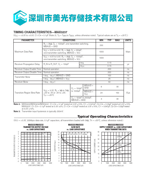
__________________________________________Typical Operating Characteristics(V CC = +3.3V, 235kbps data rate, 0.1µF capacitors, all transmitters loaded with 3k Ω, T A = +25°C, unless otherwise noted.)TIMING CHARACTERISTICS—MAX3237(V CC = +3.0V to +5.5V, C1–C4 = 0.1µF (Note 2), T A = T MIN to T MAX , unless otherwise noted. Typical values are at T A = +25°C.)Note 2:MAX3222/MAX3232/MAX3241: C1–C4 = 0.1µF tested at 3.3V ±10%; C1 = 0.047µF, C2–C4 = 0.33µF tested at 5.0V ±10%.MAX3237: C1–C4 = 0.1µF tested at 3.3V ±5%; C1–C4 = 0.22µF tested at 3.3V ±10%; C1 = 0.047µF, C2–C4 = 0.33µF tested at 5.0V ±10%.Note 3:Transmitter input hysteresis is typically 250mV.-6-5-4-3-2-101234560MAX3222/MAX3232TRANSMITTER OUTPUT VOLTAGEvs. LOAD CAPACITANCELOAD CAPACITANCE (pF)T R A N S M I T T E R O U T P U T V O L T A G E (V )20003000100040005000246810121416182022150MAX3222/MAX3232SLEW RATEvs. LOAD CAPACITANCELOAD CAPACITANCE (pF)S L E W R A T E (V /μs )20003000100040005000510152025303540MAX3222/MAX3232SUPPLY CURRENT vs. LOAD CAPACITANCEWHEN TRANSMITTING DATALOAD CAPACITANCE (pF)S U P P L Y C U R R E N T (m A )20003000100040005000MAX3222/MAX3232/MAX3237/MAX32413.0V to 5.5V, Low-Power, up to 1Mbps, True RS-232 Transceivers Using Four 0.1µF External CapacitorsFigure 4a. MAX3241 Transmitter Output Voltage vs. Load Current per Transmitter3.0V to 5.5V , Low-Power, up to 1Mbps, True RS-232Transceivers Using Four 0.1µF External CapacitorsMAX3222/MAX3232/MAX3237/MAX3241CC = 3.3V5μs/divFigure 5. Loopback Test CircuitHigh Data RatesThe MAX3222/MAX3232/MAX3241 maintain the RS-232±5.0V minimum transmitter output voltage even at high data rates. Figure 5 shows a transmitter loopb ack test circuit. Figure 6 shows a loopb ack test result at 120kbps, and Figure 7 shows the same test at 235kbps. For Figure 6, all transmitters were driven simultaneously at 120kb ps into RS-232 loads in parallel with 1000pF. For Figure 7, a single transmitter was driven at 235kbps, and all transmitters were loaded with an RS-232 receiver in parallel with 1000pF.The MAX3237 maintains the RS-232 ±5.0V minimum transmitter output voltage at data rates up to 1Mb ps. Figure 8 shows a loopb ack test result at 1Mb ps with MBAUD = V CC . For Figure 8, all transmitters were loaded with an RS-232 receiver in parallel with 250pF.fdzfdfbbFigure 6. MAX3241 Loopback Test Result at 120kbpsCC = 3.3V2μs/divFigure 7. MAX3241 Loopback Test Result at 235kbps0V +5V 0V -5V +5V 0VT_INT_OUT = R_IN 5k R_OUT 150pF200ns/divCC = 3.3VFigure 8. MAX3237 Loopback Test Result at 1000kbps (MBAUD = V CC )___________________Chip Topography___________________Chip InformationT1INT2IN 0.087"(2.209mm)R2OUTR2IN T2OUT R1OUTR1INT1OUTV CCV+C1+ENC1-C2+C2-V-GNDTRANSISTOR COUNT: 339SUBSTRATE CONNECTED TO GNDMAX3222/MAX3232/MAX3237/MAX3241 3.0V to 5.5V, Low-Power, up to 1Mbps, True RS-232Transceivers Using Four 0.1µF External Capacitors。
MAX4173

高端电流检测放大器性能分析在讨论器件功能时,检流放大器可以看作一个输入级浮空的仪表/差分放大器。
这意味着即使器件采用VCC=3.3V或5V单电源供电,在输入共模电压远高于电源电压的条件下,器件仍然能够正常放大差分输入信号。
检流放大器的共模电压可以很高,例如可以高达28V(MAX4372和MAX4173)或76V(MAX4080和MAX4081)。
检流放大器的这一特性使其非常适合高端电流检测应用,这类应用往往需要对高压侧检流电阻两端的微小电压进行放大,并馈入到低压ADC或低压模拟控制环路进行处理。
这种情况下,通常需要在信号源端(例如检流电阻两端)对电流检测信号进行滤波。
可以采用差分滤波器(图1)滤除负载电流和检流电压的“毛刺”,也可以采用共模滤波器(图2)以增强在出现共模电压尖峰或瞬时过压时的ESD保护能力。
合理选择元件构建滤波器,如果元件选择不当,则会引入一些无法预知的失调电压和增益误差,降低电路性能。
滤波器的选择MAX4173检流放大器如图3所示,该器件的检流电阻可直接连接到芯片的RS+和RS-端。
器件内部的运算放大器将检流电阻两端的差分电压恢复成RG1两端的差分电压,即ILOAD×RSENSE=VSENSE=IRG1×RG1。
然后,内部电流镜对电流IRG1进行电平转换和放大,产生输出电流IRGD。
MAX4173的内部电路中RGD=12kΩ,而RG1=6kΩ。
因此,由于RGD和RG1为片上电阻,实际阻值会因不同的半导体工艺而产生多达±30%的差异。
但是,因为最终增益精度取决于RGD和RG1的比例,所以可以很好地控制增益,并在生产过程中灵活调整。
构建差分/共模滤波器(如图1和图2所示)时,需要在检流电阻的RSENSE+和RSENSE-端与器件的RS+和RS-引脚之间接入串联电阻,此时相当于改变了芯片的RG1和RG2。
由上面的等式可知,改变后的RG1将引入增益误差。
同时,由于RG1的绝对误差最大可达±30%,因此增益误差最大将达到±30%,由于这种误差的引入是随机的,所以无法控制或估算误差。
MAX5438 数字电位器

General DescriptionThe MAX5436–MAX5439 are 128-tap high-voltage (±5V to ±15V) digital potentiometers in packages that are half the size of comparable devices in 8-pin SO. They perform the same function as mechanical potentiometers, but replace the mechanics with a simple digital interface. The digital logic is powered by a separate single +2.7V to +5.25V supply voltage (V CC ). The resistor string uses its own analog supplies (V DD and V SS ) that require V DD - V SS to be greater than 9V and less than 31.5V. This allows for greater flexibility in voltage ranges that can be used with these devices. Examples of analog supply ranges include not only dual voltages of ±5V to ±15V, but single-supply voltages, such as +10V, +15V, +30V, -30V,and more, as long as the ranges of V DD - V SS and V CC -V SS are met.The MAX5437/MAX5439 include an on-chip, high-voltage, uncommitted amplifier, providing additional reductions in board space and cost. Other features include low 35ppm/°C end-to-end and 5ppm/°C ratio-metric resistor temperature coefficients, a 3-wire SPI™/QSPI™/MICROWIRE™-compatible serial interface, and a power-on reset to midscale.The MAX5436/MAX5438 are available in 10-pin µMAX packages. The MAX5437/MAX5439 are available in 14-pin TSSOP package. Each device is guaranteed over the extended temperature range of -40°C to +85°C.ApplicationsLCD Screen Contrast Adjustment Data-Acquisition SystemsMechanical Potentiometer Replacement Low-Drift Programmable Gain Amplifier Audio Volume ControlFeatures♦+10V to +30V Single-Supply Operation ♦-28V to -10V Single Negative Supply Operation ♦±5V to ±15V Dual-Supply Operation ♦128 Tap Positions♦Uncommitted High-Voltage Amplifier (MAX5437/MAX5439)♦Low Temperature Coefficient 35ppm/°C (End-to-End) 5ppm/°C (Ratiometric)♦Small-Footprint Packages10-Pin µMAX (MAX5436/MAX5438)14-Pin TSSOP (MAX5437/MAX5439)♦Glitchless Switching Between the Resistor Taps ♦3-Wire SPI/QSPI/MICROWIRE-Compatible Serial Interface ♦50k Ω/100k ΩEnd-to-End Resistances ♦Power-On Reset: Wiper Goes to Midscale (Position 64)MAX5436–MAX5439±15V , 128-Tap, Low-Drift Digital Potentiometers________________________________________________________________Maxim Integrated Products 1Pin ConfigurationsOrdering Information19-2657; Rev 3; 9/04For pricing, delivery, and ordering information,please contact Maxim/Dallas Direct!at 1-888-629-4642, or visit Maxim’s website at .SPI/QSPI are trademarks of Motorola, Inc.MICROWIRE is a trademark of National Semiconductor Corp.M A X 5436–M A X 5439±15V , 128-Tap, Low-Drift Digital Potentiometers 2_______________________________________________________________________________________ABSOLUTE MAXIMUM RATINGSStresses beyond those listed under “Absolute Maximum Ratings” may cause permanent damage to the device. These are stress ratings only, and functional operation of the device at these or any other conditions beyond those indicated in the operational sections of the specifications is not implied. Exposure to absolute maximum rating conditions for extended periods may affect device reliability.V DD to GND, V SS = GND........................................-0.3V to +34V V SS to GND, V DD = GND........................................-34V to +0.3V V DD to V SS ..............................................................-0.3V to +34V V DD to V CC ........................................................-6.3V to +28.75V V CC to V SS ..............................................................-0.3V to +34V V CC to GND..............................................................-0.3V to +6V DIN, SCLK, CS , SHDN ...............................-0.3V to (V CC + 0.3V) H, L, W, IN+, IN-, OUT.....................(V SS - 0.3V) to (V DD + 0.3V)Maximum Continuous Current into H, L, and WMAX5436–MAX5439.......................................................±1mAContinuous Power Dissipation (T A = +70°C)10-Pin µMAX (derate 6.94mW/°C above +70°C).........556mW 14-Pin TSSOP (derate 9.1mW/°C above +70°C).........727mW Operating Temperature Range ...........................-40°C to +85°C Junction Temperature......................................................+150°C Storage Temperature Range.............................-65°C to +150°C Lead Temperature (soldering, 10s).................................+300°CELECTRICAL CHARACTERISTICS(V DD = +15V, V SS = -15V, V CC = +5V, V H = V DD , V L = V SS , T A = -40°C to +85°C, unless otherwise noted. Typical values are at T A = +25°C, unless otherwise noted.)MAX5436–MAX5439±15V , 128-Tap, Low-Drift Digital PotentiometersELECTRICAL CHARACTERISTICS (continued)M A X 5436–M A X 5439±15V , 128-Tap, Low-Drift Digital Potentiometers 4_______________________________________________________________________________________ELECTRICAL CHARACTERISTICS (continued)(V DD = +15V, V SS = -15V, V CC = +5V, V H = V DD , V L = V SS , T A = -40°C to +85°C, unless otherwise noted. Typical values are at T= +25°C, unless otherwise noted.)Note 2:The DNL and INL are measured with the potentiometer configured as a variable resistor. H is unconnected and L = V SS .The wiper terminal is driven with a source current of 80µA for the 50k Ωconfiguration and 40µA for the 100k Ωconfiguration.Note 3:The wiper resistance is measured assuming the source currents given in Note 2.Note 4:The device draws current in excess of the specified supply current when the digital inputs are driven with voltages between(V CC - 0.5V) and (GND + 0.5V). See Supply Current vs. Digital Input Voltage in the Typical Operating Characteristics section.Note 5:Guaranteed by design and characterization.Typical Operating Characteristics(V DD = +15V, V SS = -15V, V CC = +5V, V H = V DD , V L = V SS , T A = +25°C, unless otherwise noted.)SUPPLY CURRENTvs. DIGITAL INPUT VOLTAGEM A X 5436 t oc 01DIGITAL INPUT VOLTAGE (V)S U P P L Y C U R R E N T (m A )43210.20.40.60.81.01.21.41.61.82.0005WIPER RESISTANCE vs. INPUT CODEINPUT CODER E S I S T A N C E (Ω)11296648032481687590092595097510001025105010751100850128WIPER RESISTANCE vs. INPUT CODEINPUT CODER E S I S T A N C E (Ω)112966480324816120014001600180020002200240026002800300010000128MAX5436–MAX5439±15V , 128-Tap, Low-Drift Digital Potentiometers_______________________________________________________________________________________5END-TO-END RESISTANCE % CHANGEvs. TEMPERATURETEMPERATURE (°C)E N D -T O -E N D R E S I S T A N C E % C H A N G E6035-1510-0.20-0.15-0.10-0.0500.050.100.15-0.25-4085W-TO-L RESISTANCE CHANGEvs. INPUT CODEINPUT CODE R E S I S T A N C E (k Ω)1129664803248161020304050607080901000128DIGITAL SUPPLY CURRENTvs. TEMPERATUREM A X 5436 t o c 06TEMPERATURE (°C)D I G I T A L S U P P L Y C U R RE N T (µA )603510-1515202530354010-4085MIDSCALE SWITCHING TRANSIENT(CODE 63 TO CODE 64)100ns/divCS 2V/divV W-L 100mV/divVARIABLE-RESISTOR DNL vs. INPUT CODE (50k Ω)INPUT CODED N L (L S B )112966480324816-0.08-0.06-0.04-0.0200.020.040.060.080.10-0.10128VARIABLE-RESISTOR DNL vs. INPUT CODE (100k Ω)INPUT CODED N L (L S B )112966480324816-0.08-0.06-0.04-0.0200.020.040.060.080.10-0.100128VARIABLE-RESISTOR INL vs. INPUT CODE (100k Ω)INPUT CODEI N L (L S B )112966480324816128-0.1000.050.100.150.200.25-0.15-0.05VOLTAGE-DIVIDER DNL vs. INPUT CODE (50k Ω)M A X 5436 t o c 12INPUT CODED N L (L S B )112966480324816-0.008-0.006-0.004-0.00200.0020.0040.0060.0080.010-0.010128-0.0500.050.100.150.200.250.30-0.10VARIABLE-RESISTOR INL vs. INPUT CODE (50k Ω)INPUT CODEI N L (L S B )112966480324816128Typical Operating Characteristics (continued)(V DD = +15V, V SS = -15V, V CC = +5V, V H = V DD , V L = V SS , T A = +25°C, unless otherwise noted.)M A X 5436–M A X 5439±15V , 128-Tap, Low-Drift Digital Potentiometers 6_______________________________________________________________________________________VOLTAGE-DIVIDER DNL vs. INPUT CODE (100k Ω)INPUT CODED N L (L S B )112966480324816-0.008-0.006-0.004-0.00200.0020.0040.0060.0080.010-0.010128VOLTAGE-DIVIDER INL vs. INPUT CODE (50k Ω)M A X 5436 t o c 14INPUT CODEI N L (L S B )112966480324816-0.04-0.03-0.02-0.0100.010.020.030.040.05-0.05128VOLTAGE-DIVIDER INL vs. INPUT CODE (100k Ω)M A X 5436 t o c 15INPUT CODEI N L (L S B )112966*********-0.04-0.03-0.02-0.0100.010.020.030.040.05-0.050128WIPER FREQUENCY RESPONSEAT MIDSCALE (100k Ω)FREQUENCY (kHz)G A I N (d B )1001010.1-18-16-14-12-10-8-6-4-20-200.011000AMPLIFIER SMALL-SIGNAL FREQUENCY RESPONSEFREQUENCY (kHz)G A I N (d B )1001010.1-15-10-55-200.011000AMPLIFIER OUTPUT vs. OUTPUT LOAD CURRENTLOAD CURRENT (mA)A M P L I F I E R O U T P U T (V )864213.99613.99713.99813.99914.00013.99510AMPLIFIER INPUT-REFERRED OFFSETvs. TEMPERATUREM A X 5436 t o c 19TEMPERATURE (°C)O F F S E T (m V )603510-15-1.8-1.6-1.4-1.2-1.0-0.8-0.6-0.4-0.20-2.0-4085Typical Operating Characteristics (continued)(V DD = +15V, V SS = -15V, V CC = +5V, V H = V DD , V L = V SS , T A = +25°C, unless otherwise noted.)Detailed DescriptionDigital Interface Operation The MAX5436–MAX5439 use a 3-wire SPI/QSPI/ MICROWIRE-compatible serial data interface to control the wiper position. This write-only interface contains three inputs: chip select (CS), data in (DIN), and serial clock (SCLK). When CS is taken low, data from DIN is synchronously loaded into the serial shift register on the rising edge of each SCLK pulse (Figure 2). The 8-bit data word requires 8 clock pulses to input the serial data. Note that the first bit of the data word, D7, is unused and should be ignored. Therefore, the second rising edge of SCLK loads the MSB. After all the data bits have been shifted in, they are latched into the potentiometer control register when CS transitions from low to high, the wiper position is then updated. Note that if CS is not kept low during the entire data stream, the data will be corrupted and the device will need to be reloaded.Applications InformationPower-Up Sequencing The MAX5436–MAX5439 have been designed so that any of the supplies can turn on first without causing any unwanted crowbar currents to flow. Note that both digital and analog supplies are required to power up the wiper and uncommitted amplifier (MAX5437/MAX5439 only).The MAX5436/MAX5438 are used with the MAX427 tomake a digitally adjustable gain circuit as shown in Figure 4. The normal feedback resistor is replaced withthe MAX5436/MAX5438 in a variable-resistor configura-tion so that the gain of the circuit can be digitally con-trolled. The MAX5437/MAX5439 can use the internalhigh-voltage amplifier to make this digitally adjustablegain circuit.LCD Biasing Control ApplicationsThe MAX5436–MAX5439 are ideal for LCDs that require separate voltage for contrast control in addition to themain supply voltage. Figure 5a shows the MAX5436–MAX5439 being used for LCD contrast control along withthe MAX629, which provides the LCD supply voltage. A similar circuit with an additional buffer circuit is shown in Figure 5b.MAX5436–MAX5439±15V, 128-Tap, Low-Drift Digital Potentiometers _______________________________________________________________________________________7Pin DescriptionM A X 5436–M A X 5439±15V , 128-Tap, Low-Drift Digital Potentiometers 8_______________________________________________________________________________________Figure 2. Serial Interface Timing DiagramFigure 3. Detailed Serial-Interface Timing DiagramMAX5436–MAX5439±15V , 128-Tap, Low-Drift Digital Potentiometers_______________________________________________________________________________________9Figure 5a. Simplified LCD Contrast Control CircuitFigure 4. Noninverting AmplifierFigure 5b. Simplified LCD Contrast Control Circuit with BufferM A X 5436–M A X 5439±15V , 128-Tap, Low-Drift Digital Potentiometers 10______________________________________________________________________________________Functional DiagramsChip InformationTRANSISTOR COUNT: 2556PROCESS: BiCMOSMAX5436–MAX5439±15V, 128-Tap, Low-Drift Digital PotentiometersMaxim cannot assume responsibility for use of any circuitry other than circuitry entirely embodied in a Maxim product. No circuit patent licenses are implied. Maxim reserves the right to change the circuitry and specifications without notice at any time.Maxim Integrated Products, 120 San Gabriel Drive, Sunnyvale, CA 94086 408-737-7600 ____________________11©2004 Maxim Integrated Products Printed USAis a registered trademark of Maxim Integrated Products.Package Information(The package drawing(s) in this data sheet may not reflect the most current specifications. For the latest package outline information, go to /packages.)。
MAX471MAX472的中文资料大全
MAX471/MAX472的特点、功能美国美信公司生产的精密高端电流检测放大器是一个系列化产品,有MAX471/MAX472、MAX4172/MAX4173等。
它们均有一个电流输出端,可以用一个电阻来简单地实现以地为参考点的电流/电压的转换,并可工作在较宽电压内。
MAX471/MAX472具有如下特点:●具有完美的高端电流检测功能;●内含精密的内部检测电阻(MAX471);●在工作温度范围内,其精度为2%;●具有双向检测指示,可监控充电和放电状态;●内部检测电阻和检测能力为3A,并联使用时还可扩大检测电流范围;●使用外部检测电阻可任意扩展检测电流范围(MAX472);●最大电源电流为100μA;●关闭方式时的电流仅为5μA;●电压范围为3~36V;●采用8脚DIP/SO/STO三种封装形式。
MAX471/MAX472的引脚排列如图1所示,图2所示为其内部功能框图。
表1为MAX471/MAX472的引脚功能说明。
MAX471的电流增益比已预设为500μA/A,由于2kΩ的输出电阻(ROUT)可产生1V/A的转换,因此±3A时的满度值为3V.用不同的ROUT电阻可设置不同的满度电压。
但对于MAX471,其输出电压不应大于VRS+。
对于MAX472,则不能大于。
MAX471引脚图如图1所示,MAX472引脚图如图2所示。
MAX471/MAX472的引脚功能说明引脚名称功能MAX471MAX47211SHDN关闭端。
正常运用时连接到地。
当此端接高电平时,电源电流小于5μA2,3-RS+内部电流检测电阻电池(或电源端)。
“+”仅指示与SIGN输出有关的流动方向。
封装时已将2和3连在了一起-2空脚88OUT 电流输出,它正比于流过TSENSE被测电路的幅度,在MAX741中,此引脚到地之间应接一个2kΩ电阻,每一安培被测电流将产生大小等于1V的电压OUT端为电流幅度输出端,而SIGN端可用来指示输出电流的方向。
SMSL D3 数字音频解码器说明书

使用说明书USER MANUAL安全注意事项注意∶为防电击,请勿打开机盖(或后盖)。
本机内部无使用者可以维修的部件。
请委托有资格的技术人员进行维修。
注意∶为了完全切断本机的电源,请从墙上插座中拔出插头。
电源插头用于 完全中断机器的电源供应。
本说明书内容如有更新,恕不另行通知.若您使用的产品功能与说明书不一致时,请以产品为准!特点每个细节都是High-End级的设计。
4片美国BB公司传奇的R-2R芯片PCM1704U-J, 每通道2片,全平衡设计, 最大程度发挥芯片性能!顶级数字滤波芯片SM5847。
USB使用XMOS第二代16核处理器XU216, 支持到原生DSD512和32位768kHz!时钟系统使用2颗美国ACCUSILICON超低相噪晶振。
使用AL TERA的高速CPLD对时钟进行处理,降低JITTER。
支持LVDS电平的I2S传输(使用HDMI接口),可以最低JITTER地传输数字音频!内置低时钟抖动VCXO和PLL, 支持接入外部时钟!使用彩色液晶显示屏和新开发的用户界面,全功能遥控。
使用7颗美国TI的OPA1612顶级运放。
大量使用发烧级元器件,高精度、低温漂和电阻和电容。
专门开发的低噪声分立元件电源稳压电路。
由英国Noratel制造的定制低噪声灌封环形变压器。
全铝合金CNC外壳, 电源和主板分仓设计, 有效隔绝电源干扰。
目录安全注意事项 (1)特点 (2)目录 (3)技术参数 (5)关于遥控器 (6)部件介绍......................................................................................7~8主机前面. (7)主机背面 (8)显示界面和操作介绍................................................................9-12恢复出厂设置/保修条款. (13)Table of contentSafety notes (14)Features (15)Specification (16)Remote Control (17)Functions..................................................................................................................................18~19 Main unit front (18)Main unit back (19)Operation Instructions.................................................................................................20-23 Factory Reset/Warranty Terms. (24)技术参数输入方式 B /光纤/同轴/I2S/ AES(EBU) 输出方式 ......................................................................................................单端线路/平衡线路 THD+N ............................................................................................................................0.001% 动态范围 ...........................................................................................................................112dB 信噪比 ..............................................................................................................................112dB USB传输方式 ............................................................................................................... 异步传输 USB兼容性 ...............................................................Windows 7 / 8 / 8.1 / 10, Mac OSX, Linux 位深 B / I2S 1bit,16~32bit 光纤/同轴/AES(EBU) 1bit,16~24bit 采样率 B / I2S PCM 44.1~768kHzDSD 2.8224~22.5792MHz 光纤/同轴/AES(EBU) PCM 44.1~192kHz 消耗功率 ..............................................................................................................................10W 待机功耗 ...........................................................................................................................<0.8W 体积 ...................................................................................................280X240X51mm(WxHxD)重量 ..................................................................................................................................3.96kg如果遥控器距离本机很近时操作仍无效,请用新电池更换。
NSC633U所用变保护装置技术说明书
NSC 633U数字式厂用变压器保护装置技术说明书V2.00南京南自四创电气有限公司2012年06月* 本公司保留对此说明书修改的权利,请注意最新版本资料目录1 装置简介 (1)2 技术参数 (2)2.1额定参数 (2)2.2主要技术性能 (2)2.3绝缘性能 (2)2.4抗电磁干扰性能 (3)2.5机械性能 (3)2.6环境条件 (3)3 装置硬件 (4)3.1机箱结构 (4)3.2交流插件 (4)3.3CPU插件 (4)3.4电源插件 (5)3.5人机对话(MMI)插件 (5)4 保护原理 (7)4.1过电流元件 (7)4.2过负荷元件 (7)4.3电流加速元件 (7)4.4零序过电流元件 (7)4.5低压元件 (7)4.6开关位置不对应启动 (7)4.7非电量保护 (8)4.8TV断线检测 (8)4.9数据记录 (8)5 定值及整定说明 (9)5.1NSC633U数字式厂用变保护装置定值清单及说明 (9)5.2NSC633U数字式厂用变保护装置软压板清单及说明 (9)6 附图...................................................................错误!未定义书签。
1 装置简介NSC 633U数字式厂用变压器保护装置是以电流电压及非电量保护为基本配置的成套所用变压器保护装置,适用于66kV及以下电压等级的变电站或发电厂用变压器。
本保护装置每个电气保护单元的基本配置为两个CPU插件,其一为由32位微处理器构成的保护功能单元,该单元配置了大容量的RAM和Flash Memory,具有极强的数据处理、逻辑运算和信息存储能力;另一CPU由总线不出芯片的单片机构成通用的人机接口单元。
两个CPU插件之间相互独立,无依存关系。
各种保护功能及自动化功能均由软件实现。
1)装置特点●全中文汉化液晶显示,人机界面友善,操作方面。
●专用测量模块,包括电度计量在内的各种测量及计量精度可达0.5级●提供累计脉冲电度的接入端●配置了充足的开关量输入端,方便外部遥信量的接入●设置了高精度的时钟芯片,并配置有GPS硬件对时回路,便于全系统时钟同步●配备高速以太网络通信接口,并集成了IEC 60870-5-103标准通信规约●完善的故障录波功能2)完备的保护功能配置表1 NSC 633U 型装置功能配置表3)监控功能●遥测:Ia,Ib,Ic,Ua,Ub,Uc,P,Q 等模拟量的遥测●遥控:正常断路器的遥控分合●遥信:11路遥信开入量的采集、装置遥信变位、事件遥信等●遥脉:2路电度脉冲输入●开出:装置具有8路开出,其中5路由于驱动出口跳闸继电器,3路用于预告警信号驱动。
MAX232中文资料(官方版)
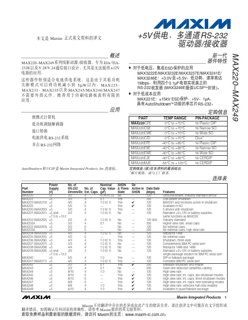
________________________________ 应用
便携式计算机 低功耗调制解调器 接口转换 电池供电 RS-232 系统 多点 RS-232 网络
_____________________________ 定购信息
PART MAX220CPE MAX220CSE MAX220CWE MAX220C/D MAX220EPE MAX220ESE MAX220EWE MAX220EJE MAX220MJE TEMP RANGE 0°C to +70°C 0°C to +70°C 0°C to +70°C 0°C to +70°C -40°C to +85°C -40°C to +85°C -40°C to +85°C -40°C to +85°C -55°C to +125°C PIN-PACKAGE 16 Plastic DIP 16 Narrow SO 16 Wide SO Dice* 16 Plastic DIP 16 Narrow SO 16 Wide SO 16 CERDIP 16 CERDIP
索取免费样品和最新版的数据资料,请访问 Maxim 的主页:。
+5V 供电、多通道 RS-232 驱动器/接收器 MAX220–MAX249
ABSOLUTE MAXIMUM RATINGS—MAX220/222/232A/233A/242/243
Supply Voltage (VCC) ...............................................-0.3V to +6V V+ (Note 1) ..................................................(VCC - 0.3V) to +14V V- (Note 1) .............................................................+0.3V to +14V Input Voltages TIN..............................................................-0.3V to (VCC - 0.3V) RIN (Except MAX220) ........................................................±30V RIN (MAX220).....................................................................±25V TOUT (Except MAX220) (Note 2) .......................................±15V TOUT (MAX220)...............................................................±13.2V Output Voltages TOUT ...................................................................................±15V ROUT .........................................................-0.3V to (VCC + 0.3V) Driver/Receiver Output Short Circuited to GND.........Continuous Continuous Power Dissipation (TA = +70°C) 16-Pin Plastic DIP (derate 10.53mW/°C above +70°C) .842mW 18-Pin Plastic DIP (derate 11.11mW/°C above +70°C)..889mW 20-Pin Plastic DIP (derate 8.00mW/°C above +70°C) ..440mW 16-Pin Narrow SO (derate 8.70mW/°C above +70°C) ...696mW 16-Pin Wide SO (derate 9.52mW/°C above +70°C)......762mW 18-Pin Wide SO (derate 9.52mW/°C above +70°C)......762mW 20-Pin Wide SO (derate 10.00mW/°C above +70°C)....800mW 20-Pin SSOP (derate 8.00mW/°C above +70°C) ..........640mW 16-Pin CERDIP (derate 10.00mW/°C above +70°C).....800mW 18-Pin CERDIP (derate 10.53mW/°C above +70°C).....842mW Operating Temperature Ranges MAX2_ _AC_ _, MAX2_ _C_ _ .............................0°C to +70°C MAX2_ _AE_ _, MAX2_ _E_ _ ..........................-40°C to +85°C MAX2_ _AM_ _, MAX2_ _M_ _ .......................-55°C to +125°C Storage Temperature Range .............................-65°C to +160°C Lead Temperature (soldering, 10s) (Note 3) ...................+300°C
MAX5437EUD+资料

♦ 50kΩ/100kΩ End-to-End Resistances
♦ Power-On Reset: Wiper Goes to Midscale
(Position 64)
Ordering Information
PART
MAX5436EUB MAX5437EUD MAX5438EUB MAX5439EUD
元器件交易网
19-2657; Rev 3; 9/04
±15V, 128-Tap, Low-Drift Digital Potentiometers
MAX5436–MAX5439
General Description
The MAX5436–MAX5439 are 128-tap high-voltage (±5V to ±15V) digital potentiometers in packages that are half the size of comparable devices in 8-pin SO. They perform the same function as mechanical potentiometers, but replace the mechanics with a simple digital interface. The digital logic is powered by a separate single +2.7V to +5.25V supply voltage (VCC). The resistor string uses its own analog supplies (VDD and VSS) that require VDD - VSS to be greater than 9V and less than 31.5V. This allows for greater flexibility in voltage ranges that can be used with these devices. Examples of analog supply ranges include not only dual voltages of ±5V to ±15V, but single-supply voltages, such as +10V, +15V, +30V, -30V, and more, as long as the ranges of VDD - VSS and VCC VSS are met. The MAX5437/MAX5439 include an on-chip, highvoltage, uncommitted amplifier, providing additional reductions in board space and cost. Other features include low 35ppm/°C end-to-end and 5ppm/°C ratiometric resistor temperature coefficients, a 3-wire SPI™/ QSPI™/MICROWIRE™-compatible serial interface, and a power-on reset to midscale. The MAX5436/MAX5438 are available in 10-pin µMAX packages. The MAX5437/MAX5439 are available in 14pin TSSOP package. Each device is guaranteed over the extended temperature range of -40°C to +85°C.
PC-6332 模入模出接口卡技术说明书

PC-6332模入模出接口卡技术说明书1.概述:PC-6332模入模出接口卡适用在具有ISA总线的PC系列微机上使用,具有很好的兼容性,CPU从目前广泛使用的64位处理器直到早期的16位处理器均可适用,操作系统可选用经典的MS-DOS,目前流行的Windows系列,高稳定性的Unix等多种操作系统以及专业数据采集分析系统LabVIEW等软件环境。
在硬件的安装上也非常简单,使用时只需将接口卡插入机内的任何一个ISA总线插槽中并用固定螺丝压紧。
其信号电缆从机箱外部直接接入。
本接口卡的模拟量输入通道为16路,允许用户采用单端输入方式或双端输入方式、用以测量单极性信号或双极性信号。
本接口卡的模出通道为1路,有电压或电流两种输出方式、共6种量程供用户选择。
其A/D转换和D/A转换均为12位。
2.主要技术参数:(标*为出厂标准状态,下同)2.1模入部分:2.1.1输入通道数:单端16路*;双端8路2.1.2输入信号范围:0V~10V*;-5V~+5V2.1.3放大器增益:硬件设置×1*;×2;×5;×10(倍)2.1.4输入阻抗:≥10MΩ2.1.5A/D转换器件:AD16742.1.6A/D转换分辨率:12位2.1.7A/D转换速度:10μS2.1.8A/D启动方式:程序启动2.1.9A/D转换非线性误差:±1LSB2.1.10A/D转换输出码制:单极性原码*/双极性偏移码2.1.11系统综合误差:≤0.1% F.S2.2模出部分:2.2.1输出通道数:1路2.2.2输出范围:电压方式:0~5V;0~10V*;-5V~+5V;电流方式:0~10mA;4~20mA(共阴方式)2.2.3输出阻抗:≤2Ω(电压方式)2.2.4D/A转换器件:AD79482.2.5D/A转换分辨率:12位2.2.6D/A转换输入码制:单极性原码*;双极性偏移码2.2.7D/A转换综合误差:电压方式:≤0.2%F.S;电流方式:≤1%F.S2.3电源功耗:+5V(±10%)≤400mA;+12V(±10%)≤100mA;-5V(±10%)≤10mA2.4使用环境:工作温度:10℃~40℃相对湿度:40%~80%存贮温度:-55℃~+85℃2.5外型尺寸:(不含档板)长×高=139.7mm×106.7mm( 5.5英寸×4.2英寸)3.工作原理:PC-6332模入模出接口卡主要由模拟多路开关电路、差分放大器电路、模数转换电路、数模转换电路及接口控制逻辑电路组成。
PC-6337 模出接口卡技术说明书

2
a. 0~10V
b. 0~5V
c. ±10V
d. ±5V
e. 1~5V
f. ±2.5V
g. 0~10mA
h. 4~20mA
图 3 D/A 输出量程及方式选择
5.5 控制端口地址与有关数据格式:
5.5.1 控制端口的操作地址与功能:各个控制端口的操作地址与功能见表 2。
表 2 端口地址与功能表
端口操作地址
一般情况下不需要调整零点,应该首先进行满度调整,尤其是在由 0~10V 方式改变为 0~5V 或 4~20mA 方式时, 更应进行此项调整。待满度调整完毕后再观察零点情况并决定是否进行调整并在必要时对满度和零点进行多次统 调,以满足使用要求。具体调整方式如下:
①基准源的调整:LM336-5.0V 基准源是为 1~5V 电压方式和 4~20mA 电流方式提供偏移基准的,出厂时已 调好。如果在使用上述两种方式时发 现偏差较大,单靠调零电位器不能正常调节时,可用电压表测量 LM-336 的 OUT 端,调节 W17 使该脚电压等于- 5.00V,或能满足使用要求即可。
空脚 电源参考地 电源参考地 电源参考地
5.3 I/O 基地址选择: I/O 基地址的选择是通过开关 K1 进行的,开关拨至 ON 处为 0,反之为 1。初始地址的选择范围一般为 0100H~
036FH 之间。用户应根据主机硬件手册给出的可用范围以及是否插入其它功能卡来决定本卡的 I/O 基地址。出 厂时本卡的基地址设为 0100H,并从基地址开始占用连续 16 个地址。现举例说明见图 2。
模拟电压值=数码(12 位) × 10(V)/4096-5
(V)
即:1 LSB 约等于 2.4414mV
其它输出量程的对应关系或可参照上面介绍的内容自行推论。
Omega PX633 潜水水位传感器说明书

P X633Submersible Level TransmitterM5720/1118Shop online at e-mail:**************For latest product manuals: Pressure transmitter is powered by an external power supply. Thepower supply circuit should comply with energy-limiting circuit by relevant standards, and pay attention to the high voltage circuits that may exist.The maximum static pressure overload has been stated on theproduct label, the process maximum pressure should not exceed the full span of sensor.When using pressure transmitter in hazardous areas, installation,use and maintenance should also comply with the operation manual and relevant requirements of national standards.Pressure transmitter should be installed by professional engineersor qualified technical personnel. The product specifications and important information provided on the label should be carefullyread before installation and wiring operations.In cases were a protective tube is unable to be used, a counterweightcan be used to stabilize a transmitter in fast flowing areas.Level transmitter probe should be higher than the bottom, at least 20cm, to avoid the blockage of impurities and sand.Submersible Level Transmitter should be suspended inside theprotective sleeve to avoid the impact on the level transmitter from fast flowing medium.Top end of protection casing should extend above the level surface, to avoid the influence on measurement accuracy from surfacedisturbances.For products with more than 50 meters cable, the wire rope and cable bundled multi-point should be used to strengthen the level transmittersupport.Clamps can be used to fix and support the entire product for direct cable connection level transmitter. Cable outlet should be of sufficient length to be directly connected to the control room, or adapter junctionbox, avoid bare connections in the field environment.It is recommended to use an independent linear direct-current power supply. Verify that the combined loop resistances (signal cable, display meter, and other equipment) are not to high, so that the voltage supplied to the pressure transmitter meets the normal operatingrequirements.Transient is effective only in the case of good grounding. Metal shell and internal grounding terminals are used to the nearest ground directly.protection module Using cable with shielded twisted-pair signal has the best effect. To avoid ground loop, shielded layer adopts single-end grounded.Standard current signal output: 12-30VDCRequires no maintenancePlease notice the following when cleaning:Use washing agent which will not damage to the instrumentsMechanical cleaning of metal diaphragm is prohibited.Protect process diaphragm from mechanical damage, eg: the mechanical damage caused by sharp objects.Do not point the nozzles to the diaphragm directly when doing internal cleaning by pressure washer.Keep dry and dust-freeStorage temperature: -30-80℃Maximum relative humidity: 95%Avoid mechanical shock and vibration Avoid solar radiationDo not store outsideDo not expose to the corrosive medium Users need to ensure the whole equipment conform to all the applicable standards.This pressure transmitter conforms to 2014/30/EU EMC standard and bears the CE markRemove all media from surfaces of the pressure transmitter. Always refer safety data sheet for proper personal protection equipment when handling dangerous medium!Please adopt proper package to avoid damage in transportation.The instrument is not restrained by WEEE instruction 2002/96/EG and laws of relevant countries.Please pass the instrument to specialized recycling companiesother than local recycling points.Connect the positive power supply (P+) to the red wire of level transmitter;Connect the negative signal module (S-) to the negative power supply (P-).Connect the positive signal module (S+) to the black wire of level transmitter;1239th March, 20151. Cable core structure:The conductor coreNumber of Core * section number of piles / Diameter Material 5×0.2mm27/0.2mm tinned copper wireInsulated wire coreMaterial Color Outer diameter PE Yellow, red, green, black, blue 1.4±0.1mmAir tubeMaterial Color Outer diameter PP Red 2.2±0.2mm2.Cabling and structureCabling direction: S (counter-clockwise)Wrapped in a layer of polyester film after stranded cableStructureFillerTinned copper braidAir tubeInsulated wireMelinexPU sheath3.Shielding144 Net tinned copper braid shielding, wrapped with a layer of polyester film after knitting.4.SheathMaterial PUColor BlackNominal thickness (mm) 0.6Outer diameter 7.3 ± 0.2mm5.FunctionWorking voltage Less than 60VDC resistance of conductor(20℃)Less than 89.6Ω/kmInsulation resistance Between the cores of cable: Over 1000MΩ/km Between the cable cores and the cable of Ground connection: Over 1000 MΩ/KMwithstand voltage between the cores of cable: 50Hz, 1kV(AC),won't be shrinking in 1minutbetween the cable cores and the cable of Ground connection: 50Hz, 1kV(AC),won't be shrinking in 1minutWorking temperature -40 to 80℃8。
MAX9652,3,4:HD视频滤波放大器
MAX9652,3,4:HD视频滤波放大器
佚名
【期刊名称】《《世界电子元器件》》
【年(卷),期】2009(000)001
【摘要】Maxim推出3通道、高清(HD)视频滤波放大器MA×9652/3/4。
器件专为高能效设计而优化,采用3.3V单电源供电。
器件每通道的静态电流仅为9.5mA,进一步降低了功耗;MAX9653/4还具有低功耗(12μA)关断模式。
该系列器件可为带有HD输出的机顶盒、AN接收机及便携式设备提供简便易用的高性价比方案。
【总页数】1页(P41)
【正文语种】中文
【中图分类】TN713
【相关文献】
1.Maxim推出汽车DirectDrive视频滤波放大器 [J],
2.MAX1150x:HDISD视频滤波器 [J],
3.MAX9532:DirectDrive视频滤波放大器 [J],
4.MAX9519:视频滤波放大器 [J],
5.Maxim推出业界首款、真正的高清视频滤波器放大器 [J],
因版权原因,仅展示原文概要,查看原文内容请购买。
常见经典【音频运放】的比较及推荐之欧阳音创编
运放名称听感和备注推荐试听封装LME49990MA×2(参考级)贴片(单运放)LME49720HA(顶级,很全面,略淡,比NA版好)1金封(外部电路有要求,NA是塑封)LM4562NA (冷峻,乐感次于49720)塑封AMP9920AS (声场宏大)贴片AMP8920VD(发烧,声场,高低频)2塑封(视频运放)OPA111BM×2(指标低于627,但音质要强)金封(单运放,正品很少,不宜作I/V 转换,OPA2111BM是双运版)OPA637BP×2(低频有力,解析很高,627的升级版)塑封(单运放,放大倍数必须大于5)OPA627BP×2(极品,华丽尊贵,胆味强于49720) 3塑封(单运放,放大倍数一般大于5)OPA1612A(人声饱满,清脆,高频细腻)贴片OPA128SM×2(泛音表现好,解析高)金封(单运放)AD797ANZ×2(柔和,人声亲切)4塑封(单运放,易自激)AD8620ARZ(浑厚,声场,人声凹陷)5贴片AD828AN(跳感,大气,延伸,中频粗糙,优于827) 6塑封(视频运放,易自激,超高SR:450V/μs,不要迷信827AQ了)AD712AQ (监听,纯净,平淡,颗粒感)7陶封OPA2228P(解析强,高频清澈)塑封OPA2107AP(均衡,甜,2111KP的升级版)塑封(不好买到,泰国的不错)OPA2111KP(安静,素质较高,女声,远差于111)8塑封(2V/μs,不宜作I/V转换,2111BM比2111KP好太多)OPA2604AP (胆味,深沉,通透,耐听)9塑封DY649FH(高频华丽,细致,女声)陶封OPA2132PA(亮丽,通透,2134的精选版)10塑封OP275G (胆味,中频圆润,少许浑)11塑封NE5532AN (经典,温暖,高频暗,5532中最好)1 2塑封(荷兰)EL2244CS(人声甜美,平淡,低频欠佳)贴片OPA2211,OPA2277,OPA2209等也是相当优秀的,不是常用运放,没有列出。
- 1、下载文档前请自行甄别文档内容的完整性,平台不提供额外的编辑、内容补充、找答案等附加服务。
- 2、"仅部分预览"的文档,不可在线预览部分如存在完整性等问题,可反馈申请退款(可完整预览的文档不适用该条件!)。
- 3、如文档侵犯您的权益,请联系客服反馈,我们会尽快为您处理(人工客服工作时间:9:00-18:30)。
General DescriptionThe MAX6332/MAX6333/MAX6334 microprocessor (µP)supervisory circuits monitor the power supplies in 1.8V to 3.3V µP and digital systems. They increase circuit reliability and reduce cost by eliminating external com-ponents and adjustments.These devices perform a single function: they assert a reset signal whenever the V CC supply voltage declines below a preset threshold, keeping it asserted for a pre-set timeout period after V CC has risen above the reset threshold. The only difference among the three devices is their output. The MAX6333 (push/pull) and MAX6334(open-drain) have an active-low RESET output, while the MAX6332 (push/pull) has an active-high RESET out-put. The MAX6332/MAX6333 are guaranteed to be in the correct state for V CC down to 0.7V. The MAX6334 is guaranteed to be in the correct state for V CC down to 1.0V.The reset comparator in these ICs is designed to ignore fast transients on V CC . Reset thresholds are factory-trimmable between 1.6V and 2.5V, in approximately 100mV increments. There are 15 standard versions available (2,500 piece minimum-order quantity); con-tact the factory for availability of nonstandard versions (10,000 piece minimum-order quantity). For space-criti-cal applications, the MAX6332/MAX6333/MAX6334come packaged in a 3-pin SOT23.ApplicationsPentium II™ Computers Computers ControllersIntelligent InstrumentsCritical µP/µC Power Monitoring Portable/Battery-Powered Equipment AutomotiveFeatures♦Ultra-Low 0.7V Operating Supply Voltage♦Low 3.3µA Supply Current♦Precision Monitoring of 1.8V and 2.5V Power-Supply Voltages ♦Reset Thresholds Available from 1.6V to 2.5V,in Approximately 100mV Increments ♦Fully Specified over Temperature♦Three Power-On Reset Pulse Widths Available (1ms min, 20ms min, 100ms min)♦Low Cost♦Three Available Output Structures: Push/Pull RESET , Push/Pull RESET, Open-Drain RESET ♦Guaranteed RESET/RESET Valid to V CC = 0.7V (MAX6332/MAX6333)♦Power-Supply Transient Immunity ♦No External Components ♦3-Pin SOT23 Package♦Pin Compatible with MAX809/MAX810 and MAX6326/MAX6327/MAX6328MAX6332/MAX6333/MAX63343-Pin, Ultra-Low-Voltage, Low-PowerµP Reset Circuits________________________________________________________________Maxim Integrated Products119-1411; Rev 2; 12/05Ordering Information* These devices are available in factory-set V CC reset thresh-olds from 1.6V to 2.5V, in approximately 0.1V increments.Choose the desired reset threshold suffix from Table 1 and insert it in the blanks following “UR” in the part number.Factory-programmed reset timeout periods are also available.Insert the number corresponding to the desired nominal reset timeout period (1 = 1ms min, 2 = 20ms min, 3 = 100ms min) in the blank following “D” in the part number. There are 15 stan-dard versions with a required order increment of 2500 pieces.Sample stock is generally held on the standard versions only (see Selector Guide). Contact the factory for availability of non-standard versions (required order increment is 10,000 pieces).All devices available in tape-and-reel only.Devices are available in both leaded and lead-free packaging.Specify lead-free by replacing “-T” with “+T” when ordering.Typical Operating Circuit and Pin Configuration appear at end of data sheet.Selector Guide appears at end of data sheet.Pentium II is a trademark of Intel Corp.For pricing, delivery, and ordering information,please contact Maxim/Dallas Direct!at 1-888-629-4642, or visit Maxim’s website at .M A X 6332/M A X 6333/M A X 63343-Pin, Ultra-Low-Voltage, Low-Power µP Reset Circuits 2_______________________________________________________________________________________ABSOLUTE MAXIMUM RATINGSELECTRICAL CHARACTERISTICS(V CC = full range, T A = -40°C to +125°C, unless otherwise noted. Typical values are at T A = +25°C and V CC = 3V, reset not assert-Stresses beyond those listed under “Absolute Maximum Ratings” may cause permanent damage to the device. These are stress ratings only, and functional operation of the device at these or any other conditions beyond those indicated in the operational sections of the specifications is not implied. Exposure to absolute maximum rating conditions for extended periods may affect device reliability.Terminal Voltage (with respect to GND)V CC ......................................................................-0.3V to +6V Push/Pull RESET, RESET .......................-0.3V to (V CC + 0.3V)Open-Drain RESET ..............................................-0.3V to +6V Input Current (V CC ).............................................................20mA Output Current (RESET, RESET ).........................................20mAContinuous Power Dissipation (T A = +70°C)SOT23-3 (derate 4mW/°C above +70°C)....................320mW Operating Temperature Range .........................-40°C to +125°C Storage Temperature Range.............................-65°C to +160°C Lead Temperature (soldering, 10s).................................+300°C3-Pin, Ultra-Low-Voltage, Low-PowerµP Reset Circuits_______________________________________________________________________________________32.02.62.23.03.63.83.43.24.0-602.4-40-202.820406080100SUPPLY CURRENT vs. TEMPERATURETEMPERATURE (°C)I C C (µA )0.9500.9900.9701.0001.0301.0401.0201.0101.050-60-400.980-2000.96020406080100NORMALIZED RESET TIMEOUT PERIODvs. TEMPERATURETEMPERATURE (°C)N O R M A L I Z E D R E S E T T I M E O U T P E R I O D1020-20403070605080-600-4020406080100V CCFALLING PROPAGATION DELAYvs. TEMPERATURETEMPERATURE (°C)P R O P A G A T I O N D E L A Y (µs )10010001002004003005006000.1110MAXIMUM TRANSIENT DURATION vs. RESET COMPARATOR OVERDRIVERESET COMPARATOR OVERDRIVE (mV)M A X I M U M T R A N S I E N T D U R A T I O N (µs )402080601001201401600.5 1.0 1.250.75 1.5 1.75 2.0 2.25 2.5OUTPUT VOLTAGE HIGH vs. SUPPLY VOLTAGEV CC (V)O U T P U T V O L T A G E H I G H (V C C - V O H ) (m V )20103060705040800.5 1.00 1.50 2.00 2.50 3.00OUTPUT VOLTAGE LOW vs. SUPPLY VOLTAGEV CC (V)O U T P U T V O L T A G E L O W (m V )Typical Operating Characteristics(Reset not asserted, T A = +25°C, unless otherwise noted.)MAX6332/MAX6333/MAX6334Pin DescriptionM A X 6332/M A X 6333/M A X 63343-Pin, Ultra-Low-Voltage, Low-Power µP Reset Circuits 4_____________________________________________________________________________________________________Applications InformationInterfacing to µPs with BidirectionalReset PinsSince the RESET output on the MAX6334 is open-drain,this device interfaces easily with µPs that have bidirec-tional reset pins, such as the Motorola 68HC11.Connecting the µP supervisor’s RESET output directly to the microcontroller’s (µC’s) RESET pin with a single pull-up resistor allows either device to assert reset (Figure 1).Negative-Going V CC TransientsIn addition to issuing a reset to the µP during power-up,power-down, and brownout conditions, these devices are relatively immune to short-duration, negative-going V CC transients (glitches). The Typical Operating Characteristics show the Maximum Transient Duration vs. Reset Comparator Overdrive graph. The graph shows the maxi-mum pulse width that a negative-going V CC transient may typically have without issuing a reset signal. As the ampli-tude of the transient increases, the maximum allowable pulse width decreases.Ensuring a Valid Reset OutputDown to V CC = 0When V CC falls below 1V and approaches the minimum operating voltage of 0.7V, push/pull-structured reset sinking (or sourcing) capabilities decrease drastically.High-impedance CMOS-logic inputs connected to the RESET pin can drift to indeterminate voltages. This does not present a problem in most cases, since most µPs and circuitry do not operate at V CC below 1V. For the MAX6333, where RESET must be valid down to 0,adding a pull-down resistor between RESET and GND removes stray leakage currents, holding RESET low (Figure 2a). The pull-down resistor value is not critical;100k Ωis large enough not to load RESET and small enough to pull it low. For the MAX6332, where RESET must be valid to V CC = 0, a 100k Ωpull-up resistor between RESET and V CC will hold RESET high when V CC falls below 0.7V (Figure 2b).Since the MAX6334 has an open-drain, active-low out-put, it typically uses a pull-up resistor. With this device,RESET will most likely not maintain an active condition,but will drift to a non-active level due to the pull-up resistor and the reduced sinking capability of the open-drain device. Therefore, this device is not recommend-ed for applications where the RESET pin is required to be valid down to V CC = 0.* Factory-trimmed reset thresholds are available in approximately 100mV increments, with a ±1.8% room-temperature variance.Table 1. Factory-Trimmed Reset Thresholds*Figure 1. Interfacing to µPs with Bidirectional Reset PinsFigure 2. Ensuring Reset Valid Down to V CC = 03-Pin, Ultra-Low-Voltage, Low-PowerµP Reset Circuits_______________________________________________________________________________________5MAX6332/MAX6333/MAX6334Pin ConfigurationSelector Guide (Standard Versions *)Typical Operating Circuit* Sample stock is generally held on all standard versions.M A X 6332/M A X 6333/M A X 63343-Pin, Ultra-Low-Voltage, Low-Power µP Reset Circuits Maxim cannot assume responsibility for use of any circuitry other than circuitry entirely embodied in a Maxim product. No circuit patent licenses are implied. Maxim reserves the right to change the circuitry and specifications without notice at any time.6_____________________Maxim Integrated Products, 120 San Gabriel Drive, Sunnyvale, CA 94086 408-737-7600©2005 Maxim Integrated ProductsPrinted USAis a registered trademark of Maxim Integrated Products, Inc.TRANSISTOR COUNT:505Chip InformationPackage Information(The package drawing(s) in this data sheet may not reflect the most current specifications. For the latest package outline information,go to /packages .)。
