MAX6359TVUT中文资料
MAX832中文资料
NUAL KIT MA ATION U EET L H A S V A E T WS DA FOLLO
___________________________Features
o Input Range: Up to 30V o 1A On-Chip Power Switch o Adjustable Output (MAX830) Fixed Outputs: 5V (MAX831) 3.3V (MAX832) 3V (MAX833) o 100kHz Switching Frequency o Excellent Dynamic Characteristics o Few External Components o 8mA Quiescent Current o 16-Pin SO Package o Evaluation Kit Available
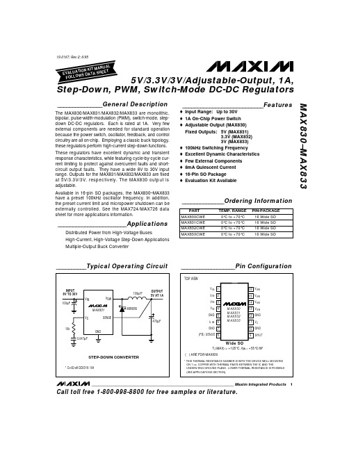
__________Typical Operating Circuit
__________________Pin Configuration
TOP VIEW
INPUT 8V TO 30V 100µF VIN VSW
100µH*
OUTPUT 5V AT 1A
V IN 1 V IN 2 V IN 3
16 V SW 15 V SW 14 V SW
_______________________Applications
Distributed Power from High-Voltage Buses High-Current, High-Voltage Step-Down Applications Multiple-Output Buck Converter
MAX831
VC 10k 0.047µF SENSE
MAX2990中文资料
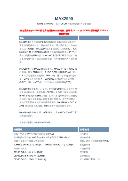
传感器控制和数据采集 电力线传输语音设备
Key Specifications: Powerline Networking Devices
Part Features
Number
Security Features
Smalles
t
Budgetary
Availabl Oper. Interf EV Package e Pckg. Temp.
MAX2990
10kHz 至 490kHz、基于 OFDM 的电力线通信调制解调器
业内首款基于 OFDM 的电力线通信调制解调器,能够在 10kHz 至 490kHz 频带提供 100kbps 的数据传输
概述
MAX2990 电力线通信(PLC)基带调制解调器可通过交流或直 流电力线提供高性价比且可靠的半双工异步数据通信,传输速 率高达 100kbps。MAX2990 是高集成度片上系统(SoC),利用 Maxim 的 16 位 RISC MAXQ 微控制器核构建物理层(PHY)和 媒体访问控制(MAC)层。MAX2990 采用 OFDM 调制技术,可 在电力网络中进行稳定的数据传输,同时为网络的所有器件供 电。
Yes LQFP/64
Compliant to
Serial
Managemen
FCC,
UART
t
CENELEC,
148.8
-40 to $8.50 @1k
+85
ARIB
Data Rate Up
to 100Kbps
OFDM-Based
PHY
查看所有 Powerline Networking Devices (5)
Pricing Notes:
This pricing is BUDGETARY, for comparing similar parts. Prices are in U.S. dollars and subject to change. Quantity pricing may vary substantially and international prices may differ due to local duties, taxes, fees, and exchange rates. For volume-specific prices and delivery, please see the price and availability page or contact an authorized distributor.
MAX4636中文资料

元器件交易网
Fast, Low-Voltage, Dual 4Ω SPDT CMOS Analog Switches MAX4635/MAX4636
ABSOLUTE MAXIMUM RATINGS
(Voltages Referenced to GND) V+, IN_ .....................................................................-0.3V to +6V COM_, NC_, NO_ (Note 1) .......................... -0.3V to (V+ + 0.3V) Continuous Current into Any Terminal .............................±30mA Peak Current into COM_, NC_, NO_ (pulsed at 1ms, 10% duty cycle).................................±100mA Continuous Power Dissipation (TA = +70°C) 10-Pin µMAX (derate 4.7mW/°C above +70°C) ............330mW 10-Pin Thin QFN (derate 24.4mW/°C above +70°C) ..1951mW Operating Temperature Range .......................... -40°C to +85°C Storage Temperature Range ........................... -65°C to +150°C Lead Temperature (soldering, 10s) ............................... +300°C
MAX6349VHUT中文资料
________________________Applications
Hand-Held Instruments
Electronic Planners
Palm Top Computers
PCMCIA Cards
USB Devices
Cellular Telephones
Cordless Telephones
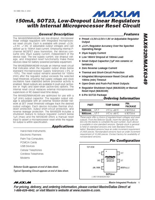
The MAX6329/MAX6349 are optimized for use with a 1µF (min) output capacitor. The regulator output voltage is adjustable with an external resistor-divider network at SET (reset threshold voltages track the desired output voltage). Each device includes thermal shutdown protection, output short-circuit protection, and reverse leakage protection. The MAX6329 includes a shutdown feature to reduce regulator current below 1µA (max) and the MAX6349 offers a manual reset input to assert a microprocessor reset while the regulator output is within specification.
芯片MAX691中文资料

微处理器监控电路MAX691介绍2008年11月07日星期五 22:20max691介绍_微处理器监控电路作者:汪龙景整理:nemoiumMAX691是美国MAXIM公司生产的微处理器监控电路。
由于技术先进,功能完整,精度较高,该电路在自动控制、自动测量及便携产品等领域得到广泛应用。
在法国 THOMCAST公司生和的E—UHF—10003全固态电视发射机中,该芯片应用有六处之多。
现将该集成电路的结构、原理及应用简单介绍如下:一、引脚排列及说明图1所示为MAX691的引脚排列图,分别说明如下:1、VBAn,臼备用电池输入端,连接到外部电池或电容器的充电电路,不用时接地。
2、Vovr一电源电压输出端,不使用备用电池时,可接到Vuo3、Vcc一电源电压输入端。
正常时应为 +5V。
4、GND--~地端5、BATT 0N—电池接通标志端。
当 VouT转接到VBATY时,变为高电平。
6.LOWLINE~电源电压降低标志端。
当 Vcc低于复位门限电压时,LOWLINE 变为低电平。
7、OSC IN—外部振荡器输入端。
8、OSC SEI广振荡器选择端。
9、Pp卜电源故障输入端。
不使用时接地或接Votrro10、PFO一电源故障输出端。
当PFI小于 1.25V时PFO变为低电平。
11、WD卜看门狗输入端。
不使用看门狗功能时悬空。
12、CEOUT—芯片使用输出端13、CEIN—芯片使用输入端。
不使用时接地或接Votrro14、WOD—‘看门狗输出端。
15、RESm,隅复位脉冲输出端,低电平有效。
16、RKSm,畸高电平有效的复位脉冲输出端,该端为漏极开路输出。
一、内部结构及工作原理图2所示为MAX691的内部结构方框图。
由图2知,该集成电路主要由以下几部分组成:1、电源监测及切换电路图2中,两个电压比较器C1、C2,电源切换开关及4.65V的基准电压源等构成电源监测及切换部分。
4。
65V的基准电压源产生复位门限电平,Ve与它在C:中进行比较。
MAXIM MAX3570 MAX3571 MAX3573 说明书

_________________________________概述MAX3570/MAX3571/MAX3573低成本、宽带、两次变频调谐器芯片设计用于数字电视接收机。
每款芯片集成了所有必需的射频功能模块,其中包括一个集成的高中频滤波器、全集成VCO、中频VGA。
工作频率范围从50MHz 至878MHz,同时提供超过60dB的RF及IF可控增益范围。
MAX3570/MAX3571具有以44MHz为中心的中频频率,而MAX3573具有以36MHz为中心的中频输出。
这三款芯片都包括了可变增益射频前端,噪声系数仅为8dB。
双频合成器产生两个本振(LO)频率,提供优异的相位噪声性能,在10kHz频偏时相位噪声为-86dBc/Hz。
集成的高中频(HI-IF)滤波器有55dBc (典型值)的镜像抑制。
仅需要一个中频SAW滤波器、无源环路滤波器和晶体振荡器即可构建完整的单芯片调谐器。
MAX3570芯片编程和配置由3线串行接口完成,而MAX3571/MAX3573芯片编程和配置由2线串行接口完成。
MAX3570/MAX3571/MAX3573采用48引脚QFN-EP封装,可工作于商业温度范围(0°C 至+70°C)。
_________________________________应用DVB-C数字电视接收机ATSC数字电视接收机有线电视调制解调器DOCSIS/EURO DOCSIS调制解调器ITU J.83数字机顶盒___________________________________特性♦全集成HI-IF滤波器♦全集成VCO,无需外部元器件和走线。
♦8dB低噪声系数♦高线性—大于54dBc, CSO, CTB, X-MOD。
♦业界最小的封装♦优异的相位噪声,可用于256-QAM、8-VSB和COFDM。
MAX3570/MAX3571/MAX3573高中频(HI-IF)单片宽带调谐器________________________________________________________________Maxim Integrated Products1_____________________引脚排列和功能框图______________________________定购信息*EP = 裸露焊盘。
MAX4590EAE-T中文资料
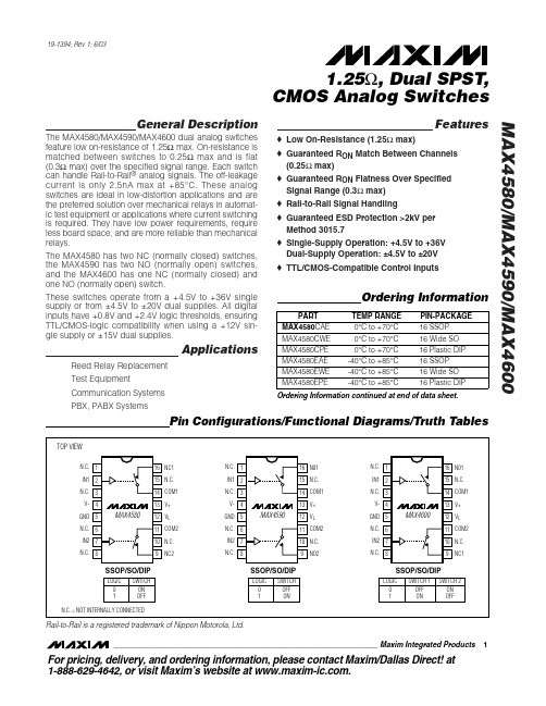
General DescriptionThe MAX4580/MAX4590/MAX4600 dual analog switches feature low on-resistance of 1.25Ωmax. On-resistance is matched between switches to 0.25Ωmax and is flat (0.3Ωmax) over the specified signal range. Each switch can handle Rail-to-Rail ®analog signals. The off-leakage current is only 2.5nA max at +85°C. These analog switches are ideal in low-distortion applications and are the preferred solution over mechanical relays in automat-ic test equipment or applications where current switching is required. They have low power requirements, require less board space, and are more reliable than mechanical relays.The MAX4580 has two NC (normally closed) switches,the MAX4590 has two NO (normally open) switches,and the MAX4600 has one NC (normally closed) and one NO (normally open) switch.These switches operate from a +4.5V to +36V single supply or from ±4.5V to ±20V dual supplies. All digital inputs have +0.8V and +2.4V logic thresholds, ensuring TTL/CMOS-logic compatibility when using a +12V sin-gle supply or ±15V dual supplies.ApplicationsReed Relay Replacement Test EquipmentCommunication Systems PBX, PABX SystemsFeatureso Low On-Resistance (1.25Ωmax)o Guaranteed R ON Match Between Channels (0.25Ωmax)o Guaranteed R ON Flatness Over Specified Signal Range (0.3Ωmax)o Rail-to-Rail Signal Handlingo Guaranteed ESD Protection >2kV per Method 3015.7o Single-Supply Operation: +4.5V to +36V Dual-Supply Operation: ±4.5V to ±20V o TTL/CMOS-Compatible Control InputsMAX4580/MAX4590/MAX46001.25Ω, Dual SPST,CMOS Analog Switches________________________________________________________________Maxim Integrated Products119-1394; Rev 1; 6/03Ordering Information continued at end of data sheet.Rail-to-Rail is a registered trademark of Nippon Motorola, Ltd.Pin Configurations/Functional Diagrams/Truth TablesOrdering InformationFor pricing, delivery, and ordering information,please contact Maxim/Dallas Direct!at 1-888-629-4642, or visit Maxim’s website at .M A X 4580/M A X 4590/M A X 46001.25Ω, Dual SPST,CMOS Analog Switches 2_______________________________________________________________________________________ABSOLUTE MAXIMUM RATINGSStresses beyond those listed under “Absolute Maximum Ratings” may cause permanent damage to the device. These are stress ratings only, and functional operation of the device at these or any other conditions beyond those indicated in the operational sections of the specifications is not implied. Exposure to absolute maximum rating conditions for extended periods may affect device reliability.V+ to GND..............................................................-0.3V to +44V V- to GND...............................................................+0.3V to -44V V+ to V-...................................................................-0.3V to +44V V L to GND....................................................-0.3V to (V+ + 0.3V)All Other Pins to GND (Note 1) ...........(V- - 0.3V) to (V+ + 0.3V)Continuous Current (COM_, NO_, NC_) .......................±200mA Peak Current (COM_, NO_, NC_)(pulsed at 1ms, 10% duty cycle) ..............................±300mAContinuous Power Dissipation (T A = +70°C)16 SSOP (derate 7.1mW/°C above +70°C).................571mW 16 Wide SO (derate 9.52mW/°C above +70°C) ..........762mW 16 Plastic DIP (derate 10.53mW/°C above +70°C).....842mW Operating Temperature RangesMAX4_ _0C_E ....................................................0°C to +70°C MAX4_ _0E_E ..................................................-40°C to +85°C Storage Temperature Range ...........................-65°C to +160°C Lead Temperature (soldering, 10sec) ............................+300°CELECTRICAL CHARACTERISTICS–Dual Supplies(V+ = +15V, V- = -15V, V L = +5V, V IN_H = +2.4V, V IN_L = +0.8V, T A = T MIN to T MAX , unless otherwise noted. Typical values are at T A = +25°C.)Note 1:Signals on NC_, NO_, COM_, or IN_ exceeding V+ or V- are clamped by internal diodes. Limit forward diode current tomaximum current rating.ELECTRICAL CHARACTERISTICS–Dual Supplies (continued)MAX4580/MAX4590/MAX46001.25Ω, Dual SPST,CMOS Analog Switches (V+ = +15V, V- = -15V, V L= +5V, V IN_H= +2.4V, V IN_L= +0.8V, T A = T MIN to T MAX, unless otherwise noted. Typical values are atT A= +25°C.)_______________________________________________________________________________________3M A X 4580/M A X 4590/M A X 46001.25Ω, Dual SPST,CMOS Analog Switches 4_______________________________________________________________________________________ELECTRICAL CHARACTERISTICS–Single Supply(V+ = +12V, V- = 0, V L = +5V, V INH = 2.4V, V INL = 0.8V, T A = T MIN to T MAX , unless otherwise noted. Typical values are at T = +25°C.)MAX4580/MAX4590/MAX46001.25Ω, Dual SPST,CMOS Analog Switches_______________________________________________________________________________________5ELECTRICAL CHARACTERISTICS—Single Supply (continued)(V+ = +12V, V- = 0, V L = +5V, V IN_H = 2.4V, V IN_L = 0.8V, T A = T MIN to T MAX , unless otherwise noted. Typical values are at T A = +25°C.)Note 2:The algebraic convention, where the most negative value is a minimum and the most positive value a maximum, is used inthis data sheet.Note 3:Guaranteed by design.Note 4:∆R ON = R ON(MAX)- R ON(MIN).Note 5:Flatness is defined as the difference between the maximum and minimum value of on-resistance as measured over thespecified analog signal range.Note 6:Leakage parameters are 100% tested at maximum-rated hot temperature and guaranteed by correlation at +25°C.Note 7:Off-isolation = 20 log 10[V COM / (V NC or V NO )], V COM = output, V NC or V NO = input to off switch.Note 8:Between any two switches.Note 9:Leakage testing at single supply is guaranteed by testing with dual supplies.0.51.01.52.02.5-20-12-8-16-448121620ON-RESISTANCE vs. V COM(DUAL SUPPLIES)V COM (V)R O N (Ω)ON-RESISTANCE vs. V COMAND TEMPERATURE (DUAL SUPPLIES)V COM (V)R O N (Ω)129-12-9-63-360.50.60.70.80.91.01.11.20.4-1515ON-RESISTANCE vs. V COM(SINGLE SUPPLY)V COM (V)R O N (Ω)2220181614121086421234524Typical Operating Characteristics(Circuit of Figure 1, T A = +25°C, unless otherwise noted.)Typical Operating Characteristics (continued)(Circuit of Figure 1, T A = +25°C, unless otherwise noted.)M A X 4580/M A X 4590/M A X 46001.25Ω, Dual SPST,CMOS Analog Switches 6_______________________________________________________________________________________ON-RESISTANCE vs. V COMAND TEMPERATURE (SINGLE SUPPLY)V COM (V)R O N (Ω)11108923456710.250.500.751.001.251.501.752.002.2500120.0010.010.11100101000-4020-20406080100POWER-SUPPLY CURRENTvs. TEMPERATURETEMPERATURE (°C)I +, I - (n A )10,0000.0010.01110-4020-20406080100ON/OFF-LEAKAGE vs. TEMPERATURETEMPERATURE (°C)L E A K A G E (n A )-500-3000200400-400-100100300500-15-50-10515CHARGE INJECTIONvs. V COMV COM (V)Q (p C )10-2000-1000.011100.1100-80FREQUENCY (MHz)L O S S (d B )P H A S E (d e g r e e s )-60-40-20-90-70-50-30-10+180-720-540-360-1800-630-450-270-90+9050100150250300-4010-15356085TURN-ON/TURN-OFF TIME vs. TEMPERATURETEMPERATURE (°C)t O N , t O F F (n s )MAX4580/MAX4590/MAX46001.25Ω, Dual SPST,CMOS Analog Switches_______________________________________________________________________________________7801202001602402801012111314151617181920TURN-ON/TURN-OFF TIME vs. SUPPLY VOLTAGEV+, V- (V)t O N , t O F F (n s )Typical Operating Characteristics (continued)(Circuit of Figure 1, T A = +25°C, unless otherwise noted.)TURN-ON/TURN-OFF TIME vs. V COMV COM (V)t O N , t O F F (n s )8642-2-4-6-8120140160180200220100-1010Pin DescriptionM A X 4580/M A X 4590/M A X 46001.25Ω, Dual SPST,CMOS Analog Switches8__________________________________________________________________________________________________Applications InformationOvervoltage ProtectionProper power-supply sequencing is recommended for all CMOS devices. Do not exceed the absolute maxi-mum ratings, because stresses beyond the listed rat-ings can cause permanent damage to the devices.Always sequence V+ on first, then V-, followed by the logic inputs, NO, or COM. If power-supply sequencing is not possible, add two small signal diodes (D1, D2) in series with supply pins for overvoltage protection (Figure 1). Adding diodes reduces the analog signal range to one diode drop below V+ and one diode drop above V-, but does not affect the devices’ low switch resistance and low leakage characteristics. Device operation is unchanged, and the difference between V+and V- should not exceed 44V. These protection diodes are not recommended when using a single supply.Figure 1. Overvoltage Protection Using External Blocking DiodesFigure 2. Switching-Time Test CircuitMAX4580/MAX4590/MAX46001.25Ω, Dual SPST,CMOS Analog Switches_______________________________________________________________________________________9Figure 4. Off-Isolation Test Circuit Figure 5. Crosstalk Test CircuitM A X 4580/M A X 4590/M A X 46001.25Ω, Dual SPST,CMOS Analog Switches 10______________________________________________________________________________________Ordering Information (continued)___________________Chip InformationTRANSISTOR COUNT: 100Figure 6. Switch Off-Capacitance Test CircuitFigure 7. Switch On-Capacitance Test CircuitPackage InformationMAX4580/MAX4590/MAX46001.25Ω, Dual SPST,CMOS Analog Switches (The package drawing(s) in this data sheet may not reflect the most current specifications. For the latest package outline informationgo to /packages.) Array______________________________________________________________________________________11M A X 4580/M A X 4590/M A X 46001.25Ω, Dual SPST,CMOS Analog Switches S O I C W .E P SPackage Information (continued)(The package drawing(s) in this data sheet may not reflect the most current specifications. For the latest package outline information go to /packages .)Ma xim ca nnot a ssume responsibility for use of a ny circuitry other tha n circuitry entirely embodied in a Ma xim product. No circuit pa tent licenses a re implied. Maxim reserves the right to change the circuitry and specifications without notice at any time.12____________________Maxim Integrated Products, 120 San Gabriel Drive, Sunnyvale, CA 94086 408-737-7600©2003 Maxim Integrated ProductsPrinted USAis a registered trademark of Maxim Integrated Products.。
MAX4395ESD+中文资料
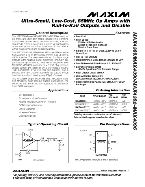
General DescriptionThe MAX4389/MAX4390/MAX4392–MAX4396 family of op amps are unity-gain stable devices that combine high-speed performance, rail-to-rail outputs, and dis-able mode. These devices are targeted for applications where an input or an output is exposed to the outside world, such as video and communications.The MAX4389/MAX4390/MAX4392–MAX4396 operate from a single 4.5V to 11V supply or from dual ±2.25V to ±5.5V supplies. The common-mode input voltage range extends to the negative power-supply rail (ground in sin-gle-supply applications). The MAX4389/MAX4390/MAX4392–MAX4396 consume only 5.5mA of quinescent supply current per amplifier while achieving a 85MHz -3dB bandwidth, 27MHz 0.1dB gain flatness, and a 500V/µs slew rate. Disable mode sets the outputs to high impedance while consuming only 450µA of current.The MAX4389 single, MAX4393 dual, MAX4394 triple,and MAX4396 quad include disable capabilities. The MAX4389 and MAX4390 are available in ultra-small,6-pin SC70 packages.ApplicationsSet-Top BoxesSurveillance Video SystemsAnalog-to-Digital Converter Interface CCD Imaging Systems Digital Cameras Video-on-Demand Video Line DriverFeatures♦Low Cost ♦High Speed85MHz -3dB Bandwidth 27MHz 0.1dB Gain Flatness 500V/µs Slew Rate♦Single 4.5V to 11V or Dual ±2.25V to ±5.5V Operation♦Rail-to-Rail Outputs♦Input Common-Mode Range Extends to V EE ♦Low Differential Gain/Phase: 0.015%/0.015°♦Low Distortion at 5MHz-59dBc Spurious-Free Dynamic Range ♦High Output Drive: ±50mA ♦450µA Disable Capability(MAX4389/MAX4393/MAX4394/MAX4396)♦Space-Saving SC70, SOT23, µMAX, or TSSOP PackagesMAX4389/MAX4390/MAX4392–MAX4396Ultra-Small, Low-Cost, 85MHz Op Amps withRail-to-Rail Outputs and Disable________________________________________________________________Maxim Integrated Products 1Pin Configurations19-2322; Rev 3; 8/04For pricing, delivery, and ordering information,please contact Maxim/Dallas Direct!at 1-888-629-4642, or visit Maxim’s website at .Ordering InformationTypical Operating CircuitOrdering Information continued at end of data sheet.Selector Guide appears at end of data sheet.M A X 4389/M A X 4390/M A X 4392–M A X 4396Ultra-Small, Low-Cost, 85MHz Op Amps with Rail-to-Rail Outputs and DisableABSOLUTE MAXIMUM RATINGSStresses beyond those listed under “Absolute Maximum Ratings” may cause permanent damage to the device. These are stress ratings only, and functional operation of the device at these or any other conditions beyond those indicated in the operational sections of the specifications is not implied. Exposure to absolute maximum rating conditions for extended periods may affect device reliability.Supply Voltage (V CC to V EE )..................................-0.3V to +12V IN_+, IN_-, OUT_, DISABLE .............(V EE - 0.3V) to (V CC + 0.3V)Differential Input Voltage ....................................................±2.5V Current into Input Pins......................................................±20mA Output Short-Circuit Duration toV CC or V EE (Note 1)................................................Continuous Continuous Power Dissipation (T A = +70°C)5-Pin SOT23 (derate 7.1mW/°C above +70°C)............571mW 6-Pin SOT23 (derate 8.7mW/°C above +70°C)............696mW 6-Pin SC70 (derate 3.1mW/°C above +70°C)..............245mW 8-Pin SO (derate 5.88mW/°C above +70°C)................471mW 8-Pin µMAX (derate 4.5mW/°C above +70°C).............362mW 10-Pin µMAX (derate 5.6mW/°C above +70°C)...........444mW 14-Pin SO (derate 8.33mW/°C above +70°C)..............667mW 14-Pin TSSOP (derate 10mW/°C above +70°C)..........727mW 20-Pin TSSOP (derate 10.9mW/°C above +70°C).......879mW Operating Temperature Range ...........................-40°C to +85°C Junction Temperature......................................................+150°C Storage Temperature Range.............................-65°C to +150°C Lead Temperature (soldering, 10s).................................+300°CDC ELECTRICAL CHARACTERISTICS—Single SupplyNote 1:Continuous power dissipation must also be observed.MAX4389/MAX4390/MAX4392–MAX4396Ultra-Small, Low-Cost, 85MHz Op Amps withRail-to-Rail Outputs and Disable_______________________________________________________________________________________3DC ELECTRICAL CHARACTERISTICS—Dual SupplyDC ELECTRICAL CHARACTERISTICS—Single Supply (continued)(V CC = 5V, V EE = 0V, V CM = V CC /2, V OUT = V CC /2, R L = ∞to V CC /2, DISABLE_= V CC (MAX4389/MAX4393/MAX4394/MAX4396),T A = T MIN to T MAX , unless otherwise noted. Typical values are at T A = +25°C.) (Note 2)M A X 4389/M A X 4390/M A X 4392–M A X 4396Ultra-Small, Low-Cost, 85MHz Op Amps with Rail-to-Rail Outputs and Disable 4_______________________________________________________________________________________AC ELECTRICAL CHARACTERISTICS—Single SupplyDC ELECTRICAL CHARACTERISTICS—Dual Supply (continued)(V CC = 5V, V EE = -5V, V CM = 0V, V OUT = 0V, R L = ∞to 0, DISABLE_= V CC (MAX4389/MAX4393/MAX4394/MAX4396),T A = T MIN to T MAX , unless otherwise noted. Typical values are at T A = +25°C.) (Note 2)MAX4389/MAX4390/MAX4392–MAX4396Ultra-Small, Low-Cost, 85MHz Op Amps withRail-to-Rail Outputs and Disable_______________________________________________________________________________________5Note 2:All devices are 100% production tested at T A = +25°C. Specifications over temperature limits are guaranteed by design.AC ELECTRICAL CHARACTERISTICS—Dual SupplyAC ELECTRICAL CHARACTERISTICS—Single Supply (continued)GAIN AND PHASE vs. FREQUENCYFREQUENCY (Hz)G A I N (d B )100M1M10M10k100k-100-80-60-40-20020406080-120P H A S E (D E G R E E S )-225-180-135-90-4504590135180-2701k1GSMALL-SIGNAL GAIN vs. FREQUENCYFREQUENCY (Hz)G A I N (d B )100M 10M 1M -5-4-3-2-101234-6100k 1GLARGE-SIGNAL GAIN vs. FREQUENCYFREQUENCY (Hz)G A I N (d B )100M 10M 1M -5-4-3-2-101234-6100k 1GSMALL-SIGNAL GAIN FLATNESS vs. FREQUENCYFREQUENCY (Hz)G A I N (d B )100M 10M 1M -0.5-0.4-0.3-0.2-0.100.10.20.30.4-0.6100k 1GDISTORTION vs. FREQUENCYFREQUENCY (Hz)D I S T O R T I O N (d B c )10M 1M -80-90-70-60-50-40-30-20-100-100100k 100MLARGE-SIGNAL GAIN FLATNESS vs. FREQUENCYFREQUENCY (Hz)G A I N (d B )100M10M 1M-0.5-0.4-0.3-0.2-0.100.10.20.30.4-0.6100k1GOUTPUT IMPEDANCE vs. FREQUENCYM A X 4389 t o c 06FREQUENCY (Hz)O U T P U T I M P E D A N C E (Ω)100M 10M 1M 0.11101000.01100k1GDISTORTION vs. FREQUENCYFREQUENCY (Hz)D I S T O R T I O N (d B c )10M 1M -80-90-70-60-50-40-30-20-100-100100k 100MDISTORTION vs. FREQUENCYFREQUENCY (Hz)D I S T O R T I O N (d B c )10M 1M -80-90-70-60-50-40-30-20-100-100100k 100MTypical Operating Characteristics(V CC = 5V, V EE = -5V, V CM = 0V, A VCL = 1V/V, R L = 100Ωto GND, GND = 0, T A = +25°C, unless otherwise noted.)M A X 4389/M A X 4390/M A X 4392–M A X 4396Ultra-Small, Low-Cost, 85MHz Op Amps with Rail-to-Rail Outputs and Disable 6_______________________________________________________________________________________DISTORTION vs. RESISTIVE LOADVOLTAGE SWING (V P-P )D I S T O R T I O N (d B c )8001000200400600-80-70-60-50-40-30-20-10-9001200-100DISTORTION vs. VOLTAGE SWINGVOLTAGE SWING (V P-P )D I S T O R T I O N (d B c )1.51.0-90-70-80-60-50-40-30-20-10-1000.52.0DIFFERENTIAL GAIN AND PHASEIRED I F F G A I N (%)23451D I F F P H A SE (°)-0.100.20.10.30.40.5-0.5-0.4-0.2-0.3-0.100.106COMMON-MODE REJECTIONvs. FREQUENCYM A X 4389 t o c 13FREQUENCY (Hz)G A I N (d B )100M10M 1M-70-60-50-40-30-20-100-80100k1GSMALL-SIGNAL PULSE RESPONSE20ns/div INPUT 50mV/divOUTPUT 50mV/div A VCL = 1V/VPOWER-SUPPLY REJECTIONvs. FREQUENCYM A X 4389 t o c 14FREQUENCY (Hz)P S R (d B )100M 10M 1M -60-50-40-30-20-100-70100k 1GOUTPUT VOLTAGE SWING vs. RESISTIVE LOADR LOAD (Ω)O U T P U T V O L T A G E S W I N G (V )5004001002003000.20.40.60.81.01.21.41.6600SMALL-SIGNAL PULSE RESPONSE20ns/div INPUT25mV/divOUTPUT 50mV/div A VCL = +2V/V R F = 200ΩA VCL = 2V/V R F = 200ΩSMALL-SIGNAL PULSE RESPONSE20ns/divINPUT 10mV/divOUTPUT 50mV/divA VCL = 5V/V R F = 250ΩTypical Operating Characteristics (continued)(V CC = 5V, V EE = -5V, V CM = 0V, A VCL = 1V/V, R L = 100Ωto GND, GND = 0, T A = +25°C, unless otherwise noted.)MAX4389/MAX4390/MAX4392–MAX4396Ultra-Small, Low-Cost, 85MHz Op Amps withRail-to-Rail Outputs and Disable_______________________________________________________________________________________7LARGE-SIGNAL PULSE RESPONSE20ns/div INPUT 500mV/divOUTPUT 500mV/div A VCL = 1V/VLARGE-SIGNAL PULSE RESPONSE20ns/div INPUT 250mV/divOUTPUT 500mV/div A VCL = 2V/V R F = 200ΩLARGE-SIGNAL PULSE RESPONSE20ns/divINPUT 100mV/divOUTPUT 500mV/divA VCL = 5V/V R F = 250ΩVOLTAGE NOISE vs. FREQUENCYFREQUENCY (Hz)V O L T A G E N O I S E (n V /H z )10k1k1001010100100011100kCURRENT NOISE vs. FREQUENCYFREQUENCY (Hz)C U R R E N T N O I S E (p A /√H z )10k1k1001010100100011100kISOLATION RESISTANCE vs. CAPACITIVE LOADFREQUENCY (Hz)G A I N (d B )100M10M 1M-4-3-2-1013456-5-6100k1G2Typical Operating Characteristics (continued)(V CC = 5V, V EE = -5V, V CM = 0V, A VCL = 1V/V, R L = 100Ωto GND, GND = 0, T A = +25°C, unless otherwise noted.)M A X 4389/M A X 4390/M A X 4392–M A X 4396Ultra-Small, Low-Cost, 85MHz Op Amps with Rail-to-Rail Outputs and Disable 8_______________________________________________________________________________________SMALL-SIGNAL BANDWIDTH vs. LOAD RESISTANCEA X 4389 t o c 25R LOAD (Ω)B A N D W I D T H (M H z )7006001002003004005002040608010012014000800OPEN-LOOP GAIN vs. RESISTIVE LOADM A X 4389 t o c 26R LOAD (Ω)O P E N -L O O P G A I N (d B c )1k 1020304050607080010010k CROSSTALK vs. FREQUENCYM A X 4389 t o c 27FREQUENCY (Hz)C R O S S T A L K (d B )100M 10M 1M -90-80-70-60-50-40-30-20-100-100100k 1GTypical Operating Characteristics (continued)(V CC = 5V, V EE = -5V, V CM = 0V, A VCL = 1V/V, R L = 100Ωto GND, GND = 0, T A = +25°C, unless otherwise noted.)INPUT OFFSET VOLTAGE vs. TEMPERATUREM A X 4389 t o c 29TEMPERATURE (°C)I N P U T O F F S E T V O L T A G E (m V )7550-25025123456780-50100DISABLE RESPONSEM A X 4389 t o c 28200ns/div5V 0V1.5V V OUT DISABLE0VMAX4389/MAX4390/MAX4392–MAX4396Ultra-Small, Low-Cost, 85MHz Op Amps withRail-to-Rail Outputs and Disable_______________________________________________________________________________________9INPUT BIAS CURRENT vs. TEMPERATUREM A X 4389 t o c 30TEMPERATURE (°C)I N P U T B I A S C U R R E N T (µA )7550-2502512345678-50100SUPPLY CURRENT vs. TEMPERATUREM A X 4389 t o c 31TEMPERATURE (°C)S U P P L Y C U R R E N T (m A )7550-2525123456780-50100M A X 4389/M A X 4390/M A X 4392–M A X 4396Ultra-Small, Low-Cost, 85MHz Op Amps with Rail-to-Rail Outputs and DisableMAX4389/MAX4390/MAX4392–MAX4396Ultra-Small, Low-Cost, 85MHz Op Amps withRail-to-Rail Outputs and Disable______________________________________________________________________________________11Detailed DescriptionThe MAX4389/MAX4390/MAX4392–MAX4396 are dual-supply, rail-to-rail, voltage-feedback amplifiers that employ current-feedback techniques to achieve 500V/µs slew rates and 85MHz bandwidths. Excellent harmonic distortion and differential gain/phase perfor-mance make these amplifiers an ideal choice for a wide variety of video and RF signal-processing applications.Applications InformationThe output voltage swings to within 200mV of each supply rail. Local feedback around the output stage ensures low open-loop output impedance to reducegain sensitivity to load variations. The input stage per-mits common-mode voltages to the negative supply and to within 2.25V of the positive supply rail.Choosing Resistor ValuesUnity-Gain ConfigurationThe MAX4389/MAX4390/MAX4392–MAX4396 are inter-nally compensated for unity gain. When configured for unity gain, a 24Ωresistor (R F ) in series with the feed-back path optimizes AC performance. This resistor improves AC response by reducing the Q of the paral-lel LC circuit formed by the parasitic feedback capaci-tance and inductance.M A X 4389/M A X 4390/M A X 4392–M A X 4396Ultra-Small, Low-Cost, 85MHz Op Amps with Rail-to-Rail Outputs and Disable 12______________________________________________________________________________________Video Line DriverThe MAX4389/MAX4390/MAX4392–MAX4396 are low-power, voltage-feedback amplifiers featuring large-sig-nal (2V P-P ) bandwidths of 90MHz and 0.1dB large-signal gain flatness of 24MHz. They are designed to minimize differential-gain error and differential-phase error to 0.015% and 0.015°, respectively. They have a 21ns settling time to 0.1%, 500V/µs slew rates, and out-put-current-drive capability of up to 50mA making them ideal for driving video loads.Inverting and Noninverting ConfigurationsSelect the gain-setting feedback (R F ) and input (R G )resistor values to fit your application. Large resistor val-ues increase voltage noise and interact with the amplifi-er’s input and PC board capacitance. This can generate undesirable poles and zeros and decrease bandwidth or cause oscillations. For example, a nonin-verting gain-of-two configuration (R F = R G ) using 2k Ωresistors, combined with 1pF of amplifier input capaci-tance and 1pF of PC board capacitance, causes a pole at 79.6MHz. Since this pole is within the amplifier band-width, it jeopardizes stability. Reducing the 2k Ωresis-tors to 100Ωextends the pole frequency to 1.59GHz,but could limit output swing by adding 200Ωin parallel with the amplifier’s load resistor (Figures 1a and 1b).Layout and Power-Supply BypassingThe MAX4389/MAX4390/MAX4392–MAX4396 operate from single 4.5V to 11V or from dual ±2.25V to ±5.5V supplies. Bypass each supply with a 0.1µF capacitor as close to the pin as possible.Maxim recommends using microstrip and stripline tech-niques to obtain full bandwidth. To ensure that the PC board does not degrade the amplifier’s performance,design it for a frequency greater than 1GHz. Pay care-ful attention to inputs and outputs to avoid large para-sitic capacitance. Whether or not you use a con-stant-impedance board, observe the following design guidelines:•Do not use wire-wrap boards; they are too inductive.•Do not use IC sockets; they increase parasitic cap-acitance and inductance.•Use surface-mount instead of through-hole compo-nents for better, high-frequency performance.•Use a PC board with at least two layers; it should be as free from voids as possible.•Keep signal lines as short and as straight as possi-ble. Do not make 90°turns; round all corners.Low-Power Disable ModeThe MAX4389/MAX4393/MAX4394/MAX4396 feature a disable function that allows the amplifiers to be placed in a low-power, high-output-impedance state. When the disable pin (DISABLE ) is active, the amplifier’s output impedance is 95k Ω. This high resistance and the low 2pF output capacitance make the MAX4389/MAX4390/MAX4392–MAX4396 in RF/video multiplexer or switch applications. For larger arrays, pay careful attention to capacitive loading (see the Output Capacitive Loading and Stability section).Output Capacitive Loading and StabilityThe MAX4389/MAX4390/MAX4392–MAX4396 are opti-mized for AC performance. They are not designed to drive highly reactive loads, which decrease phase mar-gin and may produce excessive ringing and oscillation.Figure 2shows a circuit that eliminates this problem.Figure 3is a graph of the Optimal Isolation Resistor (R S ) vs. Capacitive Load. Figure 4shows how a capac-itive load causes excessive peaking of the amplifier’s frequency response if the capacitor is not isolated from the amplifier by a resistor. A small isolation resistor (usually 10Ωto 15Ω) placed before the reactive load prevents ringing and oscillation. At higher capacitive loads, AC performance is controlled by the interaction of the load capacitance and the isolation resistor.Figure 5shows the effect of a 15Ωisolation resistor on closed-loop response.Figure 1b. Inverting Gain ConfigurationFigure 1a. Noninverting Gain ConfigurationMAX4389/MAX4390/MAX4392–MAX4396Ultra-Small, Low-Cost, 85MHz Op Amps withRail-to-Rail Outputs and Disable______________________________________________________________________________________13Chip InformationMAX4389 TRANSISTOR COUNT: 70MAX4390 TRANSISTOR COUNT: 70MAX4392 TRANSISTOR COUNT: 204MAX4393 TRANSISTOR COUNT: 204MAX4394 TRANSISTOR COUNT: 298MAX4395 TRANSISTOR COUNT: 396MAX4396 TRANSISTOR COUNT: 396PROCESS: BiCMOSFigure 2. Driving a Capacitive Load Through an Isolation ResistorFigure 4. Small-Signal Gain vs. Frequency with Load Capacitance and No Isolation ResistorFigure 5. Small-Signal Gain vs. Frequency with Load Capacitance and 27ΩIsolation ResistorFigure 3. Isolation Resistance vs. Capacitive LoadM A X 4389/M A X 4390/M A X 4392–M A X 4396Ultra-Small, Low-Cost, 85MHz Op Amps with Rail-to-Rail Outputs and Disable 14Pin Configurations (continued)MAX4389/MAX4390/MAX4392–MAX4396Ultra-Small, Low-Cost, 85MHz Op Amps withRail-to-Rail Outputs and Disable______________________________________________________________________________________15Pin Configurations (continued)Ordering Information (continued)Selector GuideM A X 4389/M A X 4390/M A X 4392–M A X 4396Ultra-Small, Low-Cost, 85MHz Op Amps with Rail-to-Rail Outputs and DisablePackage Information(The package drawing(s) in this data sheet may not reflect the most current specifications. For the latest package outline information,go to /packages .)MAX4389/MAX4390/MAX4392–MAX4396Ultra-Small, Low-Cost, 85MHz Op Amps withRail-to-Rail Outputs and Disable______________________________________________________________________________________17Package Information (continued)(The package drawing(s) in this data sheet may not reflect the most current specifications. For the latest package outline information,go to /packages .)M A X 4389/M A X 4390/M A X 4392–M A X 4396Ultra-Small, Low-Cost, 85MHz Op Amps with Rail-to-Rail Outputs and DisablePackage Information (continued)(The package drawing(s) in this data sheet may not reflect the most current specifications. For the latest package outline information,go to /packages .)MAX4389/MAX4390/MAX4392–MAX4396Ultra-Small, Low-Cost, 85MHz Op Amps withRail-to-Rail Outputs and DisableMaxim cannot assume responsibility for use of any circuitry other than circuitry entirely embodied in a Maxim product. No circuit patent licenses are implied. Maxim reserves the right to change the circuitry and specifications without notice at any time.Maxim Integrated Products, 120 San Gabriel Drive, Sunnyvale, CA 94086 408-737-7600 ____________________19©2004 Maxim Integrated ProductsPrinted USAis a registered trademark of Maxim Integrated Products.Package Information (continued)(The package drawing(s) in this data sheet may not reflect the most current specifications. For the latest package outline information,go to /packages .)。
MAX691AEWE中文资料
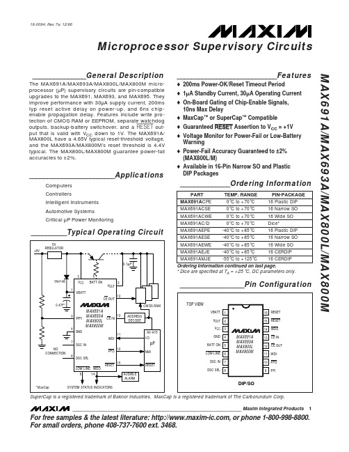
ELECTRICAL CHARACTERISTICS
(MAX691A, MAX800L: VCC = +4.75V to +5.5V, MAX693A, MAX800M: VCC = +4.5V to +5.5V, VBATT = 2.8V, TA = TMIN to TMAX, unless otherwise noted.)
BATT ON 5 LOW LINE 6
OSC IN 7 OSC SEL 8
MAX691A MAX693A MAX800L MAX800M
16 RESET 15 RESET 14 WDO 13 CE IN 12 CE OUT 11 WDI 10 PFO 9 PFI
DIP/SO
SuperCap is a registered trademark of Baknor Industries. MaxCap is a registered trademark of The Carborundum Corp.
元器件交易网
19-0094; Rev 7a; 12/96
Microprocessor Supervisory Circuits
MAX691A/MAX693A/MAX800L/MAX800M
_______________General Description
The MAX691A/MAX693A/MAX800L/MAX800M microprocessor (µP) supervisory circuits are pin-compatible upgrades to the MAX691, MAX693, and MAX695. They improve performance with 30µA supply current, 200ms typ reset active delay on power-up, and 6ns chipenable propagation delay. Features include write protection of CMOS RAM or EEPROM, separate watchdog outputs, backup-battery switchover, and a RESET output that is valid with VCC down to 1V. The MAX691A/ MAX800L have a 4.65V typical reset-threshold voltage, and the MAX693A/MAX800M’s reset threshold is 4.4V typical. The MAX800L/MAX800M guarantee power-fail accuracies to ±2%.
videotec 2015 产品目录中文版说明书

中文产品说明书 2015 CCTV 产品DOCCTZH1507产品说明书 2015 / 修订号 1507所示的全部摄像机和镜头只用于说明, 并非随产品提供 ("ULISSE", "ULISSE COMPACT", "NXPTZ/NXPTZT", "MAXIMUS MPX/MPXT", "MAXIMUS MHX/MHXT", "NTC" 除外)。
如要获取更多信息, 请浏览产品页中的技术数据表。
未经 Videotec S.p.A书面许可, 不得将本文的全部或部分进行复制、修改或记录于文件系统, 以任何形式或者任何电子、机械或记录方式传输。
本文包含的技术规格可能会变更: Videotec S.p.A.保留变更而不事先通知的权利。
技术规格如有变更, 恕不另行通知。
重量和尺寸只作说明用途。
二月 2015. 所有旧版目录均废除。
VIDEOTEC: 辉煌的历史在近三十年,在視頻監控行業的活動,我們設計,創建並獲得專利的眾多產品監測所有類型的外部環境。
今天,我們的公司是一個最受人尊敬的供應商在同行業中,得益於我們的創新,我們的發展CCTV解決方案,保證安全性和可靠性。
遍布全球的销售和技术支持VIDEOTEC的销售和生产总部位于意大利东北部,占地1.3万平方米,另外在法国,美国,加拿大以及亚太地区设立了分部. 迄今为止,VIDEOTEC已经在全球建立了超过100家分销商的营销网络,总的来说,即使面对安防领域最复杂的行业要求,我们也能提供一整套完整的产品选型以及解决方案.产品适合于各种行业我们产品的适用范围非常广泛:从政府部门到国有或私有企业,商业部门,银行以及监狱的视频监控.在这些领域之外还有工业上的应用,比如在高温环境下或特殊的气候环境下,交通控制系统下,城市检测以及海滩和边境系统下,防止某些潜在的爆炸性事件的发生.无与伦比的品质每个VIDEOTEC的解决方案都是由我们的专业人员与国际尖端大学以及研究机构合作后的结果.这种操作模式允许我们作为行业先锋,在实验中用专业的技术以及先进的材料来创造出绝对创新的产品以及解决方案.易安装易维护我们的产品的性能是完美的,并且它的易于安装以及持久稳定性更保证了我门著重于设计的产品理念,这也是我们公司的独特标志,是我们对产品的卓越品质的一份保证.3香港內容9云台摄像机单元防爆云台摄像机单元不锈钢云台摄像机29摄像机外壳隐蔽监视摄像机防护罩防破坏摄像机防护罩防爆摄像机及其防护罩不锈钢摄像机及其防护罩447云台马达不锈钢云台遥测防爆解码器53红外/白光照明灯57视频内容分析63控制键盘矩陣视频分配器67视频传输69摄像机支架5OIL AND GAS市場INDUSTRY PLANTSTERMINALSDRILLING RIGS OIL AND GAS TANKERS PIPELINESOFFSHORE MARINEONSHORE - PERIMETER APPLICATIONSONSHORE - INTERNALAPPLICATIONS OIL AND GAS PLATFORMS67INFRASTRUCTURES AND TRANSPORTATIONCITY SURVEILLANCEBRIDGESPARKING LOTSUNDERGROUNDSAIRPORTSRAILWAYS AND STATIONSHIGHWAYSSTADIUMSTUNNELS8规格如有改变,恕不另行通知。
MAX3095中文资料
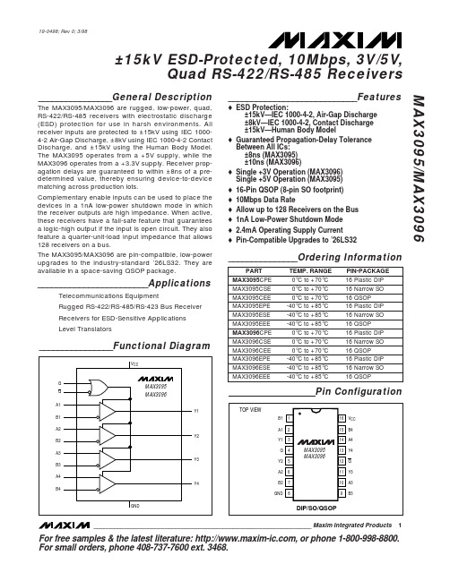
MAX3095/MAX3096
_______________Ordering Information
PART MAX3095CPE MAX3095CSE MAX3095CEE MAX3095EPE MAX3095ESE MAX3095EEE MAX3096CPE MAX3096CSE MAX3096CEE MAX3096EPE MAX3096ESE MAX3096EEE TEMP. RANGE 0°C to +70°C 0°C to +70°C 0°C to +70°C -40°C to +85°C -40°C to +85°C -40°C to +85°C 0°C to +70°C 0°C to +70°C 0°C to +70°C -40°C to +85°C -40°C to +85°C -40°C to +85°C PIN-PACKAGE 16 Plastic DIP 16 Narrow SO 16 QSOP 16 Plastic DIP 16 Narrow SO 16 QSOP 16 Plastic DIP 16 Narrow SO 16 QSOP 16 Plastic DIP 16 Narrow SO 16 QSOP
±15kV ESD-Protected, 10Mbps, 3V/5V, Quad RS-422/RS-485 Receivers MAX3095/MAX3096
ABSOLUTE MAXIMUM RATINGS
Supply Voltage (VCC) ...............................................................7V Control Input Voltage (G, G).......................-0.3V to (VCC + 0.3V) Receiver Input Voltage (A_, B_)...........................................±25V Receiver Output Voltage (Y_).....................-0.3V to (VCC + 0.3V) Continuous Power Dissipation (TA = +70°C) Plastic DIP (derate 10.5mW/°C above +70°C) ............762mW SO (derate 8.7mW/°C above +70°C) ...........................696mW QSOP (derate 8.3mW/°C above +70°C) ......................667mW Operating Temperature Ranges MAX309_C_ _ .....................................................0°C to +70°C MAX309_E_ _...................................................-40°C to +85°C Storage Temperature Range .............................-65°C to +160°C Lead Temperature (soldering, 10sec) .............................+300°C
MAX5939BESA资料

OV UV
MAX5921 MAX5939
6 5
VEE 4
SO
() FOR MAX5921B/F AND MAX5939B/F.
________________________________________________________________ Maxim Integrated Products
MAX5921/MAX5939
Ordering Information
PART MAX5921AESA MAX5921BESA TEMP RANGE -40°C to +85°C -40°C to +85°C PIN-PACKAGE 8Telecom Line Cards Network Switches/Routers Central-Office Line Cards Server Line Cards Base-Station Line Cards
MAX9635中文资料

16-BIT ADC
Байду номын сангаас
6-BIT RANGE DIGITAL
CDR, TIM
SIGNAL
CONTROL PROCESSING
16-BIT ADC
方框图
VCC
SDA SCL I2C AO INT
N
GND
________________________________________________________________ Maxim Integrated Products 1 本文是英文数据资料的译文,文中可能存在翻译上的不准确或错误。如需进一步确认,请在您的设计中参考英文资料。
平板PC/笔记本电脑 TV/投影仪/显示器
数字照明管理 便携设备
蜂窝电话/智能电话
安全系统
应用
业内功耗最低的 环境光传感器,内置ADC
特性
♦♦0.045流明至188,000流明宽检测范围 ♦♦小尺寸、2mm x 2mm x 0.6mm UTDFN-Opto封装 ♦♦VCC = 1.7V至3.6V ♦♦工作电流ICC = 0.65µA ♦♦-40°C至+85°C工作温度范围
由于能够检测极其微弱的光线,非常适合光线较暗的工作 环境。
片上光电二极管的光谱响应针对人眼对环境光的响应进行优 化,集成红外及紫外线屏蔽功能。自适应增益电路可自动选
择正确的流明范围优化测试(计数值 / 流明)。
IC设计工作在1.7V至3.6V供电范围,满负荷工作时仅 消 耗0.65µA电流。器件采用小尺寸2mm x 2mm x 0.6mm UTDFN-Opto封装。
有关价格、供货及订购信息,请联络Maxim亚洲销售中心:10800 852 1249 (北中国区),10800 152 1249 (南中国区), 或访问Maxim的中文网站:。
联盛UT165量产使用手册中文版

Hidden Block Partition: Auto: 量 File System: FAT32 來 Volume Label:
USB 2.0
8
无忧存储论坛
无忧存储网
UT165 MP Tool User’s Manual
flash bad block 連 行 F12 兩 滑 便 行 Format 來 料 參 不 bad block information
”F7” F7 Flash
无忧存储网
量
Version 4.0 AUGUST 13, 2008
All rights strictly reserved. Any portion of this paper shall not be reproduced, copied, or translated to any other forms without permission from Afa Technologies Inc.
歩:
Disk
歩:
1
(
來
)
Save
六歩:
行 MP
Disk
1
(
類
)
7
无忧存储论坛
无忧存储网
UT165 MP Tool User’s Manual 5.
說 :
量 Partition Firmware 量
[Capacity] 不 來 來 [Firmware ID]
USB VID/PID
來
[USB VID/PID]
來
[Inquiry Strings]
[Serial Number] [Write Protect] Yes No 來 Flash Size 粒數 [Flash ID]
MAX6359MSUT-T中文资料

__________Voltage Threshold Levels
PART NO. SUFFIX (_ _) LT LS LR MT MS MR TY SY VCC5 NOMINAL VOLTAGE THRESHOLD (V) 4.63 4.63 4.63 4.38 4.38 4.38 3.08 2.93 VCC3 NOMINAL VOLTAGE THRESHOLD (V) 3.08 2.93 2.63 3.08 2.93 2.63 2.19 2.19
Pin Configurations appear at end of data sheet. Selector Guide appears at end of data sheet.
1
________________________________________________________________ Maxim Integrated Products
MAX6351–MAX6360
Applications
Computers Controllers Portable/Battery-Powered Equipment Intelligent Instruments Multivoltage Systems
PART* MAX6351_ _UT-T MAX6352_ _UK-T MAX6353_ _UK-T MAX6354_ _UK-T MAX6355_ _UT-T MAX6356_ _UT-T MAX6357_ _UT-T MAX6358_ _UT-T MAX6359_ _UT-T MAX6360_ _UT-T
For free samples & the latest literature: , or phone 1-800-998-8800. For small orders, phone 1-800-835-8769.
MIX3015 6.5W 立体声 D 类音频功率放大器说明书

描述MIX3015是一款高效率、无滤波器6.5W 立体声D 类音频放大器。
MIX3015的 差分输入架构和极高的PSRR 有效地提 高了MIX3015对RF 噪声的抑制能力。
防破音功能解决了不同音源输出幅度不一致的问题,同时带来不失真的完美音乐享受。
无需滤波器的PWM 调制结构及增益内置方式减少了外部元件、PCB 面积和系统成本,并简化了设计。
高达90%的效率,快速启动时间和纤小的封装尺寸使得MIX3015成为蓝牙音箱和其他便携式音频产品的最佳选择。
MIX3015具有关断功能,极大的延长系统的待机时间。
过热保护功能增强系统的可靠性。
POP 声抑制功能改善了系统的听觉感受,同时简化系统调试MIX3015提供带散热片的ESOP16封装特性⏹输出功率:-6.5W (VDD=6.0V, RL =2Ω,THD+N=10%) -5.3W (VDD=5.0V, RL =2Ω,THD+N=10%) ⏹ 工作电压 : 2.5V to 6.0V ⏹ 低失真和低噪声 ⏹ 开机POP 声抑制功能 ⏹ 关机电流小于1uA ⏹过热保护功能应用⏹ 蓝牙音箱⏹插卡音箱 / USB 音箱典型应用电路图ON 789OFF管脚排列OUTL+PGNDOUTL-PVDDNCN SHDNBypassINL-INL+OUTR+PGNDOUTR-PVDDAGNDINR-INR+管脚描述管脚符号I/O描述1 OUTL+ O左通道正输出端2,15 PGND 功率地线3 OUTL- O左通道负输出端4,13 PVDD 功率电源5 NCN I防破音控制管脚(高电平为打开防破音)6 Bypass 旁路电容管脚7 INL- I左通道信号负极性输入8 INL+ I左通道信号正极性输入9 INR+ I右通道信号正极性输入10 INR- I 右通道信号负极性输入11 AGND 模拟地线12 SHDN I 系统关断(低电平关机,高电平功放工作)14 OUTR- O右通道负输出端16 OUTR+ O右通道正输出端Shanghai Mixinno Microelectronics Co., Ltd订货信息料号封装表面印字包装MIX3015 ESOP16MIX3015 XXXXXXX2500颗/卷绝对最大额定值V DD 供电电压 -0.3V to 6.3V V I 输入电压 -0.3V to V DD +0.3V T A 工作温度 -40°C to 85°C T J 结温 -40°C to 125°C T STG 储存温度 -65°C to 150°C T SLD焊接温度300°C, 5sec推荐额定值MIN MAX UNITV DD 供电电压 VDD 2.5 6.0 VV IH SHDN高电平 V DD = 5.0V 1.65 V V IL SHDN低电平 V DD = 5.0V 0.6 VV IH NCN高电平 V DD = 5.0V >4/5 VDD V V ILNCN低电平V DD =5.0V< 1/5 VDDV热阻参数Parameter Symbol Package MAX UNIT热阻(Junction to Ambient) θJA ESOP16 90 °C/W 热阻(Junction to Case)θJCESOP16 11 °C/WShanghai Mixinno Microelectronics Co., Ltd电性参数(VDD =5V, Gain=20dB, R L =8Ω, T =25°C, unless otherwise noted.)Symbol Parameter TestConditions MINTYPMAX UNIT V IN电源电压 2.5-6.0V P O输出功率THD+N=10%,f=1KHZ,R L=4ΩV DD=5.0V 3.2WV DD=3.6V 1.6THD+N=1%,f=1KHZ,R L=4ΩV DD=5.0V 2.6WV DD=3.6V 1.3THD+N=10%,f=1KHZ,R L=2ΩV DD=5.0V 5.2WV DD=3.6V 2.6THD+N=1%,f=1KHZ,R L=2ΩV DD=5.0V 4.2WV DD=3.6V 2.2THD+N 总谐波失真+噪声V DD=5.0V, P O=1W, R L=4Ωf=1KHz0.05%V DD=3.6V, P O=0.5W, R L=4Ω0.05V DD=5.0V, P O=2W, R L=2Ωf=1KHz0.06%V DD=3.6V, P O=1W, R L=2Ω0.06G V增益 Ri=22K23.5 dBPSRR 电源纹波抑制比VDD=5.0V ±200mVp-p f=1KHz 65 dB SNR 信噪比V DD=5.0V,Po = 3W, G V=24dB f=1KHz 89 dB Vn 残余噪声V DD=5.0V,Input floating withC IN=0.1μF, Rin=150KA-weighting 110μVNo A-weighting 150 Dyn 动态范围V DD= 5.0V,THD+N=1% f=1KHz 86 dB η效率R L=2Ω, Po=4.5Wf=1KHz85%R L=4Ω, Po=2.5W 90I Q静态电流V DD=5.0VNo Load12mAV DD=3.0V 8I SD关断电流V DD=2.5V to 4.2V V SD=3.3V 1 μAVos 失调电压V IN=0V, V DD=5V 10 mV Fosc 工作频率 350 khz Tst 启动时间Bypass capacitor =1uF 100 mS OTP -No Load, JunctionTemperatureV DD=5.0V200°C OTH - 30Shanghai Mixinno Microelectronics Co., Ltd 典型特征曲线(VDD =5V, Gain=23.6dB, R L =4Ω, T =25°C, unless otherwise noted.)THD+N vs Output Power THD+N vs Output PowerTHD+N VS FREQUENCYCross-TalkNOISE FLOOR FFTFrequency Response20m 100m 500m 1W20k5001k 2k5k Hz-50-85-80-75-70-65-60-55TT TT -120-110-100-90-80d B V1020=4ohm Gain=23.6dB =4ohm Gain=23.6dBShanghai Mixinno Microelectronics Co., Ltd 应用信息输入电阻(Ri)MIX3015的增益由音量调节控制的输入电阻(RI)和反馈电阻RF)控制。
MAX1290中文资料
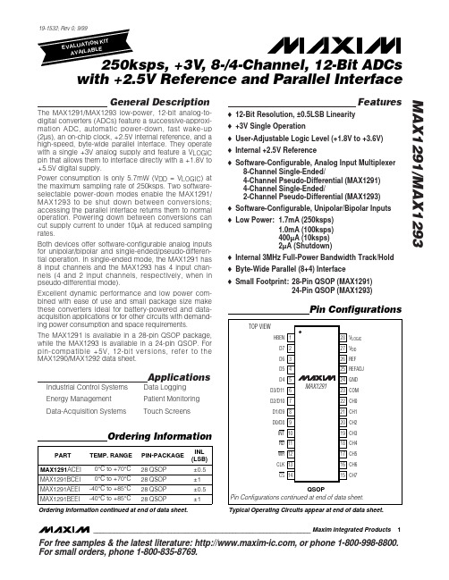
19-1532; Rev 0; 9/99
KIT ATION EVALU E L B AVAILA
250ksps, +3V, 8-/4-Channel, 12-Bit ADCs with +2.5V Reference and Parallel Interface
D4 5 D3/D11 6 D2/D10 7 D1/D9 8 D0/D8 9
MAX1291
23 COM 22 CH0 21 CH1 20 CH2 19 CH3 18 CH4 17 CH5 16 CH6 15 CH7
Ordering Information
PART MAX1291ACEI MAX1291BCEI MAX1291AEEI MAX1291BEEI TEMP. RANGE 0°C to +70°C 0°C to +70°C -40°C to +85°C -40°C to +85°C PIN-PACKAGE 28 QSOP 28 QSOP 28 QSOP 28 QSOP INL (LSB) ±0.5 ±1 ±0.5 ±1
INT 10 RD 11 WR 12 CLK 13 CS 14
QSOP Pin Configurations continued at end of data sheet.
Ordering Information continued at end of data sheet.
Typical Operating Circuits appear at end of data sheet.
元器件交易网
250ksps, +3V, 8-/4-Channel, 12-Bit ADCs with +2.5V Reference and Parallel Interface MAX1291/MAX1293
MAX6339IUT-T中文资料
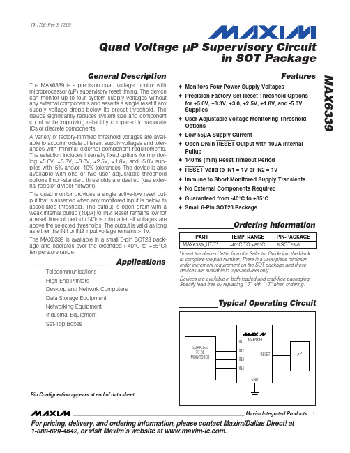
General DescriptionThe MAX6339 is a precision quad voltage monitor with microprocessor (µP) supervisory reset timing. The device can monitor up to four system supply voltages without any external components and asserts a single reset if any supply voltage drops below its preset threshold. The device significantly reduces system size and component count while improving reliability compared to separate ICs or discrete components.A variety of factory-trimmed threshold voltages are avail-able to accommodate different supply voltages and toler-ances with minimal external component requirements.The selection includes internally fixed options for monitor-ing +5.0V, +3.3V, +3.0V, +2.5V, +1.8V, and -5.0V sup-plies with -5% and/or -10% tolerances. The device is also available with one or two user-adjustable threshold options if non-standard thresholds are desired (use exter-nal resistor-divider network).The quad monitor provides a single active-low reset out-put that is asserted when any monitored input is below its associated threshold. The output is open drain with a weak internal pullup (10µA) to IN2. Reset remains low for a reset timeout period (140ms min) after all voltages are above the selected thresholds. The output is valid as long as either the IN1 or IN2 input voltage remains > 1V.The MAX6339 is available in a small 6-pin SOT23 pack-age and operates over the extended (-40°C to +85°C)temperature range.________________________ApplicationsTelecommunications High-End PrintersDesktop and Network Computers Data Storage Equipment Networking Equipment Industrial Equipment Set-Top BoxesFeatures♦Monitors Four Power-Supply Voltages♦Precision Factory-Set Reset Threshold Options for +5.0V, +3.3V, +3.0, +2.5V, +1.8V, and -5.0V Supplies ♦User-Adjustable Voltage Monitoring Threshold Options ♦Low 55µA Supply Current♦Open-Drain RESET Output with 10µA Internal Pullup ♦140ms (min) Reset Timeout Period ♦RESET Valid to IN1 = 1V or IN2 = 1V♦Immune to Short Monitored Supply Transients ♦No External Components Required ♦Guaranteed from -40°C to +85°C ♦Small 6-Pin SOT23 PackageMAX6339Quad Voltage µP Supervisory Circuitin SOT Package________________________________________________________________Maxim Integrated Products 119-1756; Rev 3; 12/05Ordering Information*Insert the desired letter from the Selector Guide into the blank to complete the part number. There is a 2500 piece minimum order increment requirement on the SOT package and these devices are available in tape-and-reel only.Devices are available in both leaded and lead-free packaging.Specify lead-free by replacing “-T” with “+T” when ordering.Pin Configuration appears at end of data sheet.Typical Operating CircuitFor pricing, delivery, and ordering information,please contact Maxim/Dallas Direct!at 1-888-629-4642, or visit Maxim’s website at .M A X 6339Quad Voltage µP Supervisory Circuit in SOT Package 2_______________________________________________________________________________________ABSOLUTE MAXIMUM RATINGSStresses beyond those listed under “Absolute Maximum Ratings” may cause permanent damage to the device. These are stress ratings only, and functional operation of the device at these or any other conditions beyond those indicated in the operational sections of the specifications is not implied. Exposure to absolute maximum rating conditions for extended periods may affect device reliability.Terminal Voltage (with respect to GND)Input Voltages (IN_ ) (except -5V)............................-0.3V to +6V RESET .......................................................................-0.3V to +6V Input Voltage (-5V Input)..........................................-6V to +0.3V Continuous RESET Current.................................................20mA Continuous Power Dissipation (T A = +70°C)6-pin SOT23 (derate 8.7mW/°C above +70°C).........695.7mWOperating Temperature Range ...........................-40°C to +85°C Storage Temperature Range.............................-65°C to +150°C Junction Temperature......................................................+150°C Lead Temperature (soldering, 10s).................................+300°CELECTRICAL CHARACTERISTICS(V = +1V to +5.5V, T = -40°C to +85°C, unless otherwise noted. Typical values are at V = +3.0V to +3.3V, T = +25°C, unlessMAX6339Quad Voltage µP Supervisory Circuitin SOT Package_______________________________________________________________________________________3ELECTRICAL CHARACTERISTICS (continued)(V IN2= +1V to +5.5V, T A = -40°C to +85°C, unless otherwise noted. Typical values are at V IN2= +3.0V to +3.3V, T A = +25°C, unless otherwise noted.) (Note 1)Note 1:100% production tested at T A = +25°C. Limits over temperature guaranteed by design.Note 2:The device is powered from input IN2.Note 3:The RESET output is guaranteed to be in the correct state for IN1 or IN2 down to 1V.Note 4:Monitored voltage (+3.3V, +3.0V) is also the device power supply. Supply current splits as follows: 25µA for the resistor- divider (for the monitored voltage) and 30µA for other circuits.3550454055606570758085-40-2020406080I IN2 INPUT CURRENT vs. TEMPERATURETEMPERATURE (°C)I I N 2 I N P U T C U R R E N T (µA )50605570658075853.04.03.54.55.05.5I IN2 INPUT CURRENT vs. I IN2 VOLTAGEM A X 6339t o c 02INPUT VOLTAGE (V)I I N 2 I N P U T C U R R E N T (µA )-0.30-0.15-0.20-0.25-0.10-0.500.050.100.15-40-2020406080NORMALIZED THRESHOLD ERRORvs. TEMPERATURETEMPERATURE (°C)N O R M A L I Z E D T H R E S H O L D E R R O R (%)Typical Operating Characteristics(V IN2= +3.0V, T A = +25°C)Pin DescriptionM A X 6339Quad Voltage µP Supervisory Circuit in SOT Package Typical Operating Characteristics (continued)(VIN2= +3.0V, T A = +25°C)180190185195200205210215-40-2020406080RESET TIMEOUT DELAY vs. TEMPERATUREM A X 6339t o c 07TEMPERATURE (°C)R E S E T T I M E O U T D E L A Y (m s )RESET 2V/divIN_2V/div200ms/divRESET TIMEOUT DELAYM A X 6339t o c 082V/div201030607050408002003004005001006007008009001000MAXIMUM IN_ TRANSIENT DURATION vs. RESET THRESHOLD OVERDRIVERESET THRESHOLD OVERDRIVE (mV)M A X I M U M I N _ T R A N S I E N T D U R A T I O N (µs )201030607050408002003004005001006007008009001000RESET DELAY vs. RESET THRESHOLDOVERDRIVE (IN_ decreasing)M A X 6339t o c 05RESET THRESHOLD OVERDRIVE (mV)R E S E T D E L A Y (µs )RESET 2V/divIN_100mV/div10µs/divRESET PULLUP AND PULLDOWNRESPONSE (C L = 47pF)M A X 6339t o c 06MAX6339Quad Voltage µP Supervisory Circuitin SOT Package_______________________________________________________________________________________5Detailed DescriptionThe MAX6339 is a very small, low-power, quad voltage µP supervisory circuit designed to maintain system integrity in multi-supply systems (Figure 1). The device offers several internally trimmed undervoltage threshold options that minimize or eliminate the need for external components. Preset voltage monitoring options for +5.0V, +3.3V, +3.0V, +2.5V, +1.8V, and -5.0V make it ideal for telecommunications, desktop and notebook computers, high-end printers, data storage equipment,and networking equipment applications.The quad monitor/reset includes an accurate bandgap reference, four precision comparators, and a series of internal trimmed resistor-divider networks to set the fac-tory-fixed reset threshold options. The resistor networks scale the specified IN_ reset voltages to match the internal bandgap reference/comparator voltage. User-adjustable threshold options bypass the internal resis-tor networks and connect directly to one of the comparator inputs (an external resistor-divider network is required for threshold matching). All threshold volt-age options, fixed and adjustable, are indicated through a single-letter code in the product number (see the Selector Guide ).Each of the internal comparators has a typical hystere-sis of 0.3% with respect to its reset threshold. This built-in hysteresis improves the monitor’s immunity to ambient noise without significantly reducing threshold accuracy when an input sits at its specified reset volt-age. The MAX6339 is also designed to ignore short IN_transients. See the Typical Operating Characteristics for a glitch immunity graph.Applications InformationReset OutputThe MAX6339 RESET output is asserted low when any of the monitored IN_ voltages drop below its specified reset threshold (or above for -5V option) and remain low for the reset timeout period (140ms minimum) after all inputs exceed their thresholds (Figure 2). The output is open drain with a weak internal pullup to the moni-tored IN2 supply (10µA typ). For many applications no external pullup resistor is required to interface with other logic devices. An external pullup resistor to any voltage from 0 to +5.5V can overdrive the internal pullup if interfacing to different logic supply voltages (Figure 3). Internal circuitry prevents reverse current flow from the external pullup voltage to IN2.The MAX6339 is normally powered from the monitored IN2 supply when all input voltages are above their specified thresholds. When any supply drops below itsthreshold, the reset output is asserted and guaranteed to remain low while either IN1 or IN2 is above +1.0V.User-Adjustable ThresholdsThe MAX6339 offers several monitor options with user-adjustable reset thresholds. The threshold voltage at each adjustable IN_ input is typically 1.23V. To monitor a voltage > 1.23V, connect a resistor-divider network to the circuit as shown in Figure 4.V INTH = 1.23V x (R1 + R2) / R2or, solved in terms of R1:R1 = R2 ((VI NTH / 1.23V) - 1)Because the MAX6339 has a guaranteed input current of ±0.1µA on its adjustable inputs, resistor values up to 100k Ωcan be used for R2 with < 1% error.Unused InputsIf some monitor inputs are to be unused, they must be tied to a supply voltage greater in magnitude than their specified threshold voltages. For unused IN3 or IN4options with positive thresholds (fixed or adjustable),the inputs can be connected directly to the IN2 supply.For unused IN4 options with negative thresholds, the input must be tied to a more negative supply. The IN2input must always be used for normal operation (device power-supply pin). Unused pins cannot be connected to ground or allowed to float.Negative Voltage Monitoring Beyond -5VThe MAX6339 is offered with options to monitor -5V sup-plies with internally fixed thresholds. To monitor supplies more negative than -5V, a low-impedance resistor-divider network can be used external to the MAX6339 as shown in Figure 5. The current through the external resis-tor-divider should be greater than the input current for the -5V monitor options. For an input monitor current error of < 1%, the resistor-divider current should ≥ 2mA (for I IN4= 20µA max). Set R2 = 2.5k Ω. Calculate R1based on the desired V IN_reset threshold voltage, using the following formula:R1 = R2 ✕[(V INTH / V TH ) -1]where R2 ≤2.49k Ω, V INTH = desired threshold voltage and V TH is the internal threshold voltage.M A X 6339Quad Voltage µP Supervisory Circuit in SOT Package 6_______________________________________________________________________________________Figure 1. Functional DiagramMAX6339Quad Voltage µP Supervisory Circuitin SOT Package_______________________________________________________________________________________7For -V IN = -12V nominal, VI NTH = -11.1V, V TH = -4.63V,and R2 = 2.49k Ω,R1 = 2.49k Ω✕[(-11.1 / -4.63) -1]R1 = 3.48k ΩPower-Supply Bypassing and GroundingThe MAX6339 is normally powered from the monitored IN2 supply input. All monitor inputs are immune to short supply transients. If higher immunity is desired in noisy applications, connect 0.1µF bypass capacitors from the IN2 input to ground. Additionally, capacitance can be added to IN1, IN3, and IN4 to increase their noise immunity.Chip InformationTRANSISTOR COUNT: 896PROCESS: BiCMOSFigure 4. Setting the Auxiliary MonitorM A X 6339Quad Voltage µP Supervisory Circuit in SOT Package 8_______________________________________________________________________________________Maxim cannot assume responsibility for use of any circuitry other than circuitry entirely embodied in a Maxim product. No circuit patent licenses are implied. Maxim reserves the right to change the circuitry and specifications without notice at any time.Maxim Integrated Products, 120 San Gabriel Drive, Sunnyvale, CA 94086 408-737-7600_____________________9©2005 Maxim Integrated Productsis a registered trademark of Maxim Integrated Products, Inc.6L S O T .E P SMAX6339Quad Voltage µP Supervisory Circuitin SOT PackagePackage Information(The package drawing(s) in this data sheet may not reflect the most current specifications. For the latest package outline information,go to /packages .)。
TVFS9说明书V1.2(2011年版)

符号约定 注意 由于没有按要求操作,可能造成中等程度伤害或轻伤的场合。
危险 由于没有按要求操作,可能造成死亡或重伤的场合。
-2-
TVFS9 系列高性能通用变频器使用说明书
01hz5000hz点动加减速时间013600秒tvfs9系列高性能通用变频器使用说明书内置pid可方便地构成闭环控制系统适用于压力流量等过程控制多段速运行通过内置plc或控制端子实现多段速运行纺织摆频自动电压调整当电网电压变化时调节pwm输出保持输出电压的恒定avr功能自动节能运行根据负载情况自动优化vf曲线实现节能运行自动限流对运行期间电流自动限制防止频繁过流故障跳闸转矩特性1hz时输出额定转矩的150转速稳定精度01矢量控制电机参数自辨识可在电机完全静止的情况下完成电机参数的自辨识以获得最佳控制效果运行命令通道操作面板给定
-3-
TVFS9 系列高性能通用变频器使用说明书
第六章 功能参数表详述 6.1 基本运行参数(P0.00-P0.23)---------------------(56) 6.2 电机与矢量控制参数(P1.00-P1.15)------------(66) 6.3 辅助运行参数(P2.00-P2.43)---------------------(69) 6.4 用户管理界面参数(P3.00-P3.09)---------------(77) 6.5 开关量输入输出参数(P4.00-P4.16)------------(79) 6.6 模拟输入输出参数(P5.00-P5.16)---------------(88) 6.7 过程 PID 控制参数(P6.00-P6.14)---------------(93) 6.8 可编程运行参数(P7.00-P7.18)------------------(100) 6.9 通讯参数(P8.00-P8.04)---------------------------(105) 6.10 保护参数(P9.00-P9.03)--------------------------(107) 6.11 高级功能参数(PA.00-PA.06)-------------------(109)
TV009规格
iPlayer TV009 SD/USB 媒体播放器产品信息:iPlayer TV009 SD/USB媒体播放器, 她能读SD/USB上的多媒体文件,并且进行解码,通过VGA接口输出到电脑显示器和投影机,通过A V(RCA)接口输出到电视机,安装非常简单,插上适配器电源就可以用。
iPlayer支持JPEG图片文件,MP3/WMA音乐文件,MPEG1/MPEG2/ MPEG4格式电影文件.iPlayer是一台没有伺服的DVD播放器, iPlayer是一台没有屏的数码相框. iPlayer是一台SD/USB代替硬盘的硬盘播放器.另外iPlayer也可以当着一台广告机...等等.您可以在电视上看互联网的内容,并且免费获得转换软件"3GP-Video-Converter",可以到我们网站上下载(/Download.asp)详细资料:关键点:B接口超强的适应能力,延长15米都可以正常播放USB里的内容;(任何其他方案都没办法做到)....解大码率的.vob文件不会有任何停顿等不流畅的问题....低功耗,主控不发烫....开机自动播放,支持热拔插….支持断电记忆,断电记忆(拔掉设备,再插入会自动记忆播放)....支持中文文件名….自动幻灯模式播放图片;....图片旋转: 90°, 180°, 270°..支持放大缩小..支持媒体格式图片: JPEG声音: MP3 and WMA files视频: MPEG1, MPEG2,MPEG4,divx,xvid(.dat.avi.vob.mpg.mpeg)规格:符合USB2.0规范.支持NTSC, PAL视频输出:CVBS复合视频输出(RCA),VGA输出音频输出: 立体声音频输出(RCA)裸机尺寸: (L)120mm x (W)120mm x (H)25mm包装组件:iPlayer SD/USB 媒体播放器A V 线说明书遥控器5V(1A)电源适配器Model No.: TV009。
- 1、下载文档前请自行甄别文档内容的完整性,平台不提供额外的编辑、内容补充、找答案等附加服务。
- 2、"仅部分预览"的文档,不可在线预览部分如存在完整性等问题,可反馈申请退款(可完整预览的文档不适用该条件!)。
- 3、如文档侵犯您的权益,请联系客服反馈,我们会尽快为您处理(人工客服工作时间:9:00-18:30)。
MAX6351–MAX6360
__________Voltage Threshold Levels
PART NO. SUFFIX (_ _) LT LS LR MT MS MR TZ TY TW TV SZ SY SW VCC1 NOMINAL VOLTAGE THRESHOLD (V) 4.63 4.63 4.63 4.38 4.38 4.38 3.08 3.08 3.08 3.08 2.93 2.93 2.93 VCC2 NOMINAL VOLTAGE THRESHOLD (V) 3.08 2.93 2.63 3.08 2.93 2.63 2.32 2.19 1.67 1.58 2.32 2.19 1.67
Dual/Triple-Voltage µP Supervisory Circuits MAX6351–MAX6360
ABSOLUTE MAXIMUM RATINGS
VCC1, VCC2 to GND .................................................-0.3V to +6V RST (MAX6352/MAX6355/MAX6358)...................... -0.3V to +6V RST, MR, WDI, RST1, RSTIN (MAX6351/MAX6353/ MAX6356/MAX6359) ..............................-0.3V to (VCC1 + 0.3V) RST, RST2 (MAX6351/MAX6354/ MAX6357/MAX6360) ..............................-0.3V to (VCC2 + 0.3V) Input/Output Current, All Pins .............................................20mA Continuous Power Dissipation (TA = +70°C) 5-Pin SOT23 (derate 7.1mW/°C above +70°C)............571mW 6-Pin SOT23 (derate 8.7mW/°C above +70°C)............695mW Operating Temperature Range ...........................-40°C to +85°C Junction Temperature .....................................................+150°C Storage Temperature Range .............................-65°C to +150°C
ห้องสมุดไป่ตู้
Features
♦ Precision Monitoring of Multiple +1.8V, +2.5V, +3.0V, +3.3V, and +5V Power-Supply Voltages ♦ Precision Factory-Set Power-Supply Reset Thresholds ♦ 20µA Supply Current ♦ 100ms min Power-On Reset Pulse Width ♦ Debounced TTL/CMOS-Compatible Manual-Reset Input ♦ Watchdog Timer 46.4s Startup Timeout 2.9s Normal Timeout ♦ Fully Guaranteed Over Temperature ♦ Guaranteed RESET Valid to VCC1 = 1V or VCC2 = 1V ♦ Power-Supply Transient Immunity ♦ No External Components for Dual-Voltage Systems ♦ Small 5- and 6-Pin SOT23 Packages ♦ Low Cost
For pricing, delivery, and ordering information, please contact Maxim/Dallas Direct! at 1-888-629-4642, or visit Maxim’s website at .
元器件交易网
元器件交易网
19-1508; Rev 6; 12/05
Dual/Triple-Voltage µP Supervisory Circuits
General Description
The MAX6351–MAX6360 microprocessor (µP) supervisors with multiple reset voltages significantly improve system reliability and accuracy compared to separate ICs or discrete components. If any input supply voltage drops below its associated preset threshold, all reset outputs are asserted. In addition, the outputs are valid as long as either input supply voltage remains greater than +1.0V. All devices in this series have an active-low debounced manual reset input. In addition, the MAX6358/MAX6359/ MAX6360 offer a watchdog-timer input with a 46.4s startup timeout period and a 2.9s timeout period. The MAX6355/MAX6356/MAX6357 offer an additional voltage monitor input to monitor a third voltage. The MAX6351 features two active-low, push-pull reset outputs, one is referenced to VCC1 and the other is referenced to VCC2. The MAX6353/MAX6356/MAX6359 offer an active-low, push-pull reset output referenced to VCC1. The MAX6354/MAX6357/MAX6360 offer an active-low, push-pull reset output referenced to VCC2. All these devices are offered with a wide variety of voltage threshold levels, as shown in the Voltage Threshold Levels table. They are available in 5- and 6-pin SOT23 packages and operate over the extended (-40°C to +85°C) temperature range.
Stresses beyond those listed under “Absolute Maximum Ratings” may cause permanent damage to the device. These are stress ratings only, and functional operation of the device at these or any other conditions beyond those indicated in the operational sections of the specifications is not implied. Exposure to absolute maximum rating conditions for extended periods may affect device reliability.
Applications
Computers Controllers Portable/Battery-Powered Equipment Intelligent Instruments Multivoltage Systems
Ordering Information
PART* MAX6351_ _UT-T MAX6352_ _UK-T MAX6353_ _UK-T MAX6354_ _UK-T MAX6355_ _UT-T MAX6356_ _UT-T MAX6357_ _UT-T TEMP RANGE -40°C to +85°C -40°C to +85°C -40°C to +85°C -40°C to +85°C -40°C to +85°C -40°C to +85°C -40°C to +85°C PIN-PACKAGE 6 SOT23-6 5 SOT23-5 5 SOT23-5 5 SOT23-5 6 SOT23-6 6 SOT23-6 6 SOT23-6
MAX6358_ _UT-T -40°C to +85°C 6 SOT23-6 MAX6359_ _UT-T -40°C to +85°C 6 SOT23-6 MAX6360_ _UT-T -40°C to +85°C 6 SOT23-6 SV 2.93 1.58 * The _ _ are placeholders for the threshold voltage levels of the UW 2.78 1.67 devices. Substitute the part number suffix in the Voltage ThresUV 2.78 1.58 hold Levels table for the desired voltage level. All devices are available in tape-and-reel only. There is a 2500 piece minimum RW 2.63 1.67 order increment for the SOT package. RV 2.63 1.58 Devices are available in both leaded and lead-free packaging. Note: Standard versions are shown in bold. Sample stock is genSpecify lead-free by replacing “-T” with “+T” when ordering. erally held on the standard versions only. Contact factory for availPin Configurations appear at end of data sheet. ability. Selector Guide appears at end of data sheet. ________________________________________________________________ Maxim Integrated Products 1
