R4ABLKBLKFF0;中文规格书,Datasheet资料
RX424024中文资料

V REG.-Nr. A651, Z E214025Contact dataContact configuration 2 COContact setsingle contact Type of interruption micro disconnectionRated current8ARated voltage / max.switching voltage AC 240/400VAC Maximum breaking capacity AC2000VA Limiting making capacity, max 4 s, duty factor 10%15A Contact materialAgNi 90/106AC coil> 1 x 10⁶cycles Rated frequency of operation with / without load 6 / 600 min -1Contact ratings Type Load Cycles RX48A, 250VAC, 70°C, EN61810-14x104RX48A, 250VAC, 70°C, UL508 General purpose4x104Coil dataAC coil24...230VAC AC coiltyp 0,75VAOperative range2Coil insulation system according UL1446class FCoil versions,DC-coil Coil Rated Operate Release Coil Rated coil code voltage voltage voltage resistance powerVDC VDC VDC Ohm mW0055 3.50.550+10%5000066 4.20.668+10%529012128.4 1.2274+10%5260242416.8 2.41095+10%5260484833.6 4.84380+10%5260606042.0 6.06845+10%52611011077.011.023010+10%526All figures are given for coil without preenergization, at ambient temperature +23°CS0271-ACoil versions,AC-coil 50HzCoil Rated Operate Release Coil Rated coil code voltage voltage voltage resistance power50Hz50Hz50Hz VAC VAC VAC Ohm VA 5242418.0 3.6350+10%0.76 61511586.317.38100+15%0.76 730230172.534.532500+15%0.74 All figures are given for coil without preenergization, at ambient temperature +23°C Insulationrmsopen contact circuit1000 V rmsadjacent contact circuits2500 V rmsClearance/creepage coil-contact circuit W8 / 8 mmadjacent contact circuits W3 / 4 mmMaterial group of insulation parts W IIIaTracking index of relay base PTI 250 VInsulation to IEC 60664-1Type of insulation coil-contact circuit reinforcedopen contact circuit functionaladjacent contact circuits basicRated insulation voltage250 VPollution degree32Rated voltage system 240V400VOvervoltage category IIIOther dataRoHS - Directive 2002/95/EC compliant as per product date code 0413 Flammability class according to UL94 V-0 1)Ambient temperature range-40...+70°COperate- / release time DC coil typ 7 / 2msBounce time DC coil, NO / NC contact typ 1 / 3msVibration resistance (function) NO / NC contact20 / 4g, 10 ... 150 HzShock resistance (destruction) 100 gCategory of protection RTII - flux proof transparent version pcbMounting distance 2,5 mm 2)Resistance to soldering heat flux-proof version270°C / 10 sRelay weight14 gPackaging unit500 pcs12) Version with transparent cover: 5 mmAccessoriesFor standard version (white cover), details seeaccessories RT PCB layout / terminal assignmentBottom view on solder pinsS0163-BJDimensionsS0272-BA *) With the recommended PCB hole sizes a grid pattern from 2.5mm to 2.54mm can be used.。
IRG4PC40KPBF;中文规格书,Datasheet资料

VCC = 80%(VCES), VGE = 20V, L = 10µH, RG = 10Ω,
(See fig. 13a)
Pulse width ≤ 80µs; duty factor ≤ 0.1%. Pulse width 5.0µs, single shot.
2
TO-247AC
Max.
600 42 25 84 84 10 ±20 15 160 65 -55 to +150 300 (0.063 in. (1.6mm) from case) 10 lbfin (1.1Nm)
Units
V A
µs V mJ W
°C
Thermal Resistance
Parameter
Repetitive rating; VGE = 20V, pulse width limited by
max. junction temperature. ( See fig. 13b )
Repetitive rating; pulse width limited by maximum
junction temperature.
TC , Case Temperature ( ° C)
TJ , Junction Temperature ( ° C)
Fig. 4 - Maximum Collector Current vs. Case Temperature
Fig. 5 - Typical Collector-to-Emitter Voltage vs. Junction Temperature
Switching Characteristics @ TJ = 25°C (unless otherwise specified)
nRF24L01P产品说明书V1.0资料
nRF24L01+单片机2.4 GHz收发器产品说明书v1.0主要功能:全球通用的2.4 GHz ISM波段操作250kbps, 1Mbps and 2Mbps空中数据传输速率超低功率运行发射功率为0dBm(1.0mW)时,发射电流为11.3mA2Mbps空中数据传输速率,接收电流为13.5mA掉电电流为900nA待机-I电流26μA片内电压调整器1.9至3.6V电源供电范围增强型ShockBurst TM自动数据包处理自动包数据包事务处理6数据通道的MultiCeiver TM与nRF24L01嵌入式兼容空中数据速率250kbps 和1Mbps,与nRF2401A,nRF2402, nRF24E1和nRF24E2兼容低BOM成本±60ppm 16MHz晶振容许5V输入紧凑的20引脚4x4mm QFN封装应用无线 PC外围设备鼠标,键盘和遥控器三和一桌面捆绑先进的媒体中心遥控器网络电话耳机游戏控制器蓝牙模块运动手表和传感器消费电子产品射频遥控器家庭和商业自动化超低功率无线传感器网络RFID 射频识别资产跟踪系统玩具免责条款北欧半导体ASA有权做出随时更改,提高产品可靠性、功能或设计,不另行通知。
北欧半导体ASA不承担由于应用程序或使用任何所述产品或电路引起的责任。
所有应用程序的信息咨询,不构成说明书的组成部分。
极限值超过一个或多个限制的应力可能会造成设备永久性损坏。
这些应力等级只有在这样或那样的操作环境中提出,在规范中没有给出。
长时间暴露在限制值附近可能会影响设备的可靠性。
生命支持应用这些产品并非为因故障会引起人身伤害的维生装备,设备或系统设计的。
北欧半导体ASA客户使用或出售这些产品,他们将自担风险并同意完全赔偿北欧半导体ASA因使用不当或销售行为造成任何损害。
详细联系方式访问www.nordicsemi.no进入北欧半导体销售办事处和全世界的分销商网站总办公室:Otto Nielsens vei 127004 Trondheim电话: +47 72 89 89 00传真: +47 72 89 89 89www.nordicsemi.no写作惯例本产品规范遵循一套排版规则,文档一致,容易阅读。
OPA404KU,OPA404KP,OPA404KU 1K,OPA404KU 1KE4,OPA404KUG4,OPA404AG,OPA404BG, 规格书,Datasheet 资料
KP, KU Operating
KP, KU Storage
KP, KU θ Junction-Ambient
KP, KU
IO = 0mADC Ambient Temperature Ambient Temperature Ambient Temperature
© 1986 Burr-Brown Corporation
PDS-677F
Printed in U.S.A. August 1995
芯天下--/
SPECIFICATIONS
ELECTRICAL
At VCC = ±15VDC and TA = +25°C unless otherwise noted.
®
OPA404
2
芯天下--/
ELECTRICAL (FULL TEMPERATURE RANGE SPECIFICATIONS)
At VCC = ±15VDC and TA = TMIN to TMAX unless otherwise noted.
OPA404AG, KP, KU
8
0.5
12
1013 || 1 1014 || 3
±10.5 88 84
+13, –11 100 100
88
100
4
6.4
570
24
35
0.6
1.5
±11.5 +13.2, –13.8
±5
±10
80
1000
±10
±27
±40
±15
±5
±18
9
10
–25
R3000-TP;中文规格书,Datasheet资料
R2500F THRU R3000F200 Milliamp HighVoltage Fast RecoverySilicon Rectifier 2500 to 3000 VoltsFeatures• High Voltage • Low Leakage• Fast Switching For Higher Efficiency • High Current CapabilityMaximum Ratings• Operating Temperature: -55°C to +150°C •Storage Temperature: -55°C to +150°CMicrosemi Catalog Number DeviceMarking MaximumRecurrent Peak Reverse Voltage Maximum RMS Voltage Maximum DC Blocking Voltage R2500F R2500F 2500V 1750V 2500V R3000 FR3000 F 3000V2100V 3000VElectrical Characteristics @ 25°C Unless Otherwise SpecifiedAverage Forward CurrentI F(AV)200mA T A = 50°C Peak Forward Surge Current I FSM30A8.3ms, half sineMaximum DCReverse Current At Rated DC Blocking VoltageI R 5.0µA 50µA T A = 25°C T A = 100°C Typical Junction CapacitanceC J 30pF Measured at1.0MHz, V R =4.0VMaximum Reverse Recovery TimeT rr500nSomp onents 20736 Marilla Street Chatsworth! "# $ % ! "#Maximum Instantaneous Forward VoltageR2500F R3000F V F4.0V5.0V I FM = 0.5A;T A = 50°C TMMicro Commercial Componentswww.mccsemi .com• Lead Free Finish/Rohs Compliant (Note1) ("P"Suffix designatesCompliant. See ordering information) Note: 1. High Temperature Solder Exemptions Applied, see EU Directive Annex 7.• Epoxy meets UL 94 V-0 flammability rating • Moisture Sensitivity Level 1R2500F - R3000F110040510158Figure 3Peak Forward Surge Current Peak Forward Surge Current - Amperes versus Number Of Cycles At 60Hz - CyclesAmpsCycles261020608040202530Average Forward Rectified Current - Amperes versus Ambient Temperature - °CFigure 2Forward Derating Curve15025507510050100150Single Phase, Half Wave60Hz Resistive or Inductive Load mA°C125200250300Instantaneous Reverse Current - Micro Amps versus Percent Of Rated Peak Reverse Voltage - VoltsFigure 1Typical Reverse Characteristics 012020406080.01.02.04.06T J = 25°CµAVolts100.08.1.2.4.6.8124Micro Commercial ComponentsTMwww.mccsemi .comMicro Commercial ComponentsOrdering Information :Device PackingPart Number-TP Tape&Reel: 4Kpcs/ReelPart Number-AP Ammo Packing: 3Kpcs/Ammo BoxPart Number-BP Bulk: 25Kpcs/Carton***IMPORTANT NOTICE***Micro Commercial Components Corp. reserve s the right to make changes without further notice to any product herein to make corrections, modifications , enhancements , improvements , or other changes . Micro Commercial Components Corp . does not assume any liability arising out of the application or use of any product described herein; neither does it convey any license under its patent rights ,nor the rights of others . The user of products in such applications shall assume all risks of such use and will agree to hold Micro Commercial Components Corp . and all the companies whose products are represented on our website, harmless against all damages.***LIFE SUPPORT***MCC's products are not authorized for use as critical components in life support devices or systems without the express writtenapproval of Micro Commercial Components Corporation.***CUSTOMER AWARENESS***Counterfeiting of semiconductor parts is a growing problem in the industry. Micro Commercial Components (MCC) is taking strong measures to protect ourselves and our customers from the proliferation of counterfeit parts. MCC strongly encourages customers to purchase MCC parts either directly from MCC or from Authorized MCC Distributors who are listed by country on our web page cited below. Products customers buy either from MCC directly or from Authorized MCC Distributors are genuine parts, have full traceability, meet MCC's quality standards for handling and storage. MCC will not provide any warranty coverage or other assistance for parts bought from Unauthorized Sources. MCC is committed to combat this global problem and encourage our customers to do their part in stopping this practice by buying direct or from authorized distributors.分销商库存信息: MICRO-COMMERICAL-CO R3000-TP。
BLF2022-40中文资料

DISCRETE SEMICONDUCTORS
DATA SHEET
M3D750
BLF2022-40 UHF power LDMOS transistor
Preliminary specification 2001 April 05
元器件交易网
1
BLF2022-40
PINNING PIN 1 2 3 drain gate source, connected to flange DESCRIPTION
APPLICATIONS • Common source class-AB operation for PCN and PCS applications in the 2000 to 2200 MHz frequency range • Suitable for GSM, Edge, CDMA and WCDMA applications. DESCRIPTION Silicon N-channel enhancement mode lateral D-MOS transistors encapsulated in a 2-lead SOT608A flange package with a ceramic cap. The common source is connected to the mounting flange. Fig.1 Simplified outline SOT608A.
SOT608A
Package under development
D
Philips Semiconductors reserves the right to make changes without notice.
A F
3
HW004A0A1-SZ;中文规格书,Datasheet资料

* UL is a registered trademark of Underwriters Laboratories, Inc. † CSA is a registered trademark of Canadian Standards Association. ‡ VDE is a trademark of Verband Deutscher Elektrotechniker e.V.
** ISO is a registered trademark of the International Organization of Standards
Document No: DS03-017 ver.1.22 PDF No: hw-hc_4-6a.pdf
/
Data Sheet October 5, 2009
HW/HC004/005/006 Series DC-DC Power Module: 18-36Vdc & 36-75Vdc Input; 1.0V-5Vdc Output; 4A - 6A Output Current
Absolute Maximum Ratings
Stresses in excess of the absolute maximum ratings can cause permanent damage to the device. These are absolute stress ratings only, functional operation of the device is not implied at these or any other conditions in excess of those given in the operations sections of the data sheet. Exposure to absolute maximum ratings for extended periods can adversely affect the device reliability.
VLF4012AT-4R7M1R1;VLF4012AT-100MR79;VLF4012AT-3R3M1R3;VLF4012AT-2R2M1R5;中文规格书,Datasheet资料
Inductance tolerance(%) ±30 ±20 ±20 ±20 ±20 ±20 ±20
Test frequency (kHz) 100 100 100 100 100 100 100
DC resistance( ) max. 0.054 0.1 0.15 0.2 0.31 0.46 1.20 typ. 0.047 0.091 0.13 0.1R7
2.8±0.2
1.4max. Dimensions in mm
RECOMMENDED PC BOARD PATTERN
1.2 2.1 3.4 Dimensions in mm
Inductance [at 1/2 Idc1]3 (µH) 1 2.2 3.3 4.7 6.8 10 22
• All specifications are subject to change without notice.
/
001-04 / 20120310 / e531_vlf
(3/17)
Inductors for Power Circuits Wound/STD • Magnetic Shielded
Part No. VLF3014AT-1R0N1R7 VLF3014AT-2R2M1R2 VLF3014AT-3R3M1R0 VLF3014AT-4R7MR90 VLF3014AT-6R8MR72 VLF3014AT-100MR59 VLF3014AT-220MR37
1
SHAPES AND DIMENSIONS
VLF-MT Series VLF302510MT
With the VLF302510MT Series, a DC to DC converter with topclass voltage conversion efficiency for similar size products was achieved by optimizing the magnetic material and configuration. These products are optimal for use as choke coils in switching power supplies such as those in mobile devices requiring spacesaving design. FEATURES • Miniature size Mount area: 3.02.5mm Low profile: 1.0mm max. height • Generic use for portable DC to DC converter line. • High magnetic shield construction should actualize high resolution for EMC protection. • The products contain no lead and also support lead-free soldering. • The products is halogen-free. • It is a product conforming to RoHS directive. APPLICATIONS Smartphones, cellular phones, DSCs, DVCs, HDDs, LCD displays, compact power supply modules, etc. SHAPES AND DIMENSIONS
IRLIZ44NPBF;中文规格书,Datasheet资料
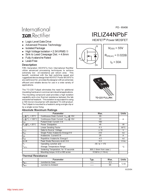
IRLIZ44NPbFHEXFET ® Power MOSFETPD - 95456lLogic-Level Gate Drivel Advanced Process Technology l Isolated Packagel High Voltage Isolation = 2.5KVRMS l Sink to Lead Creepage Dist. = 4.8mm l Fully Avalanche Rated l Lead-FreeFifth Generation HEXFETs from International Rectifier utilize advanced processing techniques to achieve extremely low on-resistance per silicon area. This benefit, combined with the fast switching speed and ruggedized device design that HEXFET Power MOSFETs are well known for, provides the designer with an extremely efficient and reliable device for use in a wide variety of applications.The TO-220 Fullpak eliminates the need for additional insulating hardware in commercial-industrial applications.The moulding compound used provides a high isolation capability and a low thermal resistance between the tab and external heatsink. This isolation is equivalent to using a 100 micron mica barrier with standard TO-220 product.The Fullpak is mounted to a heatsink using a single clip or by a single screw fixing.6/23/04DescriptionParameterTyp.Max.UnitsR θJC Junction-to-Case 3.3R θJAJunction-to-Ambient65Thermal ResistanceParameterMax.UnitsI D @ T C = 25°CContinuous Drain Current, V GS @ 10V 30I D @ T C = 100°C Continuous Drain Current, V GS @ 10V 22A I DMPulsed Drain Current 160P D @T C = 25°C Power Dissipation 45W Linear Derating Factor 0.3W/°C V GS Gate-to-Source Voltage± 16V E A S Single Pulse Avalanche Energy 210mJ I AR Avalanche Current25A E AR Repetitive Avalanche Energy 4.5mJ dv/dt Peak Diode Recovery dv/dt 5.0V/ns T J Operating Junction and-55 to + 175T STGStorage Temperature RangeSoldering Temperature, for 10 seconds 300 (1.6mm from case )°CMounting torque, 6-32 or M3 screw10 lbf in (1.1N m)Absolute Maximum Ratings°C/WIRLIZ44NPbFNotes:Repetitive rating; pulse width limited bymax. junction temperature. ( See fig. 11 ) V DD = 15V, starting T J = 25°C, L = 470µH R G = 25Ω, I AS = 25A. (See Figure 12) t=60s, =60HzI SD ≤ 25A, di/dt ≤ 270A/µs, V DD ≤ V(BR)DSS, T J ≤ 175°C Uses IRLZ44N data and test conditions Pulse width ≤ 300µs; duty cycle ≤ 2%.Source-Drain Ratings and CharacteristicsIRLIZ44NPbFFig 4. Normalized On-ResistanceVs. TemperatureFig 2. Typical Output CharacteristicsFig 1. Typical Output Characteristics Fig 3. Typical Transfer Characteristics11010010000.1110100I , D r a i n -t o -S o u r c e C u r r e n t (A )D V , Drain-to-Source Voltage (V)DS11010010000.1110100I , D r a i n -t o -S o u r c e C u r r e n t (A )D V , Drain-to-Source Voltage (V)DS11010010002.03.04.05.06.07.08.09.0GS V , Gate-to-Source Voltage (V)D I , D r a i n -t o -S o u r c e C u r r e n t (A )0.00.51.01.52.02.53.0-60-40-2020406080100120140160180JT , Junction Temperature (°C)R , D r a i n -t o -S o u r c e O n R e s i s t a n c e D S (o n)(N o r m a l i z e d )IRLIZ44NPbFFig 6. Typical Gate Charge Vs.Gate-to-Source VoltageFig 8. Maximum Safe Operating AreaFig 5. Typical Capacitance Vs.Drain-to-Source Voltage Fig 7. Typical Source-Drain DiodeForward Voltage040080012001600200024002800110100C , C a p a c i t a n c e (p F )DS V , Drain-to-Source Voltage (V)0369121510203040506070Q , Total Gate Charge (nC)GV , G a t e -t o -S o u r c e V o l t a ge (V )GS 1010010000.40.81.21.62.02.4V , Source-to-Drain Voltage (V)I , R e v e r s e D r a i n C u r r e n t (A )SD S D 1101001000110100V , Drain-to-Source Voltage (V)DSI , D r a i n C u r r e n t (A )DIRLIZ44NPbFFig 10a.Switching Time Test CircuitV V d(on)rd(off)fFig 10b. Switching Time WaveformsV DDCase TemperatureIRLIZ44NPbFVDSCurrent Sampling Resistors5.0 VFig 13b. Gate Charge Test CircuitFig 13a. Basic Gate Charge Waveform Fig 12c. Maximum Avalanche EnergyVs. Drain Current100200300400500255075100125150175JE , S i n g l e P u l s e A v a l a n c h e E n e r g y (m J )AS Starting T , Junction Temperature (°C)Fig 12a. Unclamped Inductive Test CircuitFig 12b.Unclamped Inductive WaveformsV DDV I ASIRLIZ44NPbFFig 14. For N-Channel HEXFETS* V GS = 5V for Logic Level DevicesPeak Diode Recovery dv/dt Test CircuitV DDIRLIZ44NPbFData and specifications subject to change without notice.IR WORLD HEADQUARTERS: 233 Kansas St., El Segundo, California 90245, USA Tel: (310) 252-7105TAC Fax: (310) 252-7903Visit us at for sales contact information .06/04Note: For the most current drawings please refer to the IR website at:/package/分销商库存信息: IRIRLIZ44NPBF。
EMG4T2R;中文规格书,Datasheet资料
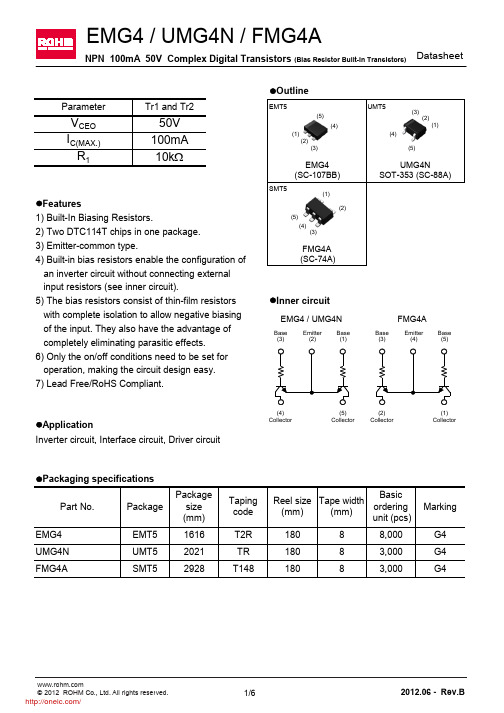
DatasheetEMG4 / UMG4N / FMG4ANPN 100mA 50V Complex Digital Transistors (Bias Resistor Built-in Transistors)l Outlinel Features1) Built-In Biasing Resistors.2) Two DTC114T chips in one package.3) Emitter-common type.4) Built-in bias resistors enable the configuration of an inverter circuit without connecting external input resistors (see inner circuit).5) The bias resistors consist of thin-film resistors l Inner circuitwith complete isolation to allow negative biasing of the input. They also have the advantage of completely eliminating parasitic effects.6) Only the on/off conditions need to be set for operation, making the circuit design easy.7) Lead Free/RoHS Compliant.l ApplicationInverter circuit, Interface circuit, Driver circuitl Packaging specifications3,000G4UMG4N UMT52021TR 1808SMT52928T14818088,000G48Tape width(mm)Basicorderingunit (pcs)Marking Reel size (mm)EMG4EMT51616T2R 1803,000G4FMG4APart No.Package Package size (mm)Taping code R 110k WParameterTr1 and Tr2V CEO 50V I C(MAX.)100mA EMT5UMT5SMT5EMG4 (SC-107BB)FMG4A (SC-74A)UMG4NSOT-353 (SC-88A)(1)(5) (4)(2)(3)Collector Base (3)Emitter (2)Collector Base (1)Collector Base (3)Emitter (4)CollectorBase (5)EMG4 / UMG4NFMG4A(5)(1) (2)(4)(3)(2)(1)(3)(4)(5)l Absolute maximum ratings (Ta = 25°C)l Electrical characteristics(Ta = 25°C)*2 Each terminal mounted on a reference footprint *3 120mW per element must not be exceeded.*4 200mW per element must not be exceeded.l Electrical characteristic curves(Ta = 25°C)COLLECTORCURRENT:Ic(mA)BASE TO EMITTER VOLTAGE : V BE (V) COLLECTOR TO EMITTERVOLTAGE : V CE (V)Fig.3 DC Current gainvs. Collector CurrentDCCURRENTGAIN:hFECOLLECTOR CURRENT : I C (mA)Fig.4 Collector-emitter saturation voltagevs. Collector CurrentCOLLECTORSATURATIONVOLTAGE:VCE(sat)(V)COLLECTOR CURRENT : I C (mA)05100.0010.010.111000.51 1.52Dimension in mm/inchesEMT5Patterm of terminal position areasDimension in mm/inchesUMT5Patterm of terminal position areasDimension in mm/inchesSMT5Patterm of terminal position areasNoticeN o t e sNo copying or reprod uction of this d ocument, in part or in whole, is permitted without theconsent of ROHM Co.,Ltd.The content specified herein is subject to change for improvement without notice.The content specified herein is for the purpose of introd ucing ROHM's prod ucts (hereinafter"Products"). If you wish to use any such Product, please be sure to refer to the specifications,which can be obtained from ROHM upon request.Examples of application circuits, circuit constants and any other information contained hereinillustrate the standard usage and operations of the Products. The peripheral conditions mustbe taken into account when designing circuits for mass production.Great care was taken in ensuring the accuracy of the information specified in this document.However, should you incur any d amage arising from any inaccuracy or misprint of suchinformation, ROHM shall bear no responsibility for such damage.The technical information specified herein is intended only to show the typical functions of andexamples of application circuits for the Prod ucts. ROHM d oes not grant you, explicitly orimplicitly, any license to use or exercise intellectual property or other rights held by ROHM andother parties. ROHM shall bear no responsibility whatsoever for any dispute arising from theuse of such technical information.The Products specified in this document are intended to be used with general-use electronicequipment or devices (such as audio visual equipment, office-automation equipment, commu-nication devices, electronic appliances and amusement devices).The Products specified in this document are not designed to be radiation tolerant.While ROHM always makes efforts to enhance the quality and reliability of its Prod ucts, aProduct may fail or malfunction for a variety of reasons.Please be sure to implement in your equipment using the Products safety measures to guardagainst the possibility of physical injury, fire or any other damage caused in the event of thefailure of any Product, such as derating, redundancy, fire control and fail-safe designs. ROHMshall bear no responsibility whatsoever for your use of any Product outside of the prescribedscope or not in accordance with the instruction manual.The Products are not designed or manufactured to be used with any equipment, device orsystem which requires an extremely high level of reliability the failure or malfunction of whichmay result in a direct threat to human life or create a risk of human injury (such as a medicalinstrument, transportation equipment, aerospace machinery, nuclear-reactor controller, fuel-controller or other safety device). ROHM shall bear no responsibility in any way for use of anyof the Prod ucts for the above special purposes. If a Prod uct is intend ed to be used for anysuch special purpose, please contact a ROHM sales representative before purchasing.If you intend to export or ship overseas any Product or technology specified herein that maybe controlled under the Foreign Exchange and the Foreign Trade Law, you will be required toobtain a license or permit under the Law.Thank you for your accessing to ROHM product informations.More detail product informations and catalogs are available, please contact us.ROHM Customer Support System/contact/分销商库存信息: ROHMEMG4T2R。
CM6400A;中文规格书,Datasheet资料

CM6400AEMI Filters with ESD Protection for Data Line ApplicationsProduct DescriptionThe CM6400A is a 24−bump EMI filter with ESD protection device for data line application in a 0.4 mm pitch, 5 x 5 CSP form factor. It is fully compliant with IEC 61000−4−2 Level 4. The CM6400A is RoHS II compliant.Features•24−Bump, 1.96 mm X 1.96 mm Footprint Chip Scale Package •These Devices are Pb −Free and are RoHS CompliantMARKING DIAGRAMDevice Package Shipping †ORDERING INFORMATIONCSP −24(Pb −Free)5000/T ape & ReelCM6400A64P3= CM6400A YYWW = Date CodeXXXX = Last four digits of lot#WLCSP24CASE 567CK†For information on tape and reel specifications,including part orientation and tape sizes, please refer to our Tape and Reel Packaging Specification Brochure, BRD8011/D.ELECTRICAL SCHEMATIC64P3YYWWXXXXRGND1 of 10 Filter Channels+LPACKAGE / PINOUT DIAGRAMSBottom View (Bumps Up View)Top View(Bumps Down View)A BC D EOrientation MarkingA1 Corner IndicatorTable 1. PIN DESCRIPTIONSA5 = Line 1A4 = Line 2A3 = GNDA2 = Line 1A1 = Line 2B5 = Line 3B4 = Line 4B2 = Line 3B1 = Line 4C5 = Line 5C4 = Line 6C3 = GND C2 = Line 5C1 = Line 6D5 = Line 7D4 = Line 8D3 = GND D2 = Line 7D1 = Line 8E5 = Line 9E4 = Line 10E3 = GND E2 = Line 9E1 = Line 10ELECTRICAL SPECIFICATIONS AND CONDITIONSTable 2. PARAMETERS AND OPERATING CONDITIONSParameterRating Units Storage Temperature Range –55 to +150°C Operating Temperature Range –40 to +85°C Power Dissipation at 70°C per Channel60mWTable 3. ELECTRICAL OPERATING CHARACTERISTICS (Note 1)Symbol ParameterConditionsMin Typ Max Units R Resistance 100125150W L Inductance(Note 2)35nH CCapacitance per ChannelAt 1 MHz, V IN = 0 V (Notes 2 and 3)192429pF At 1 MHz, V IN = 2.5 V15pF Att(5)Passband Attenuation at 5 MHz −7dB F C Cut −off Frequency Z SOURCE = 50 W , Z LOAD = 50 W 250MHz V BR Breakdown VoltageI R = ±1 mA ±6±7.8±10V I LEAK Leakage Current per ChannelV IN = 3.0 V 10100nA V ESDESD Peak Discharge Voltage Protection at All Pins:a) Contact Discharge per IEC 61000−4−2 standardb) Air Discharge per IEC 61000−4−2 standard(Notes 2, 3 and 4)±15±15kV1.All parameters specified at T A = 25°C unless otherwise noted.2.These parameters guaranteed by design.3.These parameters guaranteed by characterization.4.Standard IEC 61000−4−2 (C Discharge = 150 pF, R Discharge = 330 W ).RF CHARACTERISTICSFigure 1. Typical Insertion Loss (Bias = 0 V, T A = 255C, 50 W Environment)PACKAGE DIMENSIONSWLCSP24, 1.96x1.96CASE 567CK −01ISSUE ONOTES:1.DIMENSIONING AND TOLERANCING PER ASME Y14.5M, 1994.2.CONTROLLING DIMENSION: MILLIMETERS.3.COPLANARITY APPLIES TO SPHERICAL CROWNS OF SOLDER BALLS.2X DIM A MIN MAX0.57MILLIMETERS A1D 1.96 BSC E b 0.240.29e0.40 BSC0.630.170.241.96 BSC DIMENSIONS: MILLIMETERS*For additional information on our Pb −Free strategy and soldering details, please download the ON Semiconductor Soldering and Mounting Techniques Reference Manual, SOLDERRM/D.SOLDERING FOOTPRINT*BOTTOM VIEWA20.40 REF RECOMMENDEDON Semiconductor and are registered trademarks of Semiconductor Components Industries, LLC (SCILLC). SCILLC reserves the right to make changes without further notice to any products herein. SCILLC makes no warranty, representation or guarantee regarding the suitability of its products for any particular purpose, nor does SCILLC assume any liability arising out of the application or use of any product or circuit, and specifically disclaims any and all liability, including without limitation special, consequential or incidental damages.“Typical” parameters which may be provided in SCILLC data sheets and/or specifications can and do vary in different applications and actual performance may vary over time. All operating parameters, including “Typicals” must be validated for each customer application by customer’s technical experts. SCILLC does not convey any license under its patent rights nor the rights of others. SCILLC products are not designed, intended, or authorized for use as components in systems intended for surgical implant into the body, or other applications intended to support or sustain life, or for any other application in which the failure of the SCILLC product could create a situation where personal injury or death may occur. Should Buyer purchase or use SCILLC products for any such unintended or unauthorized application, Buyer shall indemnify and hold SCILLC and its officers, employees, subsidiaries, affiliates,and distributors harmless against all claims, costs, damages, and expenses, and reasonable attorney fees arising out of, directly or indirectly, any claim of personal injury or death associated with such unintended or unauthorized use, even if such claim alleges that SCILLC was negligent regarding the design or manufacture of the part. SCILLC is an Equal Opportunity/Affirmative Action Employer. This literature is subject to all applicable copyright laws and is not for resale in any manner.PUBLICATION ORDERING INFORMATION分销商库存信息: ONSEMICM6400A。
192R,AL,192R,BK,192R,GY, 规格书,Datasheet 资料
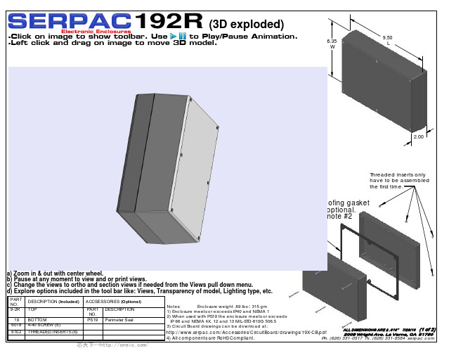
192R (3D exploded)
6.35 W
9.50 L
2.00
Threaded inserts only have to be assembled the first time.
Notes: Enclosure weight .69 lbs / 315 gm 1) Enclosure meets or exceeds IP40 and NEMA 1 2) When used with PS19 the enclosure meets or exceeds IP 66 and NEMA 4X, 12 and 13 MIL-STD-810G 506.5 3) Circuit Board drawings can be download at: ALL DIMENSIONS ARE ± .010" 7/29/10 (1 of 2) /Accessories/CircuitBoard/drawings/19X-CB.pdf 2009 Wright Ave. La Verne, CA 91750 4) All components are RoHS Compliant. Ph. (626) 331-0517 Fx. (626) 331-8584
芯天下--/
Notes: Enclosure weight .69 lbs / 315 gm .32 1) Enclosure meets or exceeds IP40 and NEMA 1 6 plc's SECTION A-A 2) When used with PS19 the enclosure meets or exceeds SCALE 1 : 2.75 IP 67 and NEMA 4X, 12 and 13 MIL-STD-810G 506.5 3) Circuit Board drawings can be download at: ALL DIMENSIONS ARE ± .010" 7/29/10 (2 of 2) /Accessories/CircuitBoard/drawings/19X_CB.pdf 2009 Wright Ave. La Verne, CA 91750 4) All components are RoHS Compliant. Ph. (626) 331-0517 Fx. (626) 331-8584
4840N;中文规格书,Datasheet资料
/
分销商库存信息:
EBM-PAPST 4840N
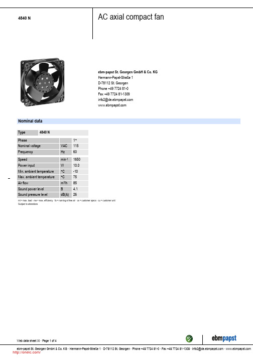
ml = max. load · me = max. efficiency · fa = running at free air · cs = customer specs · cu = customer unit Subject to alterations
Web data sheet XI · Page 1 of 4 ebm-papst St. Georgen GmbH & Co. KG · Hermann-Papst-Straße 1 · D-78112 St. Georgen · Phone +49 7724 81-0 · Fax +49 7724 81-1309 · info2@ ·
/
4840 N
AC axial compact fan
Product drawing
Web data sheet XI · Page 3 of 4 ebm-papst St. Georgen GmbH & Co. KG · Hermann-Papst-Straße 1 · D-78112 St. Georgen · Phone +49 7724 81-0 · Fax +49 7724 81-1309 · info2@ ·
Mass Dimensions Material of impeller Housing material Direction of air flow Direction of rotation Bearing Lifetime L10 at 40 °C Lifetime L10 at maximum temperature Connection line Motor protection Approval
APT24F50B;中文规格书,Datasheet资料

25 TJ = -55°C
TJ = 25°C 20
TJ = 125°C
15
10
5
0
0
5
10
15
20
25
ID, DRAIN CURRENT (A) Figure 5, Gain vs Drain Current
4 Co(cr) is defined as a fixed capacitance with the same stored charge as COSS with VDS = 67% of V(BR)DSS. 5 Co(er) is defined as a fixed capacitance with the same stored energy as COSS with VDS = 67% of V(BR)DSS. To calculate Co(er) for any value of
VGS = 0V, VDS = 0V to 333V
Qg Qgs Qgd td(on)
tr td(off)
tf
Total Gate Charge Gate-Source Charge Gate-Drain Charge Turn-On Delay Time Current Rise Time Turn-Off Delay Time Current Fall Time
nC ns
Source-Drain Diode Characteristics
Symbol Parameter
Test Conditions
Min Typ Max Unit
IS ISM VSD trr Qrr Irrm
dv/dt
Continuous Source Current (Body Diode) Pulsed Source Current (Body Diode) 1 Diode Forward Voltage Reverse Recovery Time
XH4A-6031-A;中文规格书,Datasheet资料
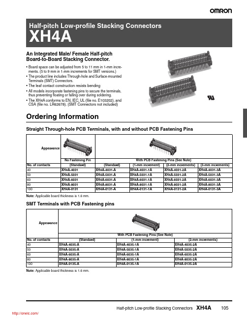
Half-pitch Low-profile Stacking Connectors XH4A105An Integrated Male/ Female Half-pitch Board-to-Board Stacking Connector.•Board space can be adjusted from 5 to 11 mm in 1-mm incre-ments. (5 to 9 mm in 1-mm increments for SMT versions.)•The product line includes Through-hole and Surface-mounted Terminals (SMT) Connectors.•The leaf contact construction resists bending•All models incorporate fastening pins to secure the terminals, thus preventing floating or falling over during soldering.•The XH4A conforms to EN, IEC, UL (file no. E103202), andCSA (file no. LR62678). (SMT Connectors not included)Ordering InformationStraight Through-hole PCB Terminals, with and without PCB Fastening PinsNote:Applicable board thickness is 1.6 mm.SMT Terminals with PCB Fastening pinsNote:Applicable board thickness is 1.6 mm.AppearanceNo Fastening PinWith PCB Fastening Pins (See Note)No. of contacts (Standard)(Standard)(1-mm increment)(2-mm increments)(3-mm increments)40XH4A-4031XH4A-4031-A XH4A-4031-1A XH4A-4031-2A XH4A-4031-3A 50XH4A-5031XH4A-5031-A XH4A-5031-1A XH4A-5031-2A XH4A-5031-3A 60XH4A-6031XH4A-6031-A XH4A-6031-1A XH4A-6031-2A XH4A-6031-3A 80XH4A-8031XH4A-8031-A XH4A-8031-1A XH4A-8031-2A XH4A-8031-3A 100XH4A-0131XH4A-0131-AXH4A-0131-1AXH4A-0131-2AXH4A-0131-3AAppearanceWith PCB Fastening Pins (See Note)No. of contacts (Standard)(1-mm increment)(2-mm increments)40XH4A-4035-A XH4A-4035-1A XH4A-4035-2A 50XH4A-5035-A XH4A-5035-1A XH4A-5035-2A 60XH4A-6035-A XH4A-6035-1A XH4A-6035-2A 80XH4A-8035-A XH4A-8035-1A XH4A-8035-2A 100XH4A-0135-AXH4A-0135-1AXH4A-0135-2A106Half-pitch Low-profile Stacking Connectors XH4ASpecifications■Ratings and CharacteristicsNote:The contact resistance depends on which XH4A-@@31 Connectors are mated to each other.■Materials and FinishEngineering Data■Mating DiagramsStacked Through-hole DIP TerminalsStacked SMT TerminalsRated current 0.5 A Rated voltage125 VACContact resistance (See note.)30 m Ω max. (20 mV max., 100 mA max.)Insulation resistance 1,000 M Ω min. (at 500 VDC)Dielectric strength 650 VAC for 1 min (leakage current: 1 mA max.)Connector insertion force 150 gf (1.47 N) max. per contact Connector removal force 15 gf (0.15 N) min. per contact Insertion tolerance 50 timesAmbient temperatureOperating: −55 to 105°C (with no icing)Housing PPS resin with glass (UL94V-0)/black Locator PBT resin with glass (UL94V-0)/blackContactsMating end Phosphor bronze/nickel base, 0.15-μm gold plating TerminalPhosphor bronze/nickel base, gold flash plating Fastening pinsPhosphor bronze/tin platingStacking space 5 mm 6 mm 7 mm8 mmMating diagramStacking space 9 mm10 mm11 mmMating diagramXH4A-@@31(-A)XH4A-@@31(-A)XH4A-@@31(-A)XH4A-@@31-1A XH4A-@@31-1AXH4A-@@31-1A XH4A-@@31-1AXH4A-@@31-2AXH4A-@@31-2AXH4A-@@31-2AXH4A-@@31-2AXH4A-@@31-3A XH4A-@@31-3AXH4A-@@31-3AStacking space 5 mm6 mm7 mm8 mm9 mmMating diagramHalf-pitch Low-profile Stacking Connectors XH4A107■Contact NumbersNote:1.The triangular mark (▼) and contact numbers are not printed on the connectors. Use the raised reference point used to prevent reverseinsertion as a guide when designing boards.2.On the mating side, the row of terminals on the raised reference point side are called row a, and the row on the other side is called row b. The numbers are in the order shown.3.XH4A Half-pitch Connectors are integrated male/female connectors. The contact numbers on row a correspond to the contact numbers on row b. Be careful when using these connectors because they function slightly differently from separate male and female connectors (i.e., Plugs and Sockets).Dimensions■Straight Through-hole DIP Terminals (without PCB fastening pins)Item Model Mated DiagramMounting holesThrough-hole Terminals(bottom view)SMT T erminals (top view)ReferenceReferenceReference ReferenceReferenceMountin g holes (b ottom v ie w )Reference0.8 dia.+0.10T w o, 1.1 dia.+0.1XH4A-@@31No. of contacts Dimensions (mm)A B C 4032.7324.1328.635039.0830.4834.986045.4336.8341.338058.1349.5354.0310070.8362.2366.73108Half-pitch Low-profile Stacking Connectors XH4A■XH4A Straight Through-hole Terminals (with PCB fastening pins)Stacking Space Adjustable in Standard Size and 1-, 2-, or 3-mm Increments■XH4A SMT Terminals (with PCB fastening pins)Stacking Space Adjustable in Standard Size and 1- or 2-mm IncrementsReferenceMountin gholes (b ottom v ie w )Reference3-mm increments2-mm increments1-mm incrementsStandard0.8 dia.+0.1T w o, 2.8 dia.+0.1XH4A-@@31-A (Standard)XH4A-@@31-1A (1-mm Increment)XH4A-@@31-2A (2-mm Increments)XH4A-@@31-3A (3-mm Increments)No. of contacts Dimensions (mm)A B C 4032.7324.1330.235039.0830.4836.586045.4336.8342.938058.1349.5355.6310070.8362.2368.33Mountin g holes (top v ie w )Ro w A2-mm increments1-mm incrementsStandardRo w B Ro w ARo w BRo w ARo w BReferenceT w o, 2.8 dia.+0.11 dia.DXH4A-@@35-A (Standard)XH4A-@@35-1A (1-mm Increment)XH4A-@@35-2A (2-mm Increments)No. of contacts Dimensions (mm)A B C 4032.7324.1330.235039.0830.4836.586045.4336.8342.938058.1349.5355.6310070.8362.2368.33Half-pitch Low-profile Stacking Connectors XH4A109Precautions■Correct UsePCB settingsXH4A Half-pitch Connectors are male/female connectors with inte-grated plugs and sockets.Refer to “Contact Numbers” in the “Engineering Data ” section above when designing boards.Mating CompatibilityXH4 Half-pitch Connectors do not mate with XH2 or XH3 Half-pitch Connectors.Soldering ConditionsStraight DIP Terminals (Automated Soldering)1.Soldering temperature: 230±5°C2.Continuous soldering time: Within 3 sBe sure to wash the board after automated soldering is completed.SMT Terminals 1.Recommended reflow conditions:2.Pre-heat temperature: 150±10°C 3.Pre-heat time: 60 to 120s4.Soldering temperature: 200 to 240°C5.Soldering time: Within 30s (Within 10s at the maximum temperature of 240°C)Half-pitch Low-profile Stacking Connectors XH4AOMRON ON-LINEGlobal - USA - Cat. No. X304-E-1Printed in USAOMRON ELECTRONIC COMPONENTS LLC55 E. Commerce Drive, Suite B Schaumburg, IL 60173847-882-228811/10 Specifications subject to change without noticeAll sales are subject to Omron Electronic Components LLC standard terms and conditions of sale, which can be found at /components/web/webfiles.nsf/sales_terms.html ALL DIMENSIONS SHOWN ARE IN MILLIMETERS.T o convert millimeters into inches, multiply by 0.03937. T o convert grams into ounces, multiply by 0.03527.分销商库存信息: OMRONXH4A-6031-A。
MBRA140T3G;MBRA140T3;中文规格书,Datasheet资料
Figure 5. Current Derating
R (T) , TRANSIENT THERMAL RESISTANCE (NORMALIZED) T, TIME (s) 1.0E+0
Figure 6. Forward Power Dissipation
中文规格书datasheet资料datasheetdatasheet网站l298ndatasheeticdatasheetpl2303datasheetds18b20datasheetdatasheetcomlm324datasheetrt5350datasheet
MBRA140T3G, NRVBA140T3G Surface Mount Schottky Power Rectifier
vF, INSTANTANEOUS FORWARD VOLTAGE (VOLTS)
Figure 1. Typical Forward Voltage
Figure 2. Maximum Forward Voltage
100E-3 I R , REVERSE CURRENT (AMPS)
100E-3 I R , MAXIMUM REVERSE CURRENT (AMPS)
†For information on tape and reel specifications, including part orientation and tape sizes, please refer to our Tape and Reel Packaging Specifications Brochure, BRD8011/D.
10E-3
TJ = 125C TJ = 85C
10E-3 TJ = 85C 1.0E-3 TJ = 25C
24AA014H-ISN;24LC014H-IMS;24LC014HT-IMNY;24AA014HT-IMNY;24AA014H-IP;中文规格书,Datasheet资料
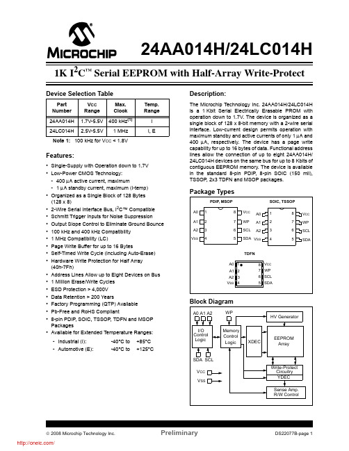
24AA014H/24LC014HDevice Selection TableFeatures:•Single-Supply with Operation down to 1.7V •Low-Power CMOS Technology:-400 μA active current, maximum- 1 μA standby current, maximum (I-temp)•Organized as a Single Block of 128 Bytes(128 x 8)•2-Wire Serial Interface Bus, I2C™ Compatible •Schmitt Trigger Inputs for Noise Suppression •Output Slope Control to Eliminate Ground Bounce •100 kHz and 400 kHz Compatibility• 1 MHz Compatibility (LC)•Page Write Buffer for up to 16 Bytes•Self-Timed Write Cycle (including Auto-Erase)•Hardware Write Protection for Half Array(40h-7Fh)•Address Lines Allow up to Eight Devices on Bus • 1 Million Erase/Write Cycles•ESD Protection > 4,000V•Data Retention > 200 Years•Factory Programming (QTP) Available•Pb-Free and RoHS Compliant•8-pin PDIP, SOIC, TSSOP, TDFN and MSOP Packages•Available for Extended Temperature Ranges:Description:The Microchip Technology Inc. 24AA014H/24LC014H is a 1Kbit Serial Electrically Erasable PROM with operation down to 1.7V. The device is organized as a single block of 128 x8-bit memory with a 2-wire serial interface. Low-current design permits operation with maximum standby and active currents of only 1 μA and 400 μA, respectively. The device has a page write capability for up to 16 bytes of data. Functional address lines allow the connection of up to eight 24AA014H/ 24LC014H devices on the same bus for up to 8Kbits of contiguous EEPROM memory. The device is available in the standard 8-pin PDIP, 8-pin SOIC (150 mil), TSSOP, 2x3 TDFN and MSOP packages. Package TypesBlock DiagramPart NumberV CCRangeMax.ClockTemp.Range24AA014H 1.7V-5.5V400kHz(1)I 24LC014H 2.5V-5.5V 1 MHz I, E Note1:100 kHz for V CC < 1.8V-Industrial (I):-40°C to+85°C -Automotive (E):-40°C to+125°CA0A1A2V SSV CCWPSCLSDA12348765PDIP, MSOP SOIC, TSSOPA0A1A2V SS12348765V CCWPSCLSDATDFNA0A1A2V SSWPSCLSDAV CC87651234I/OControlLogicMemoryControlLogic XDECHV GeneratorEEPROMArrayWrite-ProtectCircuitryYDEC V CCV SSSense Amp.R/W ControlSDA SCLA0 A1 A2WP1K I2C™ Serial EEPROM with Half-Array Write-Protect© 2008 Microchip Technology Inc.Preliminary DS22077B-page 124AA014H/24LC014HDS22077B-page 2Preliminary© 2008 Microchip Technology Inc.1.0ELECTRICAL CHARACTERISTICSAbsolute Maximum Ratings (†)V CC .............................................................................................................................................................................6.5V All inputs and outputs w.r.t. V SS .........................................................................................................-0.6V to V CC +1.0V Storage temperature ...............................................................................................................................-65°C to +150°C Ambient temperature with power applied................................................................................................-40°C to +125°C ESD protection on all pins ......................................................................................................................................................≥ 4 kV † NOTICE : Stresses above those listed under “Absolute Maximum Ratings” may cause permanent damage to the device. This is a stress rating only and functional operation of the device at those or any other conditions above those indicated in the operational listings of this specification is not implied. Exposure to maximum rating conditions for extended periods may affect device reliability.TABLE 1-1:DC CHARACTERISTICSAll parameters apply across the specified operating ranges unless otherwise noted.Electrical Characteristics:Industrial (I):V CC = +1.7V to 5.5V T A = -40°C to +85°C Automotive (E):V CC = +2.5V to 5.5V T A = -40°C to +125°CParameterSymbol Min.Max.Units ConditionsSCL and SDA pins:High-level input voltage V IH 0.7 V CC—V Low-level input voltageV IL —0.3 V CCV Hysteresis of Schmitt Trigger inputs V HYS 0.05 V CC—V (Note 1)Low-level output voltage V OL —0.40V I OL = 3.0 mA, V CC = 4.5V I OL = 2.1 mA, V CC = 2.5V Input leakage current I LI —±1μΑV IN = V SS or V CC , WP = Vss Output leakage currentI LO —±1μA V OUT = V SS or V CC Pin capacitance (all inputs/outputs)C IN , C OUT —10pF V CC = 5.0V (Note 1)T A = 25°C, f = 1 MHz Operating current I CC Read —400μA V CC = 5.5V, SCL = 400 kHz I CC Write —3mA V CC = 5.5VStandby currentI CCS—1μAV CC = 5.5V, SDA = SCL = V CC WP = V SS , A0, A1, A2 = V SS Note 1:This parameter is periodically sampled and not 100% tested.24AA014H/24LC014H TABLE 1-2:AC CHARACTERISTICSAC CHARACTERISTICS Electrical Characteristics:Industrial (I):V CC = +1.7V to 5.5V T A = -40°C to +85°C Automotive (E):V CC = +2.5V to 5.5V T A = -40°C to +125°CParam.No.Symbol Characteristic Min.Max.Units Conditions1F CLK Clock frequency———1004001000kHz 1.7V ≤ V CC < 1.8V1.8V ≤ V CC≤ 5.5V2.5V ≤ V CC≤ 5.5V (24LC014H)2T HIGH Clock high time4000600500———ns 1.7V ≤ V CC < 1.8V1.8V ≤ V CC≤ 5.5V2.5V ≤ V CC≤ 5.5V (24LC014H)3T LOW Clock low time47001300500———ns 1.7V ≤ V CC < 1.8V1.8V ≤ V CC≤ 5.5V2.5V ≤ V CC≤ 5.5V (24LC014H)4T R SDA and SCL rise time (Note1)———1000300300ns 1.7V ≤ V CC < 1.8V1.8V ≤ V CC≤ 5.5V2.5V ≤ V CC≤ 5.5V (24LC014H)5T F SDA and SCL fall time (Note1)———1000300300ns 1.7V ≤ V CC < 1.8V1.8V ≤ V CC≤ 5.5V2.5V ≤ V CC≤ 5.5V (24LC014H)6T HD:STA Start condition hold time4000600250———ns 1.7V ≤ V CC < 1.8V1.8V ≤ V CC≤ 5.5V2.5V ≤ V CC≤ 5.5V (24LC014H)7T SU:STA Start condition setup time4700600250———ns 1.7V ≤ V CC < 1.8V1.8V ≤ V CC≤ 5.5V2.5V ≤ V CC≤ 5.5V (24LC014H)8T HD:DAT Data input hold time0—ns(Note2)9T SU:DAT Data input setup time250100100———ns 1.7V ≤ V CC < 1.8V1.8V ≤ V CC≤ 5.5V2.5V ≤ V CC≤ 5.5V (24LC014H)10T SU:STO Stop condition setup time4000600250———ns 1.7V ≤ V CC < 1.8V1.8V ≤ V CC≤ 5.5V2.5V ≤ V CC≤ 5.5V (24LC014H)11T SU:WP WP setup time4000600600———ns 1.7V ≤ V CC < 1.8V1.8V ≤ V CC≤ 5.5V2.5V ≤ V CC≤ 5.5V (24LC014H)12T HD:WP WP hold time4700600600———ns 1.7V ≤ V CC < 1.8V1.8V ≤ V CC≤ 5.5V2.5V ≤ V CC≤ 5.5V (24LC014H)13T AA Output valid from clock (Note2)———3500900400ns 1.7V ≤ V CC < 1.8V1.8V ≤ V CC≤ 5.5V2.5V ≤ V CC≤ 5.5V (24LC014H)14T BUF Bus free time: Time the bus mustbe free before a new transmissioncan start 130047004700———ns 1.7V ≤ V CC < 1.8V1.8V ≤ V CC≤ 5.5V2.5V ≤ V CC≤ 5.5V (24LC014H)16T SP Input filter spike suppression(SDA and SCL pins)—50ns24AA014H(Note1 and Note3)17T WC Write cycle time (byte or page)—5ms—18—Endurance1M—cycles25°C, V CC = 5.5V, Block mode(Note4)Note1:Not 100% tested. C B = total capacitance of one bus line in pF.2:As a transmitter, the device must provide an internal minimum delay time to bridge the undefined region (minimum 300ns) of the falling edge of SCL to avoid unintended generation of Start or Stop conditions.3:The combined T SP and V HYS specifications are due to new Schmitt Trigger inputs, which provide improved noise spike suppression. This eliminates the need for a T I specification for standard operation.4:This parameter is not tested but ensured by characterization. For endurance estimates in a specific application, please consult the Total Endurance™ Model which can be obtained from Microchip’s web site at .© 2008 Microchip Technology Inc.Preliminary DS22077B-page 324AA014H/24LC014HDS22077B-page 4Preliminary© 2008 Microchip Technology Inc.FIGURE 1-1:BUS TIMING DATA(unprotected)(protected)SCL SDA InSDA OutWP 57616328913D441011121424AA014H/24LC014H2.0PIN DESCRIPTIONSThe descriptions of the pins are listed in Table2-1.TABLE 2-1:PIN FUNCTION TABLE2.1SDA Serial DataThis is a bidirectional pin used to transfer addresses and data into and out of the device. It is an open drain terminal. Therefore, the SDA bus requires a pull-up resistor to V CC (typical 10 kΩ for 100 kHz, 2 kΩ for 400kHz).For normal data transfer SDA is allowed to change only during SCL low. Changes during SCL high are reserved for indicating the Start and Stop conditions.2.2SCL Serial ClockThe SCL input is used to synchronize the data transfer to and from the device.2.3A0, A1, A2The A0, A1 and A2 inputs are used by the 24AA014H/ 24LC014H for multiple device operations. The levels on these inputs are compared with the corresponding bits in the slave address. The chip is selected if the compare is true.Up to eight 24AA014H/24LC014H devices may be connected to the same bus by using different Chip Select bit combinations. These inputs must be connected to either V CC or V SS.In most applications, the chip address inputs A0, A1 and A2 are hard-wired to logic ‘0’ or logic ‘1’. For applications in which these pins are controlled by a microcontroller or other programmable device, the chip address pins must be driven to logic ‘0’ or logic ‘1’before normal device operation can proceed.2.4WPWP is the hardware write-protect pin. It must be tied to V CC or V SS. If tied to V CC, the hardware write protection is enabled and will protect half of the array (40h-7Fh). If the WP pin is tied to V SS the hardware write protection is disabled.2.5Noise ProtectionThe 24AA014H/24LC014H employs a V CC threshold detector circuit that disables the internal erase/write logic if the V CC is below 1.5 volts at nominal conditions. The SCL and SDA inputs have Schmitt Trigger and filter circuits that suppress noise spikes to assure proper device operation even on a noisy bus.Name 8-pinPDIP8-pinSOIC8-pinTSSOP8-pinMSOP8-pinTDFNFunctionA011111User Configurable Chip SelectA122222User Configurable Chip SelectA233333User Configurable Chip SelectV SS44444GroundSDA55555Serial DataSCL66666Serial ClockWP77777Write-Protect InputV CC88888+1.7V to 5.5V (24AA014H)+2.5V to 5.5V (24LC014H)© 2008 Microchip Technology Inc.Preliminary DS22077B-page 524AA014H/24LC014HDS22077B-page 6Preliminary© 2008 Microchip Technology Inc.3.0FUNCTIONAL DESCRIPTIONThe 24AA014H/24LC014H supports a bidirectional,2-wire bus and data transmission protocol. A device that sends data onto the bus is defined as transmitter,and a device receiving data as receiver. The bus has to be controlled by a master device that generates the Serial Clock (SCL), controls the bus access and gen-erates the Start and Stop conditions while the 24AA014H/24LC014H works as slave. Both master and slave can operate as transmitter or receiver, but the master device determines which mode is activated.4.0BUS CHARACTERISTICSThe following bus protocol has been defined:•Data transfer may be initiated only when the bus is not busy.•During data transfer, the data line must remain stable whenever the clock line is high. Changes in the data line while the clock line is high will be interpreted as a Start or Stop condition.Accordingly, the following bus conditions have been defined (Figure 4-1).4.1Bus Not Busy (A)Both data and clock lines remain high.4.2Start Data Transfer (B)A high-to-low transition of the SDA line while the clock (SCL) is high determines a Start condition. All commands must be preceded by a Start condition.4.3Stop Data Transfer (C)A low-to-high transition of the SDA line while the clock (SCL) is high determines a Stop condition. All operations must be ended with a Stop condition.4.4Data Valid (D)The state of the data line represents valid data when,after a Start condition, the data line is stable for the duration of the high period of the clock signal.The data on the line must be changed during the low period of the clock signal. There is one bit of data per clock pulse.Each data transfer is initiated with a Start condition and terminated with a Stop condition. The number of the data bytes transferred between the Start and Stop conditions is determined by the master device and is,theoretically, unlimited, though only the last sixteen will be stored when doing a write operation. When an overwrite does occur, it will replace data in a first-in first-out fashion.4.5AcknowledgeEach receiving device, when addressed, is required to generate an acknowledge after the reception of each byte. The master device must generate an extra clock pulse which is associated with this Acknowledge bit.The device that acknowledges has to pull down the SDA line during the Acknowledge clock pulse in such a way that the SDA line is stable low during the high period of the acknowledge-related clock pulse. Of course, setup and hold times must be taken into account. A master must signal an end of data to the slave by not generating an Acknowledge bit on the last byte that has been clocked out of the slave. In this case,the slave must leave the data line high to enable the master to generate the Stop condition (Figure 4-2).Note:The 24AA014H/24LC014H does not gen-erate any Acknowledge bits if an internal programming cycle is in progress.24AA014H/24LC014H© 2008 Microchip Technology Inc.Preliminary DS22077B-page 724AA014H/24LC014HDS22077B-page 8Preliminary© 2008 Microchip Technology Inc.5.0DEVICE ADDRESSINGA control byte is the first byte received following the Start condition from the master device (Figure 5-1).The control byte consists of a four-bit control code; for the 24AA014H/24LC014H this is set as ‘1010’ binary for read and write operations. The next three bits of the control byte are the Chip Select bits (A2, A1, A0). The Chip Select bits allow the use of up to eight 24AA014H/24LC014H devices on the same bus and are used to select which device is accessed. The Chip Select bits in the control byte must correspond to the logic levels on the corresponding A2, A1 and A0 pins for the device to respond. These bits are in effect the three Most Significant bits of the word address.The last bit of the control byte defines the operation to be performed. When set to a ‘1’, a read operation is selected. When set to a ‘0’, a write operation is selected. Following the Start condition, the 24AA014H/24LC014H monitors the SDA bus, checking the control byte being transmitted. Upon receiving a ‘1010’ code and appropriate Chip Select bits, the slave device outputs an Acknowledge signal on the SDA line.24LC014H will select a read or write operation.FIGURE 5-1:CONTROL BYTE FORMAT5.1Contiguous Addressing Across Multiple DevicesThe Chip Select bits A2, A1 and A0 can be used to expand the contiguous address space for up to 8K bits by adding up to eight 24AA014H/24LC014H devices on the same bus. In this case, software can use A0 of the control byte as address bit A8, A1 as address bit A9,and A2 as address bit A10. It is not possible to sequentially read across device boundaries.11A2A1A0SACKR/W Control CodeChip SelectBits Slave AddressAcknowledge BitStart BitRead/Write Bit© 2008 Microchip Technology Inc.PreliminaryDS22077B-page 924AA014H/24LC014H6.0WRITE OPERATIONS6.1Byte WriteFollowing the Start signal from the master, the device code(4 bits), the Chip Select bits (3 bits) and the R/W bit (which is a logic low) are placed onto the bus by the master transmitter. The device will acknowledge this control byte during the ninth clock pulse. The next byte transmitted by the master is the word address and will be written into the Address Pointer of the 24AA014H/24LC014H. After receiving another Acknowledge signal from the 24AA014H/24LC014H, the master device will transmit the data word to be written into the addressed memory location. The 24AA014H/24LC014H acknowledges again and the master generates a Stop condition. This initiates the internal write cycle and the 24AA014H/24LC014H will not generate Acknowledge signals during this time (Figure 6-1). If an attempt is made to write to the protected portion of the array when the hardware write protection has been enabled, the device will acknowledge the command, but no data will be written.The write cycle time must be observed even if write protection is enabled.6.2Page WriteThe write-control byte, word address and the first data byte are transmitted to the 24AA014H/24LC014H in the same way as in a byte write. But instead of generating a Stop condition, the master transmits up to 15additional data bytes to the 24AA014H/24LC014H that are temporarily stored in the on-chip page buffer and will be written into the memory once the master has transmitted a Stop condition. Upon receipt of each word, the four lower order Address Pointer bits are internally incremented by one.The higher order four bits of the word address remain constant. If the master should transmit more than 16bytes prior to generating the Stop condition, the address counter will roll over and the previously received data will be overwritten. As with the byte write operation, once the Stop condition is received, an internal write cycle will begin (Figure 6-2). If an attempt is made to write to the protected portion of the array when the hardware write protection has been enabled,the device will acknowledge the command, but no data will be written. The write cycle time must be observed even if write protection is enabled.6.3Write ProtectionThe WP pin must be tied to V CC or V SS . If tied to V CC ,half of the array will be write-protected (40h-7Fh). If the WP pin is tied to V SS , write operations to all address locations are allowed.FIGURE 6-1:BYTE WRITEFIGURE 6-2:PAGE WRITENote:Page write operations are limited to writing bytes within a single physical page,regardless of the number of bytes actually being written. Physical page boundaries start at addresses that are integer multiples of the page buffer size (or ‘page size’) and end at addresses that are integer multiples of [page size – 1]. If a Page Write command attempts to write across a physical page boundary, the result is that the data wraps around to the beginning of the current page (overwriting data previously stored there), instead of being written to the next page, as might be expected. It is therefore necessary that the application software prevent page write operations that would attempt to cross a page boundary.SPBus Activity Master SDA Line Bus ActivityS T A R T S T O P Control ByteWord AddressDataA C KA C KA C KSPBus Activity Master SDA Line Bus ActivityS T A R T Control ByteWord Address (n)Data (n)Data (n + 15)S T O P A C KA C KA C KA C KA C KData (n +1)24AA014H/24LC014HDS22077B-page 10Preliminary© 2008 Microchip Technology Inc.7.0ACKNOWLEDGE POLLINGSince the device will not acknowledge during a write cycle, this can be used to determine when the cycle is complete (this feature can be used to maximize bus throughput). Once the Stop condition for a write command has been issued from the master, the device initiates the internally-timed write cycle and ACK polling can be initiated immediately. This involves the master sending a Start condition followed by the control byte for a Write command (R/W = 0). If the device is still busy with the write cycle, no ACK will be returned. If no ACK is returned, the Start bit and control byte must be re-sent. If the cycle is complete, the device will return the ACK and the master can then proceed with the next Read or Write command. See Figure 7-1 for a flow diagram of this operation.FIGURE 7-1:ACKNOWLEDGE POLLING FLOWSendWrite CommandSend Stop Condition to Initiate Write CycleSend StartSend Control Byte with R/W = 0Did Device Acknowledge (ACK = 0)?Next OperationNoYes分销商库存信息:MICROCHIP24AA014H-I/SN24LC014H-I/MS24LC014HT-I/MNY 24AA014HT-I/MNY24AA014H-I/P24AA014HT-I/SN 24LC014HT-I/SN24AA014H-I/MS24LC014H-I/ST24AA014H-I/ST24AA014HT-I/MS24AA014HT-I/ST 24LC014HT-I/MS24LC014HT-I/ST24LC014H-E/SN24LC014HT-E/SN24LC014H-E/MS24LC014H-E/ST24LC014HT-E/ST24LC014HT-E/MS24LC014HT-E/MNY 24LC014H-E/P24LC014H-I/SN24LC014H-I/P。
