M54HC02K中文资料
LM26CIM5-HHD中文资料
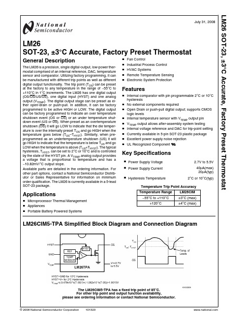
Analog output voltage proportional to temperature
Leave floating or connect to a high impedance node.
Supply input
2.7V to 5.5V with a 0.1µF bypass capacitor. For PSRR information see Section Titled NOISE CONSIDERATIONS.
Undertemperature Shutdown open-drain active System or power supply shutdown; pull-up resistor ≥ 10kΩ
low thermostat digital output
Undertemperature Shutdown push-pull active System or power supply shutdown high thermostat digital output
Overtemperature Shutdown open-drain active Controller interrupt, system or power supply shutdown; pull-up
low thermostat digital output
resistor ≥ 10kΩ
Overtemperature Shutdown push-pull active Controller interrupt, system or power supply shutdown high thermostat digital output
Available parts are detailed in the ordering information. For other part options, contact a National Semiconductor Distributor or Sales Representative for information on minimum order qualification. The LM26 is currently available in a 5-lead SOT-23 package.
M54HC1520C1R中文资料

M54/M74HC4518M54/M74HC4520March 1993HC4520DUAL 4BIT BINARY COUNTERHC4518DUAL DECADE COUNTER B1R(Plastic Package)ORDER CODES :M54HCXXXXF1R M74HCXXXXM1R M74HCXXXXB1R M74HCXXXXC1RF1R(Ceramic Package)M1R(Micro Package)C1R (Chip Carrier)PIN CONNECTIONS (top view)NC =No Internal Connecti o nDESCRIPTION.HIGH SPEEDf MAX =55MHz (TYP.)at V CC =5V .LOW POWER DISSIPATION I CC =4µA (MAX.)AT T A =25°C .HIGH NOISE IMMUNITYV NIH =V NIL =28%V CC (MIN.).OUTPUT DRIVE CAPABILITY 10LSTTL LOADS.SYMMETRICAL OUTPUT IMPEDANCE |I OH |=I OL =4mA (MIN.).BALANCED PROPAGATION DELAYS t PLH =t PHL.WIDE OPERATING VOLTAGE RANGE V CC (OPR)=2V TO 6V.PIN AND FUNCTION COMPATIBLE WITH 4520B/4518BThe M54/74HC4518/4520are high speed CMOS DUAL 4BIT BINARY COUNTERS fabricated in sili-con gate C 2MOS technology.They have the same high speed performance of LSTTL combined with true CMOS low power consumption.They consists of two identical internally syn-chronous 4-stage counters.The counter stages are D-type flip-flops having interchangeable Clock and ENABLE inputs for incrementing on either the posi-tive-going or negative-going transition.For single-unit operation the ENABLE input is main-tained ”high”and the counter advances on each positive-going transition of the CLOCK.The counters are cleared by high levels on their clear lines.The counter can be cascaded in the ripple mode by connecting Q4to the enable input of the subsequent counter while the clock input of the latter is held permanently low.All inputs are equipp ed with protection circuits against static discharge and transient excess volt-age.1/13M54/M74HC4518/4520 LOGIC DIAGRAM(1/2HC4518)LOGIC DIAGRAM(1/2HC4520) 2/13M54/M74HC4518/4520 TIMING CHART(HC4518)TIMING CHART(HC4520)3/13TRUTH TABLEINPUTSFUNCTION CLOCK ENABLE CLEARH L INCREMENT COUNTERL L INCREMENT COUNTERX L NO CHANGE X L NO CHANGEL L NO CHANGEH L NO CHANGEX X H Q0THRU Q3=LX:Don’t Care Z:High ImpedanceINPUT AND OUTPUT EQUIVALENT CIRCUIT PIN DESCRIPTIONPIN No SYMBOL NAME AND FUNCTION1,91CLOCK,2CLOCK Clock Inputs(LOW to HIGH,Edge-triggered)2,101ENABLE,2ENABLEClock Enable Inputs 3,4,5,61Q0to1Q3Data Outputs7,151CLEAR,2CLEAR Asynchronous Reset Inputs(Active LOW)11,12,13,142Q0to2Q3Data Outputs8GND Ground(0V)16V CC Positive Supply VoltageIEC LOGIC SYMBOLSHC4518HC4520 M54/M74HC4518/45204/13ABSOLUTE MAXIMUM RATINGSSymbol Parameter Value Unit V CC Supply Voltage-0.5to+7V V I DC Input Voltage-0.5to V CC+0.5V V O DC Output Voltage-0.5to V CC+0.5VI IK DC Input Diode Current±20mAI OK DC Output Diode Current±20mAI O DC Output Source Sink Current Per Output Pin±25mAI CC or I GND DC V CC or Ground Current±50mAP D Power Dissipation500(*)mW T stg Storage Temperature-65to+150o C T L Lead Temperature(10sec)300o C Absolute Maximum Ratings are those values beyond whichdamage to the device may occu r.Functiona l ope ration und er these cond ition isnotimplied. (*)500mW:≅65o C derate to300mW by10mW/o C:65o C to85o CRECOMMENDED OPERATING CONDITIONSSymbol Parameter Value Unit V CC Supply Voltage2to6V V I Input Voltage0to V CC V V O Output Voltage0to V CC VT op Operating Temperature:M54HC SeriesM74HC Series -55to+125-40to+85o Co Ct r,t f Input Rise and Fall Time V CC=2V0to1000nsV CC=4.5V0to500V CC=6V0to400M54/M74HC4518/45205/13DC SPECIFICATIONSSymbol ParameterTest Conditions ValueUnit V CC(V)T A=25o C54HC and74HC-40to85o C74HC-55to125o C54HCMin.Typ.Max.Min.Max.Min.Max.V IH High Level InputVoltage 2.0 1.5 1.5 1.5V 4.5 3.15 3.15 3.156.0 4.2 4.2 4.2V IL Low Level InputVoltage 2.00.50.50.5V 4.5 1.35 1.35 1.356.0 1.8 1.8 1.8V OH High LevelOutput Voltage 2.0V I=V IHorV ILI O=-20µA1.92.0 1.9 1.9V 4.5 4.4 4.5 4.4 4.46.0 5.9 6.0 5.9 5.94.5I O=-4.0mA 4.18 4.31 4.13 4.106.0I O=-5.2mA 5.68 5.8 5.63 5.60V OL Low Level OutputVoltage 2.0V I=V IHorV ILI O=20µA0.00.10.10.1V 4.50.00.10.10.16.00.00.10.10.14.5I O=4.0mA0.170.260.370.406.0I O=5.2mA0.180.260.370.40I I Input LeakageCurrent 6.0V I=V CC or GND±0.1±1±1µAI CC Quiescent SupplyCurrent 6.0V I=V CC or GND44080µAM54/M74HC4518/4520 6/13AC ELECTRICAL CHARACTERISTICS(C L=50pF,Input t r=t f=6ns)Symbol ParameterTest Conditions ValueUnit V CC(V)T A=25o C54HC and74HC-40to85o C74HC-55to125o C54HCMin.Typ.Max.Min.Max.Min.Max.t TLH t THL Output TransitionTime2.0307595110ns4.581519226.07131619t PLH t PHL PropagationDelay Time(CK,CE-Qn)2.072160200240ns4.5223240486.018273441t PHL PropagationDelay Time(CLR-Qn)2.065150190225ns 4.5203038456.016263338f MAX Maximum ClockFrequency 2.0623 4.84MHz 4.5305124206.035602824t W(H) t W(L)Minimum PulseWidth(CK,CE)2.0257595ns4.5615196.051316t W(L)Minimum PulseWidth(CLR)2.020*******ns 4.551519226.04131619t REM MinimumRemoval Time(CLR)2.021506075ns 4.531012156.0391113C IN Input Capacitance5101010pFC PD(*)Power DissipationCapacitance for HC4518for HC45203832pF(*)C PD is defined as the value of the IC’s internal equivalent capac itanc e which is calculated from the operating current con sump tion without load. (Refer to Test Circuit).Average operting current can be obtained by the following equ ation.I CC(opr)=C PD•V CC•f IN+I CC/2(per COUNTER)M54/M74HC4518/45207/13M54/M74HC4518/4520SWITCHING CHARACTERISTICS TEST WAVEFORMSTEST CIRCUIT I CC(Opr.)INPUT WAVEFORM IS THE SAME AS THAT IN CASE OF SWITCHING CHARACTERISTICS TESTS. 8/13M54/M74HC4518/4520 Plastic DIP16(0.25)MECHANICAL DATAmm inchDIM.MIN.TYP.MAX.MIN.TYP.MAX.a10.510.020B0.77 1.650.0300.065b0.50.020b10.250.010D200.787E8.50.335e 2.540.100e317.780.700F7.10.280I 5.10.201L 3.30.130Z 1.270.050P001C9/13M54/M74HC4518/4520Ceramic DIP16/1MECHANICAL DATAmm inch DIM.MIN.TYP.MAX.MIN.TYP.MAX.A200.787 B70.276D 3.30.130E0.380.015e317.780.700F 2.29 2.790.0900.110G0.40.550.0160.022H 1.17 1.520.0460.060L0.220.310.0090.012 M0.51 1.270.0200.050 N10.30.406 P7.88.050.3070.317 Q 5.080.200P053D 10/13M54/M74HC4518/4520 SO16(Narrow)MECHANICAL DATAmm inchDIM.MIN.TYP.MAX.MIN.TYP.MAX.A 1.750.068a10.10.20.0040.007a2 1.650.064b0.350.460.0130.018b10.190.250.0070.010C0.50.019c145°(typ.)D9.8100.3850.393E 5.8 6.20.2280.244e 1.270.050e38.890.350F 3.8 4.00.1490.157G 4.6 5.30.1810.208L0.5 1.270.0190.050M0.620.024S8°(max.)P013H11/13M54/M74HC4518/4520PLCC20MECHANICAL DATAmm inch DIM.MIN.TYP.MAX.MIN.TYP.MAX.A9.7810.030.3850.395 B8.899.040.3500.356D 4.2 4.570.1650.180d1 2.540.100d20.560.022E7.378.380.2900.330e 1.270.050e3 5.080.200F0.380.015G0.1010.004 M 1.270.050M1 1.140.045P027A 12/13M54/M74HC4518/4520 Information furnished is believed to be accurate and reliable.However,SGS-THOMSON Microelectronics assumes no responsability for the consequences of use of such information nor for any infringement of patents or other rights of third parties which may results from its use.No license is granted by implication or otherwise under any patent or patent rights of SGS-THOMSON Microelectronics.Specificationsmentioned in this publication are subject to change without notice.This publication supersedes and replaces all information previously supplied.SGS-THOMSON Microelectronics products are not authorized for use ascritical components in life support devices or systems without express written approval of SGS-THOMSON Microelectonics.©1994SGS-THOMSON Microelectronics-All Rights ReservedSGS-THOMSON Microelectronics GROUP OF COMPANIESAustralia-Brazil-France-Germany-Hong Kong-Italy-Japan-Korea-Malaysia-Malta-Morocco-The Netherlands-Singapore-Spain-Sweden-Switzerland-Taiwan-Thailand-United Kingdom-U.S.A13/13。
Bronkhorst CORI-FLOW 质量流量计 控制器 M54 M55 手册说明书
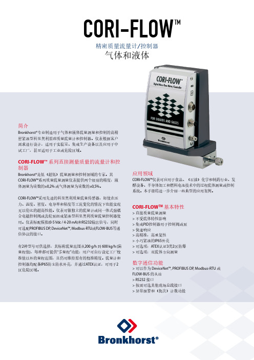
简介Bronkhorst®专业制造用于气体和液体流量测量和控制的高精密紧凑型科里奥利原理质量流量计和控制器。
仪表根据客户需求进行设计,适用于实验室、集成生产设备以及应用于中试工厂,甚至适用于工业或危险区域。
CORI-FLOW™系列直接测量质量的流量计和控制器Bronkhorst®是低(超低)流量测量和控制领域的专家。
其CORI-FLOW™系列质量流量测量仪表提供两个级别的精度:液体测量为读数的±0,2% 或气体测量为读数的±0,5%。
CORI-FLOW™采用先进的科里奥利质量流量传感器,即使在压力、温度、密度、电导率和粘度等工况变化的情况下也能实现无以伦比的超高性能。
仪表可做独立的流量计或同一体式强耦合电磁控制阀或齿轮泵组成紧凑型科里奥利质量流量控制器使用。
仪表标配模拟(0-5 Vdc / 4-20 mA)和RS232输出信号,同时可选配PROFIBUS DP, DeviceNet™, Modbus-RTU或FLOW-BUS等通信协议的接口。
有2种型号可供选择,其标称流量范围从200 g/h 到 600 kg/h (满量程值),每种都可提供“多量程”功能:用户可自行设定工厂校准值以外的量程范围,且仍可维持原有的校准精度。
流量计和控制器均配备IP65防尘防水外壳,并通过ATEX认证,可用于2区危险区域。
应用领域CORI-FLOW™仪表可应用于食品、(石油)化学和制药行业、发酵设备、半导体加工和燃料电池技术中的过程流体测量或控制系统。
本手册将进一步介绍一些典型的应用案例。
CORI-FLOW TM基本特性> 直接质量流量测量> 不受流体特性影响> 集成PID控制器用于控制阀或泵> 快速响应> 高精准,高重复性> 小巧紧凑的IP65外壳> 可选项:ATEX认证3类2区防爆> 可选项:双流体方向测量数字通信功能> 可以作为 DeviceNet™, PROFIBUS DP, Modbus-RTU 或FLOW-BUS 的从站> RS232 接口> 按需可选其他现场总线接口> 异常报警和(批次)计数功能CORI-FLOW TM 精密质量流量计/控制器气体和液体测量原理CORI-FLOW TM 包含两个平行的U 型管,形成振荡系统的一部分。
MB90F546GSPF中文资料

2
MB90540/540G/545/545G Series
(Continued) • UART 1 With full-duplex double buffer (8-bit length) Clock asynchronized or clock synchronized serial (extended I/O serial) can be used. • External interrupt circuit (8 channels) A module for starting an extended intelligent I/O service (EI2OS) and generating an external interrupt which is triggered by an external input. • Delayed interrupt generation module Generates an interrupt request for switching tasks. • 8/10-bit A/D converter (8 channels) 8/10-bit resolution can be selectively used. Starting by an external trigger input. Conversion time : 26.3 µs • FULL-CAN interfaces MB90540 series : 2 channel MB90545 series : 1 channel Conforming to Version 2.0 Part A and Part B Flexible message buffering (mailbox and FIFO buffering can be mixed) • External bus interface : Maximum address space 16 Mbytes • Package: QFP-100, LQFP-100
KROHNE OPTIWAVE 5400 C 24 GHz FMCW雷达液位计操作手册说明书

适用于基本过程工艺的24GHz FMCW 雷达液位计OPTIWAVE 5400 C操作手册© KROHNE 05/2018 - 4006972101 - MA OPTIWAVE 5400 R01 zh保留所有权。
未经KROHNE Messtechnik GmbH 公司事先书面授权,不得复制此文件及其任何部分。
如有更改,恕不通知。
205/2018 - 4006972101 - MA OPTIWAVE 5400 R01 zh版权所有 2018KROHNE Messtechnik GmbH - Ludwig-Krohne-Str. 5 - 47058 Duisburg (德国): 版本说明305/2018 - 4006972101 - MA OPTIWAVE 5400 R01 zh 1 安全须知61.1 软件历史.................................................................61.2 用途.....................................................................71.3 认证.....................................................................71.4 无线电批准证书.. (8)1.4.1 欧盟 (EU)...................................................................81.4.2 美国和加拿大 (10)1.5 来自制造厂家的安全须知 (13)1.5.1 版权及数据保护.............................................................131.5.2 免责条款...................................................................131.5.3 产品责任及质保.............................................................141.5.4 有关文档的信息.............................................................141.5.5 警告与符号使用.............................................................151.6 操作者的安全须知 (15)2 设备描述162.1 供货范围................................................................162.2 仪表说明................................................................172.3 外观检查................................................................182.4 铭牌.. (19)2.4.1 铭牌 (示例) (19)3 安装203.1 通用安装提示............................................................203.2 存储....................................................................203.3 运输....................................................................213.4 安装前要求..............................................................213.5 压力和温度范围..........................................................223.6 推荐的安装位置. (22)3.6.1 通用说明...................................................................233.6.2 具有盘状和锥形底部的储罐 (25)3.7 安装限制 (25)3.7.1 通用说明...................................................................253.7.2 过程连接...................................................................283.7.3 LPR 仪表:对于在井坑和非导电材质罐体的安装建议.............................323.7.4 立管(导波管和旁通管).....................................................333.8 如何连接天线延长管......................................................383.9 如何旋转或移除显示模块(选件)..........................................413.10 防护罩.. (42)3.10.1 如何将防护罩连接至仪表上..................................................423.10.2 如何打开防护罩 (44)4 电气连接454.1 安全须知................................................................454.2 常规注意事项............................................................454.3 电气安装:两线制,回路供电. (45)内容405/2018 - 4006972101 - MA OPTIWAVE 5400 R01 zh4.4 电流输出的电气连接 (49)4.4.1 非防爆仪表.................................................................494.4.2 用于危险区域的仪表 (49)4.5 防护等级................................................................494.6 网络.. (50)4.6.1 基本信息...................................................................504.6.2 点到点连接.................................................................504.6.3 多点网络. (51)5 启动525.1 启动检查列表............................................................525.2 如何启动仪表............................................................525.3 操作概念................................................................525.4 数显屏幕. (53)5.4.1 显示屏布局.................................................................535.4.2 键盘按钮. (54)5.5 通过PACTware ™远程通讯.................................................565.6 通过AMS ™设备管理器进行远程通讯. (57)6 操作586.1 用户模式................................................................586.2 常规模式................................................................596.3 程序模式. (62)6.3.1 常规注意事项...............................................................626.3.2 仪表设置保护(访问级别)...................................................626.3.3 如何访问快速设置菜单.......................................................646.3.4 键盘功能...................................................................656.3.5 如何保存程序模式中更改的设置...............................................686.3.6 菜单一览...................................................................696.3.7 功能说明...................................................................756.4 程序模式下仪表配置的更多信息 (91)6.4.1 标准设置...................................................................916.4.2 空频谱记录.................................................................946.4.3 HART ® 网络设置............................................................966.4.4 距离测量...................................................................976.4.5 物位测量...................................................................986.4.6 如何设置仪表测量体积或质量................................................1006.4.7 如何在弯曲或锥形底部的储罐中进行正确测量..................................1016.4.8 如何制作滤波器以去除雷达信号干扰 (102)6.5 状态消息和诊断数据 (103)7 服务1097.1 周期性维护 (109)7.1.1 常规注意事项..............................................................1097.1.2 维护外壳盖的O 形圈........................................................1097.1.3 如何清洁仪表的顶部表面....................................................1107.1.4 如何在过程条件下清洁喇叭天线..............................................1107.2 服务保修 (110)505/2018 - 4006972101 - MA OPTIWAVE 5400 R01 zh 7.3 备件可用性.............................................................1117.4 可提供的服务...........................................................1117.5 仪器送返生产厂家. (111)7.5.1 基本信息..................................................................1117.5.2 送返仪器时附带的表格(可复印).. (112)7.6 处理 (112)8 技术数据1138.1 测量原理...............................................................1138.2 技术数据...............................................................1158.3 测量精度...............................................................1218.4 最小供电电压...........................................................1228.5 最大操作压力指令.......................................................1238.6 尺寸和重量. (125)9 HART 接口1339.1 综述...................................................................1339.2 软件历史...............................................................1339.3 连接变量 (134)9.3.1 点到点连接 - 模拟/数字模式...............................................1349.3.2 多点连接 (2线制连接) (134)9.4 HART ® 仪表变量.........................................................1349.5 手操器 475 (FC 475)....................................................1359.5.1 安装......................................................................1359.5.2 操作. (135)9.6 资产管理系统 (AMS ®) (135)9.6.1 安装......................................................................1359.6.2 操作......................................................................1369.6.3 基本设置参数..............................................................1369.7 现场仪表工具 / 仪表类型管理器 (FDT / DTM) (136)9.7.1 安装......................................................................1369.7.2 操作. (136)9.8 过程设备管理(PDM)....................................................1369.8.1 安装......................................................................1369.8.2 操作. (136)9.9 AMD 的HART ®菜单结构 (137)9.9.1 AMS 菜单结构总览(菜单结构中的位置)......................................1379.9.2 AMS 菜单结构(具体设置)..................................................1379.10 PDM 的HART ® 树形菜单.. (140)9.10.1 PDM 菜单树总览(菜单树中的位置).........................................1409.10.2 PDM 菜单结构(具体设置). (141)10 附录14410.1 订货代码..............................................................14410.2 备件..................................................................15010.3 附件..................................................................15310.4 术语表. (153)1605/2018 - 4006972101 - MA OPTIWAVE 5400 R01 zh1.1 软件历史“固件版本符合”NAMUR NE 53。
M54HC245中文资料
M54HC245中文资料M54/74HC245/640/643M54/74HC245/640/643October 1993HC640INVERTING,HC643INVERTING/NON INVERTINGOCTAL BUS TRANSCEIVER (3-STATE):HC245NON INVERTING B1R(Plastic Package)ORDER CODES :M54HCXXXF1R M74HCXXXM1R M74HCXXXB1R M74HCXXXC1RF1R(Ceramic Package)M1R(Micro Package)C1R (Chip Carrier)PIN CONNECTION (top view).HIGH SPEEDt PD =10ns (TYP.)at V CC =5V .LOW POWER DISSIPATIONI CC =4μA (MAX.)at T A =25oC .HIGH NOISE IMMUNITYV NIH =V INL =28%V CC (MIN.).OUTPUT DRIVE CAPABILITY 15LSTTL LOADS.SYMMETRICAL OUTPUT IMPEDANCE |I OH |=I OL =6mA (MIN).BALANCED PROPAGATION DELAYS t PLH =t PHL.WIDE OPERATING VOLTAGE RANGE V CC (OPR)=2V TO 6V .PIN AND FUNCTION COMPATIBLE WITH 54/74LS245/640/643DESCRIPTIONThe M54/74HC245,HC640and HC643utilisesilicon gate C2MOS technology to achive operating speeds equivalent to LSTTL devices.Along with the low power dissipation and high noiseimmunity of standards C 2MOS integrated circuit,it possesses the capability to drive 15LSTTL loads.These IC’s are intended for two-way asynchronous communication between data buses,and the direction of data trasmission is determined by DIR input.The enable input (G)can be used to disable the device so that the buses are effectively isolated.All input are equippe d with protection circuits against staticdischarge and transient discharge and transient excess voltage.IT IS PROHIBITED TO APPLY A SIGNAL TO A BUS TERMINAL WHEN IT IS IN OUTPUT MODE AND WHEN A BUS THERMINAL IS FLOATING (HIGH IMPEDANCE STATE),IT IS REQUESTED TO FIX THE INPUT LEVEL BY MEANS OF EXTERNAL PULL DOWN OR PULL UP RESISTOR.HC245HC640HC6431/11INPUT AND OUTPUT EQUIVALENT CIRCUITPIN DESCRIPTIONPIN No SYMBOL NAME AND FUNCTION 1DIR Directional Control 2,3,4,5,6,7,8,9A1to A8Data Inputs/Outputs 18,17,16,15,14,13,12,11B1to B8Data Inputs/Outputs19G Output Enabel Input (Active LOW)10GND Ground (0V)20V CCPositive Supply VoltageIEC LOGIC SYMBOLSTRUTH TABLEINPUT FUNCTIONOUTPUT G DIR A BUS B BUS HC245HC640HC643L L OUTPUT INPUT A =B A =B A =B L H INPUT OUTPUTB =A B =A B =A HXZZZZZX:”H”or ”L”Z:High impeda nceHC245HC640HC643M54/M74HC245/640/6432/11M54/M74HC245/640/643 LOGIC DIAGRAM(HC640)NOTE:IN CASE OF HC245OR HC643,INPUT INVERTERS MARKED*AT A BUS AND B BUS ARE ELIMINATED RESPECTIVELY ABSOLUTE MAXIMUM RATINGSymbol Parameter Value Unit V CC Supply Voltage-0.5to+7V V I DC Input Voltage-0.5to V CC+0.5V V O DC Output Voltage-0.5to V CC+0.5VI IK DC Input Diode Current±20mAI OK DC Output Diode Current±20mAI O DC Output Source Sink Current Per Output Pin±35mAI CC or I GND DC V CC or Ground Current±70mAP D Power Dissipation500(*)mW T stg Storage Temperature-65to+150o C T L Lead Temperature(10sec)300o C Absolute Maximum Ratings are those values beyond whichdamage to the device may occu r.Functiona l ope ration und er these cond ition isnotimplied. (*)500mW:?65o C derate to300mW by10mW/o C:65o C to85o C3/11RECOMMENDED OPERATING CONDITIONSSymbol Parameter Value Unit V CC Supply Voltage2to6V V I Input Voltage0to V CC V V O Output Voltage0to V CC V T op Operating Temperature:M54HC SeriesM74HC Series -55to+125-40to+85o Co Ct r,t f Input Rise and Fall Time V CC=2V0to1000nsV CC=4.5V0to500V CC=6V0to400DC SPECIFICATIONSSymbol ParameterTest Conditions ValueUnit V CC(V)T A=25o C54HC and74HC-40to85o C74HC-55to125o C54HCMin.Typ.Max.Min.Max.Min.Max. V IH High Level InputVoltage 2.0 1.5 1.5 1.5V 4.5 3.15 3.15 3.156.0 4.2 4.2 4.2V IL Low Level InputVoltage 2.00.50.50.5V 4.5 1.35 1.35 1.356.0 1.8 1.8 1.8V OH High LevelOutput Voltage 2.0V I=V IHorV ILI O=-20μA1.92.0 1.9 1.9V 4.5 4.4 4.5 4.4 4.46.0 5.9 6.0 5.9 5.94.5I O=-6.0mA 4.18 4.31 4.13 4.106.0I O=-7.8mA 5.68 5.8 5.63 5.60V OL Low Level OutputVoltage 2.0V I=V IHorV ILI O=20μA0.00.10.10.1V 4.50.00.10.10.16.00.00.10.10.14.5I O=6.0mA0.170.260.330.406.0I O=7.8mA0.180.260.330.40I I Input LeakageCurrent 6.0V I=V CC or GND±0.1±1±1μAI OZ3State OutputOff State Current 6.0V I=V IH or V ILV O=V CC or GND±0.5±5.0μAI CC Quiescent SupplyCurrent 6.0V I=V CC or GND44080μAM54/M74HC245/640/643 4/11AC ELECTRICAL CHARACTERISTICS(C L=50pF,Input t r=t f=6ns)Symbol ParameterTest Conditions ValueUnit V CC(V)C L(pF)T A=25o C54HC and74HC-40to85o C74HC-55to125o C54HCMin.Typ.Max.Min.Max.Min.Max. t TLH t THL Output Transition Time2.05025607590ns4.571219186.06101315t PLH t PHL Propagation Delay Time2.0503390115135ns4.5121823276.0101520232.015048120150180ns4.5162430366.014202631t PZL t PZH Output Enable Time2.050R L=1K?48150190225ns4.5163038456.0142632382.0150R L=1K?63180225270ns4.5213645546.018313846t PLZ t PHZ Output DisableTime2.050R L=1K?37150190225ns4.5173038456.015263238C IN Input Capacitance DIR,G5101010pFC I/OUT OutputCapacitance An,Bn13pFC PD(*)Power DissipationCapacitanceHC245HC640/6433937pF(*)C PD is defined as the value of the IC’s internal equivalent capac itanc e which is calculated from the operating current con sump tion without load. (Refer to Test Circuit).Average opertingcurrent can be obtained by the following equ ation.I CC(opr)=C PD?V CC?f IN+I CC/8(per circuit)M54/M74HC245/640/6435/11SWITCHING CHARACTERISTICS TEST WAVEFORMTEST CIRCUIT I CC(Opr.)C PD CALCULATIONC PD is to be calculated with the followingformula by using the measured value of I CC(Opr.)in the test circuit opposite.C PD=I CC(Opr.)f IN x V CCM54/M74HC245/640/643 6/11M54/M74HC245/640/643 Plastic DIP20(0.25)MECHANICAL DATAmm inchDIM.MIN.TYP.MAX.MIN.TYP.MAX.a10.2540.010B 1.39 1.650.0550.065b0.450.018b10.250.010D25.4 1.000E8.50.335e 2.540.100e322.860.900F7.10.280I 3.930.155L 3.30.130Z 1.340.053P001J7/11M54/M74HC245/640/643Ceramic DIP20MECHANICAL DATAmm inch DIM.MIN.TYP.MAX.MIN.TYP.MAX.A250.984 B7.80.307D 3.30.130E0.5 1.780.0200.070 e322.860.900F 2.29 2.790.0900.110G0.40.550.0160.022I 1.27 1.520.0500.060L0.220.310.0090.012 M0.51 1.270.0200.050 N14°(min.),15°(max.)P7.98.130.3110.320 Q 5.710.225P057H 8/11M54/M74HC245/640/643SO20MECHANICAL DATAmm inchDIM.MIN.TYP.MAX.MIN.TYP.MAX.A 2.650.104a10.100.200.0040.007a2 2.450.096b0.350.490.0130.019b10.230.320.0090.012C0.500.020c145°(typ.)D12.6013.000.4960.512E10.0010.650.3930.419e 1.270.050e311.430.450F7.407.600.2910.299L0.50 1.270.190.050M0.750.029S8°(max.)P013L9/11M54/M74HC245/640/643PLCC20MECHANICAL DATAmm inch DIM.MIN.TYP.MAX.MIN.TYP.MAX.A9.7810.030.3850.395 B8.899.040.3500.356D 4.2 4.570.1650.180d1 2.540.100d20.560.022E7.378.380.2900.330e 1.270.050e3 5.080.200F0.380.015G0.1010.004 M 1.270.050M1 1.140.045P027A 10/11M54/M74HC245/640/643 Information furnished is believed to be accurate and reliable.However,SGS-THOMSON Microelectronics assumes no responsability for the consequences of use of such information nor for any infringement of patents or other rights of third parties which may results from its use.No license is granted by implication or otherwise under any patent or patent rights of SGS-THOMSONMicroelectronics.Specificationsmentioned in this publication are subject to change without notice.This publication supersedes and replaces all information previously supplied.SGS-THOMSON Microelectronics products are not authorized for use ascritical components in life support devices or systems without express written approval of SGS-THOMSON Microelectonics.1994SGS-THOMSON Microelectronics-All Rights Reserved SGS-THOMSON Microelectronics GROUP OF COMPANIESAustralia-Brazil-France-Germany-Hong Kong-Italy-Japan-Korea-Malaysia-Malta-Morocco-The Netherlands-Singapore-Spain-Sweden-Switzerland-Taiwan-Thailand-United Kingdom-U.S.A11/11。
W541U V2.0 用户手册
版权声明是深圳市吉祥腾达科技有限公司注册商标。
文中提及到的其它商标或商品名称均是他们所属公司的商标或注册商标。
本产品的所有部分,包括配件和软件,其版权属深圳市吉祥腾达科技有限公司所有,在未经过深圳市吉祥腾达科技有限公司许可的情况下,不得任意拷贝、抄袭、仿制或翻译成其它语言。
本手册中的所有图片和产品规格参数仅供参考,随着软件或硬件的升级会略有差异,如有变更,恕不另行通知,如需了解更多产品信息,请浏览我们公司网站:目录第一章产品简介 (1)1.1 产品特性 (1)1.2 产品应用 (2)1.3 安全警示 (3)1.4 指示灯描述 (3)1.5 物品清单 (3)第二章安装指南 (4)第三章客户端应用程序使用 (9)3.1 Station Mode (客户端模式) (10)3.2 AP Mode (17)附录 (22)附录一:相关技术名词解释 (22)附录二:产品规格 (24)附录三:设置PSP (25)第一章产品简介W541U V2.0无线USB网卡支持IEEE 802.11g、IEEE 802.11b标准,无线传输速率高达54Mbps。
W541U V2.0支持WPS一键加密功能,轻松保障您的无线网络安全;支持Soft AP 功能,方便您快速组建无线局域网;支持PSP、WII、NDS连接Internet及Xlink Kai,让您享受联网对战的乐趣;支持中文SSID,方便接入各种无线网络;真正支持WMM,让您的语音视频更流畅。
总之,W541U V2.0是一款信号好、传输距离远、性能稳定、性价比极高的11G无线网卡。
1.1产品特性●符合IEEE 802.11g、IEEE 802.11b标准;●提供USB2.0接口;●最大传输速度可达54Mbps;●自动侦测网络及变换传输速率;●提供两种工作模式:集中控制式(Infrastructure)和对等式(Ad-Hoc);●支持Soft AP功能,方便您快速组建无线局域网;●支持PSP、WII、NDS连接Internet及Xlink Kai,让您享受联网对战的乐趣;●支持64/128位WEP数据加密;支持WPA/WPA2等加密方式;●支持WPS一键加密功能,使您无须再记录烦琐的密码;●真正支持WMM,让您的语音视频更流畅;●支持中文SSID,更方便您的使用;1.2产品应用54M 无线网卡为无线访问提供快速、可靠、低成本的解决方法。
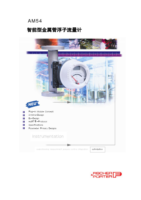
菲时博特AM54智能型金属管转子流量计-选型说明书
1000 1200 1800
80-250-K 10 80-250-K 20 80-250-K 30
DN100 ( 4〃)
63000 40000 100000 63000
2000 2500
100-250-K 10 100-250-K 20
DN150 ( 6〃)
100000 80000 160000 100000
流量QVn,则需要计算系数Fn:
根据以上计算的系数Fn,计算用空气标校时对应的空 气体积流量:QV(空气)=Fn×QVn
B、如果用户已知操作状态下的体积流量QVa,则需要计算
系数Fa:
根据以上计算的系数Fa,计算用空气标校时对应的空 气体积流量:QV(空气)=Fa×QVa
C、如果用户已知气体的质量流量QVm,则需要计算系数Fm:
垂直型浮子流量计安装示意图
根据以上计算的系数Fm,计算用空气标校时对应的空 气体积流量:QV(空气)=Fm×QVm
注: ρ1 =被测气体标准状态下密度 (Kg/m3) P1 =被测气体的绝对压力 (MPa) T1 =被测气体的绝对温度 (K) ρ2 =空气标准状态下密度 (1.293 Kg/m3) P2 =空气的绝对压力 (0.1013 MPa) T2 =空气的绝对温度 (293.15 K)
1. 概 述
Fischer&Porter公司的AM系列智能型金属管浮子流量计以其可变面积流量测量享誉全世界。其独特 的插入式指示器及多功能浮子等特点使本产品更加方便、可靠、完美。
本产品广泛应用于化工、石油、制药、食品和饮料等行业。 AM系列智能型金属管浮子流量计可测量液体、气体和水蒸汽,具有坚固、安全、耐用等特点。其耐 高压、高温等性能尤其适用于测量腐蚀性强、混浊、以及肮脏的液体。 测量管材质可多种选择,经检验可适用于多种恶劣工作环境。 指示器内附插入式模块,可在任何时候不中断测量随时升级更换,共有以下几种功能: ●AM-71带指针显示 ●AM-72带指针显示和下限报警 ●AM-73带指针显示和上限报警 ●AM-74带指针显示和上、下限报警 ●AM-31带指针显示,4-20mA信号输出 ●AM-32带指针和数字显示,4-20mA信号输出,数字能显示瞬时和累积流量,仪表参数现场可调。
Bosch HBL57M52UC builtin microwave 产品说明书
Oven
Bake, Variable Broil (hi & low),
modes – Roast, Warm, Sabbath, Proof
lower cavity Dough, Convection Bake,
Convection Broil, Convection
Roast, Pizza, Convection Multi-
Installation Details
Accessories: To purchase Bosch accessories, cleaners & parts please visit /us/store or call 1-800-944-2904 (Mon to Fri 5 am to 6 pm PST, Sat 6 am to 3 pm PST).
Electric
*
*Wall oven only
Dimensions & Weight
Overall appliance dimensions (HxWxD)
49" x 29 3/4" x 24 1/2"
Required cutout size – 48 5/8" x 28 1/2" x
Standard (HxWxD)
2,000 W
Technical Details
Watts
9,600 W
Circuit breaker
40 A
Volts; Frequency
240 / 208 V; 60 Hz
Power cord length
60"
Plug type
Fixed Connection, No Plug
C45002 产品手册说明书

浙江航芯源集成电路科技有限公司浙江航芯源集成电路科技有限公司Zhejiang HangXinYuan IC Technology Co.,LtdC45002 产品手册4通道逻辑门1.产品特性➢额定驱动电流:50mA ➢单芯片集成4通道➢具有输入反相逻辑配置位➢可实现双输入与门、与非门➢每个通道具备2个同相输出2.功能描述C45002是一款采用硅工艺制造的通用逻辑门芯片。
芯片具有4个通道,每个通道均可单独工作。
每个通道都具有输入反相逻辑配置位,使每个通道均可以实现与门或与非门逻辑,还可以配置为缓冲器、反相器。
输入引脚支持2.5V/3.3V/5V 逻辑电平,单个输出最大50mA 电流的驱动能力。
芯片还具备欠压保护功能。
3.典型应用➢缓冲器➢反相器➢电平位移4.裸芯片/封装简介➢本产品为裸芯片,尺寸为840μm*1590μm (含划片槽)有限公司5. 绝对最大额定值使用中超过这些绝对最大值可能对芯片造成永久损坏.6. 主要电参数无特别说明T A = -55℃~125℃,V DD =5V表 1 主要电参数浙江航路科公司7. 功能框图及引脚介绍7.1 功能框图IN1_1IN1_2CH1IN4_1IN4_2CH4IN3_1IN3_2CH3IN2_1IN2_2CH2OUT2_1OUT2_2OUT3_1OUT3_2OUT4_1OUT4_2GND图 1 功能框图268403606图 2 C45002引脚分布➢ 芯片尺寸:840μm×1590 μm (包含划片槽) ➢ PAD 尺寸:100μm×100μm表 2 C45002引脚说明科技有限公司8. 芯片应用说明0V0V 5V图 3 C45002典型应用图1) 4个通道相互独立,共电源共地,每个通道的两个输出为同相,且各个通道功能一致;2) 功率走线如电源、地、输出等,应简短并且具有一定的宽度;3) 多个VDD 和GND 内部已连接,但考虑到性能建议同时使用。
MC54HC4051中文资料

11 5 2 12 14
Control Inputs Enable L L L L L L L L H C L L L L H H H H X Select B A L L H H L L H H X L H L H L H L H X ON Channels Z0 Z0 Z0 Z0 Z1 Z1 Z1 Z1 Y0 Y0 Y1 Y1 Y0 Y0 Y1 Y1 NONE X0 X1 X0 X1 X0 X1 X0 X1
元器件交易网
MOTOROLA
SEMICONDUCTOR TECHNICAL DATA
Analog Multiplexers/ Demultiplexers
MC54/74HC4051 MC74HC4052 MC54/74HC4053
High–Performance Silicon–Gate CMOS
X0 14 X1 15 X2 ANALOG 12 MULTIPLEXER/ INPUTS/ X3 DEMULTIPLEXER OUTPUTS X4 1 5 X5 2 X6 4 X7 11 A CHANNEL 10 B SELECT 9 INPUTS C 6 ENABLE PIN 16 = VCC PIN 7 = VEE PIN 8 = GND
X SWITCH
X
ANALOG INPUTS/OUTPUTS
Y SWITCH
15
Y
COMMON OUTPUTS/INPUTS
Z SWITCH
4
Z
X = Don’t Care
PIN 16 = VCC PIN 7 = VEE PIN 8 = GND
MM54HC242中文资料
Absolute Maximum Ratings (Notes 1
2)
Operating Conditions
Supply Voltage (VCC) DC Input or Output Voltage (VIN VOUT) Operating Temp Range (TA) MM74HC MM54HC Input Rise or Fall Times (tr tf) VCC e 2 0V VCC e 4 5V VCC e 6 0V Min 2 0 Max 6 VCC Units V V
元器件交易网
MM54HC242 MM74HC242 Inverting Quad TRI-STATE Transceiver MM54HC243 MM74HC243 Quad TRI-STATE Transceiver
January 1988
MM54HC242 MM74HC242 Inverting Quad TRI-STATE Transceiver MM54HC243 MM74HC243 Quad TRI-STATE Transceiver
Features
Y Y Y Y Y Y
Typical propagation delay 12 ns TRI-STATE outputs Two way asynchronous communication High output current 6 mA (74HC) Wide power supply range 2 – 6V Low quiescent supply current 80 mA (74HC)
g0 5
g5 0
g 10
80
801Biblioteka 0Note 1 Absolute Maximum Ratings are those values beyond which damage to the device may occur Note 2 Unless otherwise specified all voltages are referenced to ground Note 3 Power Dissipation temperature derating plastic ‘‘N’’ package b 12 mW C from 65 C to 85 C ceramic ‘‘J’’ package b 12 mW C from 100 C to 125 C Note 4 For a power supply of 5V g 10% the worst case output voltages (VOH and VOL) occur for HC at 4 5V Thus the 4 5V values should be used when designing with this supply Worst case VIH and VIL occur at VCC e 5 5V and 4 5V respectively (The VIH value at 5 5V is 3 85V ) The worst case leakage current (IIN ICC and IOZ) occur for CMOS at the higher voltage and so the 6 0V values should be used VIL limits are currently tested at 20% of VCC The above VIL specification (30% of VCC) will be implemented no later than Q1 CY’89
MSM54V32126A中文资料

(Ta = 0°C to 70°C)
Max.
Unit
3.6
V
0
V
3.6
V
0.3
V
Typ. — —
(VCC = 3.3 V ±0.3 V, Ta = 25°C, f = 1 MHz)
Max.
Unit
7
pF
7
pF
4/26
元器件交易网
¡ Semiconductor
MSM54V32126A
tHPC = Min.
— 150 — 140 — 135 mA 1, 2, 4
Average Power
Supply Current (CAS before RAS Refresh)
ICC5
RAS = cycling, CAS before RAS
— 140 — 130 — 110 mA 1, 2, 4
Parameter Input Capacitance Input / Output Capacitance
Symbol CIN CIO
Rating
Unit
–0.5 to 4.5
V
50
mA
1
W
0 to 70
°C
–55 to 150
°C
Min. 3.0 0 3.0 –0.3
Typ. 3.3 0 — —
Note:
Pin Name
A0 - A8 DQ0 - DQ31
RAS CAS1 - CAS4
WE OE
VCC VSS NC
Function Address Input Data Input / Data Output Row Address Strobe Column Address Strobe Write Enable Output Enable Power Supply (3.3 V) Ground (0 V) No Connection
CD54HC00H中文资料

CD74HCT00M96
-55 to 125
14 Ld SOIC
NOTE: When ordering, use the entire part number. The suffix 96 denotes tape and reel. The suffix T denotes a small-quantity reel of 250.
• Wide Operating Temperature Range . . . -55oC to 125oC
The CD54HC00, CD74HC00, CD54HCT00, and CD74HCT00 logic gates utilize silicon gate CMOS technology to achieve operating speeds similar to LSTTL gates with the low power consumption of standard CMOS integrated circuits. All devices have the ability to drive 10 LSTTL loads. The 74HCT logic family is functionally pin compatible with the standard 74LS logic family.
• HC Types - 2V to 6V Operation - High Noise Immunity: NIL = 30%, NIH = 30% of VCC at VCC = 5V
• HCT Types - 4.5V to 5.5V Operation - Direct LSTTL Input Logic Compatibility, VIL= 0.8V (Max), VIH = 2V (Min) - CMOS Input Compatibility, Il ≤ 1µA at VOL, VOH
RRH_BDPAD701M54-1A-2英文产品规格书_RRH交直流转换概论

BDPAD701M54-1A-2Customized Power SupplyInput:85-285VacOutput Power: 700WApplications48V Distributed power systemEthernetExchangeLAN, MANServerIndoor and outdoor wireless networkTelecom equipmentForewordWelcome to use BDPAD701M54-1A-2 customized power supply from Shanghai Beidian, which is provided with extended input voltage. The power supply normally works with 90-290VAC input, -54V single output. Protections against short-circuit, over-current, over-voltage and input under voltage are functional. The power supply is designed strictly in accordance with the safety regulations, which conforms to the safety standards and requirements of information technological equipment.Safety rules:Any touch with bare hand against high voltage at input side is forbidden.High voltage!The device shall be securely grounded before power-on.CautionAny operation at AC & high voltage under lightning is forbidden.High voltage!1. SpecificationsEnvironmental requirementsParameters Min Typ.Max Unit Remark Operating temp -40 25 55 °CStorage temp -40 25 65 °CHumidity 5 95 %Altitude 0 4000 m Max temperature at sea level is 65°C, it will be derated by 1.5°C per 1000m.Atmospheric pressure 60 106 KPaCooling Convectional coolingInputParameter Min.Typ Max.Unit RemarksInput Voltage Range 85 110/220 285 Vac Damage free under long-term 320V input Input Frequency 47 50/60 63 HzInput Current 13 A Input 150-285Vac, output:700WInrush Current 30 A 220V Input (ETS 300 132-1)Power Factor 0.95 Rated input/rated loadAC Input Single phase, three wires 110Vac/220Vac single phase, 110Vac double live line inputOutputParameter Min.Typ.Max.Unit Remarks Output Voltage Range -52 -54 -56 VdcOutput Current Range 13 ALoad regulation ±1 %Regulation ±2 %Line regulation ±1 %Ripple (Vp-p) 200 mV Rated input/output, with 0.1uF ceramic capacitor and 10uF high frequency electrolyte capacitor, oscilloscope band width of 20MHz.Output Power 700W-40°C to 65°C,wind speed =0 m/s500 55°C to 70°C, MAX,wind speed =0 m/s)Efficiency >91 % At the load >70% (220V input &25℃)>88 % At the load >50% (220V input &25℃)Hold up time 10 mS Normal input of 220Vac &output of 550wOver/under shoot @ start up/shutdown ±5 %Full voltage, full load to min load, nocapacitive loadTransient response overshoot ±5 %Load variation:25%-50%-25% or 50%-75%-50%Recovery time fortransient response200 usTemperaturecoefficient±0.02 %/℃Output keep-up time 10 ms 220Vac input, full load output1. SpecificationsProtectionsParameterMin.Typ.Max.UnitRemarksInput under-voltage78VAuto recoverableInput under-voltagerecovery set point85VHysteresis not less than 5VInput over-voltage 290VAuto recoverableInput over-voltagerecovery set point 285VHysteresis not less than 5VOutput over-voltageprotection set point 5860VOutput current limiting15 18 A Auto recoverableShort circuit A Long-term short circuit endurable; Auto recoverableThermal protection100℃Auto recoverable under ambient temperature of 60℃.Safety & Insulation ratingParameter RequirementRemarksSafetyDesign in compliance with UL60950-1,EN60950-1,IEC60950-1,UL50and EN60950-22; TUV, UL, CE certifiedInput - output 3000Vac (4242Vdc)/10mA//1min No flashover or breakdownThe discharge tube shall be removed during test.Input-ground 1500Vac (2121Vdc_/10mA//1min Output - ground 500Vdc (700Vdc)/10mA//1minLeakage current<3.5mA264Vac Input 50Hz InputInsulation resistance ≥10MΩ@ normal atmospheric pressure,relative humidity: 90% Testing voltage: 500v dc insulation of input-output,input-ground, output-ground shall not be less than 10MΩ Safety approvalSatisfy requirements of IEC60950, UL60950and GB4943-2001; UL, TUV, CE and 3C certified.UL60950-1; EN60950-1 IEC60950-1; GB4943-20011. SpecificationsEMC and other parametersParameters StandardConducted emission EN55022 - Class B Radiated emission EN55022 - Class BESD EN/IEC 61000-4-2 EN55024Contact discharge:±8KV Air discharge:±15KV Criterion B (Discharge the enclosure after chassis is equipped)North America: Contact discharge: ±8KV,Air discharge:±15KVHarmonic emission EN/IEC61000-3-2 CLASS ACS EN/IEC 61000-4-6 LEVEL 3;10V/m,80%AM Criterion A RS EN/IEC 61000-4-3 LEVEL 3;10V/m,80%AM Criterion AEFT EN/IEC 61000-4-4 ±2 KV Criterion AB; North America: earthing terminal ±4 KVSURGE Line to line: 1.2/50us&8/20us, +/- 6kV@3kALine to GND: 1.2/50us&8/20us, +/- 6kV@3kADIP EN/IEC61000-4-11 Dip to 70%UT, duration: 100ms Dip to 40%UT, duration: 20ms,Dip to 0%UT, duration: 10msDIP at 0°, 45°, 90°, 135°, 180°, 225°, 270°, 315°As per criterion B;Others as per criterion BVoltage ripple & flicker EN/IEC61000-3-3 Pst≤1.0; P1t≤0.65; dc≤3.3%; dmax≤4%; time for d(t) exceeds 3%≤500msLightning proof AC input side can endure 8/20us impacting current, differential mode: 6KA common mode: 6KAReliability (calculated) ≤100,000 Hours (air inlet temperature 25°C) Service life ≥10 yearsRepair rate ≤1%Vibration Routine environment test: 5- 9Hz; Amplitude 3.5mm; 9-200Hz; acceleration spectral density: 10m2/s3 ; 3 directions, frequency sweep 5 times per direction (3*50 minutes) Package & transportation test: 5-20Hz, 1.0m2/s3; 20-200Hz: -3dB; 0.781Grms, 3 directions, 30 minute per directionShock Routine environment test: Half-sine wave, acceleration: 20G, pulse width: 11ms; Directions: X, Y, Z 3 times per directionPackage & transportation test: Half-sine wave, acceleration: 300m/s2, pulse width: 6ms; 6 directions, 3 times per directionBump Routine environment test: Half-sine wave, acceleration: 20G, pulse width: 11ms; Directions: X, Y, Z 3 times per directionPackage & transportation test: Half-sine wave, acceleration: 180m/s2, pulse width: 6ms; 6 directions, 100 times per directionDrop Routine environment test: Weight<10Kg, 10-25Kg, 25-50kg, ≥50kg, height:0.10m, 0.075m、0.05m、0.025m, drop at S1, E1, E3, angle C, C2Package & transportation test: Drop at surface, angle, and edge; weight 50-100Kg, 40-50Kg, height:30cm, 40cmSalt Fog Exposure The ACDC power supply shall show no signs of red or white corrosion after 720-hour exposure under standard salt fog conditions.Acoustic noise <55dBACooling 1 Natural cooling @ 65 ℃without wind, 60W (30W per output);2 Cooling by wind through air ducts, 0.5m/s Odor No peculiar and deleterious odor IP rating IP652. Mechanical parametersMechanical specifications Length*Width*Height358.98 mm *179.98 mm *79.37mmWeight (kg) ≤6Kg ColorGRAY OS11523Output connector :Input connector :4-?72-M 616616338,5179,9890110124.579,37+0,6-0358,982. Mechanical parameters1、Interface description:Pin No. SignalOutput connector (DC-out) 1 -48V2 BRTRN3 ShieldingInput connector (AC-in) A NB GNDC LAlarm output 3 Alarm8 Alarm RTN2、Alarm UnitAlarm unit for input low voltage and over voltage detection should be provided.If the input voltage is lower than 85VAC or higher than 280VAC, the alarm unit should output one alarm signal.After that signal, the PSU should keep normal operation before shutdown at least 0.6mS.Opendrain optocoupler with more than 1mA pull-down current capability is suggested. For details, refer to below figure.ALARM output:“CLOSE”: input voltage is not satisifed and shortcut the alarm output (<10 ohm)“OPEN”: input voltage is satisifed and cut the alarm output3、Input protectionsThe PSU shall not be damaged by the continuous application of AC input voltages within the abnormal range.•Input low voltage protectionThe PSU shall provide input low voltage protection by shutting down and restarting automatically at Requirement Min Nom Max UnitsStartup and Shutdown 80 84 VrmsHysteresis 1V Vrms2. Mechanical parameters•Input over voltage protectionThe PSU shall provide input Over voltage protection by shutting down and restarting automatically at the limits specified in below table.Requirement Min Nom Max UnitsStartup and Shutdown 281 290 VrmsHysteresis 1V Vrms3、Output connector wire:1000±20mm4、AccessoryNo. Name Model Quantity Unit1 Spring washer M6 4 pcs2 Flat washer M6 4 pcs3 Sunken hexagonal bolt M6X124 pcsRemark: The above material is stainless steel.3.1 UnpackingCheck the equipment, and make sure they are not damaged in transport. Keep the package until all of the modular units in the power equipment are registered and checked.3.2 General rules● The air passage of the modular unit should not be blocked.● The distance between the conductive part and metal component in the power equipment should conform to therelevant standards.3.3 Notes concerning damaged security protection● Once the security protection of the equipment is damaged, the equipment must stop operation and handledaccording to the relevant maintenance regulations.● When the power equipment is moved from a cold environment to a warm environment, condensation may lead tohazard issues, so the equipment should be grounded strictly according to the grounding requirements. Only qualified personnel can connect the equipment to the electrical supply.● After power cut off, wait four minutes to allow sufficient capacitor discharge before maintenance of the powerequipment.3.4 Notices● To operate u nder the environmental conditions in the Specification;● Forbid to adjust potentiometer without authority;● Switching power supply should be in the good cooling conditions -operating; it should be shut off if there is smokeor odor at turn on or operation.3.5 PackageOn the packing box, there are product name, model, manufacturer logo, quality certificate, and date of production, etc. In the packing box, there are specification and accessory list.3.6 TransportThis product is suitable for land, water, and air transport. In the transport, the product should be covered, protected against direct sunlight, and handled with care.3.7 StorageWhen the product is not in use, it should be placed in the packing box in an warehouse with an ambient temperature of -45~+70℃and relative humidity of 0%~95%. The warehouse should be free of harmful gas, inflammable, explosive or corrosive items, and should also be free of intense mechanical vibration, impact and intense magnetic field. The packing box should be padded at least 20cm high above the ground, and at least 50cm away from the wall, heat source, or window-type air inlet. Under the above storage conditions, the storage duration is 2 years. After that, the product should be tested again.3.8 Time Limit of WarrantyIn 1 year warranty, we provide free maintenance for all natural damages under normal operation conditions, except● Damages resulting from unauthorized maintenance;● Unauthorized addition or modif ication;● Incorrect operations and use;● Damages resulting from exposure to the abnormal ambient conditions that are not stipulated in the specifications;● Deliberate destruction on the system; and● Force majeure damages.3.9 Scope of WarrantyIn time limit of warranty, our Company can maintenance for free for the abnormal caused by the fault of materials and manufacture technique. The scope of warranty include labor server and any necessary adjustment and replace of components.3.10 Operational Safety GuidancePlease be sure to observe the following rules of security stipulated at any time, such as operation, cleaning and maintains. If there is any deregulation beyond the rules, our Company is with responsibility for mistakes caused by deregulations.● Forbid operate in conditions with volatility gas and flammability.● Forbid uninstall case and touch inside components at any time● For the sake of safety, forbid do inside maintenance and replace components by self.3.11 Cited standards●GB/T 2423.1-2001 Ambient test for Electronic and Electric Product Part2: Test method Test A: Lowtemperature●GB/T 2423.2-2001 Ambient test for Electronic and Electric Product Part2: Test method Test B: Hightemperature●GB/T 2423.9-2001 Ambient test for Electronic and Electric Product Part2: Test method Test Cb: Constanttemp. and humidity●GB/T 2423.10-1995 Ambient test for Electronic and Electric Product Part2: Test method Test Fc andGeneral: Vibration (Sine)●GB 4943-2001 Security of IT Apparatus●DIN ETS 300019-1-1-1993 Equipment Research Ambient Condition and Ambient Test forTelecommunication Equipment Part 1-1 Ambient condition: Long-term Storage●DIN ETS 300019-1-2-1993 Equipment Research Ambient Condition and Ambient Test forTelecommunication Equipment Part 1-2 Ambient condition: Transportation●GJB 1443-1992 Requirements on Product Package, Handling, Transport and Storage●GB/T 3873-1983 General Specifications for Communication-purpose Product PackageHigh Power DensityBDPAD701M54-1A-2 Customized Power Supply 3. SAFETY●GB/T 2423.3-1993 Ambient test for Electronic and Electric Product Test Ca: Constant temp. and humidity●GB 15842-1995 Safety Requirement and Testing Method for Mobile Communication Power Supply●GB/T 13722-92 Technical Requirement and Testing Method for Mobile Communication Power Supply●Q/ZX 23.011.5-2004 Requirements on EMC Test of Communication-purpose Power Supply●Q/ZX 23.018.1-2001 Requirements on Reliability Test -General●Q/ZX 23.011.1-2004 Requirements on EMC Test of Communication-purpose apparatus -General●YD/T 731—2002 Communication-purpose HF Switching Rectifier●ETSI 300 019 Environmental Engineering (EE); Environmental Conditions and Environmental Tests forTelecommunications Equipment●ETSI EN 301 489-1 Electromagnetic Compatibility and Radio spectrum Matters (ERM); ElectromagneticCompatibility (EMC) Standard for Radio Equipment and Services; Part 1: Common Technical Requirements●ETSI EN 301 489-8 Electromagnetic Compatibility and Radio Spectrum Matters(ERM); ElectromagneticCompatibility (EMC) Standard for Radio Equipment and services; Part 8: Specific Conditions for GSM Base Stations●BS EN 55022 Limiting Value and Measuring Method for Information Technology Equipment●CEI IEC 60950-1999 Safety of Information Technology Equipment●UL 60950 Safety of Information Technology Equipment●IEC61000-4 Electromagnetic Compatibility (EMC); part 4: Testing and Measurement Techniques●IEC 60529 AMD 1-1999 Degrees of Protection Provided by Enclosures(IP code); Amendment 1Page 3 of 11。
理工毕业论文铁电存储器FM18L08在DSP系统中的应用
铁电存储器FM18L08在DSP系统中的应用[关键词] DSP;铁电存储器;并行引导装载模式1 引言铁电存储器(FRAM)是Ramtron公司近年推出的一款掉电不挥发存储器,它结合了高性能和低功耗操作,能在没有电源的情况下保存数据。
FRAM克服了EEPROM和FLASH写入时间长、擦写次数低的缺点,其价格又比相同容量的不挥发锂电SRAM低很多,已在地铁系统、抄表系统及IT工业中得到了广泛的应用。
TMS320VC5402(以下简称C5402)是美国德州仪器公司(TI)推出的一款性价比极高的16bit定点数字信号处理器(DSP),操作速率可达100MIPS,它丰富的内部资源配置为用户构造系统提供了很大便利,已经在通信、电子、图象处理等领域得到了广泛的应用。
但是,C5402是RAM型器件,掉电后不能保持任何用户信息,所以需要用户把程序代码放在不挥发的存储器内,在系统上电时,通过执行自行引导装载(Bootloader)程序将存储在外部媒介中的代码装载到C5402高速的片内存储器或系统中的扩展存储器内,装载成功后自动去执行代码,完成自启动。
基于实践经验,本文介绍了一种并行接口铁电存储器FM18L08的特点,同时还分析了C5402 并行引导装载模式的特点,给出了一种基于铁电存储器FM18L08和C5402接口的设计方案, 实现了基于并行引导装载模式的DSP脱机独立运行系统设计,并且该设计方案已成功的应用到一种语音门锁系统中。
2 FM18L08 FRAM的特点Ramtron’s FRAM存储器技术的核心是微小的铁电晶体集成到记忆体单元,以至于它能象快速的不挥发RAM一样操作。
当一个电场被加到铁电晶体,中心原子顺着电场的方向移动。
移去电场,中心原子保持不动,保存记忆体的状态, FRAM 记忆体不需要定期刷新,掉电后立即保存数据。
FM18L08是Ramtron公司近年推出的一款存储容量为32k╳8bits FRAM,其主要特点如下:3.0-3.65V单电源供电;并行接口;提供SOIC和DIP两种封装;功耗低,静态电流小于15uA,读写电流小于10mA;非挥发性,掉电后数据能保存10年;读写无限次。
JMV中科电M5543电子版说明书

JMV中科电M5543电子版说明书特别提示由于视频格式编码种类很多,因此本机无法保证对所有格式的视频保持良好的兼容性,如碰到兼容性问题时,请使用转换软件。
一、前言首先对您使用JMV中科电数码产品表示感谢!本机是全新一代的数码MP5产品,其有着完美的视听功能与极高的可靠性和精巧的外观相得益彰,堪称大师级的作品,衷心的希望她能给您带来数码时代的超凡享受。
在首次使用之前请务必详细阅读此说明书。
读完后请将说明书保存好,为以后需要时做参考之用。
为了更好的服务,本用户手册的内容可能变更。
因为产品的性能和功能而发生的变更,将不做另行通知。
如果产品的实际设置和使用方法与本手册不一致,请以机器为准或请访问本公司网站查询最新产品信息。
◆本机型有多种外观,风格不尽相同,请以实物为准。
◆本机型有多种菜单界面,风格不尽相同,功能不变,请以机器演示为准。
◆本产品软件、硬件及说明书有任何修改,恕不另行通知,本公司拥有最终解释权。
二、注意事项在使用本产品之前,请务必注意下列事项:(1)、不要在特别冷、热、多尘和潮湿的环境中使用。
(2)、请避免将机器放置于阳光直射的地方(如停在空旷地带的车辆、沙滩上等等)。
(3)、不要让本机与硬物摩擦撞击,否则会导致本机表面磨花或其它硬件损坏。
(4)、扩展卡插入、拔出均要注意关机操作,因为插拔时电流很大,会给机器造成不可预测的损坏。
(5)、尽量放置在儿童触摸不到的地方,以防止碰落或磕上尖锐物体造成严重的损坏。
(6)、在下列情况下请对电池充电:A、电池电量图标为空,并闪动。
B、系统自动关机,再次开机后很快关机。
(7)、尽量避免在特别干燥的环境下使用,以防静电。
(8)、本机在格式化或正在进行文件的上传下载时不要突然断开连接,否则可能会导致程序出错。
(9)、本机被作为移动磁盘时,用户请按正确文件管理操作方法存储导出文件,重要数据请做好备份,任何错误操作方法导致文件丢失,本公司概不负责。
(10)、本机由高精密度配件组成,请勿随意自行拆卸、分解本机。
M54HC245D中文资料
M54HC245D中文资料1/10April 2004sHIGH SPEED:t PD =10ns (TYP .)at V CC =6V sLOW POWER DISSIPATION:I CC =4μA(MAX.)at T A =25°C sHIGH NOISE IMMUNITY:V NIH =V NIL =28%V CC (MIN.)sSYMMETRICAL OUTPUT IMPEDANCE:|I OH |=I OL =6mA (MIN)sBALANCED PROPAGATION DELAYS:t PLH ?t PHLsWIDE OPERATING VOLTAGE RANGE:V CC (OPR)=2V to 6VsPIN AND FUNCTION COMPATIBLE WITH 54SERIES 245s SPACE GRADE-1:ESA SCC QUALIFIED s50krad QUALIFIED,100krad AVAILABLE ON REQUESTsNO SEL UNDER HIGH LET HEAVY IONS IRRADIATIONsDEVICE FULLY COMPLIANT WITH SCC-9405-013DESCRIPTIONThe M54HC245is an advanced high-speed CMOS OCTAL BUS TRANSCEIVER (3-STATE)fabricated with silicon gate C 2MOS technology.This IC is intended for two-way asynchronouscommunication between data buses,and the direction of data transmission is determined by DIR input.The enable input G can be used to disable the device so that the buses are effectively isolated.All inputs are equipped with protection circuits against static discharge and transient excess voltage.All floating bus terminals during High Z State must be held HIGH or LOW.M54HC245RAD-HARD OCTAL BUS TRANSCEIVER WITH 3STATE OUTPUTS (NONINVERTED)PIN CONNECTIONORDER CODESPACKAGE FM EM DILC M54HC245D M54HC245D1FPCM54HC245KM54HC245K1M54HC2452/10IEC LOGIC SYMBOLSINPUT AND OUTPUT EQUIVALENT CIRCUIT PIN DESCRIPTIONTRUTH TABLEX :Don’t CareZ :High ImpedancePIN N°SYMBOL NAME AND FUNCTION 1DIR Directional Control 2,3,4,5,6,7,8,9A1to A8Data Inputs/Outputs 18,17,16,15,14,13,12,11B1to B8Data Inputs/Outputs19G Output Enable Input 10GND Ground (0V)20V CCPositive Supply VoltageINPUTSFUNCTIONOUTPUT G DIR A BUS B BUS Yn L L OUTPUT INPUT A =B L H INPUT OUTPUTB =A HXZZZM54HC2453/10ABSOLUTE MAXIMUM RATINGSAbsolute Maximum Ratings are those values beyond which damage to the device may occur.Functional operation under these conditions is not impliedRECOMMENDED OPERATING CONDITIONSSymbol ParameterValue Unit V CC Supply Voltage -0.5to +7V V I DC Input Voltage -0.5to V CC +0.5V V O DC Output Voltage -0.5to V CC +0.5V I IK DC Input Diode Current ±20mA I OK DC Output Diode Current ±20mA I O DC Output Current ±35mA I CC or I GND DC V CC or Ground Current±70mA P D Power Dissipation 420mW T stg Storage Temperature -65to +150°C T LLead Temperature (10sec)265°CSymbol ParameterValue Unit V CC Supply Voltage 2to 6V V I Input Voltage 0to V CC V V O Output Voltage 0to V CC V T op Operating Temperature -55to 125°C t r ,t fInput Rise and Fall TimeV CC =2.0V 0to 1000ns V CC =4.5V 0to 500ns V CC =6.0V0to 400nsM54HC2454/10DC SPECIFICATIONSSymbolParameterTest ConditionValue UnitV CC (V)T A =25°C -40to 85°C -55to 125°C Min.Typ.Max.Min.Max.Min.Max.V IHHigh Level Input Voltage 2.0 1.5 1.5 1.5V 4.5 3.15 3.15 3.156.0 4.24.24.2V ILLow Level Input Voltage2.00.50.50.5V4.5 1.35 1.35 1.356.0 1.81.81.8V OHHigh Level Output Voltage2.0I O =-20μA 1.9 2.0 1.9 1.9V4.5I O =-20μA 4.4 4.5 4.4 4.46.0I O =-20μA5.96.0 5.9 5.94.5I O =-6.0mA 4.18 4.31 4.13 4.106.0I O =-7.8mA 5.685.8 5.635.60V OLLow Level Output Voltage2.0I O =20μA 0.00.10.10.1V 4.5I O =20μA 0.00.10.10.16.0I O =20μA 0.00.10.10.14.5I O =6.0mA 0.170.260.330.406.0I O =7.8mA 0.180.260.330.40I I Input Leakage Current6.0V I =V CC or GND ±0.1±1±1μA I OZ High Impedance Output Leakage Current6.0V I =V IH or V IL V O =V CC or GND ±0.5±5±10μA I CCQuiescent Supply Current6.0V I =V CC or GND44080μAM54HC2455/10AC ELECTRICAL CHARACTERISTICS (C L =50pF,Input t r =t f =6ns)CAPACITIVE CHARACTERISTICS1)C PD is defined as the value of the IC’s internal equivalentcapacitance which is calculated from the operating current consumption without load.(Refer to Test Circuit).Average operating current can be obtained by the following equation.I CC(opr)=C PD x V CC x f IN +I CC /8(per circuit)SymbolParameterTest ConditionValue UnitV CC (V)C L (pF)T A =25°C -40to 85°C -55to 125°C Min.Typ.Max.Min.Max.Min.Max.t TLH t THL Output TransitionTime 2.05025607590ns 4.571219186.06101315t PLH t PHL Propagation DelayTime2.0503390115135ns4.5121823276.010*******.015048120150180ns4.5162430366.014202631t PZL t PZH High ImpedanceOutput Enable Time2.050R L =1K ?48150190225ns4.5163038456.0142632382.0150R L =1K ?63180225270ns4.5213645546.018313846t PLZ t PHZ High ImpedanceOutput Disable Time2.050R L =1K ?37150190225ns4.5173038456.015263238SymbolParameterTest ConditionValue UnitV CC (V)T A =25°C -40to 85°C -55to 125°C Min. Typ.Max.Min.Max.Min.Max.C IN Input Capacitance DIR,G 510 1010pF C I/OUT OutputCapacitanceAn,Bn13pF C PDPower Dissipation Capacitance (note 1) 39pFM54HC2456/10TEST CIRCUITC L =50pF/150pF or equivalent (includes jig and probe capacitance)R 1=1K ?or equivalentR T =Z OUT of pulse generator (typically 50?)WAVEFORM 1:PROPAGATION DELAY TIME (f=1MHz;50%duty cycle)TESTSWITCH t PLH ,t PHL Opent PZL ,t PLZ V CC t PZH ,t PHZGNDM54HC2457/10WAVEFORM 2:OUTPUT ENABLE AND DISABLE TIME (f=1MHz;50%dutycycle)M54HC245DILC-20 MECHANICAL DATAmm.inch DIM.MIN.TYP MAX.MIN.TYP.MAX.A 2.1 2.710.0830.107a1 3.00 3.700.1180.146 a20.630.88 1.140.0250.0350.045B 1.93 2.03 2.230.0760.0800.088b0.400.450.500.0160.0180.020b10.200.2540.300.0080.0100.012 D25.1425.4025.650.990 1.000 1.010 e7.367.627.870.2900.3000.310 e1 2.540.100e222.7322.8622.990.8950.9000.905e37.627.878.120.3000.3100.320 F7.297.497.700.2870.2950.303I 3.860.152K11.3011.560.4450.455 L 1.14 1.27 1.400.0450.0500.0550016178J 8/10M54HC2459/10DIM.mm.inchMIN.TYP MAX.MIN.TYP.MAX.A 9.9810.1610.340.3930.4000.407B 9.9810.1610.340.3930.4000.407C 1.45 1.61 1.780.570.630.070D 0.100.1270.180.0040.0050.007E 11.3011.4311.560.4450.4500.455F 1.270.050G 0.380.430.480.0150.0170.019H 7.248.160.2850.320L 24.4626.670.960 1.050M 0.450.500.550.0180.0200.022N 7.870.310O 1.14 1.27 1.400.0450.0500.055P0.100.180.250.0040.0070.010FPC-20 MECHANICAL DATA016032FM54HC245Information furnished is believed to be accurate and reliable. However, STMicroelectronics assumes no responsibility for the consequences of use of such information nor for any infringement of patents or other rights of third parties which may result from its use. No license is granted by implication orotherwise under any patent or patent rights of STMicroelectronics. Specifications mentioned in this publication are subject to change without notice. This publication supersedes and replaces all information previously supplied. STMicroelectronics products are not authorized for use as critical components in life support devices or systems without express written approval of STMicroelectronics.The ST logo is a registered trademark of STMicroelectronics All other names are the property of their respective owners 2004 STMicroelectronics - All Rights ReservedSTMicroelectronics GROUP OF COMPANIESAustralia - Belgium - Brazil - Canada - China - Czech Republic - Finland - France - Germany - Hong Kong - India - Israel - Italy - Japan - Malaysia - Malta - Morocco - Singapore - Spain - Sweden - Switzerland - United Kingdom - United States.10/10。
费尔奇公司双臂锚杆机CHDDR-2

CRAWLER CHASSIS 履带式车体
Safety Features of the Chassis 车体安全特性
• Center “Walk-Thru” design keeps the operators away from the dangers of the side-walls. • 中部通过式设计使操作者更安全。 中部通过式设计使操作者更安全。 • Ground Clearance – 305mm • 离地间隙-305毫米 离地间隙-305毫米 • Flat cover plating, and operator trays, allows for large storage of consumables, and prevents people having to work from the side of the machine. • 物料盘能够存放大量易耗件,同时操作 物料盘能够存放大量易耗件, 位置可以使操作员在锚杆工作中始终处 于机身保护范围内。 于机身保护范围内。
Muffler 消声器
Pipe Layout
Hydraulic Drill Canopies. 液压高度调节式顶棚
• Hydraulic Canopies protect the operator when bolting. • 液压调节顶棚在打锚杆时保护操作员。 液压调节顶棚在打锚杆时保护操作员。 • All canopies have MSHA Certification, (that means they can withstand a static load of 8.2 tonnes, yet still remain within their elastic state). • 所有顶棚均通过 所有顶棚均通过MSHA认证(即顶棚在自身弹 认证( 认证 性范围内能够承受8.2吨的静载荷压力 吨的静载荷压力)。 性范围内能够承受 吨的静载荷压力)。 • Manufactured from T1 high strength steel (700 N / sq mm) • 材料为 高强度钢(700N/sq mm)。 材料为T1高强度钢( 高强度钢 ) • Telescoping raise and lower to accommodate operational conditions. • 可根据实际条件调节顶棚高度。 可根据实际条件调节顶棚高度。
- 1、下载文档前请自行甄别文档内容的完整性,平台不提供额外的编辑、内容补充、找答案等附加服务。
- 2、"仅部分预览"的文档,不可在线预览部分如存在完整性等问题,可反馈申请退款(可完整预览的文档不适用该条件!)。
- 3、如文档侵犯您的权益,请联系客服反馈,我们会尽快为您处理(人工客服工作时间:9:00-18:30)。
1/8March 2004sHIGH SPEED:t PD =8ns (TYP .)at V CC =6V sLOW POWER DISSIPATION:I CC =1µA(MAX.)at T A =25°C sHIGH NOISE IMMUNITY:V NIH =V NIL =28%V CC (MIN.)sSYMMETRICAL OUTPUT IMPEDANCE:|I OH |=I OL =4mA (MIN)sBALANCED PROPAGATION DELAYS:t PLH ≅t PHLsWIDE OPERATING VOLTAGE RANGE:V CC (OPR)=2V to 6VsPIN AND FUNCTION COMPATIBLE WITH 54SERIES 02s SPACE GRADE-1:ESA SCC QUALIFIED s50krad QUALIFIED,100krad AVAILABLE ON REQUESTsNO SEL UNDER HIGH LET HEAVY IONS IRRADIATIONsDEVICE FULLY COMPLIANT WITH SCC-9201-113DESCRIPTIONThe M54HC02is an high speed CMOS QUAD 2-INPUT NOR GATE fabricated with silicon gate C 2MOS technology.The internal circuit is composed of 3stages including buffer output,which enables high noise immunity and stable output.All inputs are equipped with protection circuits against static discharge and transient excess voltage.M54HC02RAD-HARD QUAD 2-INPUT NOR GATEPIN CONNECTIONORDER CODESPACKAGE FM EM DILC M54HC02D M54HC02D1FPCM54HC02KM54HC02K1M54HC022/8IEC LOGIC SYMBOLSINPUT AND OUTPUT EQUIVALENT CIRCUIT PIN DESCRIPTIONTRUTH TABLEABSOLUTE MAXIMUM RATINGSAbsolute Maximum Ratings are those values beyond which damage to the device may occur.Functional operation under these conditions is not impliedPIN N°SYMBOL NAME AND FUNCTION 2,5,8,111A to 4A Data Inputs 3,6,9,121B to 4B Data Inputs 1,4,10,131Y to 4Y Data Outputs 7GND Ground (0V)14V CCPositive Supply VoltageA B Y L L H L H L H L L HHLSymbol ParameterValue Unit V CC Supply Voltage -0.5to +7V V I DC Input Voltage -0.5to V CC +0.5V V O DC Output Voltage -0.5to V CC +0.5V I IK DC Input Diode Current ±20mA I OK DC Output Diode Current ±20mA I ODC Output Current±25mA I CC or I GND DC V CC or Ground Current±50mA P D Power Dissipation300mW T stg Storage Temperature -65to +150°C T LLead Temperature (10sec)265°CM54HC023/8RECOMMENDED OPERATING CONDITIONSDC SPECIFICATIONSSymbol ParameterValue Unit V CC Supply Voltage 2to 6V V I Input Voltage 0to V CC V V O Output Voltage 0to V CC V T op Operating Temperature -55to 125°C t r ,t fInput Rise and Fall TimeV CC =2.0V 0to 1000ns V CC =4.5V 0to 500ns V CC =6.0V0to 400nsSymbolParameterTest ConditionValue UnitV CC (V)T A =25°C -40to 85°C -55to 125°C Min.Typ.Max.Min.Max.Min.Max.V IHHigh Level Input Voltage 2.0 1.5 1.5 1.5V 4.5 3.15 3.15 3.156.0 4.24.24.2V ILLow Level Input Voltage2.00.50.50.5V4.5 1.35 1.35 1.356.0 1.81.81.8V OHHigh Level Output Voltage2.0I O =-20µA 1.9 2.0 1.9 1.9V4.5I O =-20µA 4.4 4.5 4.4 4.46.0I O =-20µA5.96.0 5.9 5.94.5I O =-4.0mA 4.18 4.31 4.13 4.106.0I O =-5.2mA 5.685.8 5.635.60V OLLow Level Output Voltage2.0I O =20µA 0.00.10.10.1V 4.5I O =20µA 0.00.10.10.16.0I O =20µA 0.00.10.10.14.5I O =4.0mA 0.170.260.330.406.0I O =5.2mA 0.180.260.330.40I I Input Leakage Current6.0V I =V CC or GND ±0.1±1±1µA I CCQuiescent Supply Current6.0V I =V CC or GND11020µAM54HC024/8AC ELECTRICAL CHARACTERISTICS (C L =50pF,Input t r =t f =6ns)CAPACITIVE CHARACTERISTICS1)C PD is defined as the value of the IC’s internal equivalent capacitance which is calculated from the operating current consumption without load.(Refer to Test Circuit).Average operating current can be obtainedby the following equation.I CC(opr)=C PD x V CC x f IN +I CC /4(per gate)TEST CIRCUITL R T =Z OUT of pulse generator (typically 50Ω)SymbolParameterTest ConditionValue UnitV CC (V)T A =25°C -40to 85°C -55to 125°C Min.Typ.Max.Min.Max.Min.Max.t TLH t THL Output TransitionTime 2.0307595110ns 4.581519226.07131619t PLH t PHL Propagation DelayTime2.027*******ns4.591519226.08131619SymbolParameterTest ConditionValue UnitV CC (V)T A =25°C -40to 85°C -55to 125°C Min.Typ.Max.Min.Max.Min.Max.C IN Input Capacitance 5.05101010pF C PDPower Dissipation Capacitance (note 1)5.021pFM54HC025/8WAVEFORM:PROPAGATION DELAY TIMES (f=1MHz;50%dutycycle)M54HC02DILC-14 MECHANICAL DATAmm.inch DIM.MIN.TYP MAX.MIN.TYP.MAX.A 2.122.540.0830.100a1 3.00 3.700.1180.146 a20.630.88 1.140.0250.0350.045B 1.82 2.03 2.390.0720.0800.094b0.400.450.500.0160.0180.020 b10.200.2540.300.0080.0100.012 D18.7919.0019.200.7400.7480.756 e7.367.627.870.2900.3000.310 e1 2.540.100e215.1115.2415.370.5950.6000.605 e37.627.878.120.3000.3100.320 F7.117.750.2800.305I 3.700.146K10.9012.10.4290.476 L 1.14 1.27 1.50.0450.0500.0590016173H6/8M54HC02Information furnished is believed to be accurate and reliable. However, STMicroelectronics assumes no responsibility for the consequences of use of such information nor for any infringement of patents or other rights of third parties which may result from its use. No license is granted by implication or otherwise under any patent or patent rights of STMicroelectronics. Specifications mentioned in this publication are subject to change without notice. This publication supersedes and replaces all information previously supplied. STMicroelectronics products are not authorized for use as critical components in life support devices or systems without express written approval of STMicroelectronics.The ST logo is a registered trademark of STMicroelectronicsAll other names are the property of their respective owners© 2004 STMicroelectronics - All Rights ReservedSTMicroelectronics GROUP OF COMPANIESAustralia - Belgium - Brazil - Canada - China - Czech Republic - Finland - France - Germany - Hong Kong - India - Israel - Italy - Japan - Malaysia - Malta - Morocco - Singapore - Spain - Sweden - Switzerland - United Kingdom - United States.8/8。