JAN2N5671中文资料
2N6661JANTX中文资料

2N6661JAN/JANTX/JANTXVVishay SiliconixDocument Number: 70225 S-04279—Rev. B, 11-1JAN Qualified N-Channel 90-V (D-S) MOSFETsFEATURES BENEFITS APPLICATIONSD Military QualifiedD Low On-Resistance: 3.6 WD Low Threshold: 1.6 VD Low Input Capacitance: 35 pF D Fast Switching Speed: 6 ns D Low Input and Output Leakage D Guaranteed ReliabilityDLow Offset VoltageD Low-Voltage OperationD Easily Driven Without BufferD High-Speed CircuitsD Low Error VoltageD Military ApplicationsD Direct Logic-Level Interface: TTL/CMOSD Drivers: Relays, Solenoids, Lamps, Hammers,Displays, Memories, Transistors, etc.D Battery Operated SystemsD Solid-State RelaysTO-205AD(TO-39)Top ViewDevice MarkingSide ViewJAN2N6661*“S” fllxxyy“S” = Siliconix Logof = Factory Codell = Lot Traceabilityxxyy = Date Code*Note: or JANTX2N6661JANTXV2N6661Notesa.Pulse width limited by maximum junction temperature.b.Not required by Military Spec.2N6661JAN/JANTX/JANTXV Vishay Siliconix 11-2Document Number: 70225 S-04279—Rev. B, 16-Jul-01Notesa.For DESIGN AID ONLY, not subject to production testing.VNDQ09b.Pulse test: PW v300 m s duty cycle v2%.c.Switching time is essentially independent of operating temperature.d.For typical characteristics curves see the 2N6661/VN88AFD data sheet.Document Number: 91000Revision: 18-Jul-081DisclaimerLegal Disclaimer NoticeVishayAll product specifications and data are subject to change without notice.Vishay Intertechnology, Inc., its affiliates, agents, and employees, and all persons acting on its or their behalf (collectively, “Vishay”), disclaim any and all liability for any errors, inaccuracies or incompleteness contained herein or in any other disclosure relating to any product.Vishay disclaims any and all liability arising out of the use or application of any product described herein or of any information provided herein to the maximum extent permitted by law. The product specifications do not expand or otherwise modify Vishay’s terms and conditions of purchase, including but not limited to the warranty expressed therein, which apply to these products.No license, express or implied, by estoppel or otherwise, to any intellectual property rights is granted by this document or by any conduct of Vishay.The products shown herein are not designed for use in medical, life-saving, or life-sustaining applications unless otherwise expressly indicated. Customers using or selling Vishay products not expressly indicated for use in such applications do so entirely at their own risk and agree to fully indemnify Vishay for any damages arising or resulting from such use or sale. Please contact authorized Vishay personnel to obtain written terms and conditions regarding products designed for such applications.Product names and markings noted herein may be trademarks of their respective owners.元器件交易网。
JANTXV2N6788U中文资料

TJ TSTG
Operating Junction Storage Temperature Range Pckg. Mounting Surface Temp.
Weight
For footnotes refer to the last page
LCC-18
Features:
n Surface Mount n Small Footprint n Alternative to TO-39 Package n Hermetically Sealed n Dynamic dv/dt Rating n Avalanche Energy Rating n Simple Drive Requirements n Light Weight
Note: Corresponding Spice and Saber models are available on International Rectifier Website. For footnotes refer to the last page
2
元器件交易网
15V
VDS
L
DRIVER
RG
2V0GVS tp
D.U.T IAS
0.01Ω
+ - VDD
A
Fig 12a. Unclamped Inductive Test Circuit
V(BR)DSS tp
Fig 12c. Maximum Avalanche Energy Vs. Drain Current
IAS
Thermal Resistance
Parameter
RthJC RthJ-PCB
Junction to Case Junction to PC Board
JANTXV2N7221中文资料
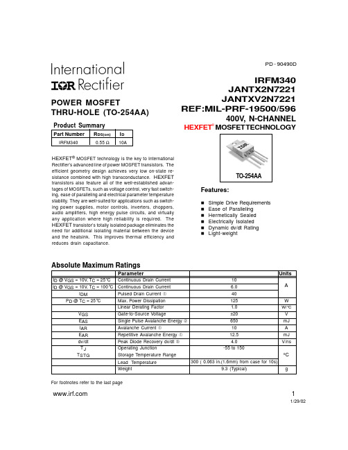
PD - 90490D
POWER MOSFET THRU-HOLE (TO-254AA)
Product Summary
Part Number RDS(on) ID
IRFM340
0.55 Ω 10A
IRFM340 JANTX2N7221 JANTXV2N7221 REF:MIL-PRF-19500/596 400V, N-CHANNEL
— 0.55 — 0.70 — 4.0 —— — 25 — 250
— 100 — -100 — 65 — 10 — 40.5 — 25 — 92 — 79 — 58 6.8 —
1400 — 350 — 230 —
Ω V S( ) µA
nA nC
ns
Ω
VGS = 10V, ID = 6.0A ➃ VGS = 10V, ID = 10A VDS = VGS, ID = 250µA VDS > 15V, IDS = 6.0A ➃ VDS= 320V ,VGS=0V
Current Regulator Same Type as D.U.T.
50KΩ
102V
.2µF
.3µF
+ D.U.T. -VDS
VGS
Input Capacitance
—
Coss
Output Capacitance
—
Crss
Reverse Transfer Capacitance
—
Typ Max Units —— V 0.49 — V/°C
Test Conditions VGS = 0V, ID = 1.0mA Reference to 25°C, ID = 1.0mA
—
JAN2N6032中文资料
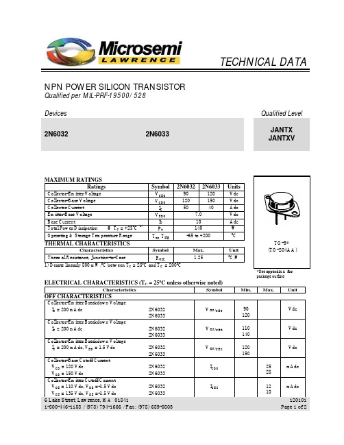
*See appendix A for package outline
ELECTRICAL CHARACTERISTICS (TC = 250C unless otherwise noted)
Characteristics Symbol Min. Max. Unit
OFF CHARACTERISTICS
2N6032 2N6033 2N6032 2N6033 2N6032 2N6033
hFE
10 10
50 50 1.3 1.0 2.0 2.0 Vdc
VCE(sat)
VBE(sat)
Vdc
DYNAMIC CHARACTERISTICS
Magnitude of Common Emitter Small-Signal Short-Circuit Forward Current Transfer Ratio IC = 2.0 Adc, VCE = 10 Vdc, f = 5.0 MHz Output Capacitance VCB = 10 Vdc, IE = 0, 100 kHz ≤ f ≤ 1.0 MHz hfe Cobo 10 40 1,000 pF
6 Lake Street, Lawrence, MA 01841 1-800-446-1158 / (978) 794-1666 / Fax: (978) 689-0803
120101 Page 2 of 2
Collector-Emitter Voltage Collector-Base Voltage Collector Current Emitter-Base Voltage Base Current Total Power Dissipation
Symbol
JAN2N3821中文资料
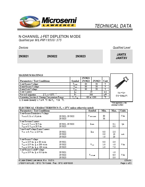
TECHNICAL DATA N-CHANNEL J-FET DEPLETION MODEQualified per MIL-PRF-19500/375Devices Qualified Level2N3821 2N3822 2N3823JANTX JANTXVMAXIMUM RATINGSParameters / Test Conditions Symbol 2N38212N3822 2N3823 UnitGate-Source Voltage V GSR50 30 V Drain-Source Voltage V DS50 30 V Drain-Gate Voltage V DG50 30 V Gate Current I GF 10 mA Power Dissipation T A = +250C (1)P T300 mW Operating Junction & Storage Temperature Range T j, T stg-55 to +200 0C(1) Derate linearly 1.7 mW/C for T A +25 C.package outline ELECTRICAL CHARACTERISTICS (T A = 250C unless otherwise noted)Parameters / Test Conditions Symbol Min. Max. Units Gate-Source Breakdown VoltageV DS = 0, I G = 1.0 µAdc 2N3821, 2N3822 2N3823 V(BR)GSSR5030VdcGate Reverse CurrentV DS = 0, V GS = 30 Vdc 2N3821, 2N3822 V DS = 0, V GS = 20 Vdc 2N3823 I GSSR0.10.5ηAZero-Gate-Voltage Drain CurrentV GS = 0, V DS = 15 Vdc 2N3821 2N3822 2N3823 I DSS0.52.04.02.51020mAGate-Source VoltageV DS = 15 Vdc, I D = 50 µAdc 2N3821V DS = 15 Vdc, I D = 200 µAdc 2N3822 V DS = 15 Vdc, I D = 400 µAdc 2N3823 V GS0.51.01.02.04.07.5VdcGate-Source Cutoff VoltageV DS = 15 Vdc, I D = 0.5 ηAdc 2N38212N3822 2N3823 V GS(off)4.06.08.0Vdc6 Lake Street, Lawrence, MA 018411-800-446-1158 / (978) 794-1666 / Fax: (978) 689-0803120101 Page 1 of 22N3821, 2N3822, 2N3823 JAN SERIESParameters / Test Conditions Symbol Min. Max. Units Small-Signal Common Source, Short-Circuit Forward Transfer AdmittanceV GS = 0, V DS = 15 Vdc, f = 1.0 kHz 2N38212N3822 2N3823 |y fs|1150030003500450065006500µSSmall-Signal Common Source, Short-Circuit Output AdmittanceV GS = 0, V DS = 15 Vdc, f = 1.0 kHz 2N38212N3822 2N3823 |y os|102035µSSmall-Signal, Common-Source Short-Circuit Input CapacitanceV GS = 0, V DS = 15 Vdc, 100 kHz ≤ f ≤ 1.0 MHz C iss 6.0 pF Small-Signal, Common-Source Reverse Transfer CapacitanceV DS = 15 Vdc, V GS = 0, 100 kHz ≤ f ≤ 1.0 MHz2N3821, 2N3822 2N3823C rss3.02.0pFSmall-Signal Common Source, Short-Circuit Forward Transfer AdmittanceV GS = 0, V DS = 15 Vdc, f = 100 MHz 2N3821f = 100 MHz 2N3822 f = 200 MHz 2N3823 |y fs|2150030003200µSSmall-Signal, Common-Source Short-Circuit Input ConductanceV GS = 0, V DS = 15 Vdc, f = 200 MHz 2N3823 (only)g is 800 µS Small-Signal, Common-Source Short-Circuit Output ConductanceV GS = 0, V DS = 15 Vdc, f = 200 MHz 2N3823 (only)g os 200 µS Common Source Spot Noise FigureV GS = 0, V DS = 15 Vdc, R G = 1MΩf = 10 Hz2N3821, 2N3822f = 1.0 kHz 2N3821, 2N3822, 2N3823NF1 5.02.0dBCommon Source Spot Noise FigureV GS = 0, V DS = 15 Vdc, R G = 1kΩf = 105 MHz2N3823 (only)NF22.5dB6 Lake Street, Lawrence, MA 018411-800-446-1158 / (978) 794-1666 / Fax: (978) 689-0803120101 Page 2 of 2。
2N5551中文资料_数据手册_参数

Packing Method Ammo
Tape and Reel Tape and Reel
Bulk Tape and Reel
© 2009 Fairchild Semiconductor Corporation
Top Mark 5551 5551 5551 5551 3S
Package TO-92 3L TO-92 3L TO-92 3L TO-92 3L SOT-23 3L
Note: 1. Suffix “-C” means Center Collector in 2N5551 (1. Emitter 2. Collector 3. Base)
Symbol
Parameter
Value
Units
VCEO VCBO VEBO
IC TJ, Tstg(2)
Collector-Emitter Voltage Collector-Base Voltage Emitter-Base Voltage Collector current - Continuous Junction and Storage Temperature
2N5551 / MMBT5551 Rev. 1.1.0
1
2N5551 / MMBT5551 — NPN General-Purpose Amplifier
Absolute Maximum Ratings(2)
Stresses exceeding the absolute maximum ratings may damage the device. The device may not function or be operable above the recommended operating conditions and stressing the parts to these levels is not recommended. In addition, extended exposure to stresses above the recommended operating conditions may affect device reliability. The absolute maximum ratings are stress ratings only. Values are at TA = 25°C unless otherwise noted.
JAN2N5661资料
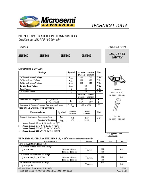
2N5660 2N5661 2N5662 2N5663 200 300 250 400 250 400 6.0 0.5 2.0 2N5660 2N5662 2N5661 2N5663 2.0(1) 1.0(2) (3) 20 15(4) -65 to +200 2N5662 2N5663 6.67 145.8
V(BR)CER V(BR)EBO
Vdc Vdc
6 Lake Street, Lawrence, MA 01841 1-800-446-1158 / (978) 794-1666 / Fax: (978) 689-0803
120101 Page 1 of 2
元器件交易网
SWITCHING CHARACTERISTICS
Turn-On Time VCC = 100 Vdc; IC = 0.5 Adc; IB1 = 15 Adc 2N5660, 2N5662 VCC = 100 Vdc; IC = 0.5 Adc; IB1 = 25 Adc 2N5661, 2N5663 Turn-Off Time VCC = 100 Vdc; IC = 0.5 Adc; IB1 = -IB2 = 15 Adc 2N5660, 2N5662 VCC = 100 Vdc; IC = 0.5 Adc; IB1 = -IB2 = 25 Adc 2N5661, 2N5663
ICBO
ON CHARACTERISTICS (5)
2N5660, 2N5662 2N5661, 2N5663 2N5660, 2N5662 2N5661, 2N5663 All Types All Types
hFE
40 25 40 25 15 5.010 75VCE(sat)
0.4 0.8 1.2 1.5
JAN2N5302中文资料
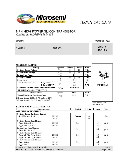
Symbol
VCEO VCBO VEBO IC IB PT TJ, Tstg Symbol RθJC
2N5302
60 60 5.0 30
2N5303
80 80
Unit
Vdc Vdc Vdc Adc Adc W W/0C 0 C Unit C/W
@ TA = +250C(1) @ TC = +1000C(2) Operating & Storage Junction Temperature Range
0
*See appendix A for package outline
ELECTRICAL CHARACTERISTICS
Characteristics Symbol Min. Max. Unit
OFF CHARACTERISTICS
Collector-Emitter Breakdown Current IC = 200 mAdc, IB = 0 Collector-Emitter Cutoff Current VCE = 60 Vdc, IB = 0 VCE = 80 Vdc, IB = 0 Emitter-Base Cutoff Current VEB = 5.0 Vdc, IC = 0 Collector-Emitter Cutoff Current VBE = 1.5 Vdc, VCE = 60 Vdc VBE = 1.5 Vdc, VCE = 80 Vdc Collector-Emitter Cutoff Current VCE = 60 Vdc VCE = 80 Vdc 2N5302 2N5303 2N5302 2N5303 V(BR)CEO 60 80 10 10 5.0 5.0 5.0 5.0 5.0 Vdc
JAN1N5611中文资料
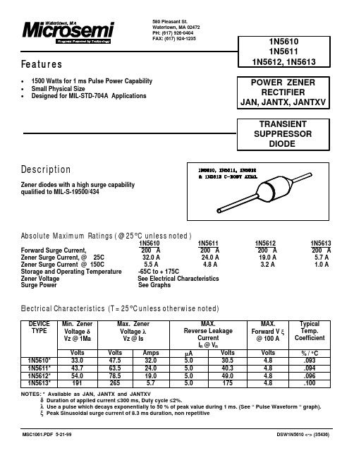
• 1500 Watts for 1 ms Pulse Power Capability • Small Physical Size• Designed for MIL-STD-704A ApplicationsDescriptionZener diodes with a high surge capability qualified to MIL-S-19500/434Absolute Maximum Ratings ( @ 25°C unless noted )1N5610 1N5611 1N5612 1N5613Forward Surge Current, 200 A 200 A 200 A 200 A Zener Surge Current, @ 25C 32.0 A 24.0 A 19.0 A 5.7 A Zener Surge Current @ 150C 5.5 A 4.8 A 3.2 A 1.0 A Storage and Operating Temperature -65C to + 175CZener Voltage See Electrical Characteristics Surge Power See GraphsElectrical Characteristics (T = 25°C unless otherwise noted)Min. Zener Voltage δVz @ 1Ma Max. Zener Voltage λVz @ Is MAX.Reverse LeakageCurrent I R @ V RMAX.Forward V ξ@ 100 ATypical Temp.Coefficient DEVICE TYPEVolts Volts Amps µAVolts Volts % / °C 1N5610*33.047.532.0 5.030.5 4.8.0931N5611*43.763.524.0 5.040.3 4.8.0941N5612*54.078.519.0 5.049.0 4.8.0961N5613*1912655.75.01754.8.100NOTES: * Available as JAN, JANTX and JANTXVδ Duration of applied current ≤300 ms, Duty cycle ≤2%.λ Use a pulse which decays exponentially to 50 % of peak value during 1 ms. (See “ Pulse Waveform “ graph). ξ Peak Sinusoidal surge current of 8.3 ms duration, non repetitivePOWER ZENER RECTIFIERJAN, JANTX, JANTXVApplicationsVoltage transients can be suppressed with series elements, shunt elements or a combination of both. These elements may be passive or active. For low & medium power applications, a series resistor & zener clamp offer several attractive features:1. Simplicity of design.2. High reliability.3. Fast response time.The 1N5610 series will suppress the following transients (defined by MIL-S-704A) without using any series limiting resistance; (except as noted in line #3 below)1. All 600 V transients (category 1 in chart below).2. All 80 V transients except those generated by the main voltage regulator (category 2 in chart below).3. Over-voltage transients from the main voltage regulator (category 3 in chart below) will be suppressed if:a. A 20 ohm series limiting resistor is used, or-b. No series resistance is used & the zener is protected within 500 µs, using (for example) an SCR crowbar.The above statements are based on the source impedances & dv/dt characteristics as given in ARINC* spec# 413; entitled “Guidance for Aircraft Electrical Power Utilization & Transient Protection. This report further defines MIL-STD-704A in regard to large aircraft electrical systems.These surge suppressors are useful in a varierty of other applications where semiconductor devices must function in an environment subject to extremely high, but short term surges.* ARINC stands for Aeronautical Radio Incorporated; Annapolis, Maryland 21401DEVICE OUTLINEDIE OUTLINEFIGURE 1FIGURE 2FIGURE 3。
JAN2N5152中文资料
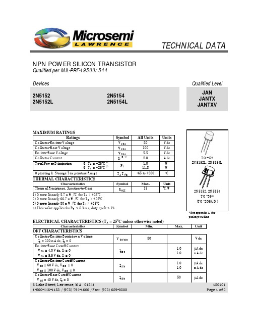
MAXIMUM RATINGS Ratings
Collector-Emitter Voltage Collector-Base Voltage Emitter-Base Voltage Collector Current Total Power Dissipation
Symbol
VCEO VCBO VEBO IC(3, 4) PT Tj, Tstg Symbol RθJC
ICES ICEO
6 Lake Street, Lawrence, MA 01841 1-800-446-1158 / (978) 794-1666 / Fax: (978) 689-0803
120101 Page 1 of 2
元器件交易网
2N5152, 2N5154 JAN SERIES ELECTRICAL CHARACTERISTICS (con’t)
VBE
Vdc
VBE(sat)
1.ห้องสมุดไป่ตู้5 2.2
Vdc
DYNAMIC CHARACTERISTICS
Magnitude of Common Emitter Small-Signal Short Circuit Forward-Current Transfer Ratio IC = 500 mAdc, VCE = 5 Vdc, f = 10 MHz 2N5152 2N5154 Small-Signal Short Circuit Forward-Current Transfer Ratio IC = 100 mAdc, VCE = 5 Vdc, f = 1 kHz 2N5152 2N5154 Output Capacitance VCB = 10 Vdc, IE = 0, f = 1.0 MHz
JANTXV1N759D中文资料

SCOTTSDALE DIVISION
DESCRIPTION The popular 1N746 thru 1N759A and 1N4370 thru 1N4372A series of 0.5 watt Zener Voltage Regulators provides a selection from 2.4 to 12 volts in standard 5% or 10% tolerances as well as tighter tolerances identified by different suffix letters on the part number. These glass axial-leaded DO-35 Zeners are also available with an internal-metallurgical-bond option by adding a “-1” suffix. These are also available in JAN, JANTX, and JANTXV military qualifications. Microsemi also offers numerous other Zener products to meet higher and lower power applications.
WWW . Microsemi .C OM
IZT
mA 20 20 20 20 20 20 20 20 20 20 20 20 20 20 20 20 20
IZM
* JEDEC Registered Data
JANTXV2N6796中文资料
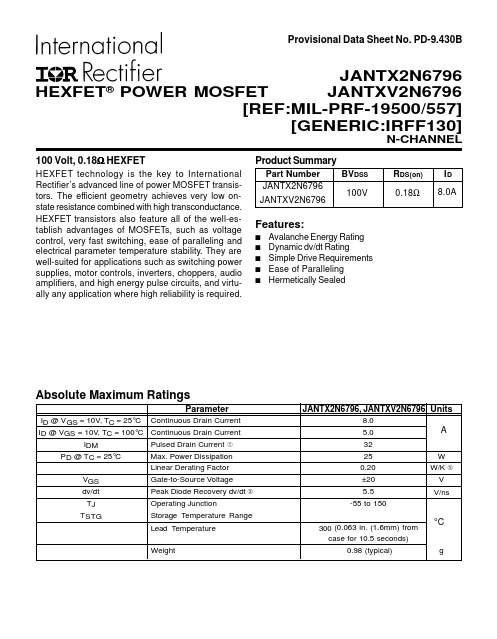
Product SummaryPart Number BV DSS R DS(on)I D JANTX2N6796JANTXV2N6796Features:s Avalanche Energy Rating s Dynamic dv/dt Ratings Simple Drive Requirements s Ease of Paralleling sHermetically SealedN-CHANNELProvisional Data Sheet No. PD-9.430B100 Volt, 0.18Ω HEXFETHEXFET technology is the key to International Rectifier’s advanced line of power MOSFET transis-tors. The efficient geometry achieves very low on-state resistance combined with high transconductance.HEXFET transistors also feature all of the well-es-tablish advantages of MOSFETs, such as voltage control, very fast switching, ease of paralleling and electrical parameter temperature stability. They are well-suited for applications such as switching power supplies, motor controls, inverters, choppers, audio amplifiers, and high energy pulse circuits, and virtu-ally any application where high reliability is required.JANTX2N6796JANTXV2N6796[REF:MIL-PRF-19500/557][GENERIC:IRFF130]HEXFET ® POWER MOSFET ParameterJANTX2N6796, JANTXV2N6796UnitsI D @ V GS = 10V, T C = 25°C Continuous Drain Current 8.0I D @ V GS = 10V , T C = 100°CContinuous Drain Current 5.0I DMPulsed Drain Current 32P D @ T C = 25°CMax. Power Dissipation 25W Linear Derating Factor 0.20W/K V GS Gate-to-Source Voltage±20V dv/dt Peak Diode Recovery dv/dt 5.5V/nsT J Operating Junction-55 to 150T STGStorage Temperature Range Lead Temperature 300(0.063 in. (1.6mm) from case for 10.5 seconds)Weight0.98 (typical)goCA8.0A0.18Ω100V元器件交易网Thermal ResistanceParameterMin.Typ.Max.UnitsTest ConditionsR thJC Junction-to-Case —— 5.0R thJAJunction-to-Ambient——175K/WTypical socket mountSource-Drain Diode Ratings and CharacteristicsParameterMin.Typ.Max.UnitsTest ConditionsI S Continuous Source Current (Body Diode)——8.0Modified MOSFET symbol showing the I SMPulse Source Current (Body Diode)——32integral reverse p-n junction rectifier.V SD Diode Forward Voltage —— 1.5V T j = 25°C, I S = 8.0A, V GS = 0V t rr Reverse Recovery Time ——300ns T j = 25°C, I F = 8.0A, di/dt ≤ 100A/µsQ RR Reverse Recovery Charge —— 3.0µCV DD ≤ 50Vt onForward Turn-On TimeIntrinsic turn-on time is negligible. Turn-on speed is substantially controlled by L S + L D .Electrical Characteristics @ Tj = 25°C (Unless Otherwise Specified)DS = 25Vf = 1.0 MHz see figure 5AFig. 1 — T ypical Output CharacteristicsT C = 25°C Fig. 2 — T ypical Output CharacteristicsT C = 150°CFig. 3 — Typical Transfer Characteristics Fig. 4 — Normalized On-Resistance Vs.TemperatureFig. 5 — T ypical Capacitance Vs. Drain-to-SourceVoltage Fig. 6 — T ypical Gate Charge Vs. Gate-to-SourceVoltageFig. 10b — Switching Time WaveformsFig. 10a — Switching Time Test Circuit Fig. 8 — Maximum Safe Operating AreaFig. 9 — Maximum Drain Current Vs. Case TemperatureFig. 7 — Typical Source-to-Drain Diode ForwardVoltageFig. 13a — Gate Charge T est CircuitFig. 12a — Unclamped Inductive T est Circuit Fig. 12b — Unclamped Inductive WaveformsFig. 11 — Maximum Effective Transient Thermal Impedance, Junction-to-Case Vs. Pulse DurationJANTX2N6796, JANTXV2N6796 DeviceCase Outline and Dimensions — TO-205AF (Modified TO-39)Repetitive Rating; Pulse width limited by maximum junction temperature.(see figure 11)@ V DD = 25V , Starting T J = 25°C,E AS = [0.5 * L * (I L 2) * [BV DSS /(BV DSS -V DD )]Peak I L = 8.0A, V GS = 10V , 25 ≤ R G ≤ 200ΩWORLD HEADQUARTERS: 233 Kansas St., El Segundo, California 90245, Tel: (310) 322 3331EUROPEAN HEADQUARTERS: Hurst Green, Oxted, Surrey RH8 9BB, UK Tel: ++ 44 1883 732020IR CANADA: 7321 Victoria Park Ave., Suite 201, Markham, Ontario L3R 2Z8, Tel: (905) 475 1897IR GERMANY: Saalburgstrasse 157, 61350 Bad Homburg Tel: ++ 49 6172 96590IR ITALY: Via Liguria 49, 10071 Borgaro, Torino Tel: ++ 39 11 451 0111IR FAR EAST: K&H Bldg., 2F, 3-30-4 Nishi-Ikeburo 3-Chome, Toshima-Ki, Tokyo Japan 171 Tel: 81 3 3983 0086IR SOUTHEAST ASIA: 315 Outram Road, #10-02 Tan Boon Liat Building, Singapore 0316 Tel: 65 221 8371/Data and specifications subject to change without notice.10/96All dimensions are shown millimeters (inches)。
半导体命名规则
半导体命名规则.txt不要放弃自己! -------(妈妈曾经这样对我说,转身出门的一刹那,我泪流满面,却不想让任何人看见!)看到这一句小编也心有感触,想起当初离家前往几千里外的地方的时候,妈妈也说过类似的话,但是身为男儿,必须创出一片天,才能报答父母的养育之恩!!中国三极管型号命名方法中国半导体器件型号由五部分(场效应器件、半导体特殊器件、复合管、PIN型管、激光器件的型号命名只有第三、四、五部分)组成。
五个部分意义如下:第一部分:用数字表示半导体器件有效电极数目。
2-二极管3-三极管第二部分:用汉语拼音字母表示半导体器件的材料和极性。
表示二极管时:A-N型锗材料B-P型锗材料C-N型硅材料D-P型硅材料表示三极管时:A-PNP型锗材料、B-NPN型锗材料、C-PNP型硅材料、D-NPN型硅材料。
第三部分:用汉语拼音字母表示半导体器件的类型。
P-普通管、V-微波管W-稳压管C-参量管Z-整流管L-整流堆S-隧道管N-阻尼管U-光电器件K-开关管X-低频小功率管(F<3MHz,Pc<1W)G-高频小功率管(f>3MHz,Pc<1W)D -低频大功率管(f<3MHz,Pc>1W)A-高频大功率管(f>3MHz,Pc>1W)T-半导体晶闸管(可控整流器)Y-体效应器件B-雪崩管J-阶跃恢复管CS-场效应管BT-半导体特殊器件FH-复合管PIN-PIN型管JG-激光器件。
第四部分:用数字表示序号第五部分:用汉语拼音字母表示规格号例如:3DG18表示NPN型硅材料高频三极管美国三极管型号命名方法美国晶体管或其他半导体器件的命名法较混乱。
美国电子工业协会半导体分立器件命名方法如下:1.第一部分:用符号表示器件用途的类型。
JAN-军级JANTX-特军级JANTXV-超特军级JANS-宇航级(无)-非军用品。
2.第二部分:用数字表示pn结数目。
1-二极管2-三极管3-三个pn结器件n-依次类推3.第三部分:美国电子工业协会(EIA)注册标志。
JAN1N5711UR-1中文资料
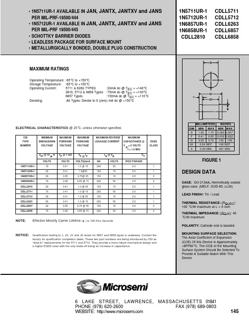
100,000
10,000
1000
1
10
1 0 10 20 30 40 50 60 VR – REVERSE VOLTAGE (V) (PULSED) Figure 4. CDLL5711 Typical Variation of Reverse Current (IR) vs. Reverse Voltage (VR) at Various Temperatures.
POLARITY: Cathode end is banded.
MOUNTING SURFACE SELECTION: The Axial Coefficient of Expansion (COE) Of this Device is Approximately +6PPM/°C. The COE of the Mounting Surface System Should Be Selected To Provide A Suitable Match With This Device.
1N5711UR-1 1N5712UR-1 1N6857UR-1 1N6858UR-1 CDLL2810
CDLL5711 CDLL5712 CDLL6263 CDLL6857 CDLL6858
MAXIMUM RATINGS
Operating Temperature: -65°C to +150°C
Storage Temperature: -65°C to +150°C
6 LAKE STREET, LAWRENCE, MASSACHUSETTS 01841
PHONE (978) 620-2600
FAX (978) 689-0803
WEBSITE:
JAN2N3822中文资料

TECHNICAL DATA N-CHANNEL J-FET DEPLETION MODEQualified per MIL-PRF-19500/375Devices Qualified Level2N3821 2N3822 2N3823JANTX JANTXVMAXIMUM RATINGSParameters / Test Conditions Symbol 2N38212N3822 2N3823 UnitGate-Source Voltage V GSR50 30 V Drain-Source Voltage V DS50 30 V Drain-Gate Voltage V DG50 30 V Gate Current I GF 10 mA Power Dissipation T A = +250C (1)P T300 mW Operating Junction & Storage Temperature Range T j, T stg-55 to +200 0C(1) Derate linearly 1.7 mW/C for T A +25 C.package outline ELECTRICAL CHARACTERISTICS (T A = 250C unless otherwise noted)Parameters / Test Conditions Symbol Min. Max. Units Gate-Source Breakdown VoltageV DS = 0, I G = 1.0 µAdc 2N3821, 2N3822 2N3823 V(BR)GSSR5030VdcGate Reverse CurrentV DS = 0, V GS = 30 Vdc 2N3821, 2N3822 V DS = 0, V GS = 20 Vdc 2N3823 I GSSR0.10.5ηAZero-Gate-Voltage Drain CurrentV GS = 0, V DS = 15 Vdc 2N3821 2N3822 2N3823 I DSS0.52.04.02.51020mAGate-Source VoltageV DS = 15 Vdc, I D = 50 µAdc 2N3821V DS = 15 Vdc, I D = 200 µAdc 2N3822 V DS = 15 Vdc, I D = 400 µAdc 2N3823 V GS0.51.01.02.04.07.5VdcGate-Source Cutoff VoltageV DS = 15 Vdc, I D = 0.5 ηAdc 2N38212N3822 2N3823 V GS(off)4.06.08.0Vdc6 Lake Street, Lawrence, MA 018411-800-446-1158 / (978) 794-1666 / Fax: (978) 689-0803120101 Page 1 of 22N3821, 2N3822, 2N3823 JAN SERIESParameters / Test Conditions Symbol Min. Max. Units Small-Signal Common Source, Short-Circuit Forward Transfer AdmittanceV GS = 0, V DS = 15 Vdc, f = 1.0 kHz 2N38212N3822 2N3823 |y fs|1150030003500450065006500µSSmall-Signal Common Source, Short-Circuit Output AdmittanceV GS = 0, V DS = 15 Vdc, f = 1.0 kHz 2N38212N3822 2N3823 |y os|102035µSSmall-Signal, Common-Source Short-Circuit Input CapacitanceV GS = 0, V DS = 15 Vdc, 100 kHz ≤ f ≤ 1.0 MHz C iss 6.0 pF Small-Signal, Common-Source Reverse Transfer CapacitanceV DS = 15 Vdc, V GS = 0, 100 kHz ≤ f ≤ 1.0 MHz2N3821, 2N3822 2N3823C rss3.02.0pFSmall-Signal Common Source, Short-Circuit Forward Transfer AdmittanceV GS = 0, V DS = 15 Vdc, f = 100 MHz 2N3821f = 100 MHz 2N3822 f = 200 MHz 2N3823 |y fs|2150030003200µSSmall-Signal, Common-Source Short-Circuit Input ConductanceV GS = 0, V DS = 15 Vdc, f = 200 MHz 2N3823 (only)g is 800 µS Small-Signal, Common-Source Short-Circuit Output ConductanceV GS = 0, V DS = 15 Vdc, f = 200 MHz 2N3823 (only)g os 200 µS Common Source Spot Noise FigureV GS = 0, V DS = 15 Vdc, R G = 1MΩf = 10 Hz2N3821, 2N3822f = 1.0 kHz 2N3821, 2N3822, 2N3823NF1 5.02.0dBCommon Source Spot Noise FigureV GS = 0, V DS = 15 Vdc, R G = 1kΩf = 105 MHz2N3823 (only)NF22.5dB6 Lake Street, Lawrence, MA 018411-800-446-1158 / (978) 794-1666 / Fax: (978) 689-0803120101 Page 2 of 2。
JAN2N1131资料
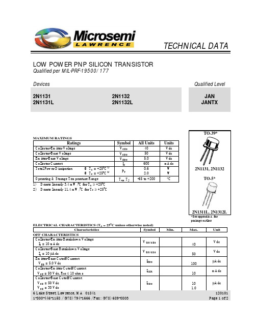
TECHNICAL DATA
LOW POWER PNP SILICON TRANSISTOR
Qualified per MIL-PRF-19500/177 Devices 2N1131 2N1131L 2N1132 2N1132L Qualified Level JAN JANTX
All Units
40 50 5.0 600 0.6 2.0 -65 to +200
Units
Vdc Vdc Vdc mAdc W W °C
@ TA = +250C(1) @ TC = +250C(2) Operating & Storage Temperature Range 1) Derate linearly 3.4 mW/0C for TA ≥ +250C 2) Derate linearly 11.4 mW/0C for TC ≥ +250C
Min.
Max.
Unit Vdc Vdc µAdc mAdc µAdc
40 50 100 10 10 1.0
6 Lake Street, Lawrence, MA 01841 1-800-446-1158 / (978) 794-1666 / Fax: (978) 689-0803
ห้องสมุดไป่ตู้
120101 Page 1 of 2
TO-39*
MAXIMUM RATINGS
Ratings
Collector-Emitter Voltage Collector-Base Voltage Emitter-Base Voltage Collector Current Total Power Dissipation
- 1、下载文档前请自行甄别文档内容的完整性,平台不提供额外的编辑、内容补充、找答案等附加服务。
- 2、"仅部分预览"的文档,不可在线预览部分如存在完整性等问题,可反馈申请退款(可完整预览的文档不适用该条件!)。
- 3、如文档侵犯您的权益,请联系客服反馈,我们会尽快为您处理(人工客服工作时间:9:00-18:30)。
25 25 10
mAdc mAdc
ON CHARACTERISTICS
Forward-Current Transfer Ratio IC = 15 Adc, VCE = 2.0 Vdc IC = 20 Adc, VCE = 5.0 Vdc Collector-Emitter Saturation Voltage IC = 15 Adc, IB = 1.2 Adc IC = 30 Adc, IB = 6.0Adc Base-Emitter Saturation Voltage IC = 15 Adc, IB = 1.2 Adc
元器件交易网
2N5671, 2N5672 JAN SERIES
ELECTRICAL CHARACTERISTICS (con’t)
Characteristics Symbol Min. Max. Unit
OFF CHARACTERISTICS (con’t)
Collector-Base Cutoff Current VCB = 120 Vdc VCB = 150 Vdc Emitter-Base Cutoff Current VEB = 7.0 Vdc 2N5671 2N5672 ICBO IEBO
VCEO VCBO VEBO IB IC PT Top, Tstg Symbol RθJC
2N5671
90 120
2N5672
120 150
Unit
Vdc Vdc Vdc Adc Adc W W 0 C Unit C/W
@ TA = +250C (1) @ TC = +250C (2) Operating & Storage Temperature Range
OFF CHARACTERISTICS
Collector-Emitter Breakdown Voltage IC = 200 mAdc Collector-Emitter Breakdown Voltage IC = 200 mAdc Collector-Emitter Breakdown Voltage IC = 200 mAdc Collector-Emitter Cutoff Current VCE = 80 Vdc Collector-Emitter Cutoff Current VCE = 110 Vdc, VBE = 1.5 Vdc VCE = 135 Vdc, VBE = 1.5 Vdc 2N5671 2N5672 2N5671 2N5672 2N5671 2N5672 V(BR)CEO 90 120 110 140 120 150 10 12 10 Vdc
6 Lake Street, Lawrence, MA 01841 1-800-446-1158 / (978) 794-1666 / Fax: (978) 689-0803
120101 Page 2 of 2
t
off
SAFE OPERATING AREA
DC Tests TC = +250C, 1 Cycle, t = 1.0 s Test VCE = 24 Vdc, IC = 5.8 Adc Test 2 VCE = 45 Vdc, IC = 0.9 Adc Test 3 VCE = 4.67 Vdc, IC = 30 Adc Test 4 VCE = 90 Vdc, IC = 0.19 Adc 2N5671 Test 5 VCE = 120 Vdc, IC = 0.11 Adc 2N5672 (3) Pulse Test: Pulse Width = 300µs, Duty Cycle ≤ 2.0%.
7.0 10 30 6.0 140 -65 to +200 Max. 1.25
THERMAL CHARACTERISTICS
Characteristics Thermal Resistance, Junction-to-Case 1) Derate linearly 34.2 mW/0C for TA > +250C 2) Derate linearly 800 mW/0C for TC > +250C
t
10
40 900 pF
SWITCHING CHARACTERISTICS
Turn-On Time VCC = 30 ± 2.0 Vdc; IC = 15 Adc; IB1 = 1.2 Adc Turn-Off Time VCC = 30 ± 2.0 Vdc; IC = 15 Adc; IB1 = IB2 = 1.2 Adc on 0.5 1.5 µs µs
V(BR)CER
Vdc
V(BR)CEX ICEO
Vdc mAdc mAdc
2N5671 2N5672
ICEX
6 Lake Street, Lawrence, MA 01841 1-800-446-1158 / (978) 794-1666 / Fax: (978) 689-0803
120101 Page 1 of 2
MAXIMUM RATINGS Ratings
Collector-Emitter Voltage Collector-Base Voltage Emitter-Base Voltage Base Current Collector Current Total Power Dissipation
Symbol
元器件交易网
TECHNICAL DATA
NPN HIGH POWER SILICON TRANSISTOR
Qualified per MIL-PRF-19500/488 Devices 2N5671 2N5672 Qualified Level JAN JANTX JANTXV
0
TO-3* (TO-204AA)
*See appendix A for package outlin50C unless otherwise noted)
Characteristics Symbol Min. Max. Unit
hFE
20 20
100
VCE(sat) VBE(sat)
0.75 5.0 1.5
Vdc Vdc
DYNAMIC CHARACTERISTICS
Magnitude of Common Emitter Small-Signal Short-Circuit Forward Current Transfer Ratio IC = 2.0 Adc, VCE = 10 Vdc, f = 5.0 MHz Output Capacitance VCB = 10 Vdc, IE = 0, 100 kHz ≤ f ≤ 1.0 MHz hfe Cobo