wm8731驱动源码
WM8731的应用
WM8731的应用WM8731作为一个低功耗立体声的编码解码器和一个集成的耳机驱动。
它提供一个独特的能力对于可编程的AD和DA采样速率从一个时钟源。
、WM8731对于外接DSP或者FPGA作为音频数据处理时,其通过5线连接,bclk为bit 时钟的控制,DACLRC/ADCLRC为其数据采集速率,DACDAT和ADCDAT为数字和模拟端,通过AD出来的数据进入FPGA中进行进行处理,通过FPGA处理过后的数据输出DA 内。
对于其寄存器的一共有十六个寄存器,每个寄存器有16位,高七位为地址,低九位为数据。
R0(00):其中低五位为输入左声道增益控制端,第七位左声道输入使能端,第八位左右声道是否同时载入及其增益。
R2(02):同RO,右声道。
R3(04):第六位为左声道耳机输出端增益控制端,第七位为左通道零交叉检测启用,第八位左右耳机输出声道是否同时载入及其增益。
R4(06):同R3,右声道。
R5(08):最低位为麦克风增益加强,第一位为麦克风使能输入ADC使能,第二位为麦克风输入还是输入线输入,第三位为旁路开关选择,第四位为DA使能,第五位为音调选择开关,第六,七位为音调的衰减。
R6(0A):最低位为ADC高通滤波器使能,2,1位为DE加强控制,3位为DA软件沉默使能,R7(0C):0位为线性输入功率下降,1位为麦克风输入和偏执功率下降,2位为AD功率下降,3位为DA功率下降,4位为输入功率下降,5位为振荡器功率下降,6位为输出功率下降,7位为电源使能。
R8(0E):1,0位为数据输出模型选择,3,2位为输出数据bit位数的选择,4位为输出数据相移的选择,5位为DA左右声道的时钟交换选择,6位为从设备模型控制,7位为bit时钟嵌入选择R9(10):0位为USB或者正常模型,1为基础过采速率,5:2为DA和AD的采样速率,6为主时钟分频选择,7为对分频时钟是否继续分频R10(12):0位为接口使能R15(1E):8:0为清零寄存器通过两线的I2C协议进行寄存器的初始化,通过麦克风或者其他输入进行直接音频输入,通过对其音频的处理,通过音频的输出。
Wm8731 音量调节程序
Wm8731 I2C控制模块module x(clock_50m,i2c_sclk,i2c_sdat,reset_n,ack,tr_end,start,config_step,reg_index,key1,i2c_data,reg2_data,clock_20k,hex1,hex2,xs1,xs2);input clock_50m;input reset_n,key1;output i2c_sclk,ack,tr_end,start,clock_20k;output[1:0] config_step;output[3:0] reg_index;output[23:0]i2c_data;output[15:0] reg2_data; //输出声道output[6:0] hex1,hex2; //七段码显示output[2:0] xs1; //LED显示output[3:0] xs2;reg[6:0] hex1,hex2;inout i2c_sdat;reg clock_20k;reg [15:0]clock_20k_cnt;reg [1:0]config_step;reg [3:0]reg_index;reg [23:0]i2c_data;reg [15:0]reg_data;reg start,bz,bx;reg[15:0] reg2_data;wire ack;wire tr_end;wire[2:0] xs1;wire[3:0] xs2;i2c u1(.clock_i2c(clock_20k),.reset_n(reset_n),.ack(ack),.i2c_data(i2c_data),.start(start),.tr_end(tr_end),.i2c_sclk(i2c_sclk),.i2c_sdat(i2c_sdat));assign {xs1,xs2}=reg2_data[6:0];always@(posedge clock_50m or negedge reset_n) //产生i2c控制时钟-20khzbeginif(!reset_n)beginclock_20k<=0;clock_20k_cnt<=0;endelse if(clock_20k_cnt<2499)clock_20k_cnt<=clock_20k_cnt+1;elsebeginclock_20k<=!clock_20k;clock_20k_cnt<=0;endendalways@(posedge clock_20k or negedge reset_n) //配置过程控制if(!reset_n)beginconfig_step<=0;start<=0;reg_index<=0;reg2_data<=16'h054d;bz<=1'b0;bx<=1'b1;endelse if(!key1)beginif(bx==1)beginbx<=0;config_step<=0;start<=0;reg_index<=0;beginif(bz==0)beginif(reg2_data[6:0]==7'b1111111)bz<=1'b1;elsereg2_data[6:0]<=reg2_data[6:0]+5;endelse if(bz==1)beginif(reg2_data[6:0]<=7'b0101111)bz<=1'b0;elsereg2_data[6:0]<=reg2_data[6:0]-5;endendendendelse if(clock_20k)beginif(key1==1)bx<=1'b1;if(reg_index<10)begincase(config_step)0:begini2c_data<={8'h34,reg_data};start<=1;config_step<=1;end1:if(tr_end)beginif(!ack)beginconfig_step<=2;start<=0;endelsebeginconfig_step<=0;start<=0;endend2:beginreg_index<=reg_index+1;config_step<=0;endendcaseendendalways@(reg_index)begincase(reg_index)0:reg_data<=16'h001f;1:reg_data<=16'h021f;2:reg_data<=16'h067f;3:reg_data<=reg2_data;4:reg_data<=16'h08c8;5:reg_data<=16'h0a06;6:reg_data<=16'h0c00;7:reg_data<=16'h0e01;8:reg_data<=16'h1002;9:reg_data<=16'h1201;default:reg_data<=16'h001a;endcaseendalways@(xs1 or xs2)begincase(xs1)3'b000: hex1= 7'b100_0000; //03'b001: hex1= 7'b111_1001; //13'b010: hex1= 7'b010_0100; //23'b011: hex1= 7'b011_0000; //33'b100: hex1= 7'b001_1001; //43'b101: hex1= 7'b001_0010; //53'b110: hex1= 7'b000_0010; //63'b111: hex1= 7'b111_1000; //7default: hex1= 7'b111_1111; //default endcasecase(xs2)4'b0000: hex2= 7'b100_0000; //04'b0001: hex2= 7'b111_1001; //14'b0010: hex2= 7'b010_0100; //24'b0011: hex2= 7'b011_0000; //34'b0100: hex2= 7'b001_1001; //44'b0101: hex2= 7'b001_0010; //54'b0110: hex2= 7'b000_0010; //64'b0111: hex2= 7'b111_1000; //74'b1000: hex2= 7'b000_0000; //84'b1001: hex2= 7'b001_1000; //94'b1010: hex2= 7'b000_1000; //A4'b1011: hex2= 7'b000_0011; //B4'b1100: hex2= 7'b100_0110; //C4'b1101: hex2= 7'b010_0001; //D4'b1110: hex2= 7'b000_0110; //E4'b1111: hex2= 7'b000_1110; //Fdefault: hex2= 7'b111_1111; //defaultendcaseendendmoduleI2C控制字(例化模块)module i2c(clock_i2c, //wm8731控制接口传输所需时钟,0-400khz,此处为20khz reset_n,ack, //应答信号i2c_data, //sdin接口传输的24位数据start, //开始传输标志tr_end, //传输结束标志cyc_count,i2c_sclk, //FPGA与wm8731时钟接口i2c_sdat); //FPGA与wm8731数据接口input [23:0]i2c_data;input reset_n;input clock_i2c;output [5:0]cyc_count;output ack;input start;output tr_end;output i2c_sclk;inout i2c_sdat;reg [5:0] cyc_count;reg reg_sdat;reg sclk;reg ack1,ack2,ack3;reg tr_end;wire i2c_sclk;wire i2c_sdat;wire ack;assign ack=ack1|ack2|ack3;assign i2c_sclk=sclk|(((cyc_count>=4)&(cyc_count<=30))?~clock_i2c:0); assign i2c_sdat=reg_sdat?1'bz:0;always@(posedge clock_i2c or negedge reset_n)beginif(!reset_n)cyc_count<=6'b111111;else beginif(start==0)cyc_count<=0;else if(cyc_count<6'b111111)cyc_count<=cyc_count+1;endendalways@(posedge clock_i2c or negedge reset_n)beginif(!reset_n)begintr_end<=0;ack1<=1;ack2<=1;ack3<=1;sclk<=1;reg_sdat<=1;endelsecase(cyc_count)0:begin ack1<=1;ack2<=1;ack3<=1;tr_end<=0;sclk<=1;reg_sdat<=1;end 1:reg_sdat<=0; //开始传输2:sclk<=0;3:reg_sdat<=i2c_data[23];4:reg_sdat<=i2c_data[22];5:reg_sdat<=i2c_data[21];6:reg_sdat<=i2c_data[20];7:reg_sdat<=i2c_data[19];8:reg_sdat<=i2c_data[18];9:reg_sdat<=i2c_data[17];10:reg_sdat<=i2c_data[16];11:reg_sdat<=1; //应答信号12:begin reg_sdat<=i2c_data[15];ack1<=0;end13:reg_sdat<=i2c_data[14];14:reg_sdat<=i2c_data[13];15:reg_sdat<=i2c_data[12];16:reg_sdat<=i2c_data[11];17:reg_sdat<=i2c_data[10];18:reg_sdat<=i2c_data[9];19:reg_sdat<=i2c_data[8];20:reg_sdat<=1; //应答信号21:begin reg_sdat<=i2c_data[7];ack2<=0;end22:reg_sdat<=i2c_data[6];23:reg_sdat<=i2c_data[5];24:reg_sdat<=i2c_data[4];25:reg_sdat<=i2c_data[3];26:reg_sdat<=i2c_data[2];27:reg_sdat<=i2c_data[1];28:reg_sdat<=i2c_data[0];29:reg_sdat<=1; //应答信号30:begin ack3<=0;sclk<=0;reg_sdat<=0;end31:sclk<=1;32:begin reg_sdat<=1;tr_end<=1;endendcaseendendmodule。
WTY-871技术及使用说明书 V1.01
3
装置功能 .......................................................................................................................................................................... 6 3.1 FC 回路保护(厂用变、电动机保护配置) ........................................................................................................ 6 3.2 (低压闭锁)过流保护(线路保护配置) .......................................................................................................... 6 3.3 复压闭锁过流保护(厂用变保护配置) .............................................................................................................. 6 3.4 过流保护(电容器、电动机保护配置) .............................................................................................................. 7 3.5 反时限过流保护(线路、厂用变、电容器、电动机保护配置) .........................................................
M88DS3103_Driver_Manual_V00_20110317_new
Montage Technology Confidential and Proprietary
iii
M88DS3103
Driver User’s Manual
1
Introduction
Montage provides a primary reference for the driver of DVB-S/S2 digital satellite demodulator M88DS3103. The driver includes a series of APIs. It can be easily integrated into the users’ applications. Users can use it as a reference, and write their own code according to the specific hardware, operating system and compiler.
INFORMATION IN THIS DOCUMENT IS PROVIDED IN CONNECTION WITH MONTAGE PRODUCTS. NO LICENSE, EXPRESS OR IMPLIED, BY ESTOPPEL OR OTHERWISE, TO ANY INTELLECTUAL PROPERTY RIGHTS IS GRANTED BY THIS DOCUMENT. EXCEPT AS PROVIDED IN MONTAGE'S TERMS AND CONDITIONS OF SALE FOR SUCH PRODUCTS, MONTAGE ASSUMES NO LIABILITY WHATSOEVER, AND MONTAGE DISCLAIMS ANY EXPRESS OR IMPLIED WARRANTY, RELATING TO SALE AND/OR USE OF MONTAGE PRODUCTS INCLUDING LIABILITY OR WARRANTIES RELATING TO FITNESS FOR A PARTICULAR PURPOSE, MERCHANTABILITY, OR INFRINGEMENT OF ANY PATENT, COPYRIGHT OR OTHER INTELLECTUAL PROPERTY RIGHT. Montage may make changes to specifications and product descriptions at any time, without notice. Designers must not rely on the absence or characteristics of any features or instructions marked "reserved" or "undefined." Montage reserves these for future definition and shall have no responsibility whatsoever for conflicts or incompatibilities arising from future changes to them. Other names and brands may be claimed as the property of others. Do not disclose or distribute to any third party without written permission of Montage. Copyright © Montage Technology 2011.
WM8734EDS中文资料
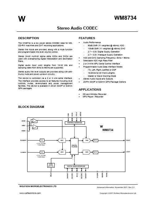
wWM8734Stereo Audio CODECWOLFSON MICROELECTRONICS LTD Advanced Information, November 2001, Rev 2.2Copyright 2001 Wolfson Microelectronics Ltd .DESCRIPTIONThe WM8734 is a low power stereo CODEC ideal for MD, CD-RW machines and DAT recording applications.Stereo line inputs are provided, along with a mute function and programmable line level volume control.Stereo 24-bit multi-bit sigma delta ADCs and DACs are used with oversampling digital interpolation and decimation filters.Digital audio input word lengths from 16-32 bits and sampling rates from 8kHz to 96kHz are supported.Stereo audio line level outputs are provided along with anti-thump mute and power up/down circuitry.The device is controlled via a 2 or 3 wire serial interface. The interface provides access to all features including level controls, mutes, de-emphasis and power management facilities. The device is available in 20-pin SSOP or 5x5mm QFN packages.FEATURES•Audio Performance− 90dB SNR (‘A’ weighted @ 48kHz) ADC − 100dB SNR (‘A’ weighted @ 48kHz) DAC − 2.7 – 3.6V Digital Supply Operation − 2.7 – 3.6V Analogue Supply Operation• ADC and DAC Sampling Frequency: 8kHz – 96kHz • Selectable ADC High Pass Filter• 2 or 3-Wire MPU Serial Control Interface •Programmable Audio Data Interface Modes − I 2S, Left, Right Justified or DSP − 16/20/24/32 bit Word Lengths − Master or Slave Clocking Mode • Stereo Audio Inputs and Outputs• 20-Pin SSOP or 5x5mm QFN Package OptionsAPPLICATIONS• CD and Minidisc Recorder • MP3 Player / RecorderBLOCK DIAGRAMC S BS D I NS C L KROUTLOUTRLINEINLLINEINVMIDD B V D D G N AVDDAGNDD C V D A D C L R CD A C L R CB C L KD A C D A TA D C D A TM C L M O D EPIN CONFIGURATION – SSOP ORDERING INFORMATION - SSOPDEVICE TEMP.RANGE PACKAGEXWM8734EDS -10to+70o C 20-pin SSOPAGNDVMIDRLINEINMCLKLLINEINMODECSBSDINSCLKDCVDDBCLKDACDATDBVDDDGNDADCDATLOUTDACLRCADCLRCROUTAVDDPIN DESCRIPTION - SSOPPIN NAME TYPE DESCRIPTION1 DGND Ground Digital GND2 DBVDD Supply Digital Buffers VDD3 BCLKDigitalInput/OutputDigital Audio Bit Clock, Pull Down, (see Note 1)4 DACDAT DigitalInput DAC Digital Audio Data Input5 DACLRCDigitalInput/OutputDAC Sample Rate Left/Right Clock. Pull Down (see Note 1)6 ADCDAT DigitalOutputADC Digital Audio Data Output7 ADCLRCDigitalInput/OutputADC Sample Rate Left/Right Clock, Pull Down (see Note 1)8 LOUTAnalogueOutputLeft Channel Line Output9 ROUTAnalogueOutputRight Channel Line Output10 AVDD Supply Analogue VDD11 AGND Ground Analogue GND12 VMID AnalogueOutputMid-rail reference decoupling point13 RLINEIN AnalogueInputRight Channel Line Input (AC coupled)14 LLINEIN AnalogueInputLeft Channel Line Input (AC coupled)15 MODE DigitalInputControl Interface Selection, Pull Up (see Note 1)16 CSB DigitalInput3-Wire MPU Chip Select / 2-Wire MPU interface address selection, active low,Pull up (see Note 1)17 SDINDigitalInput/Output3-Wire MPU Data Input / 2-Wire MPU Data Input18 SCLK DigitalInput3-Wire MPU Clock Input / 2-Wire MPU Clock Input19 MCLK DigitalInputMaster Clock Input (MCLK)20 DCVDD Supply Digital Core VDDNote:1. Pull Up/Down only present when Control Register Interface ACTIVE = 0 to conserve power.w AI Rev 2.2 November 20012PIN CONFIGURATION – QFN ORDERING INFORMATION - QFNDEVICE TEMP.RANGE PACKAGEXWM8734EFL -10to+70o C28-pin QFN(5x5x0.9mm)NCNCNCADCLRCADCDATDACLRCDACDATMCLKNCDCVDDDGNDDBVDDNCBCLKNCRLINEINLLINEINMODECSBSDINSCLKNCVMIDAGNDAVDDROUTLOUTNCPIN DESCRIPTION - QFNPIN NAME TYPE DESCRIPTION1 MCLK DigitalInputMaster Clock Input (MCLK)2 NCDoNotConnectTest Pin, must be left unconnected3 DCVDD Supply Digital Core VDD4 DGND Ground Digital GND5 DBVDD Supply Digital Buffers VDD6 NCDoNotConnectTest Pin, must be left unconnected7 BCLKDigitalInput/OutputDigital Audio Bit Clock, Pull Down, (see Note 1)8 DACDAT DigitalInput DAC Digital Audio Data Input9 DACLRCDigitalInput/OutputDAC Sample Rate Left/Right Clock. Pull Down (see Note 1)10 ADCDAT DigitalOutput ADC Digital Audio Data Output11 ADCLRCDigitalInput/OutputADC Sample Rate Left/Right Clock, Pull Down (see Note 1)12 NC DoNotConnectTest Pin, must be left unconnected13 NC DoNotConnectTest Pin, must be left unconnected14 NC DoNotConnectTest Pin, must be left unconnected15 NC DoNotConnectTest Pin, must be left unconnected16 LOUT AnalogueOutputLeft Channel Line Output17 ROUT AnalogueOutputRight Channel Line Output18 AVDD Supply Analogue VDD19 AGND Ground Analogue GND20 VMID AnalogueOutputMid-rail reference decoupling point21 NC DoNotConnectTest Pin, must be left unconnected22 NC DoNotConnectTest Pin, must be left unconnected23 RLINEIN AnalogueInputRight Channel Line Input (AC coupled)24 LLINEIN AnalogueInputLeft Channel Line Input (AC coupled)25 MODE DigitalInputControl Interface Selection, Pull Up (see Note 1)26 CSB DigitalInput3-Wire MPU Chip Select / 2-Wire MPU interface address selection, active low,Pull up (see Note 1)27 SDINDigitalInput/Output3-Wire MPU Data Input / 2-Wire MPU Data Input28 SCLK DigitalInput3-Wire MPU Clock Input / 2-Wire MPU Clock Inputw AI Rev 2.2 November 20013wAI Rev 2.2 November 20014ABSOLUTE MAXIMUM RATINGSAbsolute Maximum Ratings are stress ratings only. Permanent damage to the device may be caused by continuously operating at or beyond these limits. Device functional operating limits and guaranteed performance specifications are given under ElectricalCharacteristics at the test conditions specified.ESD Sensitive Device. This device is manufactured on a CMOS process. It is therefore generically susceptible to damage from excessive static voltages. Proper ESD precautions must be taken during handling and storage of this device.CONDITIONMIN MAX Digital supply voltage -0.3V +3.63V Analogue supply voltage -0.3V +3.63V Voltage range digital inputs DGND -0.3V DVDD +0.3V Voltage range analogue inputs AGND -0.3VAVDD +0.3VMaster Clock Frequency (see Note 4) 40MHz Operating temperature range, T A -10°C +70°CStorage temperature prior to soldering 30°C max / 85% RH max Storage temperature after soldering-65°C +150°C Package body temperature (soldering 10 seconds) +240°C Package body temperature (soldering 2 minutes) +183°CNotes: 1. Analogue and digital grounds must always be within 0.3V of each other.2. The digital supply core voltage (DCVDD) must always be less than or equal to the analogue supply voltage (AVDD) or digital supply buffer voltage (DBVDD).3. The digital supply buffer voltage (DBVDD) must always be less than or equal to the analogue supply voltage (AVDD).4. When CLKIDIV2=1.RECOMMENDED OPERATING CONDITIONSPARAMETERSYMBOLTEST CONDITIONSMIN TYP MAX UNITDigital supply range (Core) DCVDD 2.7 3.3 3.6 V Digital supply range (Buffer) DBVDD 2.7 3.3 3.6 V Analogue supply range AVDD 2.7 3.3 3.6 V GroundDGND, AGNDVTotal analogue supply current IAVDD DCVDD, DBVDD, AVDD = 3.3V 16 mADigital supply currentIDCVDD, IDBVDDDCVDD, DBVDD AVDD = 3.3V8 mAStandby Current Consumption 5 uAELECTRICAL CHARACTERISTICSTest ConditionsAVDD, DBVDD = 3.3V, AGND = 0V, DCVDD = 3.3V, DGND = 0V, T A = +25o C, Slave Mode, fs = 48kHz, MCLK = 256fs unlessotherwise stated.PARAMETER SYMBOLTESTCONDITIONSMINTYPMAXUNIT Digital Logic Levels (CMOS Levels)Input LOW level V IL0.3 x DBVDD VInput HIGH level V IH0.7 x DBVDD VOutput LOW V OL0.10xDBVDDVOutput HIGH V OH0.9 x DBVDD VPower On Reset Threshold (DCVDD)DCVDD Threshold On -> Off V th 0.9 VHysteresis V IH 0.3 VDCVDD Threshold Off -> On V OL 0.6 VAnalogue Reference LevelsReference voltage V VMID AVDD/2 V Potential divider resistance R VMID50k Ohms Line Input to ADCInput Signal Level (0dB) V INLINE 1.0AVDD/3.3VrmsSNR (Note 1,3) A-weighted, 0dB gain@ fs = 48kHz85 90 dBSNR (Note 1,3) A-weighted, 0dB gain@ fs = 96kHz90 dBSNR (Note 1,3) A-weighted, 0dB gain@ fs = 48KHz, AVDD =2.7V88 dBDynamic Range (Note 3) DNR A-weighted, -60dB fullscale input85 90 dBTHD-1dB input, 0dB gain -84 -74 dBPower Supply Rejection Ratio PSSR 1kHz100mVpp 50 dB20Hz to 20kHz100mVpp45 dBADC channel separation 1kHz input 90 dBProgrammable Gain Maximum Programmable Gain Minimum1kHz inputRsource < 50 Ohms+12-34.5dBProgrammable Gain Step Size GuaranteedMonotonic 1.5 dBMute attenuation 0dB, 1kHz input 80 dB0dB gain 20k 30k OhmsInput Resistance R INLINE12dB gain 10k 15k OhmsInput Capacitance C INLINE10 pFw AI Rev 2.2 November 20015Test ConditionsAVDD, DBVDD = 3.3V, AGND = 0V, DCVDD = 3.3V, DGND = 0V, T A = +25o C, Slave Mode, fs = 48kHz, MCLK = 256fs unlessotherwise stated.TYPMAXUNITMINPARAMETER SYMBOLTESTCONDITIONSLine Output for DAC Playback Only (Load= 47k ohms. 50pF)0dBfs Full scale output voltage At LINE outputs 1.0 xVrmsAVDD/3.3SNR (Note 1,2,3) A-weighted,90 100 dB@ fs = 48kHzSNR (Note 1,2,3) A-weighted98 dB@ fs = 96kHzSNR (Note 1,2,3) A-weighted,93 dB@ fs = 48kHz,AVDD = 2.7VDynamic Range (Note 3) DNR A-weighted,85 95 dB-60dBfullscale inputTHD1kHz, 0dBfs -88 -80 dB1kHz, -3dBfs -92 dBPower Supply Rejection Ratio PSSR1kHz 100mVpp 50 dB45 dB20Hz to 20kHz100mVppDAC channel separation 100 dB Notes:1. Ratio of output level with 1kHz full scale input, to the output level with the input short circuited, measured ‘A’ weightedover a 20Hz to 20kHz bandwidth using an Audio analyser.2. Ratio of output level with 1kHz full scale input, to the output level with all zeros into the digital input, measured ‘A’weighted over a 20Hz to 20kHz bandwidth.3. All performance measurements done with 20kHz low pass filter, and where noted an A-weight filter. Failure to usesuch a filter will result in higher THD+N and lower SNR and Dynamic Range readings than are found in the ElectricalCharacteristics. The low pass filter removes out of band noise; although it is not audible it may affect dynamicspecification values.4. VMID decoupled with 10uF and 0.1uF capacitors (smaller values may result in reduced performance).TERMINOLOGY1. Signal-to-noise ratio (dB) - SNR is a measure of the difference in level between the full scale output and the outputwith no signal applied. (No Auto-zero or Automute function is employed in achieving these results).2. Dynamic range (dB) - DNR is a measure of the difference between the highest and lowest portions of a signal.Normally a THD+N measurement at 60dB below full scale. The measured signal is then corrected by adding the 60dBto it. (e.g. THD+N @ -60dB= -32dB, DR= 92dB).3. THD+N (dB) - THD+N is a ratio, of the rms values, of (Noise + Distortion)/Signal.4. Stop band attentuation (dB) – Is the degree to which the frequency spectrum is attenuated (outside audio band).5. Channel Separation (dB) - Also known as Cross-Talk. This is a measure of the amount one channel is isolated fromthe other. Normally measured by sending a full scale signal down one channel and measuring the other.6. Pass-Band Ripple – Any variation of the frequency response in the pass-band region.w AI Rev 2.2 November 20016wAI Rev 2.2 November 20017MASTER CLOCK TIMINGFigure 1 System Clock Timing RequirementsTest ConditionsAVDD, DBVDD = 3.3V, AGND = 0V, DCVDD = 3.3V, DGND = 0V, T A = +25o C, Slave Mode, fs = 48kHz, MCLK = 256fs unless otherwise stated.PARAMETER SYMBOL TEST CONDITIONS MIN TYP MAXUNIT System Clock Timing InformationMCLK System clock pulse width high T XTIH 18 ns MCLK System clock pulse width low T XTIL 18 ns MCLK System clock cycle time T XTIY54 nsMCLK Duty cycle40:60 60:40DIGITAL AUDIO INTERFACE – MASTER MODEFigure 2 Master Mode ConnectionwAI Rev 2.2 November 20018Figure 3 Digital Audio Data Timing – Master ModeTest ConditionsAVDD, DBVDD = 3.3V, AGND = 0V, DCVDD = 3.3V, DGND = 0V, T A = +25o C, Slave Mode, fs = 48kHz, MCLK = 256fs unless otherwise stated.PARAMETER SYMBOL TEST CONDITIONS MIN TYP MAXUNIT Audio Data Input Timing InformationADCLRC/DACLRC propagation delay from BCLK falling edget DL0 10 nsADCDAT propagation delay from BCLK falling edge t DDA 0 10 ns DACDAT setup time to BCLCK rising edge t DST 10 ns DACDAT hold time from BCLK rising edget DHT10 nsDIGITAL AUDIO INTERFACE – SLAVE MODEFigure 4 Slave Mode ConnectionFigure 5 Digital Audio Data Timing – Slave ModeTest ConditionsAVDD, DBVDD = 3.3V, AGND = 0V, DCVDD = 3.3V, DGND = 0V, T A = +25o C, Slave Mode, fs = 48kHz, MCLK = 256fs unlessotherwise stated.PARAMETER SYMBOLTESTCONDITIONSMINTYPMAXUNIT Audio Data Input Timing InformationBCLK cycle time t BCY 50 ns BCLK pulse width high t BCH 20 ns BCLK pulse width low t BCL 20 ns DACLRC/ADCLRC set-uptime to BCLK rising edget LRSU 10 nsDACLRC/ADCLRC holdtime from BCLK rising edget LRH 10 nsDACDAT set-up time toBCLK rising edget DS 10 nsDACDAT hold time fromBCLK rising edget DH 10 nsADCDAT propagation delay from BCLK falling edge t DD 0 10nsw AI Rev 2.2 November 20019MPU INTERFACE TIMINGFigure 6 Program Register Input Timing – 3-Wire MPU Serial Control ModeTest ConditionsAVDD, DBVDD = 3.3V, AGND = 0V, DCVDD = 3.3V, DGND = 0V, T A = +25o C, Slave Mode, fs = 48kHz, MCLK = 256fs unlessotherwise stated.MAXTYPUNIT PARAMETER SYMBOLTESTCONDITIONSMINProgram Register Input InformationSCLK rising edge to CSB risingt SCS60 ns edgeSCLK pulse cycle time t SCY 80 ns SCLK pulse width low t SCL 20 ns SCLK pulse width high t SCH20 ns SDIN to SCLK set-up time t DSU20 ns SCLK to SDIN hold time t DHO20 ns CSB pulse width low t CSL20 ns CSB pulse width high t CSH20 ns CSB rising to SCLK rising t CSS20 nsw AI Rev 2.2 November 200110Figure 7 Program Register Input Timing – 2-Wire MPU Serial Control ModeTest ConditionsAVDD, DBVDD = 3.3V, AGND = 0V, DCVDD = 3.3V, DGND = 0V, T A = +25o C, Slave Mode, fs = 48kHz, MCLK = 256fs unlessotherwise stated.MAXUNITTYPTESTPARAMETER SYMBOLCONDITIONSMINProgram Register Input InformationSCLK Frequency 0 400kHz SCLK Low Pulsewidth t1 600 ns SCLK High Pulsewidth t2 1.3 us Hold Time (Start Condition) t3 600 ns Setup Time (Start Condition) t4 600 ns Data Setup Time t5 100 ns SDIN, SCLK Rise Time t6 300ns SDIN, SCLK Fall Time t7 300ns Setup Time (Stop Condition) t8 600 ns Data Hold Time t10900nsDEVICE DESCRIPTIONThe WM8734 is a high performance audio CODEC designed specifically for audio applications thatrequire recording and playback features.The CODEC includes line inputs to the on-board ADC, line outputs from the on-board DAC, aconfigurable digital audio interface and a choice of 2 or 3 wire MPU control interface. It is fullycompatible and an ideal partner for a range of industry standard microprocessors, controllers andDSPs.The CODEC includes a stereo low noise input. Line inputs have +12dB to -34dB logarithmic volumelevel adjustments and mute. All the required input filtering is contained within the device.The on-board stereo analogue to digital converter (ADC) is of a high quality using a multi-bit high-order oversampling architecture delivering optimum performance with low power consumption. Theoutput from the ADC is available on the digital audio interface. The ADC includes an optional digitalhigh pass filter to remove unwanted dc components from the audio signal.The on-board digital to analogue converter (DAC) accepts digital audio from the digital audiointerface. Digital filter de-emphasis at 32kHz, 44.1kHz and 48kHz can be applied to the digital dataunder software control. The DAC employs a high quality multi-bit high-order oversamplingarchitecture to again deliver optimum performance with low power consumption.Special techniques allow the audio to be muted and the device safely placed into standby, sectionsof the device powered off and volume levels adjusted without any audible clicks, pops or zippernoises. Therefore standby and power off modes may be used dynamically under software control,whenever recording or playback is not required.The device caters for a number of different sampling rates including industry standard 8kHz, 32kHz,44.1kHz, 48kHz, 88.2kHz and 96kHz. The digital filters used for both record and playback areoptimised for each sampling rate used.The digitised output is available in a number of audio data formats I2S, DSP Mode (a burst mode inwhich frame sync plus 2 data packed words are transmitted), MSB-First, left justified and MSB-First,right justified. The digital audio interface can operate in both master or slave modes.The software control uses either a 2 or 3-wire MPU interface.AUDIO SIGNAL PATHLINE INPUTSThe WM8734 provides Left and Right channel line inputs (RLINEIN and LLINEIN). The inputs arehigh impedance and low capacitance, thus ideally suited to receiving line level signals from externalhi-fi or audio equipment.Both line inputs include independent programmable volume level adjustments and input mute. Thescheme is illustrated in Figure 8. Passive RF and active Anti-Alias filters are also incorporated withinthe line inputs. These prevent high frequencies aliasing into the audio band or otherwise degradingperformance.Figure 8 Line Input SchematicThe gain between the line inputs and the ADC is logarithmically adjustable from +12dB to –34.5dB in 1.5dB steps under software control. The ADC Full Scale input is 1.0V rms at AVDD = 3.3 volts. Any voltage greater than full scale will possibly overload the ADC and cause distortion. Note that the full scale input tracks directly with AVDD. The gain is independently adjustable on both Right and Left Line Inputs. However, by setting the INBOTH bit whilst programming the volume control, both channels are simultaneously updated with the same value. Use of INBOTH reduces the required number of software writes required. The line inputs to the ADC can be muted in the analogue domain under software control. The software control registers are shown below.REGISTER ADDRESS BIT LABEL DEFAULT DESCRIPTION4:0 LINVOL[4:0] 10111( 0dB )Left Channel Line Input Volume Control11111 = +12dB . . 1.5dB steps down to 00000 = -34.5dB7 LINMUTE 1Left Channel Line Input Mute to ADC 1 = Enable Mute 0 = Disable Mute0000000 Left Line In8 LRINBOTH 0Left to Right Channel Line InputVolume and Mute Data Load Control 1 = Enable Simultaneous Load of LINVOL[4:0] and LINMUTE to RINVOL[4:0] and RINMUTE 0 = Disable Simultaneous Load 4:0 RINVOL[4:0] 10111( 0dB )Right Channel Line Input Volume Control11111 = +12dB . .1.5dB steps down to 00000 = -34.5dB7 RINMUTE 1Right Channel Line Input Mute to ADC1 = Enable Mute 0 = Disable Mute0000001 Right Line In 8 RLINBOTH 0Right to Left Channel Line InputVolume and Mute Data Load Control 1 = Enable Simultaneous Load of RINVOL[4:0] and RINMUTE to LINVOL[4:0] and LINMUTE 0 = Disable Simultaneous LoadTable 1 Line Input Software ControlThe line inputs are biased internally through the operational amplifier to VMID. Whenever the line inputs are muted or the device placed into standby mode, the line inputs are kept biased to VMID using special anti-thump circuitry. This reduces any audible clicks that may otherwise be heard when re-activating the inputs.The external components required to complete the line input application is shown in the Figure 9.Figure 9 Line Input Application DrawingFor interfacing to a typical CD system, it is recommended that the input is scaled to ensure that there is no clipping of the signal. R1 = 5K, R2 = 5K, C1 = 47pF, C2 = 470nF (10V npo ceramic type).R1 and R2 form a resistive divider to attenuate the 2 Vrms output from a CD player to a 1 Vrms level, so avoiding overloading the inputs. R2 also provides a discharge path for C2, thus preventing the input to C2 charging to an excessive voltage which may otherwise damage any equipment connected that is not suitably protected against high voltages. C1 forms an RF low pass filter for increasing the rejection of RF interference picked up on any cables. C2 forms a DC blocking capacitor to remove the DC path between the WM8734 and the driving audio equipment. C2 together with the input impedance of the WM8734 form a high pass filter.ADCThe WM8734 uses a multi-bit oversampled sigma-delta ADC. A single channel of the ADC is illustrated in the Figure 10.Figure 10 Multi-Bit Oversampling Sigma Delta ADC SchematicThe use of multi-bit feedback and high oversampling rates reduces the effects of jitter and high frequency noise.The ADC Full Scale input is 1.0V rms at AVDD = 3.3 volts. Any voltage greater than full scale will possibly overload the ADC and cause distortion. Note that the full scale input tracks directly with AVDD. The device employs a pair of ADCs. The two channels cannot be selected independently. The digital data from the ADC is fed for signal processing to the ADC Filters.ADC FILTERSThe ADC filters perform true 24 bit signal processing to convert the raw multi-bit oversampled data from the ADC to the correct sampling frequency to be output on the digital audio interface. Figure 11 illustrates the digital filter path.Figure 11 ADC Digital FilterThe ADC digital filters contain a digital high pass filter, selectable via software control. The high-pass filter response detailed in Digital Filter Characteristics. When the high-pass filter is enabled the dc offset is continuously calculated and subtracted from the input signal. By setting HPOR the last calculated dc offset value is stored when the high-pass filter is disabled and will continue to be subtracted from the input signal. If the dc offset changed, the stored and subtracted value will not change unless the high-pass filter is enabled. The software control is shown in Table 2.REGISTER ADDRESS BIT LABEL DEFAULT DESCRIPTIONADCHPDADC High Pass Filter Enable (Digital)1 = Disable High Pass Filter 0 = Enable High Pass Filter 00000101 Digital Audio Path Control4 HPOR 0Store dc offset when High Pass Filter disabled 1 = store offset 0 = clear offsetTable 2 ADC Software ControlThere are several types of ADC filters, frequency and phase responses of these are shown in Digital Filter Characteristics. The filter types are automatically configured depending on the sample rate chosen. Refer to the sample rate section for more details.DAC FILTERSThe DAC filters perform true 24 bit signal processing to convert the incoming digital audio data from the digital audio interface at the specified sample rate to multi-bit oversampled data for processing by the analogue DAC. Figure 12 illustrates the DAC digital filter path.Figure 12 DAC Filter SchematicThe DAC digital filter can apply digital de-emphasis under software control, as shown in Table 3. The DAC can also perform a soft mute where the audio data is digitally brought to a mute level. This removes any abrupt step changes in the audio that might otherwise result in audible clicks in the audio outputs. REGISTER ADDRESS BIT LABEL DEFAULTDESCRIPTION2:1 DEEMP[1:0] 00De-emphasis Control(Digital) 11 = 48KHz 10 = 44.1KHz 01 = 32KHz 00 = Disable0000101 Digital Audio Path Control3 DACMU 1DAC Soft Mute Control (Digital)1 = Enable soft mute 0 = Disable soft muteTable 3 DAC Software ControlDACThe WM8734 employs a multi-bit sigma delta oversampling digital to analogue converter. The scheme for the converter is illustrated in Figure 13.Figure 13 Multi-Bit Oversampling Sigma Delta SchematicThe DAC converts the multi-level digital audio data stream from the DAC digital filters into high quality analogue audio.LINE OUTPUTSThe WM8734 provides two low impedance line outputs LLINEOUT and RLINEOUT, suitable for driving typical line loads of impedance 10K and capacitance 50pF. The line output is used to selectively sum the outputs from the DAC or/and the Line inputs in bypass mode.The LLINEOUT and RLINEOUT outputs are only available at a line output level and are not level adjustable in the analogue domain, having a fixed gain of 0dB. The level is fixed such that at the DAC full scale level the output level is Vrms at AVDD = 3.3 volts. Note that the DAC full scale level tracks directly with AVDD. The scheme is shown in Figure 14. The line output includes a low order audio low pass filter for removing out-of band components from the sigma-delta DAC. Therefore no further external filtering is required in most applications.Figure 14 Line Output SchematicThe line output is muted by either muting the DAC (analogue) or Soft Muting (digital). Refer to the DAC section for more details. Whenever the DAC is muted or the device placed into standby mode the DC voltage is maintained at the line outputs to prevent any audible clicks from being present. The software control for the line outputs is shown in Table 4. REGISTER ADDRESS BIT LABEL DEFAULTDESCRIPTION0000100 Analogue Audio Path Control4 DACSELDAC Select 1 = Select DAC0 = Don’t select DACTable 4 Output Software ControlThe recommended external components are shown in Figure 15.Figure 15 Line Outputs Application DrawingRecommended values are C1 = 470nF (10V npo type), R1 = 47KOhms, R2 = 100 OhmsC1 forms a DC blocking capacitor to the line outputs. R1 prevents the output voltage from drifting soprotecting equipment connected to the line output. R2 forms a de-coupling resistor preventingabnormal loads from disturbing the device. Note that poor choice of dielectric material for C1 canhave dramatic effects on the measured signal distortion at the output.DEVICE OPERATIONDEVICE RESETTINGThe WM8734 contains a power on reset circuit that resets the internal state of the device to a knowncondition. The power on reset is applied as DCVDD powers on and released only after the voltagelevel of DCVDD crosses a minimum turn off threshold. If DCVDD later falls below a minimum turn onthreshold voltage then the power on reset is re-applied. The threshold voltages and associatedhysteresis are shown in the Electrical Characteristics table.The user also has the ability to reset the device to a known state under software control as shown inthe table below.REGISTERADDRESSBIT LABEL DEFAULT DESCRIPTION0001111 Reset Register 8:0 RESET notreset ResetRegisterWriting 00000000 to register resetsdeviceTable 5 Software Control of ResetWhen using the software reset. In 3-wire mode the reset is applied on the rising edge of CSB and released on the next rising edge of SCLK. In 2-wire mode the reset is applied for the duration of the ACK signal (approximately 1 SCLK period, refer to Figure 23).CLOCKING SCHEMESIn a typical digital audio system there is only one central clock source producing a reference clock to which all audio data processing is synchronised. This clock is often referred to as the audio system’s Master Clock. To allow WM8734 to be used in a centrally clocked system, the WM8734 is capable of deriving the sample rate clock from this Master Clock (Master Mode) or receiving the sample rate clock from an external source (Slave Mode).CORE CLOCKThe WM8734 DSP core can be clocked either by MCLK or MCLK divided by 2. This is controlled by software as shown in Table 6 below.REGISTERADDRESSBIT LABEL DEFAULT DESCRIPTION0001000 Sampling Control 6 CLKIDIV2 0 Core Clock divider select1 = Core Clock is MCLK divided by 20 = Core Clock is MCLKTable 6 Software Control of Core ClockHaving a programmable MCLK divider allows the device to be used in applications where higher frequency master Clocks are available. For example the device can support 512fs master clocks whilst fundamentally operating in a 256fs mode.DIGITAL AUDIO INTERFACESWM8734 may be operated in either one of the 4 offered audio interface modes. These are:• Right justified• Left justified• I2S• DSP modeAll four of these modes are MSB first and operate with data 16 to 32 bits, except right justified mode which does not support 32 bits.。
基于FPGA的音频信号处理

毕业设计(论文)开题报告 课题名称:基于FPGA的音频信号处理指导老师:陈嘉庚学生:华电子班级:T483-2学号:7专业:电子信息科学与技术(电子信息工程)时间:2008年3月1日“基于FPGA的音频信号处理”开题报告音频信号的处理在语音、声纳、地震、通信系统、机械振动、遥感预测、故障诊断等众多领域都得到广泛应用。
对音频信号的处理时主要应用数字信号处理技术,灵活方便的实现复杂信号的处理任务,达到高精度、高稳定性和高机动性。
随着数字技术日益广泛的应用,以现场可编程门阵列FPGA(Field Programmable Gate Array)为代表的ASIC器件得到了迅速的普及和发展,器件的集成度和速度都在高速增长。
FPGA既具有门阵列的高逻辑密度和高可靠性,又具有可编程逻辑器件的用户可编程性,可以减少系统的设计和维护的风险,降低产品成本,缩短设计周期。
目前,信号处理技术、通信技术和多媒体技术的迅猛发展都得益于DSP技术的广泛应用。
但是对于便携式和家用的语音系统而言,基于一般的DSP芯片的设计方案并不理想。
首先DSP的芯片成本以及开发成本在现阶段仍然是比较高的,尤其是芯片成本,远远不及大批量ASIC芯片成本之低。
其次便携式的设备对体积要求十分苛刻,限制了一部分DSP芯片的使用,而体积正是ASIC芯片的优点之一。
本文提出了一种基于FPGA的音频信号的处理的硬件电路实现方案。
采用FIR滤波器和IIR滤波器的算法,将音频信号的高音和低音部分分离出来形成左右声道,通过耳机放大器输出,可以直接驱动耳机或有源音箱。
一、 课题研究背景(一)国内外的研究现状1、数字信号处理大都采用DSP与FPGA现在方兴未艾的移动通信许多关键技术:CDMA技术,软件无线电,多用户检测等技术都依靠高性能的DSP与FPGA来实现。
第三代数字蜂窝通信系统和其它方兴为艾的高性能通信系统如宽带通信、MPEG-4和视频点播等的快速发展对DSP&FPGA提出了许多新的要求。
基于FPGA的音频编解码芯片接口设计
基于FPGA的音频编解码芯片接口设计作者:王杰玉杜炜潘红兵来源:《现代电子技术》2009年第05期摘要:24位立体声音频编解码芯片WM8731因其高性能、低功耗等优点在很多音频产品中得到了广泛应用。
介绍了其基于FPGA的接口电路的设计,包括芯片配置模块与音频数据接口模块等,使得控制器只通过寄存器就可以方便地对其进行操作,而不需要考虑其接口电路复杂的时钟时序问题,从而有效地降低了利用此芯片的难度。
整个设计以VHDL和Verilog HDL语言在Max+Plus Ⅱ里实现,并进行了验证,结果表明能满足使用者的要求且操作简单。
对其他编解码芯片的接口设计也有一定的参考作用。
关键词:WM8731;FPGA;接口设计;音频编解码芯片中图分类号:TN919文献标识码:B文章编号:1004-373X(2009)05-179-03Interfaces Design of Audio Codec Based on FPGAWANG Jieyu,DU Wei,PAN Hongbing(Electronic Engineering College,Naval University of Engineering,Wuhan,430033,China)Abstract:24 bit stereo audio Codec WM8731 has been widely applied in audio products because of its high quality and low power consumption.This paper introduces its interface design based on FPGA,including program registers and audio digital interface.Thus it can be controlled though registers only,ignoring its complicated clock timing requirements.The design is realized and verified in Max+Plus Ⅱ with VHDL and Verilog HDL,and results prove its practicality and convenience for designers.So designers can take use of it much easily,and gain some revelation as well when designing other interfaces.Keywords:WM8731 FPGA;interface design;audio codec1 概述WM8731是一款功能强大的低功耗立体声24位音频编解码芯片,其高性能耳机驱动器、低功耗设计、可控采样频率、可选择的滤波器使得WM8731芯片广泛使用于便携式MP3,CD,PDA的场合。
安卓刷wm刷机写串号教程
Android刷Windows Mobile 教程一.首先双击运行下载下来的安装文件然后会跳出来如下一个对话框。
记住请不要修改目标文件夹下面的那个C:\路径,因为之后的操作都基于这个路径的。
然后点击“安装”,安装完成后,会跳出来许多窗口,这都是一些必须要安装的,(如果是老手的话,很多软件都已经安装过了,不需要安装的可以自行取消)刷机工具路径:C:\安卓刷WM系统\SPFlashTool_1052\Flash_tool.exe)这个是刷机工具,先最小化。
这个是写串号软件。
安装方法(点击next->点击next->点击next->点击finish),安装好后桌面会有一个的图标,不要删除哦!如果之前有安装过的话那就可以取消不用安装了。
如果你的电脑是XP系统那么就运行这个是微软同步软件。
安装方法:(点"下一步"->点"我接受许可协议中的条款"->点"下一步"->点"下一步"->点"下一步"->点"安装",稍等一会儿.->安装完毕,点完成.)如果有安装过了就点“取消”就好了。
这个是另外一个驱动,点下一步,然后点完成就好了…安装过的就直接取消哦.要不然就又卸载掉了如果您的是WIN7系统,请安装,方法同xp系统驱动安装.然后安装..(如果有下载过bin文件的就可以不用下载了,直接在这个文件夹里面建立bin文件夹,然后把bin文件复制粘贴到这个文件夹里面.)二.安装完成后,就点开刚刚最小化的那个Smart Phone Flash tool刷机工具,2.1把刷机线和数据线都插入电脑,刷机线插入的时候电脑会提示找到新硬件并等待自动安装驱动完毕。
2.2点击菜单栏的“Options”-“COM Port”这里选择COM口,注意:不要选择COM1,在这里COM27口每个电脑的都不一样。
DE2中文说明书--第1部分

第一章:关于工具包DE2工具包提供了使用Altera Cyclone II开发高级数字产品需要的所有模块。
此用户指南能使读者在30分钟内迅速浏览许多参考设计。
本章提供了工具包的关键信息。
工具包内容图1.1给出了DE2的图片。
DE2工具包包括以下部分:✓DE2开发板✓用于FPGA编程和控制的USB电缆✓DE2 实验光盘,包括DE2控制面板,参考设计,软件工具以及用户指南✓Altera Quartus II 5.0 网络光盘和Nios II 5.0 光盘✓附件包一个,内含:铜质支架,螺钉,橡皮脚若干✓装配在主板上的树脂玻璃一片✓9V直流Wall-mount电源图1.1. DE2 工具包组装橡皮脚用户可以使用附件袋中的铜脚,硅片和螺丝按照自己的项目组装合适的支架脚。
在DE2板上为每个6螺洞组装螺丝,铜脚和橡胶片,如图1.2所示。
如果需要额外的保护可以装上树脂玻璃片图1.2 橡皮脚安装方式获得帮助遇到问题可以从下几处获取帮助:发邮件至:support@中国台湾& 中国大陆: +886-3-550-8800韩国& 日本: +82-2-512-7661第二章:DE2开发板这一个章节将带你浏览DE2板上的每个部分及其特性DE2开发板DE2开发板使用了与大批量生产的高端产品(如最高QC标准的高密度PC主板和汽车infotainment系统)相一致的严格设计与布线准则。
主要的设计和布线思路如下所示:仔细安排器件及连接走线。
这种良好的排版可增加制造产量,并简化主板调试流程。
无跳线设计提高鲁棒性。
跳线易出错而且为不随时携带手册的用户带来不便。
部件的选择取决于片上容量。
我们选择了在PC 和DVD播放器中最常用的配置确保这些部件将来能够得到持续供应。
电源和IO口保护设计考虑到了大部分的现场意外情况。
开发板检测按图2.1测试开发板图2.1 DE2开发板组件及接口特性DE2主板为用户提供了用于多媒体开发的多种特性。
用语音遥控你的小车

用语音遥控你的小车程觉;刘思宇;冯良;肖珂【摘要】基于语音识别的无线遥控小车的制作,实践起来非常容易,并且运用了相对完整的语音识别架构,实现语音识别的一种应用。
小车通过对特定人的孤立词汇识别来控制小车的运动,先通过训练“主人”发送给它的命令,经过识别系统识别确认后,将识别出来的信号发送给小车,小车便能执行“主人”发送给它的相应任务。
通过丰富和完善小车的功能,【期刊名称】《电子制作》【年(卷),期】2011(000)008【总页数】6页(P55-60)【关键词】语音识别;无线遥控;小车;信号发送;识别系统;特定人;主人【作者】程觉;刘思宇;冯良;肖珂【作者单位】北方工业大学;北方工业大学;北方工业大学;北方工业大学【正文语种】中文【中图分类】TN912.34基于语音识别的无线遥控小车的制作,实践起来非常容易,并且运用了相对完整的语音识别架构,实现语音识别的一种应用。
小车通过对特定人的孤立词汇识别来控制小车的运动,先通过训练“主人”发送给它的命令,经过识别系统识别确认后,将识别出来的信号发送给小车,小车便能执行“主人”发送给它的相应任务。
通过丰富和完善小车的功能,将来便可以应用于我们的生活,让小车也“智能化”,例如,增加图像视频采集,可用于探测,增加温度湿度采集,可以对一定范围内进行监测。
一、设计方案制作小车我们采用的是FPGA、ARM相配合的设计思路,可以划分为两大部分。
FPGA部分以Altera公司的CycloneII处理器为核心,在其开发平台上实现语音采集、语音识别、无线指令发送等功能。
ARM部分以Luminary公司的Cortex-M3处理器为核心,在开发平台上实现无线指令的接收、驱动电机控制小车的运动、播放相应的语音提示等功能。
系统方框图如图1所示。
从图1可看出,FPGA作为核心模块,接收控制模块的操作指令和语音采集模块的数据,然后进行处理,将处理结果输出到无线发送模块和显示模块。
片外存储器模块用到了开发平台上的SRAM、SDRAM、FLASH,分别用作语音数据的存储区,系统运行的内存、程序烧写存储区。
数字音频播放原理
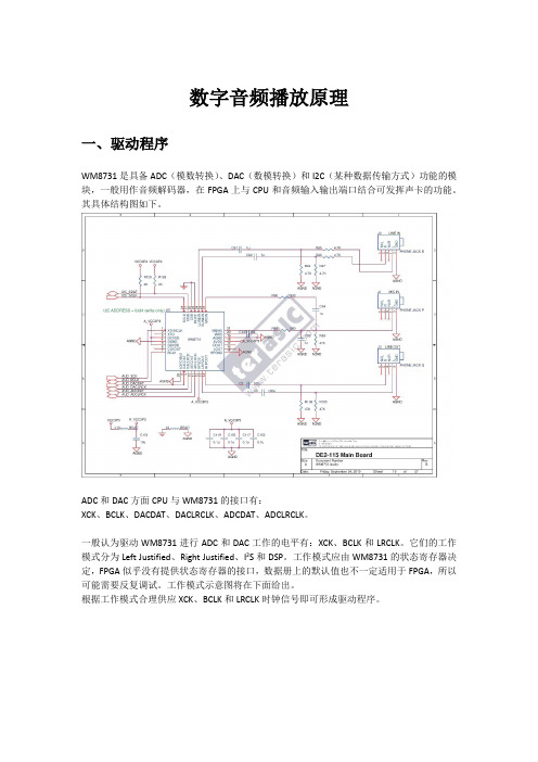
数字音频播放原理一、驱动程序WM8731是具备ADC(模数转换)、DAC(数模转换)和I2C(某种数据传输方式)功能的模块,一般用作音频解码器,在FPGA上与CPU和音频输入输出端口结合可发挥声卡的功能。
其具体结构图如下。
ADC和DAC方面CPU与WM8731的接口有:XCK、BCLK、DACDAT、DACLRCLK、ADCDAT、ADCLRCLK。
一般认为驱动WM8731进行ADC和DAC工作的电平有:XCK、BCLK和LRCLK。
它们的工作模式分为Left Justified、Right Justified、I2S和DSP。
工作模式应由WM8731的状态寄存器决定,FPGA似乎没有提供状态寄存器的接口,数据册上的默认值也不一定适用于FPGA,所以可能需要反复调试。
工作模式示意图将在下面给出。
根据工作模式合理供应XCK、BCLK和LRCLK时钟信号即可形成驱动程序。
以上是LRCLK和BCLK驱动WM8731对ADCDAT(模数转换串行数据)或DACDAT(数模转换串行数据)进行传递和采样的过程。
LRCLK由不同电位决定是向左声道传递还是向右声道传递。
串行数据有字长要求,通过更改状态寄存器,有8、12、16和24位四种字长可供选择。
具体选择需要调试。
以上示意图为驱动程序的理想情况。
实际上WM8731对驱动电平(和输出电平)有具体的延时情况和时间要求。
这分为两种模式,master mode(主)和slave mode(从)。
这里的概念大致如下图所示。
在实验中确实遇到了少量延迟(如case语句)就会带来驱动程序无法驱动WM8731工作的情况。
实验中切换弹奏和自动演奏模式时也需要对驱动程序各时钟进行同步。
以上是采样中数据传递方面的讨论。
下面将涉及到详细采样的过程,这需要主时钟(XCLK 或MCLK)来完成。
具体要求由下表给出。
fs是一个与LRCLK对应的值,个人理解是即在一轮24位数据传递中完成模数转换或数模转换的次数(该次数将会被均分到24位数据中每一位的传递上)。
IIS 接口 详细介绍

1 IIS总线IIS(Integrate Interface of Sound)即集成音频接口,在上个世纪80年代首先被Philips 公司用于消费产品的音频设备,并在一个称为LRCLK(Left/Right CLOCK)的信号机制中经过多路转换,将两路音频信号合成单一的数据队列。
当LRCLK为高时,左声道数据被传输;LRCLK为低时,右声道数据被传输(也可以反过来,高低与左右声音的对应可以自定义)。
对于多通道系统,在同样的BCLK和LRCLK条件下,并行执行几个数据队列也是可能的。
由于IIS、PCM和类似的音频接口不能提供寄存器入口,因此需要独立的控制接口。
IIS总线一般具有4根信号线,如图1所示,包括串行数据输入(IISDI)、串行数据输出(IISD0)、左/右声道选择(IISLRCK)和串行数据时钟(IISCLK);产生IISLRCK和IISCLK 的是主设备。
2 IIS音频驱动实现音频驱动有3种模式:MDD/PDD模式、Wavedev2模式、UAM模式。
它们相同的地方很明显:接口相同,都是流驱动,透过流接口与上层的waveapi.dll交互。
第1种MDD/PDD模式是最早的模式,也是其他驱动常见的分层模式。
如果使用CE提供的MDD(wavem—dd.1ib),会受到一些限制:仅支持一个设备;一个设置仅支持一个流;对循环的支持不大可靠;对流的支持较弱。
当然,由于提供了源码,可以自己修改MDD,突破以上这些限制。
第2种Wavedev2模式,是因为2000年的Smartphone项目产生了新的要求,这些需求需要大改MDD/PDD。
比如上面的限制2,根据CE的开发历史,此时waveapi.dll也不支持software mixer,这就是说只能同时允许一个应用在播放。
所以根据当时情况,CE 的多媒体开发团队设计了Wavedev2模式。
这是一个单体(不分层)的驱动模式,平台相关的模块都在hwctxt.h和hwetxt.cpp中,此外还加入了midi支持、software mixer支持、S/PDlF接口、gain class接口、forcespeaker接口,等等。
基于WinCE5.0下WM8731音频驱动器设计
中图分类号: P 1 . T 3 67
文献标志码 : A
文章编号 :6 3 4 0 (0 1 0 - 0 7 0 17 - 6 2 2 1 ) 1 0 7 4
刘 景 华 , 辛 杰 王
( 岛理工大学 通信 与电子工程学 院, 青 青岛 2 6 3 ) 6 03
摘
要: 论了在 Wi E . 操作 系统 下 , 讨 n 50 C 基于 AT 1 AM9 6 M 平 台 , 9S 2 0AR 控制 WM8 3 音频 芯片的音频驱 71
动设 计 , 在驱动设计 中利用 AT 1 AM9 6 9S 2 0的 S I S C实现对 WM8 3 P和 S 7 1的控制和音频数据传输 , 并在驱动 中设 立多缓冲有效 地提高了语音 数据的实时处理 , 设计 的驱动 器可 以支 持同时 录放 音 , 在实际应 用中取得 并
u e o c n r 1W M 8 3 n r n p r u i a a fo s d t o to 7 1 a d t a s o t a d o d t l w. M o e b fe s a e b i o i p o e r u f r r u l t m r v t
于 AT9 S 1 AM9 6 2 0和 WM8 3 音 频芯 片 的音频 系统 以及驱 动设 计 , 介 绍 了其 实现 方法 . 71 并
1 硬 件 结构
在 本 系统 中采用 AT9 S 1 AM9 6 2 0的 S I 和 S C(I ) 口实现 与 WM8 3 P1 S I 接 S 7 1音频 芯片 的接 口, P 1 S I 实
实验系统LB0介绍

第4章实验器件与实验系统4.3 LB0学习板套件介绍LB0学习板套件是重庆大学通信工程学院为配合改革E DA技术系列课程开发的便携式实验平台。
LB0以Alt era公司的C yclon eⅢ系列FPGAEP3C10E144C8为核心器件,板载大容量存储器,外配丰富的实验模块和扩展接口,可供开展大量的实验项目和实训课题。
LB0学习板套件包含LB0实验板一块、U SB Blaster调试器一个、P S/2数字小键盘一个、7.5V/2A开关电源一个、USB线一条、串口线一条。
LB0学习板套件实物图如图4.1所示。
图4.1 LB0学习板套件实物图LB0电路板硬件结构图如图4.2所示。
图4.2 LB0电路板硬件结构图4.3.1 LB0学习板上模块1.八个LED指示灯模块电路图如图4.3所示,给指定的管脚送高低电平可以点亮或熄灭对应的指示灯,可用于跑马灯、交通灯、其他课题中的状态指示灯等使用。
为方便进行交通灯课题设计,该模块在板上分布为十字交叉形状。
图4.3 八个LED指示灯电路图2.三个拨动开关模块电路图如图4.4所示,通过拨动开关可以调整输入管脚的状态,在板上可以将拨动开关拨上输入高电平,拨下输入低电平。
图4.4 三个拨动开关电路图3、四个按键模块电路图如图4.5所示,通过按键可以产生脉冲信号,按键在未按下时管脚被上拉电阻驱动为高电平,按下为低电平。
由于按键在人为按下时存在机械接触点的抖动导致按键输入信号存在较为严重的抖动,硬件电路中未设计可靠的按键去抖动电路,故在大多数应用中使用按键时需要设计按键去抖动模块对按键信号进行去抖动处理。
图4.5四个按键电路图4、八位动态扫描数码管模块电路图如图4.6所示,电路中每个七段显示模块中包括两位显示码,选用的七段显示模块的管脚图如图4.7所示。
soc文档阅读
一over-viewALSA SoC LayerALSA板上系统层==============The overall project goal of the ALSA System on Chip (ASoC) layer is toprovide better ALSA support for embedded system-on-chip processors (e.g.pxa2xx, au1x00, iMX, etc) and portable audio codecs. Prior to the ASoCsubsystem there was some support in the kernel for SoC audio, however ithad some limitations:-ALSA板上系统(ASoC)层的总体项目目标,是为对SOC嵌入式处理器和便携音频解码器提供更好的ALSA支持。
在ASoC子系统之前,己有对内核的SoC音频支持,但是那些支持存在一些局限:Codec drivers were often tightly coupled to the underlying SoCCPU. This is not ideal and leads to code duplication - for example,Linux had different wm8731 drivers for 4 different SoC platforms.解码器常常与底层嵌入式处理器一对一紧密结合。
这是非理想化的,因为这将导致代码的重复-例如,对四个不同的嵌入式平台,Linux要有不同的wm8731驱动。
(理想的状态是我们可以只有一个wm8731的驱动代码,就可以对应于四个不同的处理器,但由上面说的,解码器-这里的wm8731与底层嵌入式处理器结合过于紧密,无法实现wm8731驱动代码的复用)* There was no standard method to signal user initiated audio events (e.g.Headphone/Mic insertion, Headphone/Mic detection after an insertionevent). These are quite common events on portable devices and often requiremachine specific code to re-route audio, enable amps, etc., after such anevent.没有一个标准的方法可以产生用户初始化音频事件的信号(即,耳机/麦克插入,响应插入事件的耳机/麦克探测)。
ALSA DAPM 介绍
ALSA DAPM/sepnic/article/details/6334922DAPM之一:概述分类:ALSA 2011-04-18 19:151942人阅读评论(0)收藏举报DAPM--Dynamic Audio Power Management,对应结构体是snd_soc_dapm_widget和snd_soc_dapm_route,对应的操作函数是snd_soc_dapm_new_controls()、snd_soc_dapm_add_routes()和snd_soc_dapm_new_widgets()。
在我看来,DAPM是音频驱动初接触者的噩梦。
从何处来,到何处去?它字面上的意义是音频电源动态管理,但是往往困惑于它是怎么被触发的?而最郁闷的是:这方面的资料是最少的,我涉猎多日,却战果寥寥,看来看去还是内核文档dapm.txt最有参考性。
先把这个文档贴上:Dynamic Audio Power Management for Portable Devices===================================================1. Description==============Dynamic Audio Power Management (DAPM) is designed to allow portableLinux devices to use the minimum amount of power within the audiosubsystem at all times. It is independent of other kernel PM and assuch, can easily co-exist with the other PM systems.DAPM is also completely transparent to all user space applications asall power switching is done within the ASoC core. No code changes orrecompiling are required for user space applications. DAPM makes powerswitching decisions based upon any audio stream (capture/playback)activity and audio mixer settings within the device.DAPM spans the whole machine. It covers power control within the entireaudio subsystem, this includes internal codec power blocks and machinelevel power systems.There are 4 power domains within DAPM1. Codec domain - VREF, VMID (core codec and audio power)Usually controlled at codec probe/remove and suspend/resume, althoughcan be set at stream time if power is not needed for sidetone, etc.2. Platform/Machine domain - physically connected inputs and outputsIs platform/machine and user action specific, is configured by themachine driver and responds to asynchronous events e.g when HPare inserted3. Path domain - audio susbsystem signal pathsAutomatically set when mixer and mux settings are changed by the user.e.g. alsamixer, amixer.4. Stream domain - DACs and ADCs.Enabled and disabled when stream playback/capture is started andstopped respectively. e.g. aplay, arecord.All DAPM power switching decisions are made automatically by consulting an audio routing map of the whole machine. This map is specific to each machine and consists of the interconnections between every audio component (including internal codec components). All audio components that effect power are called widgets hereafter.2. DAPM Widgets===============Audio DAPM widgets fall into a number of types:-o Mixer - Mixes several analog signals into a single analog signal.o Mux - An analog switch that outputs only one of many inputs.o PGA - A programmable gain amplifier or attenuation widget.o ADC - Analog to Digital Convertero DAC - Digital to Analog Convertero Switch - An analog switcho Input - A codec input pino Output - A codec output pino Headphone - Headphone (and optional Jack)o Mic - Mic (and optional Jack)o Line - Line Input/Output (and optional Jack)o Speaker - Speakero Supply - Power or clock supply widget used by other widgets.o Pre - Special PRE widget (exec before all others)o Post - Special POST widget (exec after all others)(Widgets are defined in include/sound/soc-dapm.h)Widgets are usually added in the codec driver and the machine driver. There are convenience macros defined in soc-dapm.h that can be used to quickly build alist of widgets of the codecs and machines DAPM widgets.Most widgets have a name, register, shift and invert. Some widgets have extra parameters for stream name and kcontrols.2.1 Stream Domain Widgets-------------------------Stream Widgets relate to the stream power domain and only consist of ADCs (analog to digital converters) and DACs (digital to analog converters).Stream widgets have the following format:-SND_SOC_DAPM_DAC(name, stream name, reg, shift, invert),NOTE: the stream name must match the corresponding stream name in your codec snd_soc_codec_dai.e.g. stream widgets for HiFi playback and captureSND_SOC_DAPM_DAC("HiFi DAC", "HiFi Playback", REG, 3, 1),SND_SOC_DAPM_ADC("HiFi ADC", "HiFi Capture", REG, 2, 1),2.2 Path Domain Widgets-----------------------Path domain widgets have a ability to control or affect the audio signal oraudio paths within the audio subsystem. They have the following form:-SND_SOC_DAPM_PGA(name, reg, shift, invert, controls, num_controls)Any widget kcontrols can be set using the controls and num_controls members.e.g. Mixer widget (the kcontrols are declared first)/* Output Mixer */static const snd_kcontrol_new_t wm8731_output_mixer_controls[] = {SOC_DAPM_SINGLE("Line Bypass Switch", WM8731_APANA, 3, 1, 0),SOC_DAPM_SINGLE("Mic Sidetone Switch", WM8731_APANA, 5, 1, 0),SOC_DAPM_SINGLE("HiFi Playback Switch", WM8731_APANA, 4, 1, 0),};SND_SOC_DAPM_MIXER("Output Mixer", WM8731_PWR, 4, 1,wm8731_output_mixer_controls,ARRAY_SIZE(wm8731_output_mixer_controls)),If you dont want the mixer elements prefixed with the name of the mixer widget,you can use SND_SOC_DAPM_MIXER_NAMED_CTL instead. the parameters are the sameas for SND_SOC_DAPM_MIXER.2.3 Platform/Machine domain Widgets-----------------------------------Machine widgets are different from codec widgets in that they don't have acodec register bit associated with them. A machine widget is assigned to each machine audio component (non codec) that can be independently powered. e.g.o Speaker Ampo Microphone Biaso Jack connectorsA machine widget can have an optional call back.e.g. Jack connector widget for an external Mic that enables Mic Biaswhen the Mic is inserted:-static int spitz_mic_bias(struct snd_soc_dapm_widget* w, int event){gpio_set_value(SPITZ_GPIO_MIC_BIAS, SND_SOC_DAPM_EVENT_ON(event)); return 0;}SND_SOC_DAPM_MIC("Mic Jack", spitz_mic_bias),2.4 Codec Domain----------------The codec power domain has no widgets and is handled by the codecs DAPM event handler. This handler is called when the codec powerstate is changed wrt to any stream event or by kernel PM events.2.5 Virtual Widgets-------------------Sometimes widgets exist in the codec or machine audio map that don't have any corresponding soft power control. In this case it is necessary to createa virtual widget - a widget with no control bits e.g.SND_SOC_DAPM_MIXER("AC97 Mixer", SND_SOC_DAPM_NOPM, 0, 0, NULL, 0), This can be used to merge to signal paths together in software.After all the widgets have been defined, they can then be added to the DAPM subsystem individually with a call to snd_soc_dapm_new_control().3. Codec Widget Interconnections================================Widgets are connected to each other within the codec and machine by audio paths (called interconnections). Each interconnection must be defined in order tocreate a map of all audio paths between widgets.This is easiest with a diagram of the codec (and schematic of the machine audio system), as it requires joining widgets together via their audio signal paths.e.g., from the WM8731 output mixer (wm8731.c)The WM8731 output mixer has 3 inputs (sources)1. Line Bypass Input2. DAC (HiFi playback)3. Mic Sidetone InputEach input in this example has a kcontrol associated with it (defined in example above) and is connected to the output mixer via it's kcontrol name. We can now connect the destination widget (wrt audio signal) with it's source widgets./* output mixer */{"Output Mixer", "Line Bypass Switch", "Line Input"},{"Output Mixer", "HiFi Playback Switch", "DAC"},{"Output Mixer", "Mic Sidetone Switch", "Mic Bias"},So we have :-Destination Widget <=== Path Name <=== Source WidgetOr:-Sink, Path, SourceOr :-"Output Mixer" is connected to the "DAC" via the "HiFi Playback Switch".When there is no path name connecting widgets (e.g. a direct connection) wepass NULL for the path name.Interconnections are created with a call to:-snd_soc_dapm_connect_input(codec, sink, path, source);Finally, snd_soc_dapm_new_widgets(codec) must be called after all widgets and interconnections have been registered with the core. This causes the core toscan the codec and machine so that the internal DAPM state matches thephysical state of the machine.3.1 Machine Widget Interconnections-----------------------------------Machine widget interconnections are created in the same way as codec ones and directly connect the codec pins to machine level widgets.e.g. connects the speaker out codec pins to the internal speaker./* ext speaker connected to codec pins LOUT2, ROUT2 */{"Ext Spk", NULL , "ROUT2"},{"Ext Spk", NULL , "LOUT2"},This allows the DAPM to power on and off pins that are connected (and in use)and pins that are NC respectively.4 Endpoint Widgets===================An endpoint is a start or end point (widget) of an audio signal within themachine and includes the codec. e.g.o Headphone Jacko Internal Speakero Internal Mico Mic Jacko Codec PinsWhen a codec pin is NC it can be marked as not used with a call tosnd_soc_dapm_set_endpoint(codec, "Widget Name", 0);The last argument is 0 for inactive and 1 for active. This way the pin and itsinput widget will never be powered up and consume power.This also applies to machine widgets. e.g. if a headphone is connected to ajack then the jack can be marked active. If the headphone is removed, thenthe headphone jack can be marked inactive.5 DAPM Widget Events====================Some widgets can register their interest with the DAPM core in PM events.e.g. A Speaker with an amplifier registers a widget so the amplifier can bepowered only when the spk is in use./* turn speaker amplifier on/off depending on use */static int corgi_amp_event(struct snd_soc_dapm_widget *w, int event){gpio_set_value(CORGI_GPIO_APM_ON, SND_SOC_DAPM_EVENT_ON(event)); return 0;}/* corgi machine dapm widgets */static const struct snd_soc_dapm_widget wm8731_dapm_widgets =SND_SOC_DAPM_SPK("Ext Spk", corgi_amp_event);Please see soc-dapm.h for all other widgets that support events.5.1 Event types---------------The following event types are supported by event widgets./* dapm event types */#define SND_SOC_DAPM_PRE_PMU 0x1 /* before widget power up */#define SND_SOC_DAPM_POST_PMU 0x2 /* after widget power up */#define SND_SOC_DAPM_PRE_PMD 0x4 /* before widget power down */#define SND_SOC_DAPM_POST_PMD 0x8 /* after widget power down */#define SND_SOC_DAPM_PRE_REG 0x10 /* before audio path setup */#define SND_SOC_DAPM_POST_REG 0x20 /* after audio path setup */DAPM之二:audio paths与dapm kcontrol分类:ALSA 2011-04-20 02:113011人阅读评论(2)收藏举报在用alsa_amixer controls时,除了我们之前提到的snd_soc_add_controls添加的kcontrols 外,还有一些多出来的controls。
采用科里奥利质量流量计的流体黏度测量方法及装置设计
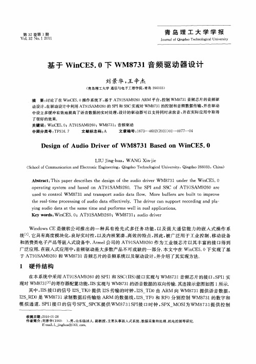
4
2
1、2为传感器敏感管(以F简称传感器霄); 4、5为拾振信号传感器;6为激振器。 图1 科氏流量计结构示意图
当传感器管在驱动装置的驱动下做弯曲振动, 而同时流体从左边进人科氏流量计,通过双C型传 感器管【21后从右边流出时,左边人口段传感器管和 右边出口段传感器管由于受科里奥利力而产生附加 振动,其振动方向相反,因而在两边通过平衡点时产 生时间差,通过测量这个时间差即可检测流体质量 流量。
根据文献[8],知道传感器管具有选频特性,整 个系统为自激系统。由于式(4)需要对谐振频率、 驱动功率进行测量,同时还要对振动状态进行控制, 保持幅值稳定,并且要输出流量等信息,就必须对传 感器管的振动进行测量。由于流体的黏度是随温度
万方数据
变化而变化的,所以也必须得到该黏度值下的温度。 根据这些特点采用了FPGA为核心器件,其系统如 图5所示。
ZHOU B01,REN Jian-xin‘,ZHANG Pen92 (1.College ofAutomation underNoahw∞tern Polytechnical University,ShaanxiXi7口n 710072,China;
2.Xi’dn Dongfeng Machinery&Electronics Co.1zd,Shaanxi Xi’口n 710068。China) Abstract:This paper makes an analysis of the relation between the fluid inner friction and the Corio- lis mass flowmeter’s viberation variables and then puts forward an improved mesurment method.A meas- uring system is designed by using the field programmable gate array as its main component.The experi- ment has proved the improved method is effective.It can extend the application field of the Coriolis mass flowmeter.
- 1、下载文档前请自行甄别文档内容的完整性,平台不提供额外的编辑、内容补充、找答案等附加服务。
- 2、"仅部分预览"的文档,不可在线预览部分如存在完整性等问题,可反馈申请退款(可完整预览的文档不适用该条件!)。
- 3、如文档侵犯您的权益,请联系客服反馈,我们会尽快为您处理(人工客服工作时间:9:00-18:30)。
*@defgroup Audio AUDIO driver
*/
/**@{*/
/**
*@file wm8731.c
*@brief Audio WM8731 CODEC driver source file
*
*
* Copyright (C) 2006 Beijing Emvideo Technology Ltd
regWMRightLineIn &= ~KRLINBOTH;
regWMRightLineIn |= KRINMUTE;
temp = regWMRightLineIn;
break;
case KBoth:
default:
regWMLeftLineIn |= KLRINBOTH;
static uint16 regWMDigitalAudioPathControl = KDAPC;
static uint16 regWMPowerDownControl = KPDC;
static uint16 regWMDigitalAudioInterfaceFormat = KDAIF;
break;
case KBoth:
default:
regWMLeftLineIn |= KLRINBOTH;
regWMLeftLineIn &= ~KLINVOL;
regWMLeftLineIn |= (temp & KLINVOL);
temp = regWMLeftLineIn;
static void wm8731SetDigitalIFFormat(uint32 aFormat);
static void wm8731SetSamplingCtrl(uint32 rate);
static void wm8731SetActive(void);
static void wm8731SetInactive(void);
static void wm8731MuteLineIn(leftRightDirection_t dir);
static void wm8731UnmuteLineIn(leftRightDirection_t dir);
static void wm8731MuteMicIn(void);
static void wm8731UnmuteMicIn(void);
{
uint16 temp;
// max is 100
if (volume > 100)
volume = 100;
// convert percentage volume to HEX
temp = (volume * (KMaxLineInVolume - KMinLineInVolume) / 100) + KMinLineInVolume;
* Codec register control functions
* -------------------------------------------------------------------------------
*/
static void wm8731SetLineInVolume(leftRightDirection_t dir, uint8 volume)
*
*/
#include "wm8731.h"
#include "type.h"
#include "I2C.h"
/***********************************************************************************
static uint8 judge[2];
int OPEN_READ = 1;
int OPEN_WRITE = 1;
/***********************************************************************************
* Global var
*This to store the control word for codec DAC3550a
* ********************************************************************************/
static uint8 mesgbuf[4];
static void wm8731SetHeadPhoneVolume(leftRightDirection_t dir, uint8 volume);
static void wm8731SelectMicIn(void);
static void wm8731SelectLineIn(void);
* Functions to be used
* ********************************************************************************/
static void wm8731SetLineInVolume(leftRightDirection_t dir, uint8 volume);
* Register Contents (sets to default value on power up)
* ********************************************************************************/
static uint16 regWMLeftLineIn = KLLIN;
static uint16 regWMSamplingControl = KSC;
static uint16 regWMActiveControl = KAC;
/***********************************************************************************
static uint32 driver_busy;
static uint32 open_mode;
static uint8 gVolumeL = 250, gVolumeR = 250;
static uint8 gGainL = 250, gGainR = 250;
/***********************************************************************************
regWMLeftLineIn |= KLINMUTE;
temp = regWMLeftLineIn;
break;
}
mesgbuf[0] = temp >> 8;
mesgbuf[1] = temp & 0x00FF;
i2c_wm8731_write(mesgbuf, 2, 0);
{
uint16 temp;
switch(dir)
{
case KLeft:
regWMLeftLineIn |= KLINMUTE;
temp = regWMLeftLineIn;
break;
case KRight:
temp = regWMLeftLineIn;
static void wm8731EnableBypass(void);
static void wm8731DisableBypass(void);
static void wm8731EnableMicBoost(void);
static void wm8731DisableMicBoost(void);
static void wm8731Reset(void);
static void wm8731_poweron(void);
static void wm8731_set_rate(int rate);
/* -------------------------------------------------------------------------------
static void wm8731SetAnalogPathCtrl(uint32 aCtrl);
static void wm8731SetDigitalPathCtrl(uint32 aCtrl);
static void wm8731UnmuteDAC(void);
static void wm8731MuteDAC(void);
switch(dir)
{
case KLeft:
regWMLeftLineIn &= ~KLRINBOTH;
regWMLeftLineIn &= ~KLINVOL;
regWMLeftLineIn |= (temp & KLINVOL);
temp = regWMLeftLineIn;
static void wm8731DisableDeemphasis(void);
static void wm8731SetStandbyMode(void);
static void wm8731SetRunningMode(void);
static void wm8731SetSuspendMode(void);
break;
case KRight: