1N5391中文资料
SM5391中文资料

FEATURES
* Ideal for surface mounted applications * Low leakage current * Glass passivated junction
SM-1(DO-213AB)
MECHANICAL DATA
* Case: Molded plastic * Epoxy: UL 94V-0 rate flame retardant * Terminals: Solder plated solderable per MIL-STD-202E, Method 208 guaranteed * Polarity: Color band denotes cathode end * Mounting position: Any * Weight: 0.12 gram .205(5.2) .190(4.8) SOLDERABLE ENDS
SYMBOL Maximum Recurrent Peak Reverse Voltage Maximum RMS Voltage Maximum DC Blocking Voltage Maximum Average Forward Rectified Current T A = 75 C Peak Forward Surge Current I FM(surge): 8.3 ms single half sine-wave superimposed on rated load (JEDEC Method) Maximum Forward Voltage at 1.5A DC Maximum DC Reverse Current at Rated DC Blocking Voltage Typical Thermal Resistance (Note 2) Typical Junction Capacitance (Note 1) Operating and Storage Temperature Range @T A = 25 o C @T A = 125 C RθJC CJ T J , T STG
1N5310UR-1中文资料

0.748 0.825 0.902 1.001 1.100
1.210 1.32 1.43 1.54 1.65
1.76 1.98 2.20 2.42 2.64
2.97 3.30 3.63 3.96 4.29
4.73 5.17
MINIMUM DYNAMIC IMPEDANCE @VS = 25V
0.39 0.43 0.47 0.56 0.62
0.68 0.75 0.82 0.91 1.00
1.10 1.20 1.30 1.40 1.50
1.60 1.80 2.00 2.20 2.40
2.70 3.00 3.30 3.60 3.90
4.30 4.70
MIN
0.198 0.216 0.243 0.270 0.297
CDLL5303 CDLL5304 CDLL5305 CDLL5306 CDLL5307
CDLL5308 CDLL5309 CDLL5310 CDLL5311 CDLL5312
CDLL5313 CDLL5314
REGULATOR CURRENT l p (mA) @ VS = 25V
NOM
0.22 0.24 0.27 0.30 0.33
• METALLURGICALLY BONDED
1N5283UR-1 thru 1N5314UR-1 and
CDLL5283 thru CDLL5314
MAXIMUM RATINGS
Operating Temperature: -65°C to +175°C
Storage Temperature: -65°C to +175°C
proteus元件名称中英文对照表

元件名称中英文名说明7407 驱动门1N914 二极管74Ls00 与非门74LS04 非门74LS08 与门74LS390 TTL 双十进制计数器7SEG 4针BCD-LED 输出从0-9 对应于4根线的BCD码7SEG 3-8译码器电路BCD-7SEG转换电路ALTERNATOR 交流发电机AMMETER-MILLI mA安培计AND 与门BA TTERY 电池/电池组BUS 总线CAP 电容CAPACITOR 电容器CLOCK 时钟信号源CRYSTAL 晶振D-FLIPFLOP D触发器FUSE 保险丝GROUND 地LAMP 灯LED-RED 红色发光二极管LM016L 2行16列液晶可显示2行16列英文字符,有8位数据总线D0-D7,RS,R/W,EN三个控制端口(共14线),工作电压为5V。
没背光,和常用的1602B功能和引脚一样(除了调背光的二个线脚)LOGIC ANAL YSER 逻辑分析器LOGICPROBE 逻辑探针LOGICPROBE[BIG] 逻辑探针用来显示连接位置的逻辑状态LOGICSTATE 逻辑状态用鼠标点击,可改变该方框连接位置的逻辑状态LOGICTOGGLE 逻辑触发MASTERSWITCH 按钮手动闭合,立即自动打开MOTOR 马达OR 或门POT-LIN 三引线可变电阻器POWER 电源RES 电阻RESISTOR 电阻器SWITCH 按钮手动按一下一个状态SW-SPDT-mom 二选通一按钮触发开关BUTTONVOLTMETER 伏特计VOLTMETER-MILLI mV伏特计VTERM 串行口终端Electromechanical 电机Inductors 变压器Laplace Primitives 拉普拉斯变换Memory IcsMicroprocessor IcsMiscellaneous 各种器件AERIAL-天线;ATAHDD;ATMEGA64;BATTERY;CELL;CRYSTAL-晶振;FUSE;METER-仪表;Modelling Primitives 各种仿真器件是典型的基本元器模拟,不表示具体型号,只用于仿真,没有PCBOptoelectronics 各种发光器件发光二极管,LED,液晶等等PLDs & FPGAsResistors 各种电阻Simulator Primitives 常用的器件Speakers & SoundersSwitches & Relays 开关,继电器,键盘BUTTON 触发开关Switching Devices 晶阊管Transistors 晶体管(三极管,场效应管)TTL 74 seriesTTL 74ALS seriesTTL 74AS seriesTTL 74F seriesTTL 74HC seriesTTL 74HCT seriesTTL 74LS seriesTTL 74S seriesAnalog Ics 模拟电路集成芯片Capacitors 电容集合CMOS 4000 seriesConnectors 排座,排插Data Converters ADC,DACDebugging Tools 调试工具7SEG 数码管ECL 10000 Series 各种常用集成电路1.电阻固定电阻:RES半导体电阻:RESSEMT电位计;POT变电阻;RV AR可调电阻;res1可变电阻pot2.电容定值无极性电容;CAP定值有极性电容;CAP半导体电容:CAPSEMI可调电容:CAPV AR3.电感:INDUCTOR4.二极管:DIODE.LIB发光二极管:LED5.三极管:NPN16.结型场效应管:JFET.lib7.MOS场效应管8.MES场效应管9.继电器:PELAY. LIB10.灯泡:LAMP11.运放:OPAMP12.数码管:7-SEG_DP (MISCELLANEOUS DEVICES.LIB)13.开关;sw_pb原理图常用库文件:Miscellaneous Devices.ddbDallas Microprocessor.ddbIntel Databooks.ddbProtel DOS Schematic Libraries.ddbPCB元件常用库:Advpcb.ddbGeneral IC.ddbMiscellaneous.ddb部分分立元件库元件名称及中英对照AND 与门ANTENNA 天线BA TTERY 直流电源BELL 铃,钟BVC 同轴电缆接插件BRIDEG 1 整流桥(二极管) BRIDEG 2 整流桥(集成块) BUFFER 缓冲器BUZZER 蜂鸣器CAP 电容CAPACITOR 电容CAPACITOR POL 有极性电容CAPV AR 可调电容CIRCUIT BREAKER 熔断丝COAX 同轴电缆CON 插口CRYSTAL 晶体整荡器DB 并行插口DIODE 二极管DIODE SCHOTTKY 稳压二极管DIODE V ARACTOR 变容二极管DPY_3-SEG 3段LEDDPY_7-SEG 7段LEDDPY_7-SEG_DP 7段LED(带小数点) ELECTRO电解电容FUSE 熔断器INDUCTOR 电感INDUCTOR IRON 带铁芯电感INDUCTOR3 可调电感JFET N N沟道场效应管JFET P P沟道场效应管LAMP 灯泡LAMP NEDN 起辉器LED 发光二极管METER 仪表MICROPHONE 麦克风MOSFET MOS管MOTOR AC 交流电机MOTOR SERVO 伺服电机NAND 与非门NOR 或非门NOT 非门NPN NPN三极管NPN-PHOTO 感光三极管OPAMP 运放OR 或门PHOTO 感光二极管PNP 三极管NPN DAR NPN三极管PNP DAR PNP三极管POT 滑线变阻器PELAY-DPDT 双刀双掷继电器RES1.2 电阻RES3.4 可变电阻RESISTOR BRIDGE ? 桥式电阻RESPACK ? 电阻SCR 晶闸管PLUG ? 插头PLUG AC FEMALE 三相交流插头SOCKET ? 插座SOURCE CURRENT 电流源SOURCE VOLTAGE 电压源SPEAKER扬声器SW ? 开关SW-DPDY ? 双刀双掷开关SW-SPST ? 单刀单掷开关SW-PB 按钮THERMISTOR 电热调节器TRANS1 变压器TRANS2 可调变压器TRIAC ? 三端双向可控硅TRIODE ? 三极真空管V ARISTOR 变阻器ZENER ? 齐纳二极管DPY_7-SEG_DP 数码管SW-PB 开关其他元件库Protel Dos Schematic 4000 Cmos .Lib (40.系列CMOS管集成块元件库)4013 D 触发器4027 JK 触发器Protel Dos Schematic Analog Digital.Lib(模拟数字式集成块元件库)AD系列DAC系列HD系列MC系列Protel Dos Schematic Comparator.Lib(比较放大器元件库)Protel Dos Shcematic Intel.Lib(INTEL公司生产的80系列CPU集成块元件库)Protel Dos Schematic Linear.lib(线性元件库)例555Protel Dos Schemattic Memory Devices.Lib(内存存储器元件库)Protel Dos Schematic SYnertek.Lib(SY系列集成块元件库)Protes Dos Schematic Motorlla.Lib(摩托罗拉公司生产的元件库)Protes Dos Schematic NEC.lib(NEC公司生产的集成块元件库)Protes Dos Schematic Operationel Amplifers.lib(运算放大器元件库)Protes Dos Schematic TTL.Lib(晶体管集成块元件库74系列)Protel Dos Schematic Voltage Regulator.lib(电压调整集成块元件库)Protes Dos Schematic Zilog.Lib(齐格格公司生产的Z80系列CPU集成块元件库)元件属性对话框中英文对照Lib ref 元件名称Footprint 器件封装Designator 元件称号Part 器件类别或标示值Schematic Tools 主工具栏Writing Tools 连线工具栏Drawing Tools 绘图工具栏稳压二极管ZENER DIODE肖特基二极管SCHOTTKY DIODE二极管DIODE变容二极管V ARIODE三极管TRANSISTOR电感INDUCTOR磁环EMIFIL电阻RESISTOR电容CAPACITY晶振CRYSTAL涤纶电容MYLAR CAP电解电容ELECT CAP瓷片电容CERAMIC CAP安规电容FILM CAPProtel 99 se的元件中英文PcbRe: [分享] protel99se 元件名系表--分立元件库中英文对照电阻AXIAL 无极性电容RAD 电解电容RB- 电位器VR 二极管DIODE 三极管TO 电源稳压块78和79系列TO-126H和TO-126V 场效应管和三极管一样整流桥D-44 D-37 D-46 单排多针插座CON SIP 双列直插元件DIP 晶振XTAL1电阻:RES1,RES2,RES3,RES4;封装属性为axial系列无极性电容:cap;封装属性为RAD-0.1到rad-0.4电解电容:electroi;封装属性为rb.2/.4到rb.5/1.0电位器:pot1,pot2;封装属性为vr-1到vr-5二极管:封装属性为diode-0.4(小功率)diode-0.7(大功率)三极管:常见的封装属性为to-18(普通三极管)to-22(大功率三极管)to-3(大功率达林顿管)电源稳压块有78和79系列;78系列如7805,7812,7820等79系列有7905,7912,7920等常见的封装属性有to126h和to126v整流桥:BRIDGE1,BRIDGE2: 封装属性为D系列(D-44,D-37,D-46)电阻:其中指电阻的长度,一般用AXIAL0.4瓷片电容:。
1N942BUR-1中文资料

元器件交易网
Pd, Rated Power Dissipation (mW)
CDLL941 CDLL945B
thru
600 500 400 300 200 100 0 0 25 50 75 100 125 TL, Ambient temperature (°C) 150 175
FIGURE 4
ZENER IMPEDANCE VS. OPERATING CURRENT
mA 7.5 7.5 7.5 7.5 7.5 7.5 7.5 7.5 7.5 7.5 7.5 7.5 7.5 7.5 7.5
OHMS 30 30 30 30 30 30 30 30 30 30 30 30 30 30 30
DESIGN DATA
CASE: DO-213AA, Hermetically sealed glass case. (MELF, SOD-80, LL34) LEAD FINISH: Tin / Lead POLARITY: Diode to be operated with the banded (cathode) end positive. MOUNTING POSITION: Any. MOUNTING SURFACE SELECTION: The Axial Coefficient of Expansion (COE) Of this Device is Approximately +6PPM/°C. The COE of the Mounting Surface System Should Be Selected To Provide A Suitable Match With This Device.
1N941BUR-1 thru1N945BUR-1 and CDLL941 thru CDLL945B
1N5711;中文规格书,Datasheet资料

1/3®1N5711SMALL SIGNAL SCHOTTKY DIODEOctober 2001 - Ed: 1BSymbol ParameterValue Unit V RRM Repetitive Peak Reverse Voltage 70V I F Forward Continuous Current*T a = 25°C 15mA P tot Power Dissipation*T a = 25°C430mW T stg T j Storage and Junction Temperature Range- 65 to 200- 65 to 200°C T LMaximum Lead Temperature for Soldering during 10s at 4mm from Case230°CABSOLUTE RATINGS (limiting values)Symbol Test ConditionsValue Unit R th(j-a)Junction-ambient*400°C/WTHERMAL RESISTANCE* On infinite heatsink with 4mm lead length **Pulse test: t p ≤300µs δ<2%.Matched batches available on request. Test conditions (forward voltage and/or capacitance) according to customer specification.Symbol Test Conditions Min.Typ.Max.Unit V BR T amb = 25°C I R = 10µA 70V V F * *T amb = 25°C I F = 1mA 0.41VT amb = 25°CI F = 15mA 1I R * *T amb = 25°CV R = 50V0.2µASTATIC CHARACTERISTICSELECTRICAL CHARACTERISTICS Symbol Test Conditions Min.Typ.Max.Unit C T amb = 25°C V R = 0V f = 1MHz 2pF τT amb = 25°CI F = 5mAKrakauer Method100psDYNAMIC CHARACTERISTICSMetal to silicon junction diode featuring high break-down, low turn-on voltage and ultrafast switching.Primarly intended for high level UHF/VHF detec-tion and pulse application with broad dynamic range. Matched batches are available on requestDESCRIPTION1N5711Fig.1:Forward current versus forward voltage atlow level (typical values).Fig.2:Capacitance C versus reverse applied voltage V R (typical values).Fig.3:Reverse current versus ambient tempera-ture.Fig.4:Reverse current versus continuous reverse voltage (typical values).Cooling method : by convection and conductionMarking: clear, ring at cathode end.Weight: 0.15gInformation furnished is believed to be accurate and reliable.However,STMicroelectronics assumes no responsibility for the consequences of use of such information nor for any infringement of patents or other rights of third parties which may result from its use.No license is granted by implication or otherwise under any patent or patent rights of STMicroelectronics.Specifications mentioned in this publication are subject to change without notice. This publication supersedes and replaces all information previously supplied.STMicroelectronics products are not authorized for use as critical components in life support devices or systems without express written approval of STMicroelectronics.The ST logo is a registered trademark of STMicroelectronics© 2001 STMicroelectronics - Printed in Italy - All rights reserved.STMicroelectronics GROUP OF COMPANIESAustralia - Brazil - China - Finland - France - Germany - Hong Kong - India - Italy - Japan - Malaysia Malta - Morocco - Singapore - Spain - Sweden - Switzerland - United Kingdom - U.S.A.分销商库存信息: STM1N5711。
1N5391-1N5399中文资料,PDF资料
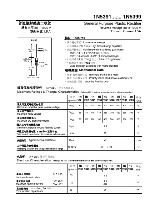
1N 53921N 53931N 53941N 53951N 53961N 53971N 53988001002003004005006001002003004005006008007014028035042056045501.51.2V 5.0200μA pFI R1N5391 ...... 1N53991N 5399100010007001N 5391505035201N 53921N 53931N 53941N 53951N 53961N 53971N 53981N53991N 5391普通塑封整流二极管反向电压 50 ---1000 V正向电流 1.5 AGeneral Purpose Plastic RectifierReverse Voltage 50 to 1000 VForward Current 1.5A210Cj最大正向电压 I F = 1.5A 最大反向电流 TA= 25℃典型结电容 V R = 4.0V, f = 1MHz TA=100℃ Maximum forward voltageMaximum reverse current Type junction capacitanceVF符号Symbols 单位Unit电特性 TA = 25℃ 除非另有规定。
Electrical Characteristics Ratings at 25℃ ambient temperature unless otherwise specified.最大可重复峰值反向电压Maximum repetitive peak reverse voltage 最大均方根电压 Maximum RMS voltage 最大直流阻断电压Maximum DC blocking voltage最大正向平均整流电流Maximum average forward rectified current 峰值正向浪涌电流 8.3ms单一正弦半波Peak forward surge current 8.3 ms single half sine-wave典型热阻 Typical thermal resistance工作结温和存储温度Operating junction and storage temperature range-55 --- +150 V V V A A℃/WV RRM V RMS V DC I F(AV)I FSM ℃Tj, TSTG极限值和温度特性 TA = 25℃ 除非另有规定。
1N5817,1N5758,1N5819(中文)

V V 21℃1N58171N5818AV A mA 301.00.5500.875251.0101N581920401428110pF 0.4500.7500.6000.900@IF = 1.0A @IF = 3.0A 单位UnitV V R(RMS)·正向压降低。
Low Forward Voltage Drop最大正向平均整流电流最大峰值反向电压最大反向有效值电压- 50 --- +150V RRM I FM ·大电流承受能力。
High Current Capability塑封肖特基二极管最大正向电压降V F 正向峰值浪涌电流 8.3mS单一正弦半波I FSM 最大反向漏电流IR 典型热阻工作温度和存储温度Tj, T STG典型结电容 V R = 4.0V, f = 1.0MHzCj @TA = 25℃@TA = 100℃·高温焊接保证 High temperature soldering guaranteed:250℃/10 秒, 0.375" (9.5mm)引线长度。
250℃/10 seconds, 0.375" (9.5mm) lead length,·引线可承受5 磅(2.3kg) 拉力。
5 lbs. (2.3kg) tension机械数据 Mechanical Data·端子: 镀锡轴向引线 Terminals: Plated axial leads·极性: 色环端为负极 Polarity: Color band denotes cathode end ·安装位置: 任意 Mounting Position: Any特征 FeaturesPLASTIC SCHOTTKY BARRIER RECTIFIERMaximum repetitive peak reverse voltageMaximum RMS voltage最大直流阻断电压Maximum DC blocking voltageMaximum average forward rectified currentMaximum forward voltage Peak forward surge current 8.3 ms single half sine-waveMaximum reverse current Typical thermal resistanceOperating junction and storage temperature rangeType junction capacitance极限值和电参数 TA = 25℃ 除非另有规定。
1N5241中文资料
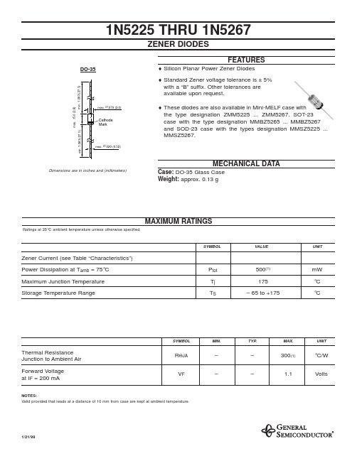
Maximum Reverse Leakage Current Test Voltage IR (µA) 50 25 15 10 5.0 5.0 5.0 5.0 5.0 5.0 3.0 3.0 3.0 3.0 3.0 3.0 2.0 1.0 0.5 0.1 0.1 0.1 0.1 0.1 0.1 0.1 0.1 0.1 0.1 0.1 0.1 0.1 0.1 0.1 0.1 0.1 0.1 0.1 0.1 0.1 0.1 0.1 0.1 VR (V) 1.0 1.0 1.0 1.0 1.0 2.0 2.0 3.0 3.5 4.0 5.0 6.0 6.5 6.5 7.0 8.0 8.4 9.1 9.9 10 11 12 13 14 14 15 17 18 19 21 21 23 25 27 30 33 36 39 43 46 47 52 56
元器件交易网
1N5225 THRU 1N5267
ZENER DIODES
FEATURES
DO-35
min. 1.083 (27.5)
♦ Silicon Planar Power Zener Diodes ♦ Standard Zener voltage tolerance is ± 5% with a “B” suffix. Other tolerances are available upon request.
NOTES: (1) The Zener impedance is derived from the 1 kHz AC voltage which results when an AC current having an RMS value equal to 10% of the Zener current (IZT or IZK) is superimposed on IZT or IZK. Zener impedance is measured at two points to insure a sharp knee on the breakdown curve and to eliminate unstable units (2) Valid provided that leads at a distance of 10 mm from case are kept at ambient temperature (3) Measured with device junction in thermal equilibrium
1N5311UR-1中文资料
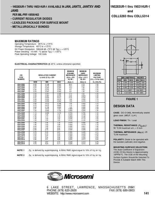
1N5283UR-1 thru 1N5314UR-1 and CDLL5283 thru CDLL5314
MAXIMUM RATINGS
Operating Temperature: -65°C to +175°C Storage Temperature: -65°C to +175°C DC Power Dissipation: 500mW @ +75°C @ TEC = +125°C Power Derating: 10 mW / °C above TEC = +125°C Peak Operating Voltage: 100 Volts
MAXIMUM LIMITING VOLTAGE @ lL = 0.8 lp (min) VL (VOLTS) 1.00 1.00 1.00 1.00 1.00 1.05 1.05 1.05 1.10 1.13 1.15 1.20 1.25 1.29 1.35 1.40 1.45 1.50 1.55 1.60 1.65 1.75 1.85 1.95 2.00 2.15 2.25 2.35 2.50 2.60 2.75 2.90
DIM D F G G1 S
MILLIMETERS MIN MAX 2.39 2.66 0.41 0.55 4.80 5.20 4.11 REF. 0.03 MIN.
INCHES MIN MAX .094 .105 .016 .022 .189 .205 .159 REF. .001 MIN.
FIGURE 1
FIGURE 2 TEMPERATURE COEFFICIENT
TC,TEMPERATURE COEFFICIENT
1.0 0.8 0.6 0.4 0.2 0 -0.2 -0.4 -0.6 -0.8 -1.0 0.2 0.3 0.4 0.5 0.6 0.7 0.8 0.9 1.0 2.0 3.0 4.0 5.0 RANGE TYPICAL
vishay 1n5391 通用塑料整流器 数据表说明书

General Purpose Plastic RectifierFEATURES•Low forward voltage drop •Low leakage current•High forward surge capability•Solder dip 275 °C max. 10 s, per JESD 22-B106•Material categorization: for definitions of compliance please see /doc?99912TYPICAL APPLICATIONSFor use in general purpose rectification of power supplies, inverters, converters, and freewheeling diodes application.MECHANICAL DATACase: DO-41 (DO-204AL), molded epoxy bodyMolding compound meets UL 94 V-0 flammability rating Base P/N-E3 - RoHS-compliant, commercial grade Terminals: matte tin plated leads, solderable per J-STD-002 and JESD 22-B102E3 suffix meets JESD 201 class 1A whisker test Polarity: color band denotes cathode endPRIMARY CHARACTERISTICSI F(AV) 1.5 AV RRM 50 V, 100 V, 200 V, 300 V, 400 V, 500 V, 600 V, 800 V, 1000 VI FSM 50 A V F 1.4 V I R 5.0 μA T J max.150 °C Package DO-41 (DO-204AL)Circuit configurationSingleDO-41 (DO-204AL)MAXIMUM RATINGS (T A = 25 °C unless otherwise noted)PARAMETERSYMBOL 1N53911N53921N53931N53941N53951N53961N53971N53981N5399UNIT Maximum repetitive peak reverse voltage V RRM 501002003004005006008001000V Maximum RMS voltage V RMS 3570140210280350420560700V Maximum DC blocking voltage V DC 501002003004005006008001000V Maximum average forwardrectified current 0.500" (12.7 mm) lead length at T L = 70 °C I F(AV)1.5APeak forward surge current 8.3 ms single half sine-wave superimposed on rated load I FSM50AMaximum full load reversecurrent, full cycle average 0.375" (9.5 mm) lead length at T L = 70 °C I R(AV)300μA Operation junction and storage temperature rangeT J , T STG-50 to +150°CNote(1)Thermal resistance from junction to ambient at 0.375" (9.5 mm) lead length, PCB mountedRATINGS AND CHARACTERISTICS CURVES (T A = 25 °C unless otherwise noted)Fig. 1 - Forward Current Derating Curve Fig. 2 - Maximum Non-repetitive Peak Forward Surge CurrentELECTRICAL CHARACTERISTICS (T A = 25 °C unless otherwise noted)PARAMETER TEST CONDITIONS SYMBOL 1N53911N53921N53931N53941N53951N53961N53971N53981N5399UNIT Maximum instantaneous forward voltage 1.5 AT A = 70 °C V F1.4 V Maximum DC reverse current at rated DC blocking voltage T A = 25 °CI R5.0μAT A = 150 °C300Typical reverse recovery time I F = 0.5 A, I R = 1.0 A, I rr = 0.25 A t rr 2.0μs Typical junction capacitance4.0 V, 1 MHzC J15pFTHERMAL CHARACTERISTICS (T A = 25 °C unless otherwise noted)PARAMETERSYMBOL 1N53911N53921N53931N53941N53951N53961N53971N53981N5399UNIT Typical thermal resistanceR θJA (1)55°C/WR θJL (1)25ORDERING INFORMATION (Example)PREFERRED P/N UNIT WEIGHT (g)PREFERRED PACKAGE CODEBASE QUANTITYDELIVERY MODE1N5391-E3/540.33654550013" diameter paper tape and reel1N5391-E3/730.336733000Ammo pack packaging01.01.52.02550751001251501750.5Lead Temperature (°C)A v e r a g e F o r w a r d R e c t i fi e d C u r r e n t (A )01020305040110010Number of Cycle s at 60 HzP e a k F o r w a r d S u r g e C u r r e n t (A )Fig. 3 - Typical Instantaneous Forward Characteristics Fig. 4 - Typical Reverse Characteristics Fig. 5 - Typical Junction CapacitanceFig. 6 - Transient Thermal ImpedancePACKAGE OUTLINE DIMENSIONS in inches (millimeters)0.60.8 1.0 1.2 1.4 1.6 1.80.010.1101100I n s t a n t a n e o u s F o r w a r d C u r r e n t (A )In s tantaneou sForward Voltage (V)604020100800.010.11010010001Percent of Rated Peak Rever s e Voltage (%)I n s t a n t a n e o u s R e v e r s e L e a k a g e C u r r e n t (μA )0.1101100100101Rever s e Voltage (V)J u n c t i o n C a p a c i t a n c e (p F)1001010.1t - Pul s e Duration (s )0.010.1110100T r a n s i e n t T h e r m a l I m p e d a n c e (°C /W )DO-41 (DO-204AL)Legal Disclaimer Notice VishayDisclaimerALL PRODUCT, PRODUCT SPECIFICATIONS AND DATA ARE SUBJECT TO CHANGE WITHOUT NOTICE TO IMPROV E RELIABILITY, FUNCTION OR DESIGN OR OTHERWISE.V ishay Intertechnology, Inc., its affiliates, agents, and employees, and all persons acting on its or their behalf (collectively,“Vishay”), disclaim any and all liability for any errors, inaccuracies or incompleteness contained in any datasheet or in any other disclosure relating to any product.Vishay makes no warranty, representation or guarantee regarding the suitability of the products for any particular purpose or the continuing production of any product. To the maximum extent permitted by applicable law, Vishay disclaims (i) any and all liability arising out of the application or use of any product, (ii) any and all liability, including without limitation special, consequential or incidental damages, and (iii) any and all implied warranties, including warranties of fitness for particular purpose, non-infringement and merchantability.Statements regarding the suitability of products for certain types of applications are based on Vishay's knowledge of typical requirements that are often placed on Vishay products in generic applications. Such statements are not binding statements about the suitability of products for a particular application. It is the customer's responsibility to validate that a particular product with the properties described in the product specification is suitable for use in a particular application. Parameters provided in datasheets and / or specifications may vary in different applications and performance may vary over time. All operating parameters, including typical parameters, must be validated for each customer application by the customer's technical experts. Product specifications do not expand or otherwise modify Vishay's terms and conditions of purchase, including but not limited to the warranty expressed therein.Hyperlinks included in this datasheet may direct users to third-party websites. These links are provided as a convenience and for informational purposes only. Inclusion of these hyperlinks does not constitute an endorsement or an approval by Vishay of any of the products, services or opinions of the corporation, organization or individual associated with the third-party website. Vishay disclaims any and all liability and bears no responsibility for the accuracy, legality or content of the third-party website or for that of subsequent links.Except as expressly indicated in writing, Vishay products are not designed for use in medical, life-saving, or life-sustaining applications or for any other application in which the failure of the Vishay product could result in personal injury or death. Customers using or selling Vishay products not expressly indicated for use in such applications do so at their own risk. Please contact authorized Vishay personnel to obtain written terms and conditions regarding products designed for such applications. No license, express or implied, by estoppel or otherwise, to any intellectual property rights is granted by this document or by any conduct of Vishay. Product names and markings noted herein may be trademarks of their respective owners.© 2022 VISHAY INTERTECHNOLOGY, INC. ALL RIGHTS RESERVED。
1N5391
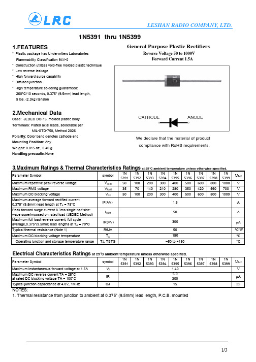
1.FEATURES* Plastic package has Underwriters Laboratories Flammability Classification 94V-0* Construction utilizes void-free molded plastic technique * Low reverse leakage * High forward surge capability * Diffused junction* High temperature soldering guaranteed: 260°C/10 seconds, 0.375" (9.5mm) lead length, 5 lbs. (2.3kg) tension2.Mechanical DataCase : JEDEC DO-15, molded plastic body Terminals : Plated axial leads, solderable per MIL-STD-750, Method 2026Polarity : Color band denotes cathode end Mounting Position : Any Weight : 0.015 oz., 0.40 gHandling precautin :None3.Maximum Ratings & Thermal Characteristics Ratings at 25°C ambient temperature unless otherwise specified.Parameter Symbolsymbol 1N 53911N53921N 53931N 53941N 53951N 53961N 53971N 53981N 5399Unit Maximum repetitive peak reverse voltage V RRM 501002003004005006008001000V Maximum RMS voltage V RMS 3570140210280350420560700V Maximum DC blocking voltageV DC 501002003004005006008001000V Maximum average forward rectified current 0.375" (9.5mm) lead length at T A = 75°CIF(AV) A Peak forward surge current 8.3ms single half sine-wave superimposed on rated load (JEDEC Method)I FSM A Maximum full load reverse current, full cycleaverage,0.375"(9.5mm) lead lengths at T A = 70°C IR(AV)µA Typical thermal resistance (Note 1) R θJA °C/W Maximum DC blocking voltage temperature T A °C Operating junction and storage temperature rangeTJ, TSTG°CElectrical Characteristics Ratings at 25°C ambient temperature unless otherwise specified.Parameter Symbolsymbol 1N 53911N 53921N 53931N 53941N 53951N 53961N 53971N 53981N 5399Unit Maximum instantaneous forward voltage at 1.5A V F V Maximum DC reverse current TA = 25°C at rated DC blocking voltage TA = 100°C IR µA Typical junction capacitance at 4.0V, 1MHzCJPFNOTES:1. Thermal resistance from junction to ambient at 0.375” (9.5mm) lead length, P.C.B. mounted50150–50 to +1501.405.0300151.5503001N5391 thru 1N5399General Purpose Plastic RectifiersReverse Voltage 50 to 1000V Forward Current 1.5AWe declare that the material of productcompliance with RoHS requirements.4.Ratings and Characteristic Curves ( TA = 25°C unless otherwise noted )Fig. 1 – Forward Current Derating CurveFig. 2 – Maximum Non-repetitive PeakA v e r a g e F o r w a r d R e c t i f i e d C u r r e n t (A )I n s t a n t a n e o u s F o r w a r d C u r r e n t (A )0.1 1 10 1001.00.10.01102.01.0Reverse Voltage (V)T r a n s i e n t t h e r m a l i m p e d a n c e (°C /W )101.00.11000.01 0.1 1.0 10 100t,Pulse duration,sec5.Package Dimensions in inches and (millmeters)Unit:mmA :卷盘规格/Reel spec.ItemSymbol Dimension A 76.4±0.1B 82.5±0.2C 330±0.5Width W72±0.2ThicknessW13±0.2B :外箱规格/Outer Box SpecificationItem Symbol Dimension L 350±2W 350±2H340±4按以上包装方式:(As per the above spec)DO-154K 16KQ'ty/Taping 5K 1.4K Q'ty/Packing Case20K5.6KSize外型/Outside DO-41 & A-405DO-201AD Packing Of Plastic-Sealed Axial Lead DiodesDimeter 1.卷盘/Reel Packing (52mm )Unit:mmA : 弹带盒规格/Ammo Box Spec.ItemSymbol Dimension Notes L 260±2W 76±2H 100±4L 250±3W 45±3H 95±5ItemSymbol Dimension Notes L 430±2W 280±2H 225±4L 435±3W 280±3H295±5L按以上包装方式:(As per the above spec)DO-152K 20K40K 2. 弹带盒装/Ammo PackingQ'ty/Packing Case 52mm/TYPE60K 14.4KQ'ty/Taping 3K0.8K Q'ty/Packing Case 26mm/TYPE 30K7.2KCase's Size52mm TYPE 26mm TYPE外型/OutsideA-405 & DO-41 & R-1DO-201AD Box's Size52mm TYPE 26mm TYPEA.包装盒尺寸/Box Dimension( DO-41&DO-15 )ItemSymbol DimensionL 200±2W 84±2H21±2( DO-201AD )Item Symbol Dimension L 200±2W 84±2H29±2B :外箱规格/Outer Box SpecificationItemSymbol Dimension L 465±2W 225±2H260±4A按以上包装方式:(As per the above spec)DO-150.5K 25K3. 散装/Bulk Packing Q'ty/Taping 1K0.3KQ'ty/Packing Case50K12K外型/OutsideDO-41&A-405&R-1DO-201AD Box's SizeCase's SizeBox's SizeUnit:mm注: 52编带# 为DO-201AD 编带规格Remark: 52 tape# is DO-201AD taping spec.4. 编带图形及规格/Taping SpecificationR <1.0H 6±1.0P 5±0.5尺寸代号T>3.2 >3.2 >3.2<1.0 <1.0Z <1.2 <1.2 <1.2 6±1.0 6±1.0L 1-L 2 <1.0 <1.2 <1.2 5±0.5 10±0.5W 26 0.0/+1.652 -1.0/+2.052 -1.0/+2.0编带尺寸/Tape DimensionDimension Code26/tape 52/tape 52/tape#。
二极管 1N5399 参数资料PDF
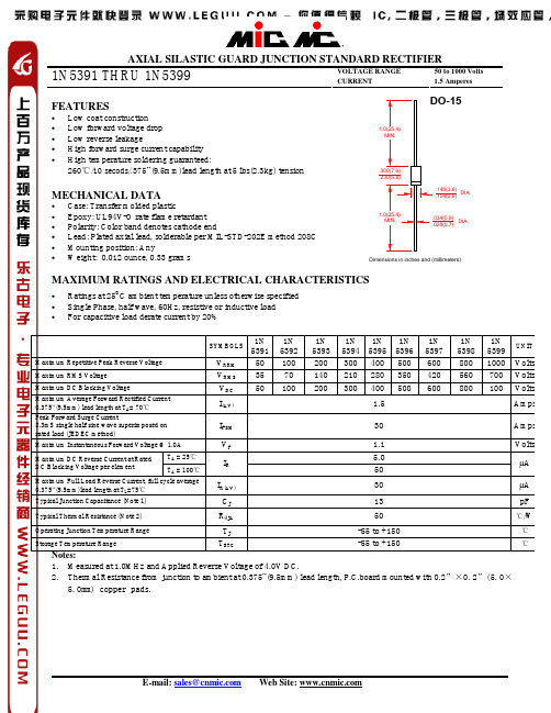
FEATURES• Low coat construction • Low forward voltage drop • Low reverse leakage• High forward surge current capability •High temperature soldering guaranteed:260℃/10 secods/.375”(9.5mm)lead length at 5 lbs(2.3kg) tensionMECHANICAL DATA• Case: Transfer molded plastic• Epoxy: UL94V-O rate flame retardant • Polarity: Color band denotes cathode end• Lead: Plated axial lead, solderable per MIL-STD-202E method 208C • Mounting position: Any•Weight: 0.012 ounce, 0.33 gramsMAXIMUM RATINGS AND ELECTRICAL CHARACTERISTICS• Ratings at 25O C ambient temperature unless otherwise specified • Single Phase, half wave, 60Hz, resistive or inductive load •For capacitive load derate current by 20%SYMBOLS1N 5391 1N 5392 1N5393 1N 5394 1N 5395 1N 5396 1N 5397 1N 5398 1N5399UNITMaximum Repetitive Peak Reverse Voltage V RRM 50 100 200 300 400 500 600 800 1000 Volts Maximum RMS Voltage V RMS 35 70 140 210 280 350 420 560 700 Volts Maximum DC Blocking VoltageV DC 50 100 200 300 400 500 600 800 100 VoltsMaximum Average Forward Rectified Current 0.375”(9.5mm) lead length at T A = 70℃ I (AV) 1.5 Amps Peak Forward Surge Current8.3mS single half sine wave superimposed on rated load (JEDEC method)I FSM 30 Amps Maximum Instantaneous Forward Voltage @ 1.0A V F 1.1 Volts T A = 25℃ 5.0 Maximum DC Reverse Current at Rated DC Blocking Voltage per elementT A = 100℃I R 50 µA Maximum Full Load Reverse Current, full cycle average 0.375”(9.5mm)lead length at T L =75℃ I R(AV) 30 µA Typical Junction Capacitance (Note 1) C J 13 pFTypical Thermal Resistance (Note 2) R θJA 50℃/W Operating Junction Temperature Range T J -55 to +150 ℃Storage Temperature RangeT STG-55 to +150℃Notes:1. Measured at 1.0MHz and Applied Reverse Voltage of 4.0V DC.2. Thermal Resistance from junction to ambient at 0.375”(9.5mm) lead length, P.C.board mounted with 0.2”×0.2”(5.0×5.0mm) copper pads .DIA..034(0.9).028(0.7).140(3.6).104(2.6)1.0(25.4)MIN..300(7.6).230(5.8)1.0(25.4)MIN.DIA.DO-15Dimensions in inches and (millimeters)CURRENT 1.5 AmperesI N S T A N T A N E O U S R E V E R S E C U R R E N T ,I N S T A N T A N E O U S F O R W A R D C U R R E N T ,C A P A C I T A N C E ,(p F )TJ=25°C F=1MHzREVERSE VOLTAGE,(VOLTS)100.14.01.010.0FIG.5-TYPICAL JUNCTION CAPACITANCEINSTANTANEOUS FORWARD VOLTAGE,(V)10100(A )0.11Pulse Width=300us 1% Duty CycleT =25°C100PERCENT OF RATED PEAKREVERSE VOLTAGE,(%)(m A )0.010.11.0T =25°C AMBIENT TEMPERATURE, (°C)FORWARD CHARACTERISTICSFIG.3-TYPICAL INSTANTANEOUS(A )A V E R A G E F O R W A R D C U R R E N T ,25Resistive orHalf Wave 60Hz Inductive LoadSingle Phase 0050125FIG.1-TYPICAL FORWARD CURRENTDERATING CURVEFIG.4-TYPICAL REVERSE FORWARD SURGE CURRENT(JEDEC Method) =T 8.3ms Single Half Sine-Wave NUMBER OF CYCLES AT 60 Hz10P E A K F O R W A R D S U R G EC U R R E N T , (A )CHARACTERISTICST =100°C jmaxT FIG.2-MAXIMUM NON-REPETITIVE PEAK0.30.60.91.21.51.8102030405060RATING AND CHRACTERISTIC CURVES 1N539 Thur 1N5399。
protel99元件名称对照表
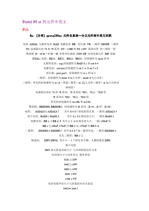
Protel 99 se的元件中英文PcbRe: [分享] protel99se 元件名系表--分立元件库中英文对照电阻AXIAL 无极性电容RAD 电解电容RB- 电位器VR 二极管DIODE 三极管TO 电源稳压块78和79系列TO-126H和TO-126V 场效应管和三极管一样整流桥D-44 D-37 D-46 单排多针插座CON SIP双列直插元件DIP晶振XTAL1电阻:RES1,RES2,RES3,RES4;封装属性为axial系列无极性电容:cap;封装属性为RAD-0.1到rad-0.4电解电容:electroi;封装属性为rb.2/.4到rb.5/1.0电位器:pot1,pot2;封装属性为vr-1到vr-5二极管:封装属性为diode-0.4(小功率)diode-0.7(大功率)三极管:常见的封装属性为to-18(普通三极管)to-22(大功率三极管)to-3(大功率达林顿管)电源稳压块有78和79系列;78系列如7805,7812,7820等79系列有7905,7912,7920等常见的封装属性有to126h和to126v整流桥:BRIDGE1,BRIDGE2: 封装属性为D系列(D-44,D-37,D-46)电阻:AXIAL0.3-AXIAL0.7其中0.4-0.7指电阻的长度,一般用AXIAL0.4 瓷片电容:RAD0.1-RAD0.3。
其中0.1-0.3指电容大小,一般用RAD0.1 电解电容:RB.1/.2-RB.4/.8 其中.1/.2-.4/.8指电容大小。
一般<100uF用RB.1/.2,100uF-470uF用RB.2/.4,>470uF用RB.3/.6 二极管:DIODE0.4-DIODE0.7 其中0.4-0.7指二极管长短,一般用DIODE0.4发光二极管:RB.1/.2集成块:DIP8-DIP40, 其中8-40指有多少脚,8脚的就是DIP8贴片电阻0603表示的是封装尺寸与具体阻值没有关系但封装尺寸与功率有关通常来说0201 1/20W0402 1/16W0603 1/10W0805 1/8W1206 1/4W电容电阻外形尺寸与封装的对应关系是:0402=1.0x0.50603=1.6x0.80805=2.0x1.21206=3.2x1.61210=3.2x2.51812=4.5x3.22225=5.6x6.5关于零件封装我们在前面说过,除了DEVICE。
proteus元件名称对照表
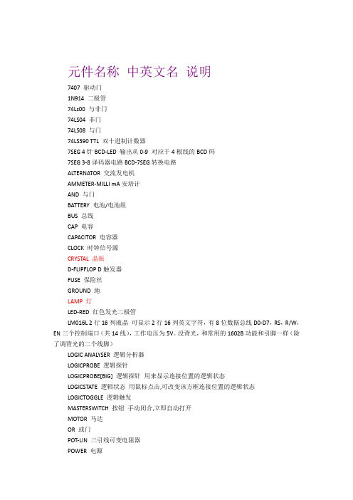
元件名称中英文名说明7407 驱动门1N914 二极管74Ls00 与非门74LS04 非门74LS08 与门74LS390 TTL 双十进制计数器7SEG 4针BCD-LED 输出从0-9 对应于4根线的BCD码7SEG 3-8译码器电路BCD-7SEG转换电路ALTERNATOR 交流发电机AMMETER-MILLI mA安培计AND 与门BATTERY 电池/电池组BUS 总线CAP 电容CAPACITOR 电容器CLOCK 时钟信号源CRYSTAL 晶振D-FLIPFLOP D触发器FUSE 保险丝GROUND 地LAMP 灯LED-RED 红色发光二极管LM016L 2行16列液晶可显示2行16列英文字符,有8位数据总线D0-D7,RS,R/W,EN三个控制端口(共14线),工作电压为5V。
没背光,和常用的1602B功能和引脚一样(除了调背光的二个线脚)LOGIC ANALYSER 逻辑分析器LOGICPROBE 逻辑探针LOGICPROBE[BIG] 逻辑探针用来显示连接位置的逻辑状态LOGICSTATE 逻辑状态用鼠标点击,可改变该方框连接位置的逻辑状态LOGICTOGGLE 逻辑触发MASTERSWITCH 按钮手动闭合,立即自动打开MOTOR 马达OR 或门POT-LIN 三引线可变电阻器POWER 电源RES 电阻PESPACK 排阻RESISTOR 电阻器SWITCH 按钮手动按一下一个状态SW-SPDT-mom 二选通一按钮触发开关BUTTONVOLTMETER 伏特计VOLTMETER-MILLI mV伏特计VTERM 串行口终端Electromechanical 电机Inductors 变压器Laplace Primitives 拉普拉斯变换Memory IcsMicroprocessor IcsMiscellaneous 各种器件AERIAL-天线;ATAHDD;ATMEGA64;BATTERY;CELL;CRYSTAL-晶振;FUSE;METER-仪表;Modelling Primitives 各种仿真器件是典型的基本元器模拟,不表示具体型号,只用于仿真,没有PCBOptoelectronics 各种发光器件发光二极管,LED,液晶等等PLDs & FPGAsResistors 各种电阻Simulator Primitives 常用的器件Speakers & SoundersSwitches & Relays 开关,继电器,键盘BUTTON 触发开关Switching Devices 晶阊管Transistors 晶体管(三极管,场效应管)TTL 74 seriesTTL 74ALS seriesTTL 74AS seriesTTL 74F seriesTTL 74HC seriesTTL 74HCT seriesTTL 74LS seriesTTL 74S seriesAnalog Ics 模拟电路集成芯片Capacitors 电容集合CMOS 4000 seriesConnectors 排座,排插Data Converters ADC,DACDebugging Tools 调试工具7SEG 数码管ECL 10000 Series 各种常用集成电路1.电阻2.固定电阻:RES3.半导体电阻:RESSEMT4.电位计;POT5.变电阻;RVAR6.可调电阻;res17.可变电阻pot8.2.电容9.定值无极性电容;CAP10.定值有极性电容;CAP11.半导体电容:CAPSEMI12.可调电容:CAPVARA700D3.电感:INDUCTOR4.二极管:发光二极管:LED5.三极管:NPN16.结型场效应管:场效应管场效应管9.继电器:PELAY. LIB10.灯泡:LAMP11.运放:OPAMP12.数码管:7-SEG_DP (MISCELLANEOUS13.开关;sw_pb原理图常用库文件:MiscellaneousDallasIntelProtel DOS SchematicPCB元件常用库:General部分分立元件库元件名称及中英对照AND 与门ANTENNA 天线BATTERY 直流电源BELL 铃,钟BVC 同轴电缆接插件BRIDEG 1 整流桥(二极管)BRIDEG 2 整流桥(集成块)BUFFER 缓冲器BUZZER 蜂鸣器CAP 电容CAPACITOR 电容CAPACITOR POL 有极性电容CAPVAR 可调电容CIRCUIT BREAKER 熔断丝COAX 同轴电缆CON 插口CRYSTAL 晶体整荡器DB 并行插口DIODE 二极管DIODE SCHOTTKY 稳压二极管DIODE VARACTOR 变容二极管DPY_3-SEG 3段LEDDPY_7-SEG 7段LEDDPY_7-SEG_DP 7段LED(带小数点) ELECTRO电解电容FUSE 熔断器INDUCTOR 电感INDUCTOR IRON 带铁芯电感INDUCTOR3 可调电感JFET N N沟道场效应管JFET P P沟道场效应管LAMP 灯泡LAMP NEDN 起辉器LED 发光二极管METER 仪表MICROPHONE 麦克风MOSFET MOS管MOTOR AC 交流电机MOTOR SERVO 伺服电机NAND 与非门NOR 或非门NOT 非门NPN NPN三极管NPN-PHOTO 感光三极管OPAMP 运放OR 或门PHOTO 感光二极管PNP 三极管NPN DAR NPN三极管PNP DAR PNP三极管POT 滑线变阻器PELAY-DPDT 双刀双掷继电器电阻可变电阻RESISTOR BRIDGE 桥式电阻RESPACK 电阻SCR 晶闸管PLUG 插头PLUG AC FEMALE 三相交流插头SOCKET 插座SOURCE CURRENT 电流源SOURCE VOLTAGE 电压源SPEAKER扬声器SW 开关SW-DPDY 双刀双掷开关SW-SPST 单刀单掷开关SW-PB 按钮THERMISTOR 电热调节器TRANS1 变压器TRANS2 可调变压器TRIAC 三端双向可控硅TRIODE 三极真空管VARISTOR 变阻器ZENER 齐纳二极管DPY_7-SEG_DP 数码管SW-PB 开关其他元件库Protel Dos Schematic 4000 Cmos .Lib (40.系列CMOS管集成块元件库)4013 D 触发器4027 JK 触发器Protel Dos Schematic Analog (模拟数字式集成块元件库)AD系列DAC系列HD系列MC系列Protel Dos Schematic (比较放大器元件库)Protel Dos Shcematic (INTEL公司生产的80系列CPU集成块元件库)Protel Dos Schematic (线性元件库)例555Protel Dos Schemattic Memory (内存存储器元件库)Protel Dos Schematic (SY系列集成块元件库)Protes Dos Schematic (摩托罗拉公司生产的元件库)Protes Dos Schematic (NEC公司生产的集成块元件库)Protes Dos Schematic Operationel (运算放大器元件库)Protes Dos Schematic (晶体管集成块元件库74系列)Protel Dos Schematic Voltage (电压调整集成块元件库)Protes Dos Schematic (齐格格公司生产的Z80系列CPU集成块元件库)元件属性对话框中英文对照Lib ref 元件名称Footprint 器件封装Designator 元件称号Part 器件类别或标示值Schematic Tools 主工具栏Writing Tools 连线工具栏Drawing Tools 绘图工具栏稳压二极管ZENER DIODE肖特基二极管SCHOTTKY DIODE二极管DIODE变容二极管VARIODE三极管TRANSISTOR电感INDUCTOR磁环EMIFIL电阻RESISTOR电容CAPACITY晶振CRYSTAL涤纶电容MYLAR CAP电解电容ELECT CAP瓷片电容CERAMIC CAP安规电容FILM CAPProtel 99 se的元件中英文PcbRe: [分享] protel99se 元件名系表--分立元件库中英文对照电阻AXIAL 无极性电容RAD 电解电容RB- 电位器VR 二极管DIODE 三极管TO 电源稳压块78和79系列TO-126H和TO-126V 场效应管和三极管一样整流桥D-44 D-37 D-46 单排多针插座CON SIP 双列直插元件DIP 晶振XTAL1电阻:RES1,RES2,RES3,RES4;封装属性为axial系列无极性电容:cap;封装属性为到电解电容:electroi;封装属性为.4到电位器:pot1,pot2;封装属性为vr-1到vr-5二极管:封装属性为(小功率)(大功率)三极管:常见的封装属性为to-18(普通三极管)to-22(大功率三极管)to-3(大功率达林顿管)电源稳压块有78和79系列;78系列如7805,7812,7820等79系列有7905,7912,7920等常见的封装属性有to126h和to126v整流桥:BRIDGE1,BRIDGE2: 封装属性为D系列(D-44,D-37,D-46)电阻:其中指电阻的长度,一般用瓷片电容:。
1N5391GP-E354;1N5393GP-E354;1N5395GP-E354;1N5397GP-E354;1N5398GP-E354;中文规格书,Datasheet资料
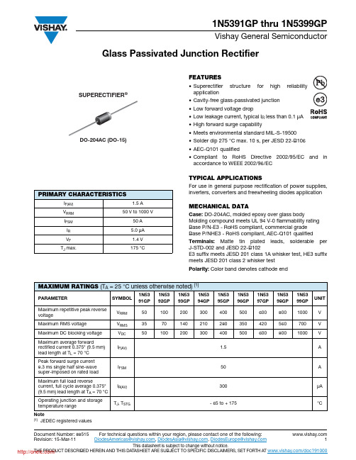
Document Number: 88515For technical questions within your region, please contact one of the following: Revision: 15-Mar-11DiodesAmericas@ , DiodesAsia@ , DiodesEurope@ 1This datasheet is subject to change without notice.THE PRODUCT DESCRIBED HEREIN AND THIS DATASHEET ARE SUBJECT TO SPECIFIC DISCLAIMERS, SET FORTH AT /doc?91000Glass Passivated Junction Rectifier1N5391GP thru 1N5399GPVishay General SemiconductorFEATURES•Superectifier structure for high reliability application•Cavity-free glass-passivated junction •Low forward voltage drop•Low leakage current, typical I R less than 0.1 μA •High forward surge capability•Meets environmental standard MIL-S-19500•Solder dip 275 °C max. 10 s, per JESD 22-B106•AEC-Q101 qualified•Compliant to RoH S Directive 2002/95/EC and in accordance to WEEE 2002/96/ECTYPICAL APPLICATIONSFor use in general purpose rectification of power supplies,inverters, converters and freewheeling diodes applicationMECHANICAL DATACase: DO-204AC, molded epoxy over glass bodyMolding compound meets UL 94 V-0 flammability rating Base P/N-E3 - RoHS compliant, commercial grade Base P/NHE3 - RoHS compliant, AEC-Q101 qualified Terminals: Matte tin plated leads, solderable per J-STD-002 and JESD 22-B102E3 suffix meets JESD 201 class 1A whisker test, HE3 suffix meets JESD 201 class 2 whisker test Polarity: Color band denotes cathode endNote(1)JEDEC registered valuesPRIMARY CHARACTERISTICSI F(AV) 1.5 A V RRM 50 V to 1000 VI FSM 50 A I R 5.0 μA V F 1.4 V T J max.175 °CDO-204AC (DO-15)SUPERECTIFIER ®MAXIMUM RATINGS (T A = 25°C unless otherwise noted) (1)ARAMETER SYMBOL 1N5391GP 1N5392GP 1N5393GP 1N5394GP 1N5395GP 1N5396GP 1N5397GP 1N5398GP 1N5399GP UNIT Maximum repetitive peak reverse voltageV RRM 501002003004005006008001000V Maximum RMS voltage V RMS 3570140210280350420560700V Maximum DC blocking voltage V DC 501002003004005006008001000V Maximum average forwardrectified current 0.375" (9.5 mm) lead length at T L = 70 °C I F(AV)1.5APeak forward surge current 8.3 ms single half sine-wave super-imposed on rated load I FSM50AMaximum full load reversecurrent, full cycle average 0.375" (9.5 mm) lead length at T A = 70 °C I R(AV)300μAOperating junction and storage temperature range T J , T STG- 65 to + 175°C/ For technical questions within your region, please contact one of the following:Document Number: 885152DiodesAmericas@ , DiodesAsia@ , DiodesEurope@ Revision: 15-Mar-11This datasheet is subject to change without notice.THE PRODUCT DESCRIBED HEREIN AND THIS DATASHEET ARE SUBJECT TO SPECIFIC DISCLAIMERS, SET FORTH AT /doc?910001N5391GP thru 1N5399GPVishay General SemiconductorNote(1)JEDEC registered valuesNote(1)Thermal resistance from junction to ambient at 0.375" (9.5 mm) lead length, P.C.B. mountedNote(1)AEC-Q101 qualifiedRATINGS AND CHARACTERISTICS CURVES(T A = 25 °C unless otherwise noted)Fig. 1 - Forward Current Derating CurveFig. 2 - Maximum Non-repetitive Peak Forward Surge CurrentELECTRICAL CHARACTERISTICS (T A = 25°C unless otherwise noted)P ARAMETER TEST CONDITIONSSYMBOL1N5391GP1N5392GP1N5393GP1N5394GP1N5395GP 1N5396GP1N5397GP1N5398GP1N5399GPUNITMaximuminstantaneous forward voltage 1.5 AT A = 70 °C V F (1)1.4VMaximum DC reverse current at rated DC blocking voltageT A = 25 °C I R (1) 5.0μAT A = 150 °C300Typical reverse recovery time I F = 0.5 A, I R = 1.0 A, I rr = 0.25 A t rr 2.0μs Typical junction capacitance4.0 V, 1 MHzC J15pFTHERMAL CHARACTERISTICS (T A = 25°C unless otherwise noted)PARAMETERSYMBOL 1N5391GP1N5392GP1N5393GP1N5394GP1N5395GP 1N5396GP1N5397GP1N5398GP1N5399GPUNITTypical thermal resistanceR JA(1)45°C/WORDERING INFORMATION (Example)PREFERRED P/N UNIT WEIGHT (g)PREFERRED PACKAGE CODEBASE QUANTITYDELIVERY MODE1N5397GP-E3/540.42554400013" diameter paper tape and reel1N5397GP-E3/730.425732000Ammo pack packaging 1N5397GPHE3/54 (1)0.42554400013" diameter paper tape and reel1N5397GPHE3/73 (1)0.425732000Ammo pack packaging/Document Number: 88515For technical questions within your region, please contact one of the following: Revision: 15-Mar-11DiodesAmericas@ , DiodesAsia@ , DiodesEurope@ 3This datasheet is subject to change without notice.THE PRODUCT DESCRIBED HEREIN AND THIS DATASHEET ARE SUBJECT TO SPECIFIC DISCLAIMERS, SET FORTH AT /doc?910001N5391GP thru 1N5399GPVishay General SemiconductorFig. 3 - Typical Instantaneous Forward Characteristics Fig. 4 - Typical Reverse Characteristics Fig. 5 - Typical Junction CapacitanceFig. 6 - Typical Transient Thermal ImpedancePACKAGE OUTLINE DIMENSIONS/Legal Disclaimer Notice VishayDisclaimerALL PRODU CT, PRODU CT SPECIFICATIONS AND DATA ARE SU BJECT TO CHANGE WITHOU T NOTICE TO IMPROVE RELIABILITY, FUNCTION OR DESIGN OR OTHERWISE.Vishay Intertechnology, Inc., its affiliates, agents, and employees, and all persons acting on its or their behalf (collectively,“Vishay”), disclaim any and all liability for any errors, inaccuracies or incompleteness contained in any datasheet or in any other disclosure relating to any product.Vishay makes no warranty, representation or guarantee regarding the suitability of the products for any particular purpose or the continuing production of any product. To the maximum extent permitted by applicable law, Vishay disclaims (i) any and all liability arising out of the application or use of any product, (ii) any and all liability, including without limitation special, consequential or incidental damages, and (iii) any and all implied warranties, including warranties of fitness for particular purpose, non-infringement and merchantability.Statements regarding the suitability of products for certain types of applications are based on Vishay’s knowledge of typical requirements that are often placed on Vishay products in generic applications. Such statements are not binding statements about the suitability of products for a particular application. It is the customer’s responsibility to validate that a particular product with the properties described in the product specification is suitable for use in a particular application. Parameters provided in datasheets and/or specifications may vary in different applications and performance may vary over time. All operating parameters, including typical parameters, must be validated for each customer application by the customer’s technical experts. Product specifications do not expand or otherwise modify Vishay’s terms and conditions of purchase, including but not limited to the warranty expressed therein.Except as expressly indicated in writing, Vishay products are not designed for use in medical, life-saving, or life-sustaining applications or for any other application in which the failure of the Vishay product could result in personal injury or death.Customers using or selling Vishay products not expressly indicated for use in such applications do so at their own risk and agree to fully indemnify and hold Vishay and its distributors harmless from and against any and all claims, liabilities, expenses and damages arising or resulting in connection with such use or sale, including attorneys fees, even if such claim alleges that Vishay or its distributor was negligent regarding the design or manufacture of the part. Please contact authorized Vishay personnel to obtain written terms and conditions regarding products designed for such applications.No license, express or implied, by estoppel or otherwise, to any intellectual property rights is granted by this document or by any conduct of Vishay. Product names and markings noted herein may be trademarks of their respective owners.Material Category PolicyVishay Intertechnology, Inc. hereb y certifies that all its products that are identified as RoHS-Compliant fulfill the definitions and restrictions defined under Directive 2011/65/EU of The European Parliament and of the Council of June 8, 2011 on the restriction of the use of certain hazardous substances in electrical and electronic equipment (EEE) - recast, unless otherwise specified as non-compliant.Please note that some Vishay documentation may still make reference to RoHS Directive 2002/95/EC. We confirm that all the products identified as being compliant to Directive 2002/95/EC conform to Directive 2011/65/EU.Revision: 12-Mar-121Document Number: 91000 /分销商库存信息:VISHAY-GENERAL-SEMICONDUCTOR1N5391GP-E3/541N5393GP-E3/541N5395GP-E3/54 1N5397GP-E3/541N5398GP-E3/541N5399GP-E3/54 1N5393GP-E3/731N5397GP-E3/731N5399GP-E3/73 1N5393GPHE3/731N5397GPHE3/731N5391GPHE3/54 1N5393GPHE3/541N5395GPHE3/541N5397GPHE3/54 1N5398GPHE3/541N5399GPHE3/731N5399GPHE3/54。
- 1、下载文档前请自行甄别文档内容的完整性,平台不提供额外的编辑、内容补充、找答案等附加服务。
- 2、"仅部分预览"的文档,不可在线预览部分如存在完整性等问题,可反馈申请退款(可完整预览的文档不适用该条件!)。
- 3、如文档侵犯您的权益,请联系客服反馈,我们会尽快为您处理(人工客服工作时间:9:00-18:30)。
1N5391THRU 1N5399
1.5 Amp Rectifier 50 - 1000 Volts
Features
• Low Leakage Current • High Current Capability
Maximum Ratings
•
Operating Temperature: -55°C to +150°C • Storage Temperature: -55°C to +150°C
• Typical Thermal Resistance; 26°C/W Junction To Lead
MCC Catalog Number
Device Marking
Maximum Recurrent Peak Reverse Voltage
Maximum RMS Voltage Maximum DC Blocking Voltage 1N5391 50V 35V 50V 1N5392 100V 70V 100V 1N5393 200V 140V 200V 1N5394 300V 210V 300V 1N5395 400V 280V 400V
1N5396 500V 350V 500V 1N5397 600V 420V 600V 1N5398 800V 560V 800V 1N5399 1000V 700V 1000V
Electrical Characteristics @ 25°C Unless Otherwise Specified
Average Forward Current
I F(AV)
1.5A
T A = 70°C
Peak Forward Surge Current I FSM 50A 8.3ms, half sine
Maximum Instantaneous Forward Voltage V F 1.1V
I FM = 1.5A;T J = 25°C Maximum DC
Reverse Current At Rated DC Blocking Voltage
I R
5.0µA 50µA T A = 25°C T A = 100°C Typical Junction Capacitance
C J
20pF
Measured at
1.0MHz, V R =4.0V
omp onents 20736 Marilla Street Chatsworth
! "# $ % ! "#
TM
Micro Commercial Components
• Case Material: Molded Plastic. UL Flammability Classification Rating 94V-0 and MSL rating 1
1N5391
1N53921N53931N53941N53951N5396
1N53991N53971N5398•
Lead Free Finish/RoHS Compliant (Note1) ("P"Suffix designates Compliant. See ordering information)
Note: 1. High Temperature Solder Exemption Applied, see EU Directive Annex 7.
元器件交易网
1N5391 thru 1N5399
Average Forward Rectified Current - Amperes
versus Ambient Temperature - °C
Figure 2
Forward Derating Curve
175
50
75
100125
0.25.5.75
Single Phase, Half Wave
60Hz Resistive or Inductive Load Amps
°C
150
1.01.25
1.5
Junction Capacitance - pF v ersus Reverse Voltage - Volts
Instantaneous Forward Current - Amperes versus Instantaneous Forward Voltage - Volts
Figure 1
Typical Forward Characteristics 462010Amps
.4
.6
.8 1.0
1.2
1.4
.01
.02.04.06.1.2
.4.612
25°C
Volts
Figure 3
Junction Capacitance
.1
.2
1.4
2
10
20
40
4
100
200
1261020100pF
Volts
60404400
1000
T J =25°C
TM
Micro Commercial Components
1N5391 thru 1N5399
1
100
4
0102030
8Figure 4
Peak Forward Surge Current Peak Forward Surge Current - Amperes versus
Number Of Cycles At 60Hz - Cycles
Amps
Cycles
2
6
1020
608040
405060TM
Micro Commercial Components
Micro Commercial Components
Ordering Information
Device Packing (Part Number)-TP Tape&Reel;4Kpcs/Reel
(Part Number)-BP Bulk;500pcs/Box
***IMPORTANT NOTICE***
Micro Commercial Components Corp . reserve s the right to make changes without further notice to any
product herein to make corrections, modifications , enhancements , improvements , or other changes .
Micro Commercial Components Corp.does not assume any liability arising out of the application or
use of any product described herein; neither does it convey any license under its patent rights ,nor
the rights of others . The user of products in such applications shall assume all risks of such use
and will agree to hold Micro Commercial Components Corp.and all the companies whose
products are represented on our website, harmless against all damages.
***APPLICATIONS DISCLAIMER***
Products offer by Micro Commercial Components Corp.are not intended for use in Medical,
Aerospace or Military Applications.。
