95-21UYC-S530-A5-TR10 亿光LED规格书
优波光电技术有限公司 LED 产品说明书

■Features■Outline Dimension●Top view white LED (3.0 x 1.4 x 0.8mm)● Super high brightness of surface mount LED ● Lead frame package with individual 2 pins●Compatible to IR reflow soldering.■Applications●General lighting ●Decoration lighting●Indicator2, Anode 1, CathodeUnit:mmTolerances: ±0.1mm21Top ViewBack ViewSide View■Absolute Maximum Rating (Ta=25℃)■DirectivityItemSymbolValue UnitDC Forward Current I F 30 mA Pulse Forward Current* I FP 100mA Reverse V oltage V R 5 V Power Dissipation P D 110 mWOperating Temperature Topr -40 ~ +85 ℃ Storage Temperature Tstg -40~ +85 ℃Lead Soldering TemperatureTsol260℃/5sec-*Pulse width Max 0.1ms, Duty ratio max 1/10■Electrical -Optical Characteristics(Ta=25(Ta=25℃℃)V F (V)I R (µA) Iv(mcd)CCT2θ1/2(deg)Min. Typ. Max. Max. Min.Typ. Max.Min. Typ. Max. Typ.Part NumberColorI F =20mAV R =5V I F =20mAOSW33014C1AWhiteW ■2.93.1 3.6 10 2000 - 3000 5000K - 6000K 120 OSM53014C1A Warm White M ■2.93.13.6102000-3000 2800K-3500K120Note: * Vf tolerance: ±0.05V* Luminous flux measurement allowance is:±10%LED & Application Technologies■Rank* Correspondence Table of Luminous Flux – Intensity■Chromaticity DiagramLED & Application Technologies*Bin Range of Chromaticity Coordinates (OSW33014C1A)LED & Application TechnologiesCodeX1 Y1 X2 Y2 X3 Y3 X4 Y4 D06 0.3221 0.3523 0.3324 0.3612 0.3324 0.3520 0.3224 0.3420D09 0.3224 0.3430 0.3324 0.3520 0.3323 0.3429 0.3228 0.3336 D12 0.3228 0.3336 0.3323 0.3429 0.3323 0.3337 0.3231 0.3243 D15 0.3231 0.3243 0.3323 0.3337 0.3322 0.3245 0.3234 0.3149 E03 0.3324 0.3612 0.3470 0.3738 0.3461 0.3637 0.3324 0.3520 E05 0.3324 0.3520 0.3461 0.3637 0.3452 0.3536 0.3323 0.3429 E07 0.3323 0.3429 0.3452 0.3536 0.3442 0.3435 0.3323 0.3337 E090.33230.33370.34420.34350.34330.33340.33220.3245*Bin Range of Chromaticity Coordinates (OSM53014C1A)*If color binning is required, only one color group is allowed for each chip within a reel. Chromaticity coordinate groups are measured with an accuracy of ±0.01 *Color coordinate is derived from the CIE 1931 chromaticity.*Bin rank of VFWhiteRank (I F =20mA)88T-999 AAA BBB DC Forward Voltage(v)2.9-3.23.2-3.43.4-3.6*Forward voltage is measured with an accuracy of ±0.1V.LED & Application TechnologiesCodeX1 Y1 X2 Y2 X3 Y3 X4 Y4 G04 0.4160 0.4199 0.4373 0.4302 0.4313 0.4166 0.4112 0.4067G06 0.4112 0.4067 0.4313 0.4166 0.4252 0.4030 0.4063 0.3936 G08 0.4063 0.3936 0.4252 0.4030 0.4192 0.3893 0.4015 0.3804 G10 0.4015 0.3804 0.4192 0.3893 0.4131 0.3757 0.3966 0.3672 H04 0.4373 0.4302 0.4518 0.4354 0.4453 0.4216 0.4313 0.4166 H05 0.4518 0.4354 0.4689 0.4408 0.4614 0.4265 0.4453 0.4216 H07 0.4313 0.4166 0.4453 0.4216 0.4387 0.4077 0.4252 0.4030 H08 0.4453 0.4216 0.4614 0.4265 0.4539 0.4123 0.4387 0.4077 H10 0.4252 0.4030 0.4387 0.4077 0.4322 0.3939 0.4192 0.3893 H11 0.4387 0.4077 0.4539 0.4123 0.4463 0.3980 0.4322 0.3939 H13 0.4192 0.3893 0.4322 0.3939 0.4256 0.3800 0.4131 0.3757 H14 0.43220.39390.44630.39800.43880.38370.42560.3800■Typical Electro-Optical Characteristics CurvesLED & Application TechnologiesRELIABILITY TEST REPORTCLASSIFICATIONTEST TIME TEST CONDTION OPERATION LIFE If:20mA Ta:25+5TEST ITME=1000HRS(-24HRS,+72HRS) HIGHTEMPERTURE HIGH HUMIDITYSTORAGER.H:90~95% Ta:65+5℃TEST ITME=240HRS(+2HRS)HIGH TEMPERTURE STORAGETa:105+5℃TEST ITME=500HRS(-24HRS,+48HRS) ENDURANCE TESTLOWTEMPERTURESTORAGETa:-55+5℃TEST ITME=500HRS(-24HRS,+48HRS) TEMPERTURE CYCLING105℃~25℃~-55℃~25℃ 60min 10min 60min 10min 20cyclesTHERMAL SHOCK105℃~-55℃ 10min 10min 10cyclesSOLDER RESISTANCE Ta:260+5℃ TEST ITME=10+1sec ENVIRONMENTAL TESTSOLDERABILITYTa:230+5℃TEST ITME=5+1secJUDGMENT CRITERIA OF FALURE FOR THE RELIABILITYMEASURING ITMESYMBOLCONDITIONSFAILUERLUMINOUS INTENSITY IV IF=20mA IV<0.5*INITIALV ALUEFORWARD VOLTAGEVFIF=20mA VF>1.2*INITIALV ALUEREVERSE CURRENT IR Vr=5V IR>2*SPECLED & Application Technologies■Recommended Reflow Soldering ProfileSurface mounting conditionIn automatic mounting of the SMD LEDs on printed circuit boards, any bending, expanding and pulling forces or shock against the SMD LEDs should be kept min. to prevent them from electrical failures and mechanical damages of the devices.Soldering reflow-Soldering of the SMD LEDs should conform to the soldering condition in the individual specifications. -SMD LEDs are designed for reflow soldering.-In the reflow soldering, too high temperature and too large temperature gradient such as rapid heating/cooling may cause electrical & optical failures and damages of the devices.-Wellypower can’t guarantee the LEDs after they have been assembled using the solder dipping method.LED & Application Technologies3) Manual soldering.- Lead solderMax. 300℃for max. 3sec, and only one time. - Lead-free solderMax. 350℃for max. 3sec, and only one time.- There is possibility that the brightness of LEDs is decreased, which is influenced by heat or ambient atmosphere during reflow. It is recommended to use the nitrogen reflow method use the nitrogen reflow method.- After LEDs have been soldered, repairs should not be done. As repair is unavoidable, a doublehead soldering iron should be used. It should be confirmed beforehand whether the characteristics of the LEDs will be damaged by repairing or not.- Reflow soldering should not be done more than two times.LED & Application Technologies■Package ModelLoaded Quantity 4000 pcs. Per ReelReel PartLED & Application Technologies。
LED日光灯管规格书及灯头型号..

LED日光灯管规格书LED日光灯管规格书型号包括:T4、T5、T8、T9、T10等,表示灯管粗细。
简单地:T后面的数值,表示灯管周长,例如T4的周长为4厘米、T5的周长为5厘米。
算成直径:T8的直径是1英寸(2.54厘米),T4的直径是0.5英寸(1.27厘米),….。
T代表灯管的直径1T=1/8″1″=25.4mm1T=3.175mmT4=12.7mmT5=16mmT8=25.4mmT9=28.6mmT10=31.8mm注:日光灯的灯头主要用G5、G13的企业用的三支灯管一组的通常是T5的灯管,很早以前常用的日光灯规格书有T10、T12。
“T”,代表“Tube”,表示管状的,T后面的数字表示灯管直径。
T8就是有8个“T”,一个“T”就是1/8英寸。
一英寸等于25.4毫米。
那么每一个“T”就是25.4÷8=3.175mmT12灯管的直径规格书就是(12/8)×25.4=38.1 mmT10灯管的直径规格书就是(10/8)×25.4=31.8mmT8灯管的直径规格书就是(8/8)×25.4=25.4mm [T8的刚好是直径一英寸的灯管] (注:统一宽度39mm、高度52mm)常用的日光灯长度与功率:(20w 长620mm; 30w 长926mm; 40w长1230mm) T5灯管的直径就是(5/8)×25.4=16 mm (注:统一宽度23.5mm、高度39mm)常用的日光灯长度与功率:(8w 长310mm; 14w 长570mm; 21w 长870.5mm; 28w 长1170.5mm; 35w 长1475mm)T4灯管的直径就是(4/8)×25.4=12.7 mm (注:统一宽度21mm、高度32mm)常用的日光灯长度规格书与功率:(8w 长341mm; 12w 长443mm; 16w 长487mm; 20w 长534mm;22w 长734mm; 24w 长874mm; 26w 长1025mm; 28w 长1172mm)T3.5灯管的直径就是(3.5/8)×25.4=11.1 mmT2灯管的直径就是(2/8)×25.4=6.4 mmLed日光灯管规格书是依照普通日光灯规格书制造的,其规格大至相同,可以不更换支架的前提下方便地将LED日光灯替换普通日光灯以达到环保节能,有利于节省更换的成本。
亿光3535灯珠规格书
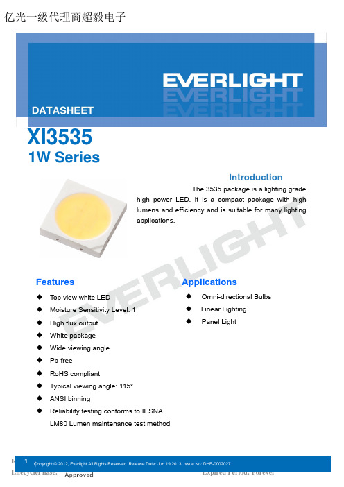
IntroductionThe 3535 package is a lighting gradehigh power LED.It is a compact package with high lumens and efficiency and is suitable for many lighting applications.FeaturesApplications◆Top view white LED ◆ Moisture Sensitivity Level: 1◆High flux output ◆White package ◆Wide viewing angle ◆Pb-free ◆RoHS compliant◆Typical viewing angle: 115°◆ANSI binning◆Reliability testing conforms to IESNA LM80 Lumen maintenance test method◆Omni-directional Bulbs ◆Linear Lighting ◆Panel LightXI35351W Series 亿光一级代理商超毅电子Table of ContentsProduct Nomenclature (3)Absolute Maximum Ratings (4)PN of the XI3535 series: Warm White LEDs (5)PN of the XI3535 series: Neutral White LEDs (6)PN of the XI3535 series: Cool White LEDs (7)Product Binning (8)Mechanical Dimension (16)Pad Configuration (16)Reflow Soldering Characteristics (18)Wavelength Characteristics (19)Typical Electrical Characteristics (19)Typical Relative Luminous Flux V.S. Forward Current (20)Typical Wavelength & Color Shift Characteristics (20)Typical Radiation Patterns (21)Emitter Tape Packaging (22)Emitter Reel Packaging (23)Product Labeling (23)Reliability Data (23)Storage Conditions (24)Revision History (26)Product NomenclatureThe product name is designated as below:XI3535– ABCDEFG–HIJKL–MNOPDesignation:AB = color [1]CD = color bin or CCT bin[1]E = Steps Mcadams binFG = min. luminous flux (lm) or radiation power (mW) performanceHI = forward voltage binJ = internal codeKL = power consumption[2]M = internal codeN = DamO = internal codeP =packaging type[3]Notes1.Table of color offerings:Color CCT range Color Rendering Index GT Cool-White4745~7050K>65KT Cool-White4745~7050K>80PT Cool-White4745~7050K>90HT Cool-White4745~7050K>93Warm-White2580~3710KLM>70Neutral-White3710K-4745KWarm White2580~3710K>80 KMNeutral-White3710K-4745KWarm White2580~3710K>90 PMNeutral-White3710K-4745KWarm White2580~3710K>93 HMNeutral-White3710K-4745K2.Table of power consumptions:Description011W3.Table of packaging types:DescriptionP TapeAbsolute Maximum RatingsMax. DC Forward Current (mA)IF350mA Max. Peak Pulse Current (mA)IPulse720mA Power Dissipation Pd1WThermal Resistance R th15°C/WOperating Temperature Topr-40 ~ +85°CStorage Temperature Tstg-40 ~ +100°CJunction temperature Tj115°C Max. Soldering Temperature T Sol260Notes:1.Maximum forward current for 1W is 350mA (Solder Pad=25°C).2.Duty cycle = 1/10@1KHZMin. LuminousFlux(lm)Typ.LuminousFlux(lm)CCT (K)Wavelength(nm)ForwardVoltage(V)ForwardCurrent(mA)CRI(Min.)XI3535-KM277F9-03201-000P9010027K-1,27K-227K-3,27K-42.95-3.8535080XI3535-KM307F9-03201-000P9010430K-1,30K-230K-3,30K-42.95-3.8535080XI3535-KM357F9-03201-000P9010535K-1,35K-235K-3,35K-42.95-3.8535080XI3535-HM307F8-03201-000P808430K-1,30K-230K-3,30K-42.95-3.8535093Notes:1.Luminous flux measurement tolerance: ±10%.2.The data of luminous flux measured at thermal pad=25°C3.Typical luminous flux or light output performance is operated within the condition guided by this datasheet4.The CRI value is based on the Everlight testing instrument.5.CRI measurement tolerance:±2.Min. LuminousFlux(lm)Typ.LuminousFlux(lm)CCT (K)Wavelength(nm)ForwardVoltage(V)ForwardCurrent(mA)CRI(Min.)XI3535-KM407F9-03201-000P9010740K-1,40K-240K-3,40K-42.95~3.8535080Notes:1.Luminous flux measurement tolerance: ±10%.2.The data of luminous flux measured at thermal pad=25°C3.Typical luminous flux or light output performance is operated within the condition guided by this datasheet4.The CRI value is based on the Everlight testing instrument.5.CRI measurement tolerance:±2.PN of the XI3535 series: Cool White LEDsMin. LuminousFlux(lm)Typ.LuminousFlux(lm)CCT (K)Wavelength(nm)ForwardVoltage(V)ForwardCurrent(mA)CRI(Min.)XI3535-KT507J1-03201-000P10011050K-1,50K-250K-3,50K-42.95-3.8535080XI3535-KT577J1-03201-000P10011157K-1,57K-257K-3,57K-42.95-3.8535080XI3535-KT607J1-03201-000P10010957K-2,57K-365K-1,65K-42.95-3.8535080XI3535-KT657J1-03201-000P10010865K-1,65K-265K-3,65K-42.95-3.8535080XI3535-PT577F9-03201-000P909757K-1,57K-257K-3,57K-42.95-3.8535090Notes:1.Luminous flux measurement tolerance: ±10%.2.The data of luminous flux measured at thermal pad=25°C3.Typical luminous flux or light output performance is operated within the condition guided by this datasheet4.The CRI value is based on the Everlight testing instrument.5.CRI measurement tolerance:±2.Product BinningLuminous Flux Bins14511001102562110120368312013048104130140510135140150613176150160717207160180820238180200E 92327J9200225127331225250233392250275339453275300445524300325552605325350660706350375770807375400880908400425F 990100K9425450White Bin StructureNotes:1.The CCT range of Cool-White varies from 4745K to 7050K.2.The CCT range of Neutral-White varies from 3710K to 4745K.3.The CCT range of Warm-White varies from 2580K to 3710K4.Color coordinates measurement allowance : ±0.015.Color bins are defined at I F =350mA operationCool-White Bin StructureChromaticity specification defined by ANSI亿光一级代理商超毅电子Cool-White Bin Coordinates5000K0.3460.3690.3380.3620.3450.3560.3370.3490.3530.3620.3450.35650K-10.3550.37650K-20.3460.369Reference Range: 4745~5000K Reference Range: 5000~5310K 0.3450.3560.3370.3490.3440.3430.3370.3370.3520.3490.3440.34350K-40.3530.36250K-30.3450.356Reference Range: 4745~5000K Reference Range: 5000~5310K 5700K0.3290.3540.3210.3460.3290.3420.3220.3350.3370.3490.3290.34257K-10.3380.36257K-20.3290.354Reference Range: 5310~5700K Reference Range: 5700~6020K CIE X CIE Y Bin CIE X CIE Y 0.3290.3420.3220.3350.3290.3310.3220.3240.3370.3370.3290.33157K-40.3370.34957K-30.3290.342Reference Range: 5310~5700K Reference Range: 5700~6020K 6000KCIE X CIE Y BinCIE X CIE Y 0.3210.3460.3120.3390.3220.3350.3130.3290.3290.3420.3210.33757K-20.3290.35465K-10.3210.348Reference Range: 5700~6020K Reference Range: 6020~6500K CIE X CIE Y Bin CIE X CIE Y 0.3220.3350.3130.3290.3220.3240.3150.3190.3290.3310.3220.32657K-30.3290.34265K-40.3210.337Reference Range: 5700~6020K Reference Range: 6020~6500K 6500KCIE X CIE Y BinCIE X CIE Y 0.3120.3390.3030.3300.3130.3290.3050.3210.3210.3370.3130.32965K-10.3210.34865K-20.3120.339Reference Range: 6020~6500K Reference Range: 6500~7050K 亿光一级代理商超毅电子0.3130.3290.3050.3210.3150.3190.3070.3110.3220.3260.3150.31965K-40.3210.33765K-30.3130.329Reference Range: 6020~6500KReference Range: 6500~7050KNote:1.Color coordinates measurement allowance : ±0.01.Neutral-White Bin StructureNeutral-White Bin Coordinates4000KCIE X CIE Y BinCIE X CIE Y 0.3870.3960.3740.3870.3830.3800.3700.3730.3950.3880.3830.38040K-10.4010.40440K-20.3870.396Reference Range: 3710~4000K Reference Range: 4000~4260K CIE X CIE Y Bin CIE X CIE Y 0.3830.3800.3700.3730.3780.3650.3670.3580.3900.3720.3780.36540K-40.3950.38840K-30.3830.380Reference Range: 3710~4000K Reference Range: 4000~4260K4500K0.3640.3810.3550.3740.3620.3660.3530.3600.3700.3730.3620.36645K-10.3740.38745K-20.3640.381Reference Range: 4260~4500K Reference Range: 4500~4745K 0.3620.3660.3530.3600.3590.3520.3510.3470.3670.3580.3590.35245K-40.3700.37345K-30.3620.366Reference Range: 4260~4500KReference Range: 4500~4745K Note:1.Color coordinates measurement allowance : ±0.01.Warm-White Bin StructureWarm-White Bin Coordinates2700KCIE X CIE Y BinCIE X CIE Y 0.469 0.429 0.4560.4260.459 0.4100.4470.4080.470 0.413 0.4590.41027K-10.481 0.43227K-20.4690.429Reference Range: 2580~2700K Reference Range: 2700~2870K CIE X CIE Y Bin CIE X CIE Y 0.459 0.410 0.447 0.408 0.448 0.3920.437 0.3890.459 0.394 0.448 0.392 27K-40.470 0.41327K-30.459 0.410Reference Range: 2580~2700K Reference Range: 2700~2870K 3000KCIE X CIE Y BinCIE X CIE Y 0.4430.4210.4300.4170.4350.4030.4220.3990.4470.4080.4350.40330K-10.4560.42630K-20.4430.421Reference Range: 2870~3000K Reference Range: 3000~3220K CIE X CIE Y Bin CIE X CIE Y 0.4350.4030.4220.3990.4260.3850.4150.3810.4370.3890.4260.38530K-40.4470.40830K-30.4350.403Reference Range: 2870~3000K Reference Range: 3000~3220K3500K0.4150.4090.4000.4020.4080.3920.3940.3850.4220.3990.4080.39235K-10.4300.41735K-20.4150.409Reference Range: 3220~3500K Reference Range: 3500~3710K 0.4080.3920.3940.3850.4020.3750.3890.3690.4150.3810.4020.37535K-40.4220.39935K-30.4080.392Reference Range: 3220~3500KReference Range: 3500~3710K Note:1.Color coordinates measurement allowance : ±0.01.Forward Voltage BinsV1 2.95 3.25V2 3.25 3.55V3 3.55 3.85Notes:1.Forward voltage measurement tolerance: ±0.1V.2.Forward voltage bins are defined at I F=350mA operation.Mechanical Dimension..4.2Notes:1.Dimensions are in millimeters.2.Tolerances unless mentioned are ±0.15mm.3.The thermal pad is electrically unity from the Anode and contact pads.4.Do not handle the device by the lens.Incorrect force applied to the lens may lead to the failure of devices.Pad ConfigurationTOP VIEW BOTTOM VIEWPAD FUNCTION1ANODE2CATHODEReflow Soldering CharacteristicsFor Reflow Processa.3535series are suitable for SMT processes.b.Curing of glue in oven must be according to standard operation flow processes.c.Reflow soldering should not be done more than twice.d.In soldering process, stress on the LEDs during heating should be avoided.e.After soldering, do not bend the circuit board.Wavelength CharacteristicsFor Cool-White,Warm-White Relative Spectral Distribution @ Solder Pad Temperature = 254005006007008000.00.20.40.60.81.0Warm-white-CRI>80 Nature-white-CRI>80 Cool-white-CRI>80 Warm-white-CRI>90 Cool-white-CRI>90R e l a t i v e L u m i n o u s I n t e n s t i yWavelength(nm)Typical Electrical CharacteristicsFor Cool-White,Warm-White @ Solder Pad Temperature = 25501001502002503003502.52.62.72.82.93.03.13.23.3F o r w a r d V o l t a g e (V )Forward Current(mA)Typical Relative Luminous Flux V.S. Forward CurrentFor Cool-White ,Warm-White @ Solder Pad Temperature = 250501001502002503003500.00.20.40.60.81.0R e l a t i v e L u m i n o u s I n t e n s i t yForward Current(mA)Typical Wavelength & Color Shift CharacteristicsV.S. Forward CurrentFor Cool-White , Warm-White @ Solder Pad Temperature = 2550100150200250300350200030004000500060007000Cool-White Warm-WhiteC C TForward Current(mA)Forward Current Derating Curve @ Junction Temperature <11520406080100100150200250300350400F o r w a r d C u r r e n t (m A )Soldering Temperature oCTypical Radiation Patterns3535 series:Typical Diagram Characteristics of Radiation for Warm-White andCool-White108090Notes:1.2θ1/2 is the off axis angle from lamp centerline where the luminous intensity is 1/2 of the peak value.2.View angle tolerance is ± 5∘.Emitter Tape Packaging MOQ>2Kpcs, multiple of 400pcs per reel,max 1600pcs MOQ <2Kpcs, multiple of 100pcs per reel,max 1600pcsEmitter Reel Packaging Reel DimensionsNotes:1.Dimensions are in millimeters.2.Tolerances unless mentioned are ±0.1mm.Product LabelingLabel ExplanationCPN: Customer Specification (when required)P/N : Everlight Production NumberQTY: Packing QuantityCAT: Luminous Flux (Brightness) BinHUE: Color BinREF: Forward Voltage BinLOT No: Lot NumberMADE IN TAIWAN: Production PlaceReliability DataReflow Tsol=260 , 10sec 3 timesThermal ShockH 100 20min.'∫ 10sec.'L 10 20min.500,1000 CyclesPower Temperature Cycle H 85 15min.'∫ 5min.'L 40 15min.IF=350mA500,1000 CyclesHigh Temperature/HumidityOperationTa=85 , RH=85%, IF=225mA1000hoursRoom Temperature OperationLifeTa=25 , IF=350mA1000hoursHigh Temperature OperationLife #1Ta=55 , IF=350mA1000hoursHigh Temperature OperationLife #2Ta=85 , IF=225mA1000hoursLow Temperature OperationLifeTa=-40 , IF=350mA1000hoursPulse 30ms ON/2500ms OFF / 30000 CyclesIF=720mA30ms ON/2500ms OFF /30000 CyclesFailure Criteria:1.LEDs are open or shorted2.lm: luminous flux attenuate difference(1000hrs)>50%3.VF: forward voltage difference(1000hrs)>20%Storage Conditions⏹Before the package is opened: The LEDs should be stored at 30°C or less and 50%RH or less after beingshipped from Everlight.The storage life is6 months. If the LEDs are to be stored for more than 6months, they should be stored in a sealed container with a nitrogen atmosphere and moisture absorbent material.⏹After opening the package: The LED's should be stored under 30 or less and 30%RH or less. The LEDshould be used within 168hrs (7days) after opening the package. If unused LEDs remain, they should be stored in moisture proof packages.⏹Before using LEDs: The LEDs should be baked under the following conditions: pre-curing at 60±5 for 24hours.⏹Do not stack assemblies containing Everlight XI3535 LEDs to prevent damage to the optical surface ofLEDs. Forces applied to the optical surface may result in the surface being damaged.Revision HistoryCurrent version: 06.19.2013Issue No:DHE-0002027Version: 10Created by: Betty HongP5,P6,P7New 3000K 4000K 5000K Series.2012-12-07 P7New XI3535-KT657J1-03201-000P2013-02-07 P4Change the Max. Peak Pulse Current2013-03-13 P5,P7Create New CRI>90 spec2013-03-26P21MOQ>2Kpcs, multiple of 400pcs per reelMOQ <2Kpcs, multiple of 100pcs per reel2013-04-09P23Create Reliability Data2013-04-18 P21Create Package Quantity max 1600pcs2013-05-28 P5,P7Added the 4000K and 6000K Color06-19-2013。
LED路灯产品规格书

含CRS-A-80W 和CRS-A-240W 两种型号。
表.2 A 系列高亮节能LED 路灯规格参数表名称A 系列高亮节能LED 路灯型号 CRS-A-80W CRS-A-240W 流明数 7200lm 21600lm 色温 6000K 6000K 亮点灯数 24 72 消耗功率 80W 240W 有效功率 95% 95% 适用场所 次干道 主干道 灯具高度 6米10米,12米 照明强度 25米长*6米宽/灯下30lux ,远端8lux 40米长*10米宽/灯下70lux ,远端8lux输入电压 交流/220V 点灯方式 恒定直流驱动.驱动模组 温度-30℃~+40℃, 驱动模组组合于灯具内或外外观结构 铝合金灯壳含鳍片一体成型 灯罩材质 透明,抗紫外线PC 材质产品制程 采用平板热超导散热技术,符合国际ROHS 环保规范 操作环境 无散热,风扇及冷凝器机制,操作结温67℃以下接头规格 符合3C 安全规范的电缆线 防尘防水 符合防水防尘IP65规范灯体寿命5万~10万小时应用范围:适用于高速公路、城市主干道及次干道、体育场、人行道、居住区、工业区、广场、公园、学校、别墅、庭院等场所的路灯照明。
或需要高品质照光的商场、剧院、高天井办公室和高屋顶工厂厂内之用。
CRS-A-80WCRS-A-240W包含18W、25W、100W a型、100W b型和150W高亮节能LED路灯。
➢B系列18W LED路灯18W LED路灯外观表.3 B系列18W高亮节能LED路灯规格参数名称B系列18W高亮节能LED路灯型号CRS-B-18W光源超高亮度节能LED路灯灯源光通量1,080lm路面光通量605lm输入电压12V 直流输入电流 1.75A 直流LED功率18W灯高照度照明范围3.5米22 lux 19米(Φ)4米17 lux 22米(Φ)5米11 lux 28米(Φ)6米8 lux 33米(Φ)工作环境-30℃~ +40 ℃防护等级全密封,>IP65灯具寿命5万~10万小时外观尺寸300×136×60mm重量3公斤应用范围:适用于城市道路、居住区、工业区、人行道、广场、公园、学校、别墅、庭院等场所照明。
亿光LED网规格书 17-21UYC-S530-XX-TR8
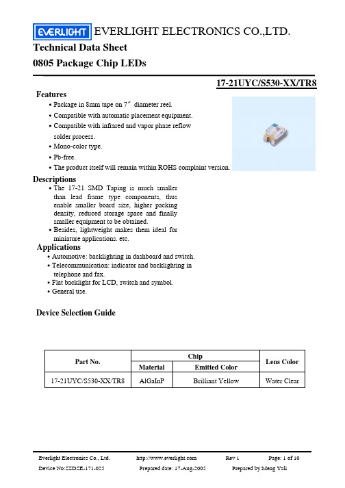
Technical Data Sheet0805 Package Chip LEDs17-21UYC/S530-XX/TR8 Features․Package in 8mm tape on 7〞diameter reel.․Compatible with automatic placement equipment.․Compatible with infrared and vapor phase reflowsolder process.․Mono-color type.․Pb-free.․The product itself will remain within ROHS complaint version.Descriptions․The 17-21 SMD Taping is much smallerthan lead frame type components, thusenable smaller board size, higher packingdensity, reduced storage space and finallysmaller equipment to be obtained.․Besides, lightweight makes them ideal forminiature applications. etc.Applications․Automotive: backlighting in dashboard and switch.․Telecommunication: indicator and backlighting intelephone and fax.․Flat backlight for LCD, switch and symbol.․General use.Device Selection GuideChipLens Color Part No.ColorMaterial Emitted17-21UYC/S530-XX/TR8 AlGaInP Brilliant Yellow Water Clear17-21UYC/S530-XX/TR8 Package Outline DimensionsNote: The tolerances unless mentioned is ±0.1mm ,Unit = mm17-21UYC/S530-XX/TR8 Absolute Maximum Ratings (Ta=25℃)Parameter Symbol Rating UnitReverse Voltage V R 5 VForward Current I F 25 mA Operating Temperature Topr -40 ~ +85 ℃Storage Temperature Tstg -40~ +90 ℃ElectrostaticDischarge(HBM)ESD 2000 VPower Dissipation Pd 60 mWPeak Forward Current(Duty 1/10 @1KHz)I FP 60 mASoldering Temperature Tsol Reflow Soldering : 260 ℃for 10 sec. Hand Soldering : 350 ℃for 3 sec.17-21UYC/S530-XX/TR8Electro-Optical Characteristics (Ta=25℃)Parameter Symbol*ChipRankMin. Typ. Max. UnitConditionA2 15 38 ----- A3 40 62----- A4 50 75 -----A5 60 96----- A6 85 124 ----- Luminous IntensityIvA7 110 146----- mcdViewing Angle 2θ1/2 ----- ----- 140 ----- deg Peak Wavelength λp ----- ----- 591 ----- nm Dominant Wavelength λd ----- ----- 589 ----- nm Spectrum RadiationBandwidth △λ ----- -----15 -----nm Forward Voltage V F ----- 1.7 2.0 2.4 V I F =20 mAReverse CurrentI R---------- ----- 10μAV R =5V*17-21UYC/S530-XX/TR8Chip Rank17-21UYC/S530-XX/TR8Reel DimensionsNote: The tolerances unless mentioned is ±0.1mm ,Unit = mm17-21UYC/S530-XX/TR8 Carrier Tape Dimensions: Loaded quantity 3000 PCS per reel17-21UYC/S530-XX/TR8Reliability Test Items And ConditionsThe reliability of products shall be satisfied with items listed below. Confidence level :90% LTPD :10%No. Items Test Condition Test Hours/Cycles SampleSizeAc/Re1 Reflow Soldering Temp. : 260℃±5℃Min. 5sec. 6 Min.22 PCS.0/1 2 Temperature Cycle H : +100℃ 15min∫ 5 minL : -40℃ 15min 300 Cycles 22 PCS.0/13 Thermal Shock H : +100℃ 5min∫ 10 secL : -10℃ 5min300 Cycles 22 PCS.0/1 4High TemperatureStorageTemp. : 100℃ 1000 Hrs. 22 PCS.0/1 5Low TemperatureStorage Temp. : -40℃ 1000 Hrs. 22 PCS.0/1 6 DC Operating Life I F = 20 mA 1000 Hrs. 22 PCS.0/1 7High Temperature /High Humidity85℃/ 85%RH1000 Hrs.22 PCS.0/117-21UYC/S530-XX/TR8Precautions For Use1. Over-current-proofCustomer must apply resistors for protection , otherwise slight voltage shift will cause bigcurrent change ( Burn out will happen ).2. Storage2.1 Do not open moisture proof bag before the products are ready to use.2.2 Before opening the package, the LEDs should be kept at 30℃or less and 90%RH or less.2.3 The LEDs should be used within a year.2.4 After opening the package, the LEDs should be kept at 30℃or less and 60%RH or less.2.5 The LEDs should be used within 168 hours (7 days) after opening the package.2.6 If the moisture absorbent material (silica gel) has faded away or the LEDs have exceeded thestorage time, baking treatment should be performed using the following conditions.Baking treatment : 60±5℃for 24 hours.3. Soldering Condition3.1 Pb-free solder temperature profile3.2 Reflow soldering should not be done more than two times.3.3 When soldering, do not put stress on the LEDs during heating.3.4 After soldering, do not warp the circuit board.17-21UYC/S530-XX/TR84.Soldering IronEach terminal is to go to the tip of soldering iron temperature less than 350℃ for 3 seconds within once in less than the soldering iron capacity 25W. Leave two seconds and more intervals, and do soldering of each terminal. Be careful because the damage of the product is often started at the time of the hand solder.5.RepairingRepair should not be done after the LEDs have been soldered. When repairing is unavoidable, a double-head soldering iron should be used (as below figure). It should be confirmed beforehand whether the characteristics of the LEDs will or will not be damaged by repairing.。
LED调光器说明书
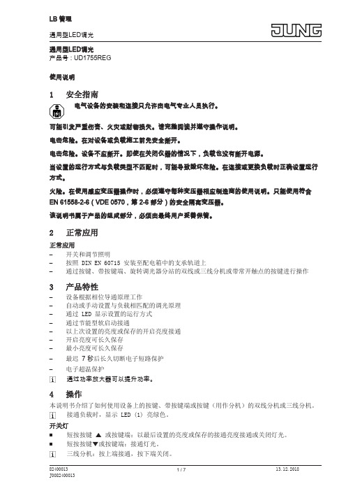
通用型LED调光产品号 : UD1755REG使用说明1安全指南电气设备的安装和连接只允许由电气专业人员执行。
可能引发严重伤害、火灾或财物损失。
请完整阅读并遵守操作说明。
电击危险。
在对设备或负载施工前先安全断开。
电击危险。
设备不应断开。
即使在关闭仪器的情况下,负载也没有断开电源。
当设置的运行方式与负载类型不匹配时,可能导致毁坏危险。
在连接或更换负载时正确设置运行方式。
火险。
在使用感应变压器操作时,必须遵守每种变压器相应制造商的使用说明。
只能使用符合EN 61558-2-6(VDE 0570,第 2-6 部分)的安全隔离变压器。
该说明书属于产品的组成部分,必须由最终用户妥善保管。
2正常应用正常应用–开关和调节照明–按照 DIN EN 60715 安装至配电箱中的支承轨道上–通过按键、带按键端、旋转调光器分站的双线或三线分机或带常开触点的按键进行操作3产品特性–设备根据相位导通原理工作–自动或手动设置与负载相匹配的调光原理–通过 LED 显示设置的运行方式–通过节能型软启动接通–以上次设置的亮度或保存的开启亮度接通–开启亮度可长久保存–最小亮度可长久保存–最迟 7 秒后长久切断电子短路保护–电子超温保护通过功率放大器可以提升功率。
4操作本说明书介绍了如何使用设备上的按键、带按键端或按键(用作分机)的双线分机或三线分机。
接通负载时,显示 LED (1) 亮绿色。
开关灯■短按按键 n 或按键端:以最后设置的亮度或保存的接通亮度接通或关闭灯光。
■短按按键o或按键端:接通灯光。
三线分机:按上端接通,按下端关闭。
设置亮度灯已开。
■长按按键 n 或按键上端。
灯光变亮至最大亮度。
■长按按键 o 或按键下端。
灯光变暗至最小亮度。
以最小亮度打开灯■长按按键 o 或按键下端。
将灯开到最小亮度。
■长按按键 n 或按键上端。
将灯开到最小亮度并且灯光变亮。
保存开启亮度发货时会将最大亮度设置为开启亮度。
■将灯调节至所需亮度。
■全方位长按按键 n 和 o 或按键端 4 秒。
欧司朗LED规格书
F4152AHigh Efficiency 40 mil ThinGaN ®LED (455nm)2007-09-131Features •High efficiency due to new ThinGaN ® concept •Lambertian Emission pattern•Ideal for LCD backlighting and coupling in light guides •Polarity: n-side up•Wavelength (typ.): 455 nm •Technology: ThinGaN ®•Grouping parameters: luminous intensity, wavelengthApplications •Outdoor displays •Optical indicators•Backlighting (LCD, switches, keys, displays, illuminated advertising, general lighting)•Marker lights (e.g. steps, exit ways, etc.)•Signal and symbol luminaireType Ordering Code DescriptionF4152AQ65110A704040 mil high efficiency ThinGaN ® chip, 450 - 465 nmElectrical values1)(T A = 25 °C)Parameter Symbol Value2)Unitmin.typ.max. Dominant wavelengthI F = 350 mA, pulsedλdom450465nm Reverse voltageI R = 10µAV R10VForward voltageI F = 350 mA, pulsed VF2.73.8VRadiant PowerI F = 350 mA, pulsedΙV32 a.u.1)Measurement limits describe actual settings and do not include measurement uncertainties. Each wafer and fragmentof a wafer is subject to final testing. The wafer or its pieces are individually attached on foils (rings). All el. values are referenced to the vendor's measurement system (correlation to customer product(s) is required). Measurement uncertainty +/-15% for brightness, +/- 1nm for wavelength and +/- 0.1V for voltage.2)Due to the special conditions of the manufacturing processes of LED, the typical data or calculated correlations oftechnical parameters can only reflect statistical figures. These do not necessarily correspond to the actual parameters of each single product, which could differ from the typical data and calculated correlations or the typical characteristic line. If requested, e.g. because of technical improvements, these typ. data will be changed without any further notice.2007-09-1322007-09-133Binning Maximum Ratings 1)Radiant Power 450 - 455 nm455 - 460 nm460 - 465 nm28.0 - 35.2 a.u.A1B1C135.2 - 41.2 a.u.A2B2C241.2 - 48.4 a.u.A3B3C348.4 - 56.8 a.u.A4B4C4> 56.8 a.u.A5B5C5ParameterSymbol Value Unit Maximum Operating temperature range T op -40...+100°C Maximum forward current (T A = 25°C)I F 700mA Minimum forward current (T A = 25°C)I F100mA Maximum surge Current (T A = 25°C)t p = 10 µs, D = 0.05I peak0.7A Maximum junction temperatureT j125°C1)Maximum ratings are strongly package dependent and may differ between different packages. The values given represent the chip in an OSRAM Opto Semiconductor’s Platinum Dragon® package.Mechanical values1)Parameter Symbol Value2)Unitmin.typ.max.Length of chip edge (x-direction)L x0.95 1.00 1.05mm Length of chip edge (y-direction)L y0.95 1.00 1.05mm Diameter of the wafer D50.8mmDie height H170190210µm Diameter of bondpad d130150170µm Additional informationMetallization frontside Gold partialMetallization backside AuDie bonding Epoxy bonding1)All chips are checked according to the following procedure and the OSRAM OS specification of the visual inspectionA63501-Q0013-N001-*-76G3:Unless otherwise described below, the quality level of the final visual inspection shall comply to an AQL 0,4 (according MIL-STD-105D, level II), if the customer performes an incoming visual inspection of a shipment. The quality inspection (final visual inspection) is performed by production. An additional visual inspection step as special release procedure by QM after the final visual inspection is not installed.2)Due to the special conditions of the manufacturing processes of LED, the typical data or calculated correlations oftechnical parameters can only reflect statistical figures. These do not necessarily correspond to the actual parameters of each single product, which could differ from the typical data and calculated correlations or the typical characteristic line. If requested, e.g. because of technical improvements, these typ. data will be changed without any further notice2007-09-1342007-09-135Chip OutlinesDimensions are specified as typicalvalues as follows: mm (inch).Published by OSRAM Opto Semiconductors GmbH Wernerwerkstrasse 2, D-93049 Regensburg © All Rights Reserved.Attention please!The information generally describes the type of component and shall not be considered as assured characteristics or detailed specification.Terms of delivery and rights to change design reserved. Due to technical requirements components may contain dangerous substances. For information on the types in question please contact our sales organization.Handling and Storage Conditions:Storage time for wafers in sealed condition shall not exceed 6 months (storage ambient conditions: Ta=15...30°C;relative humidity: < 60%).The hermetically sealed shipment lot shall be opened under temperature and moisture controlled cleanroom environment only. Customer has to follow the according rules for disposition of material that can be hazardous for humans and environment. Dice have to be handled ESD sensitive.PackingChips are placed on a blue foil with minimum size of 18 x 18 cm².For shipment the wafers of a shipment lot are arranged to stacks. The stack is put in a plastic ESD bag with a maximum of 14 wafers in one bag. A maximum of 4 bags is put in a packaging box. A maximum of 5 packaging boxes is put in a shipping carton which is sealed for storage and shipment.Please use the recycling operators known to you. We can also help you – get in touch with your nearest sales office. By agreement we will take packing material back, if it is sorted. You will have to bear the costs of transport. For packing material that is returned to us unsorted or which we are not obliged to accept, we shall have to invoice you for any costs incurred.Label and shipping documentsEach wafer is identified with a sticker, which is attached to each wafer. The label shows chip type, wafer number, quantity, binning and the minimum, average and maximum values of voltage, luminous intensity and wavelength. Each wafer shipment includes an additional document, which summarizes the content.Design objectives a) workabilityThe chip design was developed and released based on the the vendor’s standard assembly procedures and packaging. Bond strength properties are in accordance to MIL_STD-750D, method 2037. Whether the chip fits to the customer’s product(c) with its according die and wire bond procedures and packaging must be evaluated by the customer himself. If workability problems arise after this release a mutually conducted problem solving procedure has to be set up, if thechips are suspected of contributing to the problemsb) chip characteristicsThe chips are produced by the vendor with best effort, but on chip level a subset of the chip characteristics can be determined only. Performance of the chip in the customer’s product(s) can only be determined by the customer himself. Returns/ComplaintsTo return material because of technical or logistical reasons a RMA-number is necessary. Samples for analysis purposes can be send to OSRAM OS without credit.Shipping Conditions:If not otherwise arranged, the “General Conditions for the supply of products and services of the electrical and electronics industry” apply for any shipment. If these documents are not familiar to you, please request them at our nearest sales office.Components used in life-support devices or systems must be expressly authorized by us for such purpose! Critical components2), may only be used in life-support devices or systems3) with the express written approval of OSRAM OS.1) Typical (refered to as typ.) data are defined as long-term production mean values and are only given for information. This is not a specified value.2)A critical component is a component used in a life-support device or system whose failure can reasonably be expected to cause the failure of that life-support device or system, or to affect its safety or effectiveness of that device or system.3)Life support devices or systems are intended (a) to be implanted in the human body, or (b) to support and/or maintain and sustain human life. If they fail, it is reasonable to assume that the health of the user may be endangered.2007-09-136。
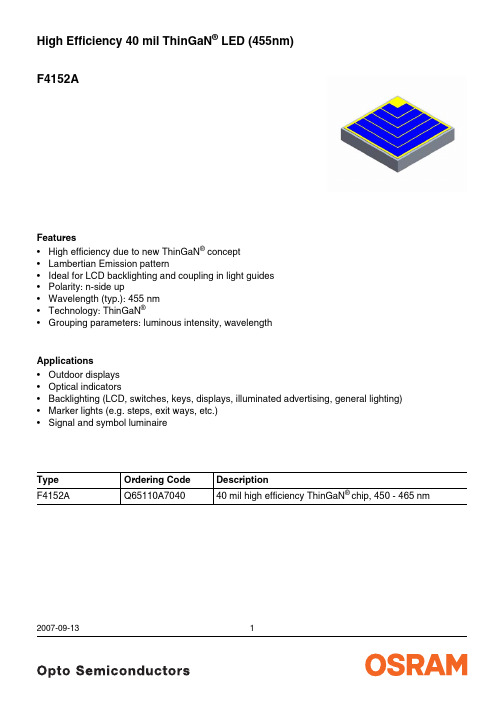
LED模组规格书

1020
>70
140
72×150°偏光25°85×145°
60
3030
72
DC48V
1230
>70
130
72×150°偏光25°85×145°
80
3030
112
DC48V
1640
>70
160
72×150°偏光25°85×145°
TS-MZ3XX 模组系列
72×150° 配光曲线
85×145° 配光曲线
3030
72
DC48V
1020
>70
140
72×150°偏光25°85×145°
TS-MZ373
50
3030
72
DC48V
1020
>70
140
72×150°偏光25°85×145°
60
3030
112
DC48V
1230
>70
130
72×150°偏光25°85×145°
TS-MZ374
50Leabharlann 303072DC48V
安装说明
模组尺寸(mm)
装箱数量(个)
外箱尺寸(mm)
净重(kg)
毛重(kg)
300×60×35
20
380×313×258
10.5
14
300×70×35
20
380×313×258
11.2
15
300×70×47
20
380×313×258
12
16
1、选择灯具的配光角度为72×150°时,灯具模组上有指示朝向的箭头,如下图红色方框内示例。灯具安装时,应确保模组上箭头所指的方向朝照射方向安装。2、选择灯具配光角度为85×145°时,则不限定安装方向。
荧光灯灯管参数表
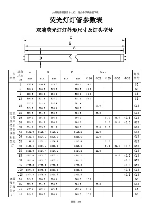
35
1449.0
1453.7
1456.1
1463.2
17.0
G5
39
849.0
853.7
856.1
863.2
17.0
G5
54
1149.0
1153.7
1156.1
1163.2
17.0
G5
80
1449.0
1453.7
1456.1
1463.2
17.0
G5
快速启动荧光灯
20
589.8
594.5
596.9
1204.1
1206.5
1213.6
31.0
G13
40
1199.4
1204.1
1206.5
1213.6
31.0
31.4
40.5
G13
58
1500.0
1504.7
1507.1
1514.2
28.0
G13
65
1500.0
1504.7
1507.1
1514.2
31.4
40.5
G13
80
1500.0
1504.7
118
138
255
高频预热阴极荧光灯启动特性
频率/KHZ
标称功率
标称管径/mm
试验电流
各阴极电阻
/W
额定值
最小值
最大值
20 ~ 26
14
16
160
40
30
50
21
24
28
35
24
350
12
8
15
39
LED平板灯规格书1
4U
4U
阳光照明
2U
4U
屏蔽室LED灯安装案例
阳光照明
屏蔽室LED灯选型
屏蔽室照明:
型号:BP60-60-D,安装尺寸:600X600X35mm;功率:30W,屏蔽室按照30m² , 每个屏蔽室安装6个,可超出500LM/m² 屏蔽室要求;可选用颜色:冷白、正白、 暖白。
设备轮廓照明:
阳光照明led灯技术参数序号参数60x6060x120射灯壁灯壁灯备注功率30w60w5w3w5w色温2500k7800k显色指数ra65ra光通量lm33006600660330660寿命寿命80000小时重量185kg37kg115kg072kg126kg阳光照明led灯技术参数序号参数60x6060x120射灯壁灯壁灯备注输入电压85265v5060hz功率因数pf095电源效率97输出电压dc
阳光照明
LED灯技术参数
序号 1 2 3 4 5 6 7 8 参数 功率 色温 显色指数 光通量lm 发光颜色 寿命 重量 价格 1.85Kg ? 3300 60X60 30W 60X120 60W 射灯 5W 2500K-7800K Ra ≧ 65 /Ra ≧ 80 6600 660 330 660 壁灯 3W 壁灯 5W 备注
正白、暖白、冷白
正白、暖白、冷白、红、黄、 可定 蓝、绿 制 1.15Kg ? 0.72Kg ? 1.26Kg ?
寿命≧80000小时 3.7Kg ?
阳光照明
LED灯技术参数
序号 1 参数 输入电压 60X60 60X120 射灯 壁灯 壁灯 备注 85-265V/50-60HZ
2
3 4 5 6
功率因数
电源效率 输出电压 功率 MTBF
P10技术规格书
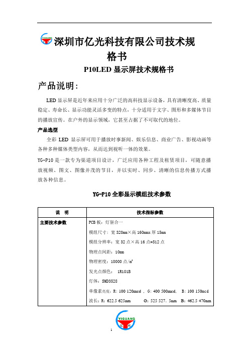
深圳市亿光科技有限公司技术规
格书
P10LED显示屏技术规格书
产品说明:
LED显示屏是近年来应用十分广泛的高科技显示设备,具有清晰度高、质量稳定、寿命长、显示功能灵活多变的特点,十分适用于文字、图形和多媒体节目的播放宣传。
在户外的显示领域,它甚至占据了不可取代的地位。
产品选型
全彩LED显示屏可用于播放时事新闻、娱乐信息、商业广告、影视动画等各种多种媒体类型内容,从而达到视听一体的效果。
YG-P10是一款专为渠道项目设计,广泛应用各种工程及租赁项目,可随意播放视频、图文、图像并茂的节目,并以实时、同步、清晰的信息传播方式播放各种信息。
YG-P10全彩显示模组技术参数。
国光亮光绿色LED设备数据手册说明书

DESCRIPTIONThe Green source color devices are made with Gallium Phosphide Green Light Emitting DiodeFEATURESLow power consumptionPopular T-1 diameter package General purpose leads Reliable and ruggedLong life - solid state reliability Available on tape and reel RoHS compliantAPPLICATIONSStatus indicator IlluminatorSignage applicationsDecorative and entertainment lightingCommercial and residential architectural lightingPACKAGE DIMENSIONSWP710A10GDT-1 (3mm) Solid State LampNotes:1. All dimensions are in millimeters (inches).2. Tolerance is ±0.25(0.01") unless otherwise noted.3. Lead spacing is measured where the leads emerge from the package.4. The specifications, characteristics and technical data described in the datasheet are subject to change without prior notice.Notes:1. θ1/2 is the angle from optical centerline where the luminous intensity is 1/2 of the optical peak value.2. Luminous intensity / luminous flux: +/-15%.3. Luminous intensity value is traceable to CIE127-2007 standards.ParameterSymbol Value Unit Power Dissipation P D 62.5 mW Reverse Voltage V R 5 V Junction Temperature T j 110 °C Operating Temperature T op -40 To +85 °C Storage Temperature T stg -40 To +85°C DC Forward Current I F 25 mA Peak Forward CurrentI FM [1]140 mA Electrostatic Discharge Threshold (HBM) -8000 V Thermal Resistance (Junction / Ambient) R th JA [2] 680 °C/W Thermal Resistance (Junction / Solder point) R th JS [2]460°C/WLead Solder Temperature [3] 260°C For 3 Seconds Lead Solder Temperature [4]260°C For 5 SecondsABSOLUTE MAXIMUM RATINGS at T A =25°CELECTRICAL / OPTICAL CHARACTERISTICS at T A =25°CParameterSymbol Emitting ColorValue Unit Typ. Max. Wavelength at Peak Emission I F = 10mA λpeak Green 565 - nm Dominant Wavelength I F = 10mA λdom [1] Green 568 - nm Spectral Bandwidth at 50% Φ REL MAX I F = 10mA ∆λ Green 30 - nm CapacitanceC Green 15 - pF Forward Voltage I F = 10mA V F [2] Green 2 2.4 V Reverse Current (V R = 5V) I R Green - 10 µA Temperature Coefficient of λpeak I F = 10mA, -10°C ≤ T ≤ 85°C TC λpeak Green 0.1 - nm/°C Temperature Coefficient of λdom I F = 10mA, -10°C ≤ T ≤ 85°C TC λdom Green 0.06 - nm/°C Temperature Coefficient of V F I F = 10mA, -10°C ≤ T ≤ 85°CTC VGreen-2-mV/°CNotes:1. The dominant wavelength (λd) above is the setup value of the sorting machine. (Tolerance λd : ±1nm. )2. Forward voltage: ±0.1V.3. Wavelength value is traceable to CIE127-2007 standards.4. Excess driving current and / or operating temperature higher than recommended conditions may result in severe light degradation or premature failure.Notes:1. 1/10 Duty Cycle, 0.1ms Pulse Width.2. R t h JA ,R t h JS Results from mounting on PC board FR4 (pad size ≥ 16 mm 2 per pad).3. 2mm below package base.4. 5mm below package base.5. Relative humidity levels maintained between 40% and 60% in production area are recommended to avoid the build-up of static electricity – Ref JEDEC/JESD625-A and JEDEC/J-STD-033.TECHNICAL DATAGREENRECOMMENDED WAVE SOLDERING PROFILENotes:1. Recommend pre-heat temperature of 105°C or less (as measured with a thermocoupleattached to the LED pins) prior to immersion in the solder wave with a maximum solder bath temperature of 260°C2. Peak wave soldering temperature between 245°C ~ 255°C for 3 sec (5 sec max).3. Do not apply stress to the epoxy resin while the temperature is above 85°C.4. Fixtures should not incur stress on the component when mounting and during soldering process.5. SAC 305 solder alloy is recommended.6. No more than one wave soldering pass.PACKING & LABEL SPECIFICATIONSPRECAUTIONSStorage conditions1. Avoid continued exposure to the condensing moisture environment and keep the product away from rapid transitions in ambient temperature.2. LEDs should be stored with temperature ≤ 30°C and relative humidity < 60%.3. Product in the original sealed package is recommended to be assembled within 72 hours of opening. Product in opened package for more than a week should be baked for 30 (+10/-0) hours at 85 ~ 100°C.2. When soldering wires to the LED, each wire joint should be separately insulated with heat-shrink tube to prevent short-circuit contact. Do not bundle both wires in one heat shrink tube to avoid pinching the LED leads. Pinching stress on the LED leads may damage the internal structures and cause failure.3. Use stand-offs (Fig.1) or spacers (Fig.2) to securely position the LED above the PCB.4. Maintain a minimum of 3mm clearance between the base of the LED lens and the first lead bend (Fig. 3 ,Fig. 4).5. During lead forming, use tools or jigs to hold the leads securely so that the bending force will not be transmitted to the LED lens and its internal structures. Do not perform lead forming once the component has been mounted onto the PCB. (Fig. 5 )LED Mounting Method1. The lead pitch of the LED must match the pitch of the mounting holes on the PCB during component placement.Lead-forming may be required to insure the lead pitch matches the hole pitch.Refer to the figure below for proper lead forming procedures.Note 1-3: Do not route PCB trace in the contact area between the leadframe and the PCB to prevent short-circuits." ○" Correct mounting method " x " Incorrect mounting methodLead Forming Procedures1. Do not bend the leads more than twice. (Fig. 6 )2. During soldering, component covers and holders should leaveclearance to avoid placing damaging stress on the LED during soldering.(Fig. 7)3. The tip of the soldering iron should never touch the lens epoxy.4. Through-hole LEDs are incompatible with reflow soldering.5. If the LED will undergo multiple soldering passes or face otherprocesses where the part may be subjected to intense heat,please check with Kingbright for compatibility.PRECAUTIONARY NOTES1. The information included in this document reflects representative usage scenarios and is intended for technical reference only.2. The part number, type, and specifications mentioned in this document are subject to future change and improvement without notice. Before production usage customer should refer tothe latest datasheet for the updated specifications.3. When using the products referenced in this document, please make sure the product is being operated within the environmental and electrical limits specified in the datasheet. Ifcustomer usage exceeds the specified limits, Kingbright will not be responsible for any subsequent issues.4. The information in this document applies to typical usage in consumer electronics applications. If customer's application has special reliability requirements or have life-threateningliabilities, such as automotive or medical usage, please consult with Kingbright representative for further assistance.5. The contents and information of this document may not be reproduced or re-transmitted without permission by Kingbright.6. All design applications should refer to Kingbright application notes available at https:///ApplicationNotes。
亿光led规格书(204-10asubw-s400-a5)

Label Form Specification
CPN: P/N:
EVERLIGHT
204-10ASUBW/S400-A5
QTY:
CAT:
LOT NO:
HUE: REF:
204-10ASUBW/S400-A5
CPN: Customer’s Production Number P/N : Production Number 204-10ASUBW/S400-A5:Production name QTY: Packing Quantity CAT: Ranks of Luminous and Forward Voltage HUE: Ranks of Dominant Wavelength REF: Reference LOT No: Lot Number MADE IN TAIWAN: Production Place
․Lead spacing is measured where the lead emerges from the package.
․Protruded resin under flange is 1.5mm Max LED.
Absolute Maximum Ratings (Ta=25℃)
Parameter
The reliability of products shall be satisfied with items listed below. Confidence level:97% LTPD:3%
NO
Item
1
Solder Heat
Temperature 2
Cycle
Test Conditions
Symbol
Rating
Units
LED照明产品资料整理
反光制作工艺 ABS 反光内表面镜面镀铝
2020/7/17
7210 节能强光防爆手电筒
光源
流明
总光通量
100lm (1*3W)
中心光强
2580cd
反光杯尺寸 27.7*30mm
反光制作工艺 ABS 反光内表面镀镜面镀铝
2020/7/17
7400 多功能强光防爆电筒
光源
Cree XR-E Q4
2020/7/17
7510 固态免维护强光电筒
光源
Cree XR-E P4
总光通量
130lm (1*3W)
中心光强
4300cd
反光杯尺寸 35*50mm
反光制作工艺 ABS 反光内表面镜面镀铝
2020/7/17
7610 战术灯
光源
流明
总光通量
60lm (1*1W)
中心光强
1690cd
2020/7/17
5120 便携式免维护强光防爆工作灯
光源
流明
总光通量
60lm (1*3W)
中心光强
1870cd
反光杯尺寸 47*39.7mm
反光制作工艺 PC241 反光内表面镜面镀铝
2020/7/17
5130 微型防爆头灯
光源
流明
总光通量
100lm (1*3W)
中心光强
2100cd
2020/7/17
7622 多功能强光巡检灯
光源
Cree XR-E Q4
总光通量
110lm (1*1W)
中心光强
3840cd
反光杯尺寸 26.3*21mm
反光制作工艺 ABS 反光内表面镜面镀铝
2020/7/17
UVLED 点光源说明书
UVLED点光源说明书编辑及出版说明本说明书由本公司编辑出版,说明书中包含有最新产品的说明和技术规格。
本说明书的内容及产品规格如有更改,恕不另行通知。
同时由于使用说明书所包含的材料所造成的任何损坏(包括后果),包括但不限于出版物的排版及其他错误。
上海润铸电子科技有限公司将不承担任何责任。
安全警告:警告如何避免可能的人身伤害,照射头放射出的紫外线对人体有害, 请勿照射人体尤其是眼睛,使用时请佩戴RUNLED 保护眼镜。
警告高温,使用及刚使用完设备后,照射头温度非常高,为避免受伤, 请勿触碰。
请勿用湿手拔电源插头,避免可能的电击。
重要安全说明使用设备时,为减少发生火灾,电击和人身伤害的可能性,请严格遵守下列基本安全指南1、请勿在水源附近,潮湿的地方使用本产品。
2、避免在雷雨期间使用本产品。
否则可能由于闪电而导致电击的危险。
3、请勿在煤气,天然气等可燃气体泄漏区域附近使用本产品。
请妥善保管本说明书。
简介1、包装箱内部品清单1、控制器2、照射头3、脚踏开关4、电源线5、使用说明书6、出厂合格证书注意:请注意清点各物品数量是否符合订单。
2、安装要求1、设备需要放置在一个平整、牢固而不易受到振动和拦击的表面上。
2、设备需要在室温(不超过40℃)下进行工作注意:请勿将设备安装在加热器、空调、流体、化学制品附近。
请勿将设备暴露在阳光直射、过热、潮湿或多尘的地方。
请勿将设备连接到与大功率设备共用同一电路的插座上。
请勿撞击或触摸镜头。
3、控制面板概述①液晶显示屏(LCD)②方向键使用此键可以进行功能和设定操作。
同时在4通道设备中,可作为4个照射头(CH1/CH2/CH3/CH4)开关控制按键。
③取消键(ESC) 停止操作或从功能菜单中退出。
④保存键(ENT) 使用此键可以将设置存储在设备中。
⑤设置键(SET) 使用此键可以进入设定模式。
⑥运行/停止键(RUN) 程序运行或停止。
4、后面板概述① RS232接口。
亿光shwo系列LED规格书

IntroductionThe Shwo series is a surface-mount high-power device featuring high brightness combined with a compact size that is suitable for all kinds of lighting applications such as general illumination, flash, spot, signal, industrial and commercial lighting. The thermal pad of this device is electrically isolated providing convenience inthermal andelectrical design. TheShwo series is one of the most promising devices in Everlight’s high power product offering and is ready to face the challenges of today’s Solid-State Lighting requirements.Shwo1W Series爍“Shwo [Shuo] is the English translation for the Chinese word meaning Twinkle and is often used as a description of stars or other bright, celestial objects as seen from Earth. This word is a relevant description for this bright, compact Everlight LED package.”Table of ContentsProduct Nomenclature (3)Absolute Maximum Ratings (4)JEDEC Moisture Sensitivity (4)Luminous Flux Characteristics for the Shwo series (5)PN of the Shuen High Luminous Series: White LEDs (7)PN of the Shwo series: Color LEDs (9)White Bin Structure (11)Forward Voltage Bins (16)Color Bins (17)Optical Characteristics (18)Mechanical Dimension (19)Pad Configuration (20)Reflow Soldering Characteristics (21)Wavelength Characteristics (22)Typical Light Output Characteristic vs. Thermal Pad Temperature (24)Typical Electrical Characteristics (25)Typical Relative Luminous Flux vs. Forward Current (26)Typical Wavelength & CCT Shift Characteristics (28)vs. Forward Current (28)Current Derating Curves (29)Typical Radiation Patterns (31)Emitter Tape Packaging (33)Emitter Reel Packaging (34)Product Labeling (34)Storage Conditions (35)Revision History (36)Product Nomenclature The product name is designated as below:ELSW – ABCDE – FGHIJ – V1234 Designation:AB = min. luminous flux (lm) or radiation power (mW) performanceC = radiation pattern [1]D = color [2]E = power consumption [3]F = reserved for future product offeringsG = Internal codeH = packaging type [4]IJ = internal codeV = forward voltage bin1234 = color bin or CCT binNotes1. Table of radiation patterns1 Lambertian2. Table of color offerings:R Red 620~630nmO Orange 610~620nmY Amber 585~595nmG Green 520~535nmB Blue 460~470nmC Cool-White 4745~7050KN Neutral-White 3710~4745KM Warm-White 2580~3710K3. Table of power consumptions:1 1W4. Table of packaging types:P TapeB TubeAbsolute Maximum RatingsSymbol Ratings Unit Max. DC Forward Current (mA) I F400[1]mAMax. Peak Pulse Current (mA) I Pulse1000[2]mA Max. ESD Resistance V B8000 VReverse Voltage V R Note 3 VThermal Resistance R th10 ~ 12[4]°C/W Max. Junction Temperature T J125[5]°COperating Temperature T Opr-40 ~ +100[6]°CStorage Temperature T Stg-40 ~ +100 °C Max. Soldering Temperature T Sol260 °CMax. Allowable Reflow Cycles n/a 2 cycles Notes:1. Maximum forward current for 1W is 400mA (T Thermal Pad=25°C),2. Duty cycle = 1/10@1Khz3. The Shuen series LEDs are not designed for reverse bias used.4. Thermal Resistance is 10°C/W for Blue, Green, Cool-White, Neutral-White,and Warm-White LEDs and 12°C/W forRed, Amber, and Orange LEDs.5. Maximum junction temperature of Cool-White, Neutral-White, Warm-White, Blue, Green, Red, Amber, and OrangeLEDs is 125°C.6. Maximum Operating Temperature (Thermal Pad) of Cool-White, Neutral-White, Warm-White, Blue, Green, Red,Amber, and Orange LEDs is 100°C.JEDEC Moisture SensitivitySoak RequirementsStandardTimeConditions(hours)1 Unlimited ≦30°C / 85% RH 168 (+5/-0) 85°C / 85% RHLuminous Flux Characteristics for the Shwo seriesNotes:1. Luminous flux measurement tolerance: ±10%.2. The data of luminous flux measured at thermal pad=25℃3. Typical luminous flux or light output performance is operated within the condition guided by this datasheet.PN of the Shwo series: White LEDsThe table below is a list of part numbers for the Everlight Shwo 1W series White LED. All parts listed match ANSI binning standards. Bin offerings of 2700K to 6500K are listed and currently available. CRI is also listedwith min 70 to 80. Typical view angle is 120°. These clearly listed binning options allow for proper design and implementation into lighting applications. The Order Codes below are currently available White Shwo LEDs. For Example: If you order product using P/N ELSW-F81C1-0LPGS-C5700, you will get White, Shwo seriesLEDs at 350mA are listed belowNote:1. CRI measurement tolerance: ±2.Color RadiationPatternCRICCT Forward Voltage (V) MinimumLuminousFlux (lm)CoolWhite Lambertian 70 57K-1 ~ 57K-2 ~ 57K-3 ~ 57K-4 2.95~3.25(V1)3.25~3.55(V2) 3.55~3.85(V3)80PN of the Shuen High Luminous Series: White LEDsThe table below is a list of part numbers for the Everlight Shuen 1W high luminous series White LED. All parts listed match ANSI binning standards. Bin offerings of 2700K to 6500K are listed and currently available. CRI is also listed with min 70 to 80. Typical view angle is 110°. These clearly listed binning options allow for proper design and implementation into lighting applications. The Order Codes below are currently available White Shuen LEDs. For Example: If you order product using P/N ELSW-J11C1-0CPGS-C5700, you will get White , Shuen series LEDs at 350mA are listed below.Color Variant RadiationPattern CRICCT ForwardVoltage(V)Minimum Luminous Flux (lm)CoolWhiteLambertian 7057K-1 ~ 57K-2 ~ 57K-3 ~ 57K-4 2.95~3.25(V1)3.25~3.55(V2) 3.55~3.85(V3)1001. CRI measurement tolerance: ±2.9Copyright © 2011, Everlight All Rights Reserved. Release Date : 03282011. Issue No: DHE-0001156PN of the Shwo series: Color LEDsThe table below is a list of the binning options for the Everlight Shwo 1W series Color LED. Standard Everlight color bins are listed according to wavelength and represent the standard primary colors of the spectrum. Typical view angle is 120°. These clearly listed binning options allow for proper design and implementation into lighting applications. The Order Codes below are currently available Color Shwo LEDs.For Example: If you order product using P/N ELSW-F51R1-0LPNM-AR5R6, you will be specifying: Color, Shwo series LEDs at 350mA are listed below.Color Variant RadiationPattern Dominant Wavelength(nm)Forward Voltage (V) Minimum Luminous Flux (lm) RedLambertian620~625(R5)625~630(R6)1.75~2.05(U1) 2.05~2.35(U2) 2.35~2.65(U3)5210Product BinningLuminous Flux BinsGroup Bin Minimum Photometric Flux (lm)Maximum Photometric Flux (lm)1 4 5 1 100 1102 5 6 2 110 1203 6 8 3 120 1304 8 10 4 130 1405 10 13 5 140 1506 13 17 6 150 160 7 17 20 7 160 1808 20 23 8 180 200 E9 23 27 J9 200 225 1 27 33 1 225 250 2 33 39 2 250 275 3 39 45 3 275 300 4 45 52 4 300 325 5 52 60 5 325 350 6 60 70 6 350 375 7 70 80 7 375 400 8 80 90 8 400 425 F 9 90100K9 425 450 1 450 4752 475 500N3500525Note: Currently available brightness bins for White LEDs are highlighted and bolded.Radiometric Power BinsGroup Bin Minimum Radiometric Power(mW)Maximum Radiometric Power(mW)1 0 25 1 350 4252 25 50 2 425 5003 50 75 3 500 6004 75 100 4 600 700 5 100 125 5 700 8006 125 175 6 800 9007 175 225 7 900 10008 225 275 8 1000 1300 Q 9275350R913001600White Bin StructureNotes:1. The CCT range of Cool-White varies from 4745K to 7050K.2. The CCT range of Neutral-White varies from 3710K to 4745K.3. The CCT range of Warm-White varies from 2580K to 3710K4. Color coordinates measurement allowance : ±0.015.Color bins are defined at I F =350mA operation.Cool-White Bin StructureChromaticity specification defined by ANSICool-White Bin Coordinates5000KBinCIE X CIE Y 0.346 0.369 0.338 0.362 0.345 0.3560.337 0.3490.353 0.362 0.345 0.356 50K-10.355 0.37650K-20.346 0.369Reference Range: 4745~5000K Reference Range: 5000~5310K Bin CIE X CIE Y0.345 0.356 0.337 0.349 0.344 0.3430.337 0.3370.352 0.349 0.344 0.343 50K-40.353 0.36250K-30.345 0.356Reference Range: 4745~5000KReference Range: 5000~5310K 5700KBinCIE X CIE Y 0.329 0.354 0.321 0.346 0.329 0.3420.321 0.3350.337 0.349 0.329 0.342 57K-10.338 0.36257K-20.329 0.354Reference Range: 5310~5700KReference Range: 5700~6020KBin CIE X CIE Y0.329 0.342 0.321 0.335 0.329 0.3310.322 0.3240.337 0.337 0.329 0.331 57K-40.337 0.34957K-30.329 0.342Reference Range: 5310~5700K Reference Range: 5700~6020K6500KBinCIE X CIE Y 0.312 0.339 0.303 0.330 0.313 0.3290.305 0.3210.321 0.337 0.313 0.329 65K-10.321 0.34865K-20.312 0.339Reference Range: 6020~6500KReference Range: 6500~7050KBin CIE X CIE Y0.313 0.329 0.305 0.321 0.314 0.3190.307 0.3110.322 0.326 0.314 0.319 65K-40.321 0.33765K-30.313 0.329Reference Range: 6020~6500K Reference Range: 6500~7050KNeutral-White Bin StructureNeutral-White Bin Coordinates4000KCIE X CIE Y BinCIE X CIE Y 0.387 0.396 0.374 0.387 0.383 0.3800.370 0.3730.395 0.388 0.383 0.380 40K-10.401 0.40440K-20.387 0.396Reference Range: 3710~4000KReference Range: 4000~4260KCIE X CIE YBin CIE X CIE Y0.383 0.380 0.370 0.373 0.378 0.3650.367 0.3580.390 0.372 0.378 0.365 40K-40.395 0.38840K-30.383 0.380Reference Range: 3710~4000K Reference Range: 4000~4260K 4500KCIE X CIE Y BinCIE X CIE Y 0.3640.381 0.355 0.374 0.362 0.366 0.353 0.360 0.370 0.373 0.362 0.366 45K-10.3740.38745K-2 0.3640.381Reference Range: 4260~4500KReference Range: 4500~4745KCIE X CIE YBin CIE X CIE Y0.3620.366 0.353 0.360 0.359 0.352 0.351 0.347 0.367 0.358 0.359 0.352 45K-40.3700.37345K-3 0.3620.366Reference Range: 4260~4500KReference Range: 4500~4745KWarm-White Bin StructureWarm-White Bin Coordinates2700KCIE X CIE Y BinCIE X CIE Y 0.469 0.429 0.456 0.426 0.459 0.4100.447 0.4080.470 0.413 0.459 0.410 27K-10.481 0.43227K-20.469 0.429Reference Range: 2580~2700KReference Range: 2700~2870KCIE X CIE YBin CIE X CIE Y0.459 0.410 0.447 0.408 0.448 0.3920.437 0.3890.459 0.394 0.448 0.392 27K-40.470 0.41327K-30.459 0.410Reference Range: 2580~2700K Reference Range: 2700~2870K 3000KCIE X CIE Y Bin CIE X CIE Y 0.443 0.421 0.430 0.417 0.435 0.4030.422 0.3990.447 0.408 0.435 0.403 30K-10.456 0.42630K-20.443 0.421Reference Range: 2870~3000KReference Range: 3000~3220KCIE X CIE YBin CIE X CIE Y0.435 0.403 0.422 0.399 0.426 0.3850.415 0.3810.437 0.389 0.426 0.385 30K-40.447 0.40830K-30.435 0.403Reference Range: 2870~3000K Reference Range: 3000~3220K3500KBinCIE X CIE Y 0.415 0.409 0.400 0.402 0.408 0.3920.394 0.3850.422 0.399 0.408 0.392 35K-10.430 0.41735K-20.415 0.409Reference Range: 3220~3500KReference Range: 3500~3710KBin CIE X CIE Y0.408 0.392 0.394 0.385 0.402 0.3750.389 0.3690.415 0.381 0.402 0.375 35K-40.422 0.39935K-30.408 0.392Reference Range: 3220~3500K Reference Range: 3500~3710K Note: Currently available typical CCT ranges are 3000K, 5700K, and 6500K CCT.Forward Voltage BinsBinsA U1+U2+U3B U2+U3+U4C V1+V2+V3D V2+V3+V4Maximum ForwardVoltage (V)U1 1.75 2.05U2 2.05 2.35U3 2.35 2.65U4 2.65 2.95V1 2.95 3.25V2 3.25 3.55V3 3.55 3.85V4 3.85 4.15Notes:1. Forward voltage measurement tolerance: ±0.1V.2. Forward voltage bins are defined at I F=350mA operation.3. Currently available Forward Voltage bins for White LEDs are highlighted and bolded.4. Other Forward Voltage bins for White LEDs available upon request. Please contact your local Everlight sales office.Notes:1. Dominant wavelength measurement tolerance: ±0.5nm.2. Dominant wavelength bins are defined at I F=350mA operation.Optical CharacteristicsNotes:1. The test tolerance of Everlight is ±0.5nm for dominant wavelength, ±5% for CCT.2. Viewing angle is the width of half the light output intensity in all directions of 180°.3. All Cool-White, Neutral-White, Warm-White, and dominant wavelength below 550nm LEDs are made with Indium GalliumNitride (InGaN).4. All LEDs with dominant wavelength exceeding 550nm are made with Aluminum Indium Gallium Phosphide (AlInGaP).Mechanical DimensionNotes:1. Dimensions are in millimeters.2. Tolerances unless mentioned are ± 0.1mm.3. Do not handle the device by the lens. Incorrect force applied to the lens may lead to the failure of devices.4. The thermal pad is electrically isolated from the Anode and Cathode contact pads.Pad ConfigurationPAD FUNCTION1 ANODE2 CATHODEP THERMAL PADReflow Soldering CharacteristicsFor Reflow Processa. ELSW series are suitable for SMT processes.b. Curing of glue in oven must be according to standard operation flow processes.c. Reflow soldering should not be done more than twice.d. In soldering process, stress on the LEDs during heating should be avoided.e. After soldering, do not bend the circuit board.Wavelength CharacteristicsFor Red, Amber, Yellow, Green, Blue@ Thermal Pad Temperature = 25℃For Cool-White, @ Thermal Pad Temperature = 25℃For Neutral-White, @ Thermal Pad Temperature = 25℃For Warm-White, @ Thermal Pad Temperature = 25℃Typical Light Output Characteristic vs. Thermal Pad TemperatureCool-White, Neutral-White, Warm-White, Green, Bluefor 350mA Drive CurrentRed, Orange, Amber for 350mA Drive CurrentTypical Electrical CharacteristicsFor Cool-White, Neutral-White, Warm-White, Green, Blue @ Thermal Pad Temperature = 25℃For Red, Orange, Amber,@ Thermal Pad Temperature = 25℃Typical Relative Luminous Flux vs. Forward Current For Cool-White, Neutral-White, Warm-White@ Thermal Pad Temperature = 25℃For Green, Blue, @ Thermal Pad Temperature = 25℃For Red, Orange, Amber,@ Thermal Pad Temperature = 25℃Typical Wavelength & CCT Shift Characteristicsvs. Forward CurrentFor Cool-White @ Thermal Pad Temperature = 25℃For Neutral-White @ Thermal Pad Temperature = 25℃For Warm-White @ Thermal Pad Temperature = 25℃For Blue @ Thermal Pad Temperature = 25℃For Blue @ Thermal Pad Temperature = 25℃For Green @ Thermal Pad Temperature = 25℃For Green @ Thermal Pad Temperature = 25℃For Red @ Thermal Pad Temperature = 25℃Current Derating CurvesCurrent Derating Curve for 350mA Drive Current Cool-White, Neutral-White, Warm-White, Green, BlueCurrent Derating Curve for 350mA Drive CurrentRed, Amber, YellowTypical Radiation PatternsShwo series:Typical Diagram Characteristics of Radiationfor Cool-White, Neutral-White,Warm-White Lambertian0.00.20.40.60.81.0Viewing angle (degree)R e l a t i v e I n t e n s i t y (a .u .)-900-700-50-30-10908060704050302010Shwo High Luminous Series Typical Diagram Characteristics of RadiationforCool-White, Neutral-White, Warm-White Lambertian0.00.20.40.60.81.0Viewing angle (degree)R e l a t i v e I n t e n s i t y (a .u .)-900-700-50-30-10908060704050302010Notes:1. 2θ1/2 is the off axis angle from lamp centerline where the luminous intensity is 1/2 of the peak value.2. View angle tolerance is ± 5∘.Typical Difference of CIE X of Cool-White vs. AngleTypical Difference of CIE Y of Cool-White vs. AngleCarrier Tape Dimensions: Loaded quantity 400 PCS per reelFeed DirectionReel Dimensions1. Dimensionsare inmillimeters.2. Tolerancesunlessmentionedare±0.1mm.Product LabelingLabel ExplanationCPN: Customer Specification (when required)P/N : Everlight Production NumberQTY: Packing QuantityCAT: Luminous Flux (Brightness) BinHUE: Color BinREF: Forward Voltage BinLOT No: Lot NumberMADE IN TAIWAN: Production PlaceStorage ConditionsBefore the package is opened. The LEDs should be stored at 30°C or less and 85%RH or less after being shipped from Everlight and the storage life limits are 1 year. If the LEDs are stored for 1 year or more, they can be stored for 3 years in a sealed container with a nitrogen atmosphere and moisture absorbent material.After opening the package: The LED's floor life is 1 year under 30℃or less and 60%RH or less.The LED should be soldered with 168hrs (7days) after opening the package. If unused LEDs remain, it should be stored in moisture proof packages.If the moisture absorbent material (silica gel) has faded away or the LEDs have exceeded the storage time, baking treatment should be performed using the following conditions. Baking treatment: 60±5℃for 24 hours.Revision HistoryCurrent version: 2011/04/28Device No: DHE-0001156Version. 6.0Date of change6 Change the PN brightness level. 2010/06/1415 Change the viewing angle. 2010/06/1416 In the mechanical dimension, the polarity is changed. 2010/06/1417 In the pad configuration, the polarity is changed. 2010/06/143 Change the Product Nomenclature. 2010/08/264 Change the Absolute Ratings 2010.08.266-7 Change the PN brightness level. 2010/08/265 Change the PN brightness level. 2011/01/127、8、31、35 Added new PN, radiation patterns and storage conditions.2011/04/28。
亿光组装发光二极管LEDA214B-SUR-S530-A3规格书
EVERLIGHT ELECTRONICS CO.,LTD.Technical Data Sheet3.0mm Round Type LED LampsA214B/SUR/S530-A3█ Features :●Low power consumption●High efficiency and low cost●Good control and free combinationson the colors of LED lamps ●Good lock and easy to assembly ●Stackable and easy to assembly ●Stackable vertically and easy to assembly ●Versatile mounting on P.C board or panel ●Stackable horizontally and easy to assembly ●Pb free█ Descriptions :●ARRAY=Plastic Holder+Combinations of Lamps●The array will easily mount the applicable lamps on any panel up to█ Applications :●ed as indicators of indicating the Degree, Functions, Positions etc, in electronic instruments.ChipMaterial Emitted Color 264-10SURD/S530-A3AlGaInPHyper RedEVERLIGHT ELECTRONICS CO.,LTD.http : // REV.:2Page: 1 of 6Device Number :CDAE-021-048Prepared date:2004/7/17Prepared by:Guanxiu YuanBG0308053,R0302557Lens ColorRed DiffusedPART NO.EVERLIGHT ELECTRONICS CO.,LTD. Technical Data SheetNote: *1:I FP Conditions --Pulse Width ≦ 1msec and Duty ≦ 1/10.*2:Soldering time ≦ 5 seconds.EVERLIGHT ELECTRONICS CO.,LTD.http : // REV.:2Page: 2 0f 6 Device Number :CDAE-021-048Prepared date:2004/7/17 Prepared by: Guanxiu YuanEVERLIGHT ELECTRONICS CO.,LTD.Technical Data Sheet3.0mm Round Type LED LampsA214B/SUR/S530-A3Electro-Optical Characteristics (Ta=25℃)Min.Typ.Max.Unit I F =20mA / 2.0 2.4V V R =5V //10μA I F =20mA 63120/mcd I F =20mA /60/deg I F =20mA /632/nm I F =20mA /624/nm I F =20mA/20/nmEVERLIGHT ELECTRONICS CO.,LTD. http : // REV.:2Page:3 of 6Device Number :CDAE-021-048Prepared date:Prepared by:Guanxiu Yuan2004/7/17λp λd △λV F I R Iv 2θ1/2Dominant Wavelength Spectrum RadiationBandwidthParameter Condition Forward Voltage Reverse Current Luminous Intensity Viewing Angle Peak Wavelength SymbolDevice Number :CDAE-021-048Prepared date: Prepared by: Guanxiu Yuan2004/7/17EVERLIGHT ELECTRONICS CO.,LTD.Technical Data Sheet3.0mm Round Type LED LampsA214B/SUR/S530-A3█ Reliability test items and conditions:EVERLIGHT ELECTRONICS CO.,LTD.http : // REV.:2Page:5 of 6 Device Number :CDAE-021-048Prepared date: Prepared by: Guanxiu Yuan2004/7/17EVERLIGHT ELECTRONICS CO.,LTD.Technical Data Sheet3.0mm Round Type LED LampsA214B/SUR/S530-A3EVERLIGHT ELECTRONICS CO.,LTD.http : // REV.:2Page:6 0f 6 Device Number :CDAE-021-048Prepared date:2004/7/17Prepared by: Guanxiu Yuan。
