VSP 618 产品规格书
uP6182-DS-F0001
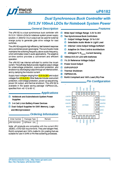
EN0 SKIPSEL GND VIN LDO5 VCLK
13 14 15 16 17 18
VREF VO1
VIN = 5.5~26V
VREG5
5V/100mA
15V/10mA
uPI Semiconductor Corp.,
2
Rev. F00, File Name: uP6182-DS-F0001
Wide Input Voltage Range: 5.5V to 26V Two Synchronous Buck Controllers
Output Voltage Range: 2V to 5.5V Selectable Audio Mode in Light Load Internal 1.6ms Output Voltage Softstart Adaptive On Time Control Architecture 4500ppm/OC RDS(ON) Current Sensing 100mA 5V/3.3V LDO with Switches 1% 2V Reference Voltage Output Power Good Output OVP/UVP/OCP Thermal Shutdown VQFN4x4-24L RoHS Compliant and 100% Lead (Pb)-Free
channel.
2
VFB1
Synchronous Buck Converter 1 Feedback Input. This pin is the inverting input to the error amplifier. A resistor divider from output to GND is used to set regulator voltage.
IEC 61850通信标准说明书
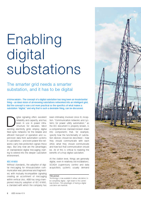
been intimately involved since its incep-tion. “Communication networks and sys-tems for power utility automation,” as the IEC document is properly known, is a comprehensive standard broken down into components that, for example, specify how the functionality of substa-tion devices should be described – how they should communicate with each o ther, what they should communicate and how fast that communication should be. All of this is critical to realizing the benefits of a truly digital substation.At the station level, things are generally digital, even in relatively old installations. SC ADA (supervisory control and data a cquisition) systems usually demand Digital signaling offers excellent reliability and capacity, and has been in use in power infra-structure for decades. Most existing electricity grids employ digital f iber-optic networks for the reliable and efficient transport of operation and su-pervision data from automation systems in substations – and even power line net-works carry tele-protection signals these days. But only now are the advantages of standardized digital messaging start-ing to extend into the deeper substation environment.IEC 61850Without standards, the adoption of digi-tal messaging for intrasubstation com-munication was piecemeal and fragment-ed, with mutually incompatible signaling creating an assortment of messaging within vertical silos. ABB has long cham-pioned industry adoption of IEC 61850, a standard with which the company has STEFAN MEIER – The concept of a digital substation has long been an insubstantial thing – an ideal vision of all-knowing substations networked into an intelligent grid. But the concept is now a lot more practical so the specifics of what makes a substation “digital,” and why that is such a desirable thing, can be discussed.The smarter grid needs a smarter substation, and it has to be digital Enabling digital substations Title picture Technology is now available to allow substations to be completely digital – right down to the currenttransformers. The advantages of having a digital substation are manifold.FOCS Robustness and reliability requirements apply to new technologies such as ABB’s fiber-optic current sensor (FOCS) too. A FOCS [1] can directly monitor current running through a high-voltage line with-out having to involve a current trans-former (CT) to step down the current to a measurable value. Eliminating the C T also eliminates the risk of open C T cir-cuits, in which life-threatening voltages can occur, and so increases safety.A FOCS exploits the phase shift in polar-ized light introduced by an electromag-netic field (the Faraday effect). The shiftis in direct proportion to the current flow-ing in the high-voltage line, around whichthe fiber carrying the light is wrapped.The measurement is digitized right atthe source and transmitted as a digitalsignal, via the process bus, to the pro-tection and control IEDs, as well as therevenue meters.Such an optical C T takes up a lot lessspace than its analog equivalent. It caneven be integrated into a disconnectingcircuit breaker (as ABB did in 2013) tocombine the functions of circuit breaker,current transformer and disconnector inone device – halving the size of a newsubstation.The FOCS is one of a range of noncon-ventional instrument transformers (NCITs)that can make things entirely digital.NCITs have to be every bit as reliable asthe equipment being replaced – and theydigital information and ABB has been selling fiber-optic “backbones” for more than two decades.Between the station level and the bays, fibers can carry digital data – conforming to IEC 61850 – but to become a true digital substation the standard has to e xtend even further.Deep digitalThe world beyond the bays is still pre-dominately analog. The conventional pri-mary equipment, like current and voltage transformers, is connected back to intel-ligent electronic devices (IEDs) using par-allel copper wires carrying analog voltage signals ➔1a. The IEDs receiving that data perform first-level analysis and often pro-vide the gateway into a digital world.But there is little advantage in keeping the data in analog form for so long and to properly earn the title of “digital substa-tion” the transition to digital must takeplace as soon as the data is gathered ➔1b.Through permanent system supervision, digital equipment reduces the need for manual intervention and the adoption of the all-digital process bus allows sensitive equipment to be relocated into the bays. The digital equipment that has to bel ocated out in the yard must be easy to fit, and every bit as robust and reliable as the analog equipment it is replacing or inter-facing to ➔2.Digital signaling offers excellent reliability and capacity, and has been in use in power infrastruc-ture for decades.1a Today 1b Tomorrow670 series 670 series REB500REB500650 series 650 seriescurrent transformer, arcing may occur as dangerously high voltages build and a copper line can suddenly carry high volt-age, putting workers and equipment at risk. Less copper brings greater safety.The digital substation dispenses with cop-per by using the digital process bus, which might use fiber optics or a wireless net-work, such as ABB’s Tropos technology.Just the removal of copper can, in some circumstances, justify the switch to digital. Going digital can cut the quantity of cop-per in a substation by 80 percent – a sub-stantial cost saving and, more importantly, a significant safety enhancement.The process bus also adds flexibility: Digital devices can speak directly to each other ➔3. For this, IEC 61850 defines the GOOSE (generic object-orientatedsubstation events)protocol for fasttransmission of bi-nary data. Part 9-2of the standard de-scribes the trans-mission of sampledvalues over Ether-net. These principlesensure the timelydelivery of high-pri-ority data via other-wise unpredictableEthernet links. ABB’s ASF range of E thernet switches fully supports this crit-ical aspect of substation messaging.are: Over the past decade ABB has sup-plied more than 300 NC ITs (combined current and voltage sensors fitted into gas-insulated switchgear) for use in Queensland, Australia, and the utility has yet to see a single failure in the primarysensor. Extensive use of NCITs makes a substation simpler, cheaper, smaller and more efficient.Not everything can be digital – analog data will continue to arrive from conven-tional current and voltage transformers, for example. But there is no reason for wholesale replacement when a stand-alone merging unit can perform the tran-sition to digital right beside the existinginstrument transformer. Fiber optics can then replace the copper cables connect-ing the primary equipment to the protec-tion and control IEDs.Process bus As a conductor, every bit of copper in a substation is a potential risk. For exam-ple, where current is incorrectly discon-nected, such as with an open secondary A FOCS can direct-ly monitor current running through a high-voltage line without having to involve a current transformer to stepdown the current to a measurable value.2 New equipment destined for use out in the yard is exposed to the elements so has to be very robust.ABB has long championed industry adoption of IEC 61850, a standard with which the company has been intimately involved since its inception.Installations ABB has been heavily involved in IEC 61850 since its inception. The stan-dard is essential to ensure that utilities can mix and match equipment from dif-ferent suppliers, but, through compli-ance testing, it also provides a bench-mark against which manufacturers can be measured.ABB deployed the first commercial IEC 61850-9-2 installation in 2011 at the Loganlea substation, for Powerlink Queens-land. The use of ABB’s IEC 61850-9-2- compliant merging units and IEDs, not to mention NCITs, makes the deployment a landmark in the evolution of substation design.That project was part of an upgrade of an existing station, an upgrade that saw it move into an IEC 61850 future, adopting digital standards for effective future-proof-ing. ABB created a retrofit solution based on specifications from Powerlink that can be applied to another five Powerlink substa-tions when they are ready for refitting.Two of those stations, Millmerran and Bulli Creek, were already upgraded in 2013 and 2014, respectively. The refurbished sub-stations have a MicroSCADA Pro SYS600 system and RTU560 gateway that manage Relion 670 protection and control IEDs, with REB500 busbar protection. These all communicate over IEC 61850-9-2 to the merging units and over IEC 61850 to the station-level devices. A fully digital substation is smaller, more reliable, has a reduced life-cycle cost and is simpler to maintain and extend than an analog one. It offers increased safety and is more efficient than its ana-log equivalent.Not every substation needs to be cata-pulted into a wholesale digital world – it depends on the substation size and type, and whether it is a new station or a retrofit of the secondary system. Different ap-proaches and solutions are required. ABB’s extensive IEC 61850 experience and portfolio of NCITs, merging units, pro-tection and control IEDs as well as station automation solutions eases utilities into the digital world. Flexible solutions allow utilities to set their own pace on their waytoward the digital substation.3 IEC 61850 makes the fully digital substation a reality.Stefan MeierABB Power Systems Baden, Switzerland *******************.com An optical CT takes up a lot less space than its analog equivalent and can even be integrated into a disconnecting circuit breaker to combine the func-tions of circuit breaker, current transformer and disconnector in one device – halv-ing the size of a new substation.Reference [1] S. Light measures current – A fiber-optic current sensor integrated into a high-voltage circuit breaker. Available: /global/scot/scot271.nsf/veritydisplay/0d948cedb40451cec1257ca900532dd0/$file/12-17%201m411_EN_72dpi.pdf。
杰尼斯科技产品选购指南说明书
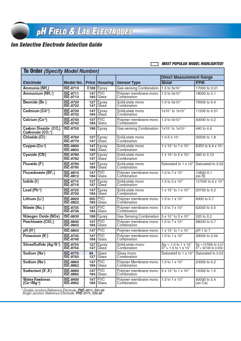
MOST POPULAR MODEL HIGHLIGHTED!Single Junction Reference Electrode, PHE-3111,£35.50Comes with complete operator’s manual.Ordering Examples:ISE-8711,ammonium electrode,£147.ISE-8756,silver/sulfide electrode,£147.C-22PHI-359,£845,bench toppH meter shown smallerthan actual size,see page B-33.C-23CANADA www.omega.ca Laval(Quebec)1-800-TC-OMEGA UNITED KINGDOM Manchester,England0800-488-488GERMANY www.omega.deDeckenpfronn,Germany************FRANCE www.omega.fr 088-466-342BENELUX www.omega.nl 0800-099-33-44UNITED STATES 1-800-TC-OMEGA Stamford,CT.CZECH REPUBLIC www.omegaeng.cz Karviná,Czech Republic596-311-899TemperatureCalibrators, Connectors, General Test and Measurement Instruments, Handheld Instruments for Temperature Measurement, Ice Point References, Indicating Labels,Crayons, Cements and Lacquers, Infrared Temperature Measurement Instruments, Recorders, Relative Humidity Measurement Instruments, PT100 Probes, PT100 Elements,Temperature & Process Meters, Timers and Counters,Temperature and Process Controllers and Power Switching Devices, Thermistor Elements, Probes and Assemblies,Thermocouples, Thermowells and Head and WellAssemblies, Transmitters, Thermocouple Wire, RTD ProbesPressure,Strain and ForceDisplacement Transducers, Dynamic Measurement Force Sensors, Instrumentation for Pressure and StrainMeasurements, Load Cells, Pressure Gauges, PressureReference Section, Pressure Switches, Pressure Transducers,Proximity Transducers, Regulators, Pressure Transmitters,Strain Gauges, Torque Transducers, ValvespH and ConductivityConductivity Instrumentation,Dissolved OxygenInstrumentation,Environmental Instrumentation,pH Electrodes and Instruments,Water and Soil Analysis InstrumentationHeatersBand Heaters,Cartridge Heaters,Circulation Heaters,Comfort Heaters,Controllers,Meters and SwitchingDevices,Flexible Heaters,General Test and Measurement Instruments,Heater Hook-up Wire,Heating Cable Systems,Immersion Heaters,Process Air and Duct,Heaters,Radiant Heaters,Strip Heaters,Tubular HeatersFlow and LevelAir Velocity Indicators,Doppler Flowmeters,LevelMeasurement,Magnetic Flowmeters,Mass Flowmeters,Pitot Tubes,Pumps,Rotameters,Turbine and Paddle Wheel Flowmeters,Ultrasonic Flowmeters,Valves,Variable Area Flowmeters,Vortex Shedding FlowmetersData AcquisitionAuto-Dialers and Alarm Monitoring Systems,Communication Products and Converters,Data Acquisition and Analysis Software,Data LoggersPlug-in Cards,Signal Conditioners,USB,RS232,RS485and Parallel Port Data Acquisition Systems,Wireless Transmitters and Receivers。
api618振动标准

api618振动标准API618是全球石油、化工、矿业等重要行业所采用的一项振动标准。
它是由美国石油协会(American Petroleum Institute)制定并发布的标准,用于电机交流离心式压缩机的振动控制。
为什么需要振动标准呢?因为在石油、化工、矿业等行业中,交流离心式压缩机是常用的设备,它们的正常工作状态需要稳定的振动水平。
过高或过低的振动水平都可能会对设备的正常运行和寿命造成影响,甚至引发事故。
因此,需要制定振动标准,以确保设备的可靠运行和安全性。
API618标准规定了交流离心式压缩机的振动控制要求。
该标准涵盖了振动测量、评估、限制和控制等方面内容,以下是其主要内容介绍。
首先是振动测量。
API618标准规定了振动测量的方法和要求。
振动测量可以通过传感器监测设备的振动水平,并输出振动信号。
该信号可以用于判断设备的振动是否在允许范围内,从而及时采取措施进行调整或维修。
其次是振动评估。
API618标准规定了振动评估的指标和计算方法。
振动评估可以根据设备的振动水平进行定量评价,以判断设备是否正常工作。
通过振动评估,可以及时发现设备振动异常的情况,并采取相应措施进行处理。
再次是振动限制。
API618标准规定了设备振动的限制值。
这些限制值通常以振动速度或振动加速度来表示。
设备的振动水平不能超过这些限制值,否则将可能导致设备的异常振动或损坏。
最后是振动控制。
API618标准强调了振动控制的重要性。
通过合理的振动控制措施,可以降低设备的振动水平,延长设备的使用寿命,并减少设备的维修次数和维修成本。
同时,振动控制还可以提高设备的工作效率和可靠性,保证设备的正常运行。
综上所述,API618振动标准在石油、化工、矿业等行业中具有重要的意义。
它通过规定振动测量、评估、限制和控制等方面的内容,保证了交流离心式压缩机的振动水平在正常范围内,保障了设备的安全性和可靠性。
这对于行业的发展和设备的运行至关重要。
IEC61850 SCD配置工具使用说明书概论
目录第一章系统概述 (1)第二章系统安装与注册 (1)2.1 系统安装 (1)2.2 目录结构 (2)2.3 系统注册 (2)第三章功能介绍 (3)3.1 整体功能概述 (3)3.2 菜单栏和工具栏 (3)3.2.1 文件 (4)3.2.2 编辑 (5)3.2.3 查看 (5)3.2.4 窗口 (7)3.2.5 帮助 (8)3.2.6 导航窗口右键菜单 (8)3.2.7 快速打开窗口 (9)3.3 版本管理 (10)3.4 导入文件 (11)3.4.1 导入单个文件 (11)3.4.2 批量导入文件 (13)3.5 导出文件 (14)3.6 网络管理 (14)3.6.1 IP地址 (15)3.6.2 GOOSE地址 (17)3.6.3 SV地址 (19)3.6.4 物理端口 (20)3.7 设备管理 (21)3.8 应用功能 (22)3.8.1数据集 (22)3.8.2 报告控制块 (23)3.8.3 实例化 (24)3.8.4 连线配置 (25)3.8.5 GOOSE/SV控制块 (28)3.8.6 定值控制块 (29)3.8.7日志/日志控制块 (29)3.8.8 运行环境配置 (30)3.9 主控窗体 (31)3.10 查看模板 (31)3.11 连线展示 (32)3.12 IEC标准模型展示 (35)3.13 CID文件分发 (35)第四章配置方法 (37)4.1 准备模型文件 (37)4.2 导入模型文件 (37)4.3 配置网络 (38)4.4 网络中添加装置 (38)4.5 配置实例化 (39)4.6 配置连线 (39)4.7 其他配置 (40)第一章系统概述IEC61850 SCD配置工具是在原有的“SCD配置器”基础之上,通过重新的架构设计和功能设计而开发出来的功能强大、界面友好的智能变电站配置工具。
新版SCD配置工具的初始版本为3.0。
在对原有“SCD配置器”的兼容上面,新工具支持其全部功能,并对算法、界面等进行了优化设计,提高了系统执行效率,完善了可操作性。
远彩科技产品报价单--含参数

贴
片
模
组
3528
32*32cm
红0.7
白0.75
大功
率
投光
灯
18W
投
光
灯
单色
大功率投光灯参数:1、光色;各种单色、RGB变色、2、投射距离;---≤10M、3、单颗LED功率:1W、3W 4、可选透镜:8-60度、环境温度:-20℃45℃、控制方式:
可最大支持51200点、双色点数减半、可支持4个08接口、8个12接口
130
YC-1280*64
蓝卡
150
型
材
显示屏边框
45*90
颜色:黑色;特点:适用各种小型电子显示屏,本品为灰色,采用附合国家铝合金生产标准的优质铝材,优质粉料高温喷涂,每根6米;设计合理,配有专用拐角(头),用多长截多长,拐角(头)不占数量,使用方便;每根都贴有保护膜,方便施工。配专业弯角
最大控制点:65536
高度:4、长度:32
150
YC-1024*256
2011-1串
最大控制点:262144
高度:16长度:32
275
YC-2048*256
2011-2串
最大控制点:524288
高度:16长度:64
290
不带网络可任意分15个区可带标准08转
备注
U
卡
控
制
系
统
YC-640*64
红卡
可以分区,U盘串口均可用,可以支持4扫、8扫、16扫、各种户内外单双色显示屏一卡多能任意设置,支持流水边框和模拟时钟,更加突出显示内容。
57
全户外P16双色
16*8
品名:全户外P16 电压:5伏 单元板尺寸: 256mm*128mm颜色:双色 接口:标准12接口 4扫 单元板像素:16*8点像素间距〔mm〕:16 像素组成:2R1G 像素密度〔点/m2〕:3906驱动电压:5伏 灯珠:椭圆型 峰值功率: 20瓦驱动芯片:595 驱动方式:恒流驱动 寿命:8万小时
阀门技术规格书样本

FOlpueidraSTtaetme p (FºlCo)w rate UMnaixt Flow rNaoter Flow rMatien Flow r最at大e 流量时 P正m常a流x 量时 P最n小or流量时 P最m大in流量时 P正m常a流x 量时 P最n小or流量时 PMmaxinDP △ P (Mpa)
电气接口尺寸 Elec.Conn.Size
过滤器减压阀 / 三联件 Air Set
其 电气转换器 E/P Converter
它 体积流量放大器 Speed Controller
附 自锁阀 Locked Valve
件 ACCE
阀位传送器Stem Posi. Transmitter
SSOR 配对法兰Flange Std.
项目名称 PROJECT
文件编号 ITEM
合同号 CONT.NO
设计阶段 DES.STAGE
调节阀数据表
图号
SPECIFICATION FOR CONTROL VALVE
DWG.NO
共 页第 页
Sheet Of
位 号 TAG №
阀体型式 Valve type
数 量 Quantity
型 号 Mode №
特备殊注要求:Special Demands Remarks:
限位 型号 Mode №
开关 防爆等级 EXP.Class Limit Sw. 电气接口 Electric Conn.
编制PREP. 审核REV
批准.
B 泄漏等级 CClhaasrsacteri
O 流量特性 sBtiocnnet D 上阀盖型式 Type Y 填 料 Packing
额定Cv值 VRaatlevde Cv 额定行程 stroke
VCP设备规格书(软板)单列
备注事项:
1、不包括项目:
1)一次侧水源之配管(业主需配至机旁);
2)一次侧电源(业主需配至主控箱及火牛架的电源电缆及总开关);
3)移机前后现场之土木工程、排水沟设置、地面处理及搬运通道之准备;
4)移机试车期间使用之水电;
5)厂房抽风系统跟生产线主抽气管道间的连接;
6)废水及纯水之处理设备;
7)所有在本方案内未曾提及之事项。
设备安装完成后,所剩之物料、管件、工具,顾客需无条件同意我司带回。
2、保固期:
安装后计十二个月内。
以下各项不在保固范围内:
1)各式润滑油类补换;
2)各类消耗器,如加热器(石英、Ti、SUS)、钛篮、锆篮、二次夹具、母篮、
子篮(含包胶)等(保固三个月);
3)滤芯滤袋等各式滤材;
4)各式防泄漏配件,如:O型环、止泄垫,法兰垫片等(保固三个月);
5)人为原因造成的损坏或故障等;(含鼓風機、整流機、過濾機等…)
6)天然原因造成的损坏或故障等;
7)未自我定期保养导致设备故障者。
iec 61850标准
iec 61850标准IEC 61850标准。
IEC 61850标准是国际电工委员会(IEC)制定的一项针对电力系统自动化的通信协议标准。
这一标准的制定旨在实现电力系统设备之间的互操作性,提高电力系统的可靠性、可用性和安全性,同时降低系统的运营成本。
IEC 61850标准的出现,标志着电力系统通信协议迈入了一个新的时代,它采用了面向对象的数据模型和通信服务,使得不同厂家生产的设备可以实现互联互通。
这一标准的应用范围涵盖了变电站自动化、保护与控制、电能质量监测、电能管理系统等领域,为电力系统的数字化转型提供了重要的技术支持。
在IEC 61850标准中,采用了基于以太网的通信技术,取代了传统的串行通信方式,大大提高了通信速度和带宽,同时也提高了系统的可靠性。
此外,IEC 61850还引入了报文的自描述机制,使得设备之间的通信更加灵活和高效。
IEC 61850标准的核心是数据模型和通信服务。
数据模型采用了面向对象的方式,将设备的信息抽象成对象、数据和报文,使得设备之间的通信更加直观和高效。
通信服务则定义了设备之间的通信方式和规则,包括报文的组织结构、传输机制和错误处理等内容。
IEC 61850标准的应用带来了许多显著的好处。
首先,它简化了电力系统的工程设计和调试工作,降低了系统的建设和维护成本。
其次,它提高了系统的可靠性和安全性,减少了系统的故障率和停电时间。
最后,它为电力系统的智能化和信息化提供了技术基础,为未来电力系统的发展奠定了坚实的基础。
总的来说,IEC 61850标准的出现对电力系统的发展具有重要的意义。
它不仅推动了电力系统的数字化转型,提高了系统的可靠性和安全性,还为电力系统的智能化和信息化奠定了技术基础。
随着这一标准的不断完善和推广,相信电力系统的未来将会更加智能、高效、可靠。
直流风机驱动控制电路设计指引

直流风机驱动控制电路设计指引(日期:2013-03-18)1.1无刷直流电动机(内置驱动电路型)无刷直流电动机是指供电电源为直流电,且无换向器的电动机。
外壳可采用优质镀锌钢板或优质热固性塑料封装。
电机电源电压正极用符号Vs(或Vm)表示,负极用GND表示,控制电路电源电压用符号Vcc表示,转速控制电压用符号Vsp表示,转速反馈信号用符号V FG(或FG)表示。
2总述目前采用的无刷直流电动机一般均为PWM调速电机(内置驱动电路)。
PG脉冲特性如下:1)PG输出脉冲频率:12个/转;2)PG输出脉冲电平:VH≥Vcc-0.5V,VL≤0.5V3)PG输出脉冲占空:THn/Tn、TLn/Tn=0.3~0.7;Tn/T=0.067~0.100;(注:Ta=25℃、n=1~12)调整转速控制电压Vsp的大小,可控制电机转速;而转速反馈信号V FG如上PG脉冲特性所述,电机每转一圈反馈12个脉冲。
为了满足空调正常的运转,达到制冷、制热能力的平衡,所以必须保证室内、室外风机的转速满足系统的要求,并保持转速的稳定。
为达到以上目的,可采用PWM调压调速的方法来调节风机的转速,并根据转速反馈信号得知实际转速,再按一定规则调整PWM占空比,从而使转速保持稳定。
下面分别介绍各相关电路工作原理。
3电路原理3.1直流风机驱动控制PWM调压调速工作原理简单介绍目前美的采用的无刷直流电动机均为PWM调速电机(内置驱动电路)。
该类直流风机电机内置驱动电路,对外只提供电源电压、控制电路电源电压、转速控制电压及转速反馈信号四个接口。
电源电压用直流电压,一般为高压280V或低压25V;用符号Vs表示。
控制电路电源电压供内置驱动电路电源用,一般用直流电压15V,用符号V CC表示。
电机电源电压与控制电路电源电压必须共地处理。
转速控制电压用符号Vsp表示,电压范围一般在0~6.5V之间,实际调压范围视具体电机来定。
所以当Vsp在1.7V~6.1V范围内,输出能力从0~100%连续可调,转速在此范围内连续可调(具体技术参数请参看“无刷直流电机技术规范”)。
FP6185-33S5,FP6185-28S5,FP6185-18S5规格书
FP6185300mA, Low Noise High PSRRLDO RegulatorDescriptionThe FP6185 is a low dropout, low noise, high PSRR, very low quiescent current positive linear regulator. The FP6185 can supply 300mA output current with low dropout voltage at about 400mV that optimized for battery-powered systems or portable wireless devices such as mobile phones. The shutdown function can provide remote control for the external signal to decide the on/off state of FP6185 that consumes less than 0.1µA during shutdown mode. The FP6185 regulator is able to operate with output capacitors as small as 1µF for stability. Other than the current limit protection, FP6185 also offers the on chip thermal shutdown feature providing protection against overload or any condition when the ambient temperature exceeds the maximum junction temperature.The FP6185 offers high precision output voltage of ±2%.The FP6185 is available in SOT-23-5 package which features small size.Features● Low V IN and Wide V IN Range: 2V to 5.5V ● Output Current 300mA *1● ±2% Output Voltage Accuracy● Output Noise 65μVrms from 10Hz to 100kHz ● V OUT Fixed 1.0V to 3.3V● Low Dropout Voltage of 400mV at 300mA ● Ripple Rejection 75dB at 1KHz● Very Low Quiescent Current at 35µA ● Needs Only 1µF Capacitor for Stability ● Thermal Shutdown Protection ● Current Limit Protection ● SOT-23-5 Package ●RoHS Compliant*1. Attention should be paid to the power dissipation of the package when the output current is large.Applications● PDAs, Mobile phones, GPS, Smartphones ● Wireless Handsets, Wireless LAN, Bluetooth®, Zigbee®● Portable Medical Equipment●Other Battery Powered ApplicationsTypical Application CircuitV INV OUTFigure 2. Typical Application Circuit of FP6185Note: To prevent oscillation, it is recommended to use minimum 1µF X7R or X5R dielectric capacitors if ceramics are used as input/output capacitors.FP6185-18S5FP6185-28S5FP6185-33S5FP6715授权一级代理商/product/FP6185-276.htmlPin AssignmentS5 Package (SOT-23-5)Figure 1. Pin Assignment of FP6185Ordering InformationMarking Informationdistributors for availability of special output voltages.Package TypeS5: SOT-23-5Output Voltage11: 1.1V 12: 1.2V 15: 1.5V 18: 1.8V 25: 2.5V 27: 2.7V 28: 2.8V 29: 2.9V 30: 3.0V 33: 3.3VFP6185-□□Functional Pin DescriptionBlock DiagramVOUTFigure 3. Block Diagram of FP6185Absolute Maximum Ratings (Note 1)● Supply Voltage V IN ---------------------------------------------------------------------------------------- -0.3V to +6.5V● EN Voltage V EN -------------------------------------------------------------------------------------------- -0.3V to V IN+0.3V● Power Dissipation @ T A=25°C & T J=125°C (P D)SOT-23-5 ---------------------------------------------------------------------------------------- 0.4W● Package Thermal Resistance(θJA)(Note 2)SOT-23-5 ---------------------------------------------------------------------------------------- 250°C/W● Package Thermal Resistance(θJC)SOT-23-5 ---------------------------------------------------------------------------------------- 130°C/W● Lead Temperature (Soldering, 10sec.) -------------------------------------------------------------- +260°C● Junction Temperature (T J) ------------------------------------------------------------------------------ -40°C to +150°C● Storage Temperature (T STG) ---------------------------------------------------------------------------- -65°C to +150°CNote 1: Stresses beyond this listed under “Absolute Maximum Ratings" may cause permanent damage to the device.Note 2: θJA is measured at 25°C ambient with the component mounted on a high effective thermal conductivity 4-layer board of JEDEC-51-7. The thermal resistance greatly varies with layout, copper thickness, number of layers and PCB size.Recommended Operating Conditions● VIN Supply Voltage --------------------------------------------------------------------------------------- +2V to +5.5V● Output Current (I OUT) ------------------------------------------------------------------------------------- 0mA to 300mA● Operating Temperature Range (T OPR) --------------------------------------------------------------- -40°C to +85°C● Operating Junction Temperature Range (T J) ------------------------------------------------------- -40°C to +125°CElectrical Characteristics=V+1V,pin connected to V, C=1µF, C=1µF, T=25ºC, unless otherwise specified)(VElectrical Characteristics (Continued)(V=V+1V,pin connected to V, C=1µF, C=1µF, T=25ºC, unless otherwise specified)IN OUT OUTcurrent.Note 4: Load regulation and dropout voltage are measured at a constant junction temperature by using a 40ms low duty cycle current pulse.Note 5: Guarantee by design.Typical Performance CurvesV IN =V OUT +1V, pin connected to V IN , C IN =1µF, C OUT =1µF, T A =25ºC, unless otherwise specifiedV OUT =3.3V, I OUT =0mA20us/divV OUT =3.3V, I OUT =0mA80us/divFigure 4. Turn ON WaveformFigure 5. Turn OFF WaveformV OUT =1.5V, I OUT =0mA20us/divV OUT =1.5V, I OUT =0mA80us/divFigure 6. Turn ON WaveformFigure 7. Turn OFF Waveform3.3V OUT /I OUT =1mA →300mA →1mA40us/div1.5V OUT /I OUT =1mA →300mA →1mA40us/divFigure 8. Load Transient ResponseFigure 9. Load Transient ResponseV OUT 2V/divV OUT 2V/divV OUT 1V/divV OUT 1V/divV OUT 100mV/div I OUT 100mA/divV OUT 100mV/divI OUT 100mA/divV 2V/divV SHDN 2V/divV 2V/divV SHDN 2V/divTypical Performance Curves (Continued)V IN =V OUT +1V, pin connected to V IN , C IN =1µF, C OUT =1µF, T A =25ºC, unless otherwise specifiedV OUT =3.3V/10mA, C IN =none40us/divV OUT =1.5V/10mA, C IN =none40us/divFigure 10. Line Transient ResponseFigure 11. Line Transient ResponseI OUT =1mAI OUT =1mAFigure 12. Output Voltage vs. Input VoltageFigure 13. Output Voltage vs. Input VoltageV IN =5VVIN=3.3VFigure 14. Output Voltage vs. Output Current Figure 15. Output Voltage vs. Output CurrentV IN 1V/divV OUT 50mV/divV OUT 50mV/divV IN 1V/divTypical Performance Curves (Continued)V IN =V OUT +1V, pin connected to V IN , C IN =1µF, C OUT =1µF, T A =25ºC, unless otherwise specifiedV OUT =3.3VV OUT =1.5VFigure 16. Dropout Voltage vs. Output CurrentFigure 17. Dropout Voltage vs. Output CurrentI OUT =1mAI OUT =1mAFigure 18. Output Voltage vs. TemperatureFigure 19. Output Voltage vs. TemperatureV IN =4.3V, V OUT =3.3VVIN =2.5V, VOUT =1.5VFigure 20. Quiescent Current vs. TemperatureFigure 21. Quiescent Current vs. TemperatureTypical Performance Curves (Continued)V IN =V OUT +1V, pin connected to V IN , C IN =1µF, C OUT =1µF, T A =25ºC, unless otherwise specifiedV OUT =3.3V, V SHDN =0VV OUT =1.5V, V SHDN =0VFigure 22. Shutdown Current vs. TemperatureFigure 23. Shutdown Current vs. TemperatureV OUT =3.3V, I OUT =0mA10ms/divV OUT=1.5V, IOUT =0mA10ms/divFigure 24. Output Noise VoltageFigure 25. Output Noise VoltageV OUT 50uV/divV OUT 50uV/divApplication InformationThe FP6185 is a low dropout linear regulator that could provide 300mA output current at dropout voltage about 400mV. Current limit and on chip thermal shutdown features provide protection against any combination of overload or ambient temperature that could exceed maximum junction temperature.1. Output and Input CapacitorThe FP6185 regulator is designed to be stable with a wide range of output capacitors. The ESR of the output capacitor affects stability. Larger value of the output capacitor decreases the peak deviations and improves transient response for larger current changes.The capacitor types (aluminum, ceramic, and tantalum) have different characterizations such as temperature and voltage coefficients. All ceramic capacitors are manufactured with a variety of dielectrics, each with different behavior across temperature and applications. Common dielectrics used are X5R, X7R and Y5V. It is recommended to use 1µF to 10µF X5R or X7R dielectric ceramic capacitors with 30mΩ to 50mΩ ESR range between device outputs and ground for stability. The FP6185 is designed to be stable with low ESR ceramic capacitors and higher values of capacitors and ESR could improve output stability. The ESR of output capacitor is very important because it generates a zero to provide phase lead for loop stability.There are no requirements for the ESR on the input capacitor, but its voltage and temperature coefficient have to be considered for device application environment. 2. Protection FeaturesIn order to prevent overloading or thermal condition from damaging the device, FP6185 has internal thermal and current limiting functions designed to protect the device. It will rapidly shut off PMOS pass element during over-temperature condition. 3. Thermal ConsiderationThe power handling capability of the device will be limited by allowable operation junction temperature (125ºC). The power dissipated by the device will be estimated by P D=I OUT⨯(V IN-V OUT). The power dissipation should be lower than the maximum power dissipation listed in “Absolute Maximum Ratings” section.4. Shutdown OperationThe FP6185 is shutdown by pulling theinput low, and turned on by driving the high. If pin floating, the FP6185 will shut down because pin has built-in a pull low resistor (refer to Block Diagram).Outline Information SOT-23-5 Package (Unit: mm)Carrier DimensionsLife Support PolicyFitipower’s products are not authorized for use as critical components in life support devices or other medical systems.。
iec61850标准

iec61850标准IEC 61850标准。
IEC 61850标准是国际电工委员会制定的针对电力系统自动化领域的通信协议标准。
该标准的制定旨在实现电力系统设备之间的互操作性和通信互联,以提高电力系统的可靠性、安全性和效率。
IEC 61850标准的出现,标志着电力系统自动化领域迈向了数字化、智能化的新阶段。
IEC 61850标准的核心理念是基于数据模型的工程化方法。
它采用了面向对象的思想,将电力系统中的各种设备抽象为对象,通过定义对象之间的关系和属性来描述电力系统的各种功能和特性。
这种基于数据模型的方法,使得设备之间的通信变得更加灵活、高效,同时也为设备的配置、监控、维护提供了统一的标准和方法。
在IEC 61850标准中,采用了统一的通信协议和数据模型,使得不同厂家生产的设备之间可以实现互联互通。
这为电力系统的设备采购、升级和扩展带来了极大的便利,降低了系统的成本和维护难度。
同时,IEC 61850标准也为电力系统的监控、保护、控制等功能提供了统一的接口和数据表示方法,使得系统的集成和协调变得更加容易和可靠。
除此之外,IEC 61850标准还提出了对通信网络的要求和规范,包括网络拓扑结构、通信速率、数据传输方式等方面的内容。
这些规范的制定,为电力系统的通信网络提供了统一的标准和指导,有利于提高系统的通信可靠性和实时性,保障系统的安全稳定运行。
总的来说,IEC 61850标准的出现,标志着电力系统自动化领域迎来了一场革命性的变革。
它不仅推动了电力系统的数字化、智能化进程,也为电力系统的设备采购、集成和运维提供了统一的标准和方法。
可以预见,随着IEC 61850标准的不断完善和推广,电力系统将迎来更加安全、可靠、高效的发展前景。
在实际应用中,我们需要深入理解IEC 61850标准的各项内容,并结合实际情况进行灵活运用,以实现电力系统的优化管理和运行。
同时,我们也需要密切关注IEC 61850标准的更新和演进,及时掌握最新的技术动态,以保持对电力系统自动化领域的领先优势。
iec 61850标准
iec 61850标准IEC 61850标准。
IEC 61850是国际电工委员会(IEC)制定的一项针对电力系统自动化的通信标准。
它的主要目的是实现不同厂家、不同设备之间的互操作性,从而提高电力系统的可靠性、安全性和可维护性。
IEC 61850标准的制定是为了解决传统电力系统中存在的通信协议不统一、设备之间互操作性差等问题,它的出现极大地推动了电力系统自动化的发展。
IEC 61850标准的核心是基于通用对象模型(GOM)的通信,它采用了面向对象的方法,将电力系统中的各种设备、信息、功能等抽象为对象,并通过统一的数据模型进行描述和交换。
这种基于对象的通信方法使得不同厂家的设备可以通过统一的接口进行通信,实现了设备之间的互操作性。
同时,IEC 61850还采用了标准的通信协议和数据格式,使得设备之间的通信更加高效可靠。
IEC 61850标准的另一个重要特点是其采用了面向服务的通信架构。
它定义了一系列的服务模型,包括数据采集、事件传输、控制命令等,为电力系统自动化提供了丰富的功能和接口。
这种面向服务的通信架构使得电力系统可以更加灵活地进行配置和扩展,满足不同应用场景的需求。
除此之外,IEC 61850标准还规定了设备工程文件的统一格式和内容,包括配置文件、数据模型、通信参数等。
这些统一的工程文件使得设备的工程配置更加简便,同时也为设备的维护和管理提供了便利。
总的来说,IEC 61850标准的出现极大地推动了电力系统自动化的发展,它为电力系统的设备互联、数据交换、功能扩展等提供了统一的框架和规范。
随着电力系统的不断发展和智能化的要求,IEC 61850标准将会发挥越来越重要的作用,成为电力系统自动化的核心技术之一。
广东新明珠陶瓷集团有限公司认证产品类别

广东新明珠陶瓷集团有限公司认证产品类别、名称规格表一此证书附表与编号为05506P1048001R1L的中国环境标志认证产品证书同时使用方为有效广东新明珠陶瓷集团有限公司认证产品类别、名称规格表二此证书附表与编号为05506P1048001R1L的中国环境标志认证产品证书同时使用方为有效广东新明珠陶瓷集团有限公司认证产品类别、名称规格表三此证书附表与编号为05506P1048001R1L的中国环境标志认证产品证书同时使用方为有效广东新明珠陶瓷集团有限公司认证产品类别、名称规格表四此证书附表与编号为05506P1048001R1L的中国环境标志认证产品证书同时使用方为有效广东新明珠陶瓷集团有限公司认证产品类别、名称规格表五此证书附表与编号为05506P1048001R1L的中国环境标志认证产品证书同时使用方为有效广东新明珠陶瓷集团有限公司认证产品类别、名称规格表六此证书附表与编号为05506P1048001R1L的中国环境标志认证产品证书同时使用方为有效广东新明珠陶瓷集团有限公司认证产品类别、名称规格表七此证书附表与编号为05506P1048001R1L的中国环境标志认证产品证书同时使用方为有效广东新明珠陶瓷集团有限公司认证产品类别、名称规格表八此证书附表与编号为05506P1048001R1L的中国环境标志认证产品证书同时使用方为有效广东新明珠陶瓷集团有限公司认证产品类别、名称规格表九此证书附表与编号为05506P1048001R1L的中国环境标志认证产品证书同时使用方为有效广东新明珠陶瓷集团有限公司认证产品类别、名称规格表十此证书附表与编号为05506P1048001R1L的中国环境标志认证产品证书同时使用方为有效广东新明珠陶瓷集团有限公司认证产品类别、名称规格表十一此证书附表与编号为05506P1048001R1L的中国环境标志认证产品证书同时使用方为有效广东新明珠陶瓷集团有限公司认证产品类别、名称规格表十二此证书附表与编号为05506P1048001R1L的中国环境标志认证产品证书同时使用方为有效广东新明珠陶瓷集团有限公司认证产品类别、名称规格表十三此证书附表与编号为05506P1048001R1L的中国环境标志认证产品证书同时使用方为有效。
VSP7502ZWVR;VSP7502ZWV;中文规格书,Datasheet资料
VSP7500VSP7502 SBES015A–DECEMBER2010–REVISED JANUARY2011 FOUR-CHANNEL IMAGE SENSOR ANALOG FRONT-ENDCheck for Samples:VSP7500,VSP7502FEATURES APPLICATIONS•Digital Video Cameras(DVCs)•Four-Channel Signal Paths•Digital Still Cameras(DSCs)–VSP7500:Supports CDS Input•Front End for Multichannel Sensors –VSP7502:Supports SH Input•High-Speed Machine Vision•Maximum Data Throughput:56MHz•High-Resolution Surveillance Cameras•Dual Inputs for Each Signal Path•High-Speed/High-Resolution Scanners•16-Bit A/D Conversion:•Medical–No Missing Codes Ensured•Programmable Gain Amplifier(PGA):DESCRIPTION–Analog Front Gain:0dB to+9.6dBThe VSP7500/VSP7502are four-channel analog(0.28-dB Step)front-ends(AFEs)for imaging signals.These devices –Digital Gain:0dB to+32dB include a correlated double sampler(CDS),(0.032-dB Step)programmable gain amplifier(PGA),analog-to-digitalconverter(ADC),input clamp,optical black(OB)level •Wide Range of Input Common Voltageclamp loop,serial interface,and adjustable sampling •Operation Voltage and Power Consumption:timing control.The VSP7502provides the same –Voltage:1.65V to1.95V and2.7V to3.6V functionality with a sample/hold(S/H)mode tosupport CMOS and CIS sensors.The •Power:400mWVSP7500/VSP7502are offered in a BGA-159 (at VDD=1.8V,f MCLK=50MHz)package.Please be aware that an important notice concerning availability,standard warranty,and use in critical applications of TexasInstruments semiconductor products and disclaimers thereto appears at the end of this data sheet.All trademarks are the property of their respective owners.PRODUCTION DATA information is current as of publication date.Copyright©2010–2011,Texas Instruments Incorporated Products conform to specifications per the terms of the TexasVSP7500VSP7502SBES015A–DECEMBER2010–REVISED This integrated circuit can be damaged by ESD.Texas Instruments recommends that all integrated circuits be handled with appropriate precautions.Failure to observe proper handling and installation procedures can cause damage.ESD damage can range from subtle performance degradation to complete device failure.Precision integrated circuits may be more susceptible to damage because very small parametric changes could cause the device not to meet its published specifications.ORDERING INFORMATION(1)SPECIFIEDPACKAGE-PACKAGE TEMPERATURE PACKAGE ORDERING TRANSPORT MEDIA, PRODUCT LEAD DESIGNATOR RANGE MARKING NUMBER QUATITYVSP7500ZWV Tray,360 VSP7500BGA-159ZWV–25°C to+85°C VSP7500ZWVVSP7500ZWVR Tape and Reel,3000VSP7502ZWV Tray,360 VSP7502BGA-159ZWV–25°C to+85°C VSP7502ZWVVSP7502ZWVR Tape and Reel,3000 (1)For the most current package and ordering information,see the Package Option Addendum at the end of this document,or visit thedevice product folder at .ABSOLUTE MAXIMUM RATINGS(1)Over operating free-air temperature range,unless otherwise noted.VSP7500,VSP7502UNITSupply voltage2.4V(AVDD2,DLLVDD2,REFVDD,DRVDD2,DVDD2,DVDD2_SPI)Supply voltage4V(AVDD3,RGVDD3,H1VDD3,H2VDD3,DVDD3,DVDD3_SPI)Supply voltage differences(among power-supply pins)±0.1VGround voltage differences(among GND pins)±0.1VDigital input voltage–0.15to(DVDD2+0.15)V (ATPG,MN_DM,MN_KBLK,MN_OB,MN_PBLK)Digital input voltage–0.3to(DVDD3+0.3)V(HD,VD,MCLK,RST,SCLK,SCS,SDI)Analog input voltage–0.3to(AVDD3+0.3)V(IN_W,IN_X,IN_Y,IN_Z,IP_W,IP_X,IP_Y,IP_Z)Input current(all pins except supplies)±10mAAmbient temperature under bias–40to+125°CStorage temperature–55to+150°CJunction temperature+150°CPackage temperature(reflow,peak)+260°C(1)Stresses above these ratings may cause permanent damage.Exposure to absolute maximum conditions for extended periods maydegrade device reliability.These are stress ratings only,and functional operation of the device at these or any other conditions beyond those specified is not implied.2Submit Documentation Feedback Copyright©2010–2011,Texas Instruments IncorporatedVSP7500VSP7502 SBES015A–DECEMBER2010–REVISED JANUARY2011 ELECTRICAL CHARACTERISTICS(1)All specifications at T A=+25°C,all power-supply voltages=+3V,and conversion rate=36MHz,unless otherwise noted.VSP7500,VSP7502PARAMETER TEST CONDITIONS MIN TYP MAX UNIT POWER SUPPLYAVDD2REFVDDDLLVDD2 1.65 1.8 1.95V Analog supplyvoltage LVAVDDLVDLLVDDAVDD3 2.73 3.6VDVDD2DVDD2_SPIDRVDD21.65 1.8 1.95VDVDD2_SPIDigital supplyvoltage LVDVDDDRVDD2DVDD32.733.6VDVDD3_SPIH-TG supplyHVDD3 2.73 3.6V voltageVDD=typ,f MCLK=50MHz400mW Power dissipationPower-down mode(f MCLK=0MHz)10mW RESOLUTIONResolution16Bits THROUGHPUT RATEMaximum data throughput rate5056MHz SIGNAL PATHSSignal paths VCC=3V4Channels DIGITAL INPUTSLogic family CMOSI IH Logic high,V IN=+1.8V1m AInput currentI IL Logic low,V IN=0V1m A MCLK clock duty cycle405060%Input capacitance5pF DIGITAL OUTPUT(CMOS Buffer RG,H1,H2,LH)V OH Logic high,I OH=–2mA VDD–0.3V Output voltageV OL Logic low,I OL=2mA VDD+0.3V ANALOG INPUTInput signal level for full-scale out Gain=0dB1V PP for INP pin VCC VInput voltagefor INN pin GND VInput capacitance10pF Input limit GND–0.3VCC+0.3V REFERENCEPositive reference voltage 1.25V Negative reference voltage0.75V INPUT CLAMPClamp-on resistance2kΩClamp level 1.8V (1)All values listed are preliminary.Final values to be determined after evaluation.Copyright©2010–2011,Texas Instruments Incorporated Submit Documentation Feedback3VSP7500VSP7502SBES015A–DECEMBER2010–REVISED ELECTRICAL CHARACTERISTICS(1)(continued)All specifications at T A=+25°C,all power-supply voltages=+3V,and conversion rate=36MHz,unless otherwise noted.VSP7500,VSP7502PARAMETER TEST CONDITIONS MIN TYP MAX UNIT TRANSFER CHARACTERISTICSDifferential nonlinearity(DNL)±1LSB Integral nonlinearity(INL)±32LSBNo missing codes EnsuredStep response settling time Full-scale step input1Pixels Overload recovery time Step input from1.8V to0V2Pixels Data latency11Clocks Signal-to-noise ratio(2)Grounded input capacitor77dB Sensor offset correction range–200200mV Channel isolation Among each channel–77dB PROGRAMMABLE GAIN(Analog)Analog gain programmable range0+9.6dB Analog gain programmable step0.28dB Analog gain step monotonocity EnsuredAnalog gain error For setting gain0.5dB PROGRAMMABLE GAIN(Digital)Digital gain programmable range032dB Digital gain programmable step0.032dB OPTICAL BLACK CLAMP(OBCLP)LOOPLoop time constant40.7m sProgrammable range of10243072LSBclamp levelOptical black clamp level OBCLP level at code=2048LSB100000000000b(center)OB level program step1LSB PRIMARY ANALOG OB CLAMP LOOPOB DAC resolution6BitsOB DAC full-scale voltage±250mV LVDS BUFFER(D0,D1,CKS)R L Differential load impedance90100110ΩDifferential steady-state output voltage|V OD|R L=100Ω90110mV magnitudeChange in the steady-state differential outputΔ|V OD|voltage magnitude between opposite binary R L=100Ω15mV statesCOM_SEL=0(0.9V mode)0.7 1.1VV OC(SS)Steady-state common-mode output voltageCOM_SEL=1(1.2V mode)1 1.4VV OC(PP)Peak-to-peak common-mode output2050mVI OS Short-circuit output current Output=GND–66mAI OZ High-impedance state output current V O=0V to VCC–1010m A TEMPERATURE RANGEOperating temperature–25+85°C (2)SNR=20log(full-scale voltage/rms noise).4Submit Documentation Feedback Copyright©2010–2011,Texas Instruments Incorporatedn _P B L Kn _H B L Kn _D MM n _O BVSP7500VSP7502SBES015A –DECEMBER 2010–REVISED JANUARY 2011FUNCTIONAL BLOCK DIAGRAMNOTE:VSP7500=CDS,VSP7502=SH.Copyright ©2010–2011,Texas Instruments Incorporated Submit Documentation Feedback 5IN P IN NSensor SignalInputVSP7500VSP7502SBES015A –DECEMBER 2010–REVISED JANUARY 2011SYSTEM DESCRIPTIONSAMPLE-AND-HOLD (S/H)MODEIn S/H mode,the VSP7502input circuit is configured for sample-and-hold operation by the serial interface setting.Figure 1shows a simplified input circuit of the S/H mode.In this mode,the input signal is sampled by the SHD signal.Figure 1.S/H Input Mode Block DiagramCORRELATED DOUBLE SAMPLER (CDS)MODEIn CDS mode,the VSP7500/VSP7502input circuit is reconfigured as a CDS by the serial interface setting.Figure 2shows a simplified input circuit of the CDS mode.Figure 2.CDS Input Mode Block DiagramINPUT CLAMPIn the charge-coupled device (CCD)input mode,the IN P pin of the VSP7500/VSP7502are connected to the buffered CCD output through capacitive coupling;therefore,an input clamp is necessary.The purpose of the input clamp is to restore the dc component of the input signal that is lost during ac coupling and establish the desired dc bias point for CDS.Figure 2also illustrates the input clamp.The input level is clamped to the internal reference voltage during the dummy pixel interval.More specifically,the clamping function becomes active when both CLPDM and SHP are active.16-BIT ADCThe VSP7500/VSP7502also provide a high-speed,16-bit ADC.This ADC uses a fully-differential,pipelined architecture with a correction feature.This architecture achieves better linearity at lower signal levels because large linearity errors tend to occur at specific points in the full-scale range,and linearity improves for a signal level below that specific point.The ADC ensures 16-bit resolution for the entire full-scale range.6Submit Documentation Feedback Copyright ©2010–2011,Texas Instruments IncorporatedVSP7500VSP7502 SBES015A–DECEMBER2010–REVISED JANUARY2011 OPTICAL BLACK(OB)LOOP AND OB CLAMP(OBCLP)LEVELThe VSP7500/VSP7502have a built-in optical black(OB)offset self-calibration circuit(OB loop)that compensates the OB level by using OB pixels that are output from the CCD image sensor.This device also provides a digital OB clamp D offset is compensated by converging both OB loops while activating CLPOB during a period when OB pixels are output from the CCD.20pixels of the CLPOB period may be enough for stable OB loop operation.CLOCKING AND DLLThe VSP7500/VSP7502require the following clocks for proper operation:MCLK,the system clock;CLPOB,the optical black level clamp;and CLPDM,the input clamp.The HBLK timing signal transmits the horizontal blanking period timing.In this period,high-speed HTG pulses are masked.The PBLK timing signal transmits the data output blanking period timing.In this period,outputting the ADC data is masked.The VSP7500/VSP7502have built-in DLL circuits that enable the required sampling clocks and the horizontal timing pulse and logic clocks for outputting LVDS data to be generated.VOLTAGE REFERENCEAll reference voltages and bias currents used on the VSP7500/VSP7502are created from internal bandgap circuitry.The device has a symmetrically independent voltage reference for each channel.Both channels of the S/H,CDS,and the ADC use three primary reference voltages:REFP(1.25V),REFN (0.75V),and CM(1V)of individual references.REFP and REFN are buffered on-chip.CM is derived as the midrange voltage of the resistor chain internally connecting REFP and REFN.The ADC full-scale range is determined by twice the difference voltage between REFP and REFN.REFP,REFN,and CM should be heavily decoupled with appropriate capacitors.HOT PIXEL REJECTIONSometimes,OB pixel output signals from the CCD include unusual level signals that are caused by pixel defection.If this level reaches a full-scale level,it may affect OB level stability.The VSP7500/VSP7502have a function that rejects the unusually large pixel levels(hot pixels)in the OB pixel.This function may contribute to CCD yield improvement that is caused by OB pixel failure.Rejection level for hot pixels is programmable through the serial interface.When hot pixels come from the CCD, the VSP7500/VSP7502omit them and replace the previous pixel level with the OB level calculation.Copyright©2010–2011,Texas Instruments Incorporated Submit Documentation Feedback7VSP7500VSP7502SBES015A–DECEMBER2010–REVISED REVISION HISTORYNOTE:Page numbers for previous revisions may differ from page numbers in the current version.Changes from Original(December2010)to Revision A Page •Added last four bullets to Applications section (1)8Submit Documentation Feedback Copyright©2010–2011,Texas Instruments IncorporatedPACKAG PACKAGING INFORMATIONOrderable Device Status (1)Package Type PackageDrawing Pins Package Qty Eco Plan (2)Lead/Ball FinishMSL PeaVSP7500ZWV ACTIVE NFBGA ZWV159348Pb-Free (RoHS)SNAGCU Level-2-260CVSP7500ZWVR ACTIVE NFBGA ZWV1591000Pb-Free (RoHS)SNAGCU Level-2-260CVSP7502ZWV ACTIVE NFBGA ZWV159260TBD Call TI Call TIVSP7502ZWVR ACTIVE NFBGA ZWV1591000Pb-Free (RoHS)SNAGCU Level-2-260C(1) The marketing status values are defined as follows:ACTIVE: Product device recommended for new designs.LIFEBUY: TI has announced that the device will be discontinued, and a lifetime-buy period is in effect.NRND: Not recommended for new designs. Device is in production to support existing customers, but TI does not recommend using this part in a new PREVIEW: Device has been announced but is not in production. Samples may or may not be available.OBSOLETE: TI has discontinued the production of the device.(2) Eco Plan - The planned eco-friendly classification: Pb-Free (RoHS), Pb-Free (RoHS Exempt), or Green (RoHS & no Sb/Br) - please check http://www.tinformation and additional product content details.TBD: The Pb-Free/Green conversion plan has not been defined.Pb-Free (RoHS): TI's terms "Lead-Free" or "Pb-Free" mean semiconductor products that are compatible with the current RoHS requirements for alllead not exceed 0.1% by weight in homogeneous materials. Where designed to be soldered at high temperatures, TI Pb-Free products are suitable fo Pb-Free (RoHS Exempt): This component has a RoHS exemption for either 1) lead-based flip-chip solder bumps used between the die and package, the die and leadframe. The component is otherwise considered Pb-Free (RoHS compatible) as defined above.Green (RoHS & no Sb/Br): TI defines "Green" to mean Pb-Free (RoHS compatible), and free of Bromine (Br) and Antimony (Sb) based flame retard in homogeneous material)(3) MSL, Peak Temp. -- The Moisture Sensitivity Level rating according to the JEDEC industry standard classifications, and peak solder temperature.Important Information and Disclaimer:The information provided on this page represents TI's knowledge and belief as of the date that it is provided. TIprovided by third parties, and makes no representation or warranty as to the accuracy of such information. Efforts are underway to better integrate inf continues to take reasonable steps to provide representative and accurate information but may not have conducted destructive testing or chemical an TI and TI suppliers consider certain information to be proprietary, and thus CAS numbers and other limited information may not be available for releas In no event shall TI's liability arising out of such information exceed the total purchase price of the TI part(s) at issue in this document sold by TI to Cu /TAPE AND REELINFORMATION*All dimensionsare nominalDevicePackage Type Package Drawing Pins SPQReel Diameter (mm)Reel Width W1(mm)A0(mm)B0(mm)K0(mm)P1(mm)W (mm)Pin1Quadrant VSP7500ZWVR NFBGA ZWV 1591000330.016.48.38.3 1.8512.016.0Q1VSP7502ZWVRNFBGAZWV1591000330.016.48.38.31.8512.016.0Q1PACKAGE MATERIALS INFORMATION3-Jun-2011Pack Materials-Page 1分销商库存信息:TIVSP7502ZWVR VSP7502ZWV。
OTP6126用户手册V1.00 101126

4.3 电气安全信息...............ቤተ መጻሕፍቲ ባይዱ............................................................................. 7
5 设备安装............................................................................................ 7
3 规格特性............................................................................................ 6
3.1 环境要求..................................................................................................... 6 3.2 电源和电池................................................................................................. 6 3.2.1 交流/直流适配器............................................................................ 6 3.2.2 锂离子充电电池............................................................................. 6 3.3 功耗.............................................................................................................6 3.4 尺寸和重量................................................................................................. 6
61850模型分析报告
61850模型及MMS报文分析基础2012-02参考文档:1.《数字化变电站调试总结-马玉龙》2. 《IEC61850标准》《IEC61850实施规范》目录1、文件类型 (4)1.1 ICD/CID文件结构 (4)2模型验证 (4)3、IED配置 (5)3.1 IED和LD(Logical Device)相关信息 (5)3.2 逻辑节点LN (Logical Node) (6)3.3数据DO(Data Object)及数据属性DA(Data attribute) (8)3.4 数据集:DOI /DAI的集合 (11)3.5 报告控制块ReportControl: (12)4 如何抓包 (13)4.1 抓包工具 (13)4.2 抓包方法 (13)4.3 分析举例 (13)5、MMS报文简析 (17)5.1初始化相关 (17)5.2报告相关 (22)5.3录波相关 (30)5.4控制相关 (33)5.5定值相关 (36)第一部分:模型文件基础1、文件类型IED(智能电子设备,指保护、测控等设备)应提供ICD文件,描述IED的能力及通信内容,如是否具有定值、压板、动作信号等。
系统集成工具把各IED的ICD文件集成并进行实例化如IED名、信息点描述等形成站级模型文件-SCD文件,供站级(包括监控、远动、故障信息主子站)应用。
IED从SCD文件中导出本IED相关部分形成CID文件,即实例化后的IED模型文件,供IED运行时用。
1.1 ICD/CID文件结构-Header:历史版本信息等-Communication:GOOSE配置等-IED:定值、压板、动作信号等-DataTypeTemplates :对象类型定义2模型验证xmlSpy可做一些语法方面的验证。
四方61850客户端工具软件可作进一步验证。
3、IED 配置IEC61850模型总体-模型的分析Physical Device (network address)Logical DeviceMMXU1MMXU3DODALogical NodesDADODADODAMMXU2DODA DA注:本部分示例大部分取自培训资料包中的CSC326DES1.cid 。
合康驱动器618B说明书
合康驱动器618B说明书一、概述该高精度测量仪是智能型、高精度的测量合康驱动器618B控制仪表,与温度、压力、液位传感器及变送器配接可构成各种量程和规格测控系统。
合康驱动器618B主要特点:采用当今最先进的单片微机作主机,减少了外围部件,提高了可靠性。
集多种输入型号、输出方式于一机。
采用WATCHDOG 电路、软件陷阱与冗余、掉电保护、数字滤波等技术,注重现场容错能力,使整机具有很强的抗干扰能力。
二、主要技术指标基本误差:0.2%FS±1个字分辨力:1采样周期:0.5秒显示:6位LED数码管显示输入信号:标准电压0~5V馈电输出:DC24V/30mA电源:开关电源85~265VAC可选DC24V供电功耗:4W工作环境:0~50℃<85%RH仪表尺寸:外形96x48x110mm,开孔92x44mm三、操作说明I、上电自检(1)按仪表端子接线图连接好仪表的电源、输入、输出、报警等接线。
(2)仔细检查仪表的接线,正确无误后方可打开电源。
(3)接通电源后仪表显示HELO字样表示仪表自检通过,如果显示HH-表示输入信号未接或超量程或断偶或热阻开路。
仪表采用人机对话形式来输入参数,用各种提示符来提示应轴入的数据。
I、按键功能在设定状态时,用于切换显示参数提示符和相应的设定值。
En-在设定状态时,用于存贮参数的新设定值并进入下一设定参数。
在设定状态时,用于增加设定值。
-在设定状态时,用于减少设定值。
Ⅲ、参数设定按住康驱动器618B的En键不动,超过2秒钟后仪表显示-Cd,按下键出现800,用键将800设成808后再按En键才进入参数设定状态,输入其他值无效,这主要是为了防止现场操作人员误修改参数。
(1)dot一小数点设定,范围0~3。
(2)inPL一线性输入下限对应显示值,即仪表量程下限,范围0-199999。
(3)inPH一线性输入上限对应显示值,即仪表量程上限,范围0~99999。
(4)oSEt一调零点校正系数范围-999~99.9,修正后显示值=修正前测量值+oSEt出厂值oSEt=0.0(5)FSEt一调满度校正系数范围0500~2.000,修正后显示值=FSEtx(修正前的测量值+oSEt),出厂值FSEt=1.000。
VS1838B规格书
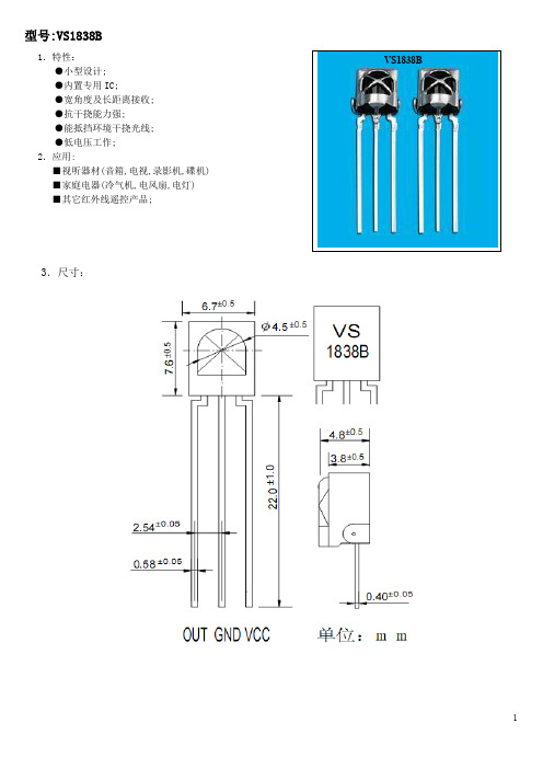
1.特性:
VS1838B
●小型设计;
●内置专用IC;
●宽角度及长距离接收;
●抗干挠能力强;
●能抵挡环境干挠光线;
●低电压工作;
2.应用:
■视听器材(音箱,电视,录影机,碟机)
■家庭电器(冷气机,电风扇,电灯)
■其它红外线遥控产品;
3.尺寸:
4.应用电路图:
5.原理图:
60
※光轴上测试,以宽度600/900μs为发射脉冲,在5CM之接收范围内,取50次接收脉冲之平均值。
7.测试波型:
8.特性曲线图(Characteristics Curve)(Tamb=25℃ unless otheruise specified):
Typical Electrical Curves at Temp=25℃
9
10
11.接收角度图:
12.使用注意:
1).在无任何外加压力及影响品质的环境下储存及使用;
2).在无污染气体或海风(含盐分)的环境下储存及使用;
3).在低湿度环境下储存及使用;
4).在规定的条件下焊接引线管脚,焊接后,请勿施加外力;
5).请勿清洗本产品,使用前,请先用静电带将作业员及电烙铁连接落地线;
6).请注意保护红外线接收器的接收面,沾污或磨损后会影响接收效果,同时不要触碰表面。
- 1、下载文档前请自行甄别文档内容的完整性,平台不提供额外的编辑、内容补充、找答案等附加服务。
- 2、"仅部分预览"的文档,不可在线预览部分如存在完整性等问题,可反馈申请退款(可完整预览的文档不适用该条件!)。
- 3、如文档侵犯您的权益,请联系客服反馈,我们会尽快为您处理(人工客服工作时间:9:00-18:30)。
亮彩系列标准格式转换器* 机图与实物图可能有细微差别,请以实物为准!接口说明:1、VOIP 接口。
流媒体IP 输入接口,可接计算机等提供输入信号。
2、10/100M 网络控制接口。
3、RS232控制接口。
用来进行上位机控制。
4、RS232控制接口。
用于多台设备级联。
5~6、HDMI 输入接口。
可接来自高清播放器、DVD 、计算机等的视频信号。
通过HDMI 接口输入信号;HDMI 输入为产品选配模块。
7~8、SDI 信号输入接口。
可接来自高清播放器、高清摄像机等的视频信号。
通过75欧姆匹配阻抗的BNC 头接入本设备7接口或8接口。
SDI 输入为产品选配模块。
9接口为SDI 环路输出接口,可接下一级的VSP 618或者具有SDI 输入接口的设备。
10~11、千兆网接口,通过网线连接LED 大屏幕。
12、发送卡电源接口,已经由视频处理器内部供电,不需要外部供电。
13、发送卡RS232控制接口。
14、DVI 输入接口,可直接与视频处理器的DVI 输出接口相连。
(此接口不支持热拔插)15~17、复合信号输入接口,同时兼容YCbCr(CV1(Y),CV2(Cb),CV3(Cr))信号。
可以接来自DVD 、机顶盒、硬盘播放器等的视频信号;通过75欧姆匹配阻抗的BNC头接入。
18、S 端子信号输入接口。
可接来自DVD 等的视频信号,通过S 端子接口输入信号;注意:VSP 618 基本配置包括接口 1~4、15~23、25~26、27~28。
VSP 618 B 除基本配置外还附SDI 输入模块,另配备接口、7、8、9。
VSP 618 C 除基本配置外还附HDMI 输入模块,另配备接口5、6。
VSP 618 D 除基本配置外还附HDMI 输出模块,另配备接口 24。
VSP 618 E 除基本配置外还附VOIP 模块,此模块安装在设备内部并未体现在产品图片中。
10~14为发送卡接口,非本设备标配模块。
20~22、分量信号输入接口。
可接来自DVD 播放器等的视频信号。
通过BNC×3接入本设备分量接口,从左到右依次为PR 、Y 、PB ;23、VGA 信号输入接口。
可接来自笔记本电脑等的视频信号。
通过VGA 接口接入本设备的VGA接口;24、HDMI 输出接口。
HDMI 输出为产品选配模块。
25、DVI 输出接口,可以接DVI 显示接口的显示器、LED 大屏幕控制卡等具有标准DVI 接口的设备。
(此接口不支持热拔插)26、VGA 输出接口。
输出信号可以接入显示器、投影仪等;27、开关及电源。
本设备使用标准的IEC-3电源线,确保设备可靠接地。
复合 BNC 输入输入接口数量:3支持标准:PAL/NTSC信号电平:1Vpp±3db (0.7V Video+0.3v Sync ) 75欧姆端结信号复用:YCbCrS-video DIN4输入输入接口数量:1支持标准:PAL/NTSC信号电平:Y:1Vpp±3dB (0.7V Video+0.3v Sync ) 75欧姆端结U/V:0.7Vpp±3dB 75欧姆端结前面板:后面板:19、DVI 信号输入接口。
可接来自电脑、DVI 信号发生器等的视频信号。
通过DVI 接口接入本设备DVI接口;(此接口不支持热拔插)DVI 输入输入接口数量: 1输入接口形态: 标准DVI-I 插座支持分辨率: SMPTE :625/25 PAL, 525/29.97 NTSC, 625/50p PAL, 525/59.94p NTSC, 1080i50,1080i59.94/60, 720p50 和 720p59.94/60VESA :800×600×60Hz ,1024×768×60Hz ,1280×768×60Hz ,1280×1024×60Hz ,1600×1200×60Hz ,1920×1080×60Hz ,1920×1080×50Hz信号电平:TMDS 电平,单像素输入,165MHz 带宽标准(Standard )DVI 1.1SDI 输入 (注意:SDI 输入为产品选配模块)输入接口数量: 2接口形态: BNC数据数率: 19.4Mbps~1.5Gbps支持标准:ITU-R BT.656,ITU-R BT.601,SMPTE 259M, SMPTE 292, SMPTE 297均衡(Equalization )Belden 1694A 200m 自适应高清1.485G ,350m 自适应标清270MbpsHDMI 输入 (注意:HDMI 输入为产品选配模块)输入接口数量: 2输入接口形态: HDMI 标准A 型接口支持分辨率:SMPTE :625/25 PAL, 525/29.97 NTSC, 625/50p PAL, 525/59.94p NTSC, 1080i50, 1080i59.94/60, 720p50 和 720p59.94/60VESA :800×600×60Hz ,1024×768×60Hz ,1280×768×60Hz ,1280×1024×60Hz ,1600×1200×60Hz ,1920×1080×60Hz ,1920×1080×50Hz信号电平: 电平,单像素输入,165MHz 带宽标准(Standard )HDMI 1.3SDI 环路输出 (注意:SDI 环路输出为产品选配模块)环路输出口数量: 1信号电平: 800mV±10%直流偏置: 0V±0.5V上升沿和下降沿: 高清1.485Gbps<270 ps ;标清270 Mbps 0.4 ns 到1.5ns过冲: <10%幅度时序抖动: 标清<0.2UI ;高清<1.0UI抖动校准: <0.2UIYPbPr BNC 输入输入接口数量: BNC*3支持标准: 模拟高清输入信号电平: Y:1Vpp±3dB (0.7V Video+0.3v Sync ) 75欧姆端结Pb/Pr:0.7Vpp±3dB 75欧姆端结VGA DB15输入输入接口数量: 1接口形态: 标准DB15插座支持分辨率: VGA-UXGA信号电平: R 、G 、B 、Hsync 、Vsync:0 to1Vpp±3dB (0.7V Video+0.3v Sync ) 75欧姆端结black level :300mV Sync-tip :0VDVI 输出输出接口数量: 1接口形态: 标准DVI-I 型接口输出支持分辨率:800×600×60Hz ,1024×768×60Hz ,1024×768×75Hz ,1280×768×60Hz ,1280×1024×60Hz 1440×900×60Hz ,1400×1200×60Hz ,1600×1200×60Hz ,1920×1080×60Hz ,1920×1200×60Hz ,2048×1152×60Hz 信号电平(Signal Level)TMDS 电平,165MHz 带宽HDMI 输出(注意:HDMI 输出为产品选配模块)输出接口数量:1输出接口形态:HDMI 标准A 型接口输出支持分辨率:800×600×60Hz ,1024×768×60Hz ,1024×768×75Hz ,1280×768×60Hz ,1280×1024×60Hz ,1440×900×60Hz ,1400×1200×60Hz ,1600×1200×60Hz ,1920×1080×60Hz ,1920×1200×60Hz2048×1152×60Hz信号电平(Signal Level)TMDS 电平,165MHz 带宽功能说明输入通道快捷键:支持每路信号快捷键操作PIP 双画面切换(PIP ):支持SD 与HD /HD 与HD 进行PIP亮键:支持设置控制:RS232 TCP/IP电源:85-264V 2A IEC-3电源接口工作环境:0°C~45°C储藏环境:10% to 90%产品质保:1年有限质保其他:VGA 输出输出接口数量:1接口形态:标准DB15插座输出支持分辨率:800×600×60Hz ,1024×768×60Hz ,1024×768×75Hz ,1280×768×60Hz ,1280×1024×60Hz ,1440×900×60Hz 1400×1200×60Hz ,1600×1200×60Hz ,1920×1080×60Hz ,1920×1200×60Hz ,2048×1152×60Hz ,2048×1536×60Hz信号电平:R 、G 、B 、Hsync 、Vsync:0 to1Vpp±3dB (0.7V Video+0.3v Sync ) 75欧姆端结black level :300mV Sync-tip :0V联系视诚厦门视诚科技有限公司厦门市湖里区留学人员创业园伟业楼S603电话: +86-592-5771197 传真:+86-592-5771202网站: E-mail :rgblinkcs@附录:亮彩系列视频处理器对照表。