EE-SX1108中文资料
EE-SX1131中文数据手册
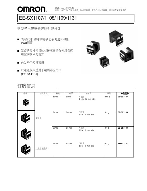
EE-SX1107/1108/1109/1131
微型光电传感器表贴封装设计
s 表贴设计, 磁带和卷轴包装促进自动化 PCB组装
s 紧凑的尺寸使得这些传感器适合使用在应 用空间受限的地方
s 高分辩率光电输出
直径. 80.0±1.0
(3.50)
直径 330.0±2.0
(13.00)
标签
带条 图1
E
K
C
A
0.3 (0.01) h
m n
12.4+00.2 (0.49) 18.4 max. (0.73)
4.0 (0.16)
直径. 1.5 1.75 (0.07) (0.06)
5.5 (0.22)
综合
光电流 (集电极电流)
集电极-发射极 饱和电压 上升时间 下降时间
注: 下面示图展示了上升时间 (tr) 与下降时间 (tf).
输入
输出
90%
10% tr
输入 t
tf
t
EE-SX1107/1108/1109/1131
符号 IF IFP VR VCEO VECO IC PC Topr Tstg Tsol Tsol
2.0 (0.08)
3.0 (0.12)
1.0 (0.04)
2.0 (0.08)
0.4 (0.02)
注: 1. 除非另有规定,公差±0.15毫米. 2. 括号内的值是相对应的英制尺寸.
引脚分配
C A
E1 NC
K E2
A 正极 NC 未连接 K 负极 C 集电极 E1 发射极 1 E2 发射极 2
EE-SPX304-W2A中文资料(omron)中文数据手册「EasyDatasheet - 矽搜」
Extension cable
避免从微型光电断开时电源被提供给微型光电或微型光电可
能会损坏.
如果金属安装基座进行感性电
噪音,可微型光电被意外激活.如果 噪音是个问题,采取以下预防措施:
1. GND端子连接到安装基座,于是就有 是在微型光电和安装基座之间电势没有差别.
2.通过GND端子连接到安装基座
0.47- µF电容.
间距d(毫米)
在TR上
Dark-ON mode
在TR上
Dark-ON mode
EE-SPX305-W2 d A
d
注:EE-SPX405-W2A检测位置特性是相反那
些EE-SPX305-W2A.
TR关闭
间距d(毫米)
TR关闭
间距d(毫米)
操作
J 内部/外部接线图
光时 ON /遮光时 ON
Operation indicator
零件号
EE-SPX302-W2A EE-SPX402-W2A EE-SPX304-W2A EE-SPX404-W2A EE-SPX305-W2A EE-SPX405-W2A EE-SPX306-W2A EE-SPX406-W2A
1
芯片中文手册,看全文,戳
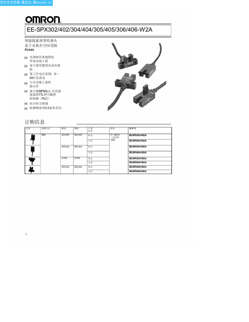
EE- -SPX302/402/304/404/305/405/306/406- -W2A
20 (0.79)
6.95(0.27)
14.5 (0.57)
1000±30
端子配置
红色(褐色)V CC
白色(黑色)输出
黑(蓝色)GND(0V)
IEC colors are shown in parentheses.
4
芯片中文手册,看全文,戳
EE- -SPX302/402/304/404/305/405/306/406- -W2A
MAX13085EESA-T中文资料

General DescriptionThe MAX13080E–MAX13089E +5.0V, ±15kV ESD-protect-ed, RS-485/RS-422 transceivers feature one driver and one receiver. These devices include fail-safe circuitry,guaranteeing a logic-high receiver output when receiver inputs are open or shorted. The receiver outputs a logic-high if all transmitters on a terminated bus are disabled (high impedance). The MAX13080E–MAX13089E include a hot-swap capability to eliminate false transitions on the bus during power-up or hot insertion.The MAX13080E/MAX13081E/MAX13082E feature reduced slew-rate drivers that minimize EMI and reduce reflections caused by improperly terminated cables, allowing error-free data transmission up to 250kbps. The MAX13083E/MAX13084E/MAX13085E also feature slew-rate-limited drivers but allow transmit speeds up to 500kbps. The MAX13086E/MAX13087E/MAX13088E driver slew rates are not limited, making transmit speeds up to 16Mbps possible. The MAX13089E slew rate is pin selectable for 250kbps,500kbps, and 16Mbps.The MAX13082E/MAX13085E/MAX13088E are intended for half-duplex communications, and the MAX13080E/MAX13081E/MAX13083E/MAX13084E/MAX13086E/MAX13087E are intended for full-duplex communica-tions. The MAX13089E is selectable for half-duplex or full-duplex operation. It also features independently programmable receiver and transmitter output phase through separate pins.The MAX13080E–MAX13089E transceivers draw 1.2mA of supply current when unloaded or when fully loaded with the drivers disabled. All devices have a 1/8-unit load receiver input impedance, allowing up to 256transceivers on the bus.The MAX13080E/MAX13083E/MAX13086E/MAX13089E are available in 14-pin PDIP and 14-pin SO packages.The MAX13081E/MAX13082E/MAX13084E/MAX13085E/MAX13087E/MAX13088E are available in 8-pin PDIP and 8-pin SO packages. The devices operate over the com-mercial, extended, and automotive temperature ranges.ApplicationsUtility Meters Lighting Systems Industrial Control Telecom Security Systems Instrumentation ProfibusFeatures♦+5.0V Operation♦Extended ESD Protection for RS-485/RS-422 I/O Pins±15kV Human Body Model ♦True Fail-Safe Receiver While Maintaining EIA/TIA-485 Compatibility ♦Hot-Swap Input Structures on DE and RE ♦Enhanced Slew-Rate Limiting Facilitates Error-Free Data Transmission(MAX13080E–MAX13085E/MAX13089E)♦Low-Current Shutdown Mode (Except MAX13081E/MAX13084E/MAX13087E)♦Pin-Selectable Full-/Half-Duplex Operation (MAX13089E)♦Phase Controls to Correct for Twisted-Pair Reversal (MAX13089E)♦Allow Up to 256 Transceivers on the Bus ♦Available in Industry-Standard 8-Pin SO PackageMAX13080E–MAX13089E+5.0V , ±15kV ESD-Protected, Fail-Safe, Hot-Swap, RS-485/RS-422 Transceivers________________________________________________________________Maxim Integrated Products 1Ordering Information19-3590; Rev 1; 4/05For pricing, delivery, and ordering information,please contact Maxim/Dallas Direct!at 1-888-629-4642, or visit Maxim’s website at .Selector Guide, Pin Configurations, and Typical Operating Circuits appear at end of data sheet.Ordering Information continued at end of data sheet.M A X 13080E –M A X 13089E+5.0V , ±15kV ESD-Protected, Fail-Safe, Hot-Swap, RS-485/RS-422 Transceivers 2_______________________________________________________________________________________ABSOLUTE MAXIMUM RATINGSDC ELECTRICAL CHARACTERISTICS(V CC = +5.0V ±10%, T A = T MIN to T MAX , unless otherwise noted. Typical values are at V CC = +5.0V and T A = +25°C.) (Note 1)Stresses beyond those listed under “Absolute Maximum Ratings” may cause permanent damage to the device. These are stress ratings only, and functional operation of the device at these or any other conditions beyond those indicated in the operational sections of the specifications is not implied. Exposure to absolute maximum rating conditions for extended periods may affect device reliability.(All Voltages Referenced to GND)Supply Voltage (V CC ).............................................................+6V Control Input Voltage (RE , DE, SLR,H/F , TXP, RXP)......................................................-0.3V to +6V Driver Input Voltage (DI)...........................................-0.3V to +6V Driver Output Voltage (Z, Y, A, B).............................-8V to +13V Receiver Input Voltage (A, B)....................................-8V to +13V Receiver Input VoltageFull Duplex (A, B)..................................................-8V to +13V Receiver Output Voltage (RO)....................-0.3V to (V CC + 0.3V)Driver Output Current.....................................................±250mAContinuous Power Dissipation (T A = +70°C)8-Pin SO (derate 5.88mW/°C above +70°C).................471mW 8-Pin Plastic DIP (derate 9.09mW/°C above +70°C).....727mW 14-Pin SO (derate 8.33mW/°C above +70°C)...............667mW 14-Pin Plastic DIP (derate 10.0mW/°C above +70°C)...800mW Operating Temperature RangesMAX1308_EC_ _.................................................0°C to +75°C MAX1308_EE_ _..............................................-40°C to +85°C MAX1308_EA_ _............................................-40°C to +125°C Junction Temperature......................................................+150°C Storage Temperature Range.............................-65°C to +150°C Lead Temperature (soldering, 10s).................................+300°CMAX13080E–MAX13089E+5.0V , ±15kV ESD-Protected, Fail-Safe, Hot-Swap, RS-485/RS-422 Transceivers_______________________________________________________________________________________3DC ELECTRICAL CHARACTERISTICS (continued)(V CC = +5.0V ±10%, T A = T MIN to T MAX , unless otherwise noted. Typical values are at V CC = +5.0V and T A = +25°C.) (Note 1)M A X 13080E –M A X 13089E+5.0V , ±15kV ESD-Protected, Fail-Safe, Hot-Swap, RS-485/RS-422 Transceivers 4_______________________________________________________________________________________DRIVER SWITCHING CHARACTERISTICSMAX13080E/MAX13081E/MAX13082E/MAX13089E WITH SRL = UNCONNECTED (250kbps)(V CC = +5.0V ±10%, T A = T MIN to T MAX , unless otherwise noted. Typical values are at V CC = +5.0V and T A = +25°C.)RECEIVER SWITCHING CHARACTERISTICSMAX13080E/MAX13081E/MAX13082E/MAX13089E WITH SRL = UNCONNECTED (250kbps)(V CC = +5.0V ±10%, T A = T MIN to T MAX , unless otherwise noted. Typical values are at V CC = +5.0V and T A = +25°C.)MAX13080E–MAX13089E+5.0V , ±15kV ESD-Protected, Fail-Safe, Hot-Swap, RS-485/RS-422 Transceivers_______________________________________________________________________________________5DRIVER SWITCHING CHARACTERISTICSMAX13083E/MAX13084E/MAX13085E/MAX13089E WITH SRL = V CC (500kbps)(V CC = +5.0V ±10%, T A = T MIN to T MAX , unless otherwise noted. Typical values are at V CC = +5.0V and T A = +25°C.)RECEIVER SWITCHING CHARACTERISTICSMAX13083E/MAX13084E/MAX13085E/MAX13089E WITH SRL = V CC (500kbps)(V CC = +5.0V ±10%, T A = T MIN to T MAX , unless otherwise noted. Typical values are at V CC = +5.0V and T A = +25°C.)M A X 13080E –M A X 13089E+5.0V , ±15kV ESD-Protected, Fail-Safe, Hot-Swap, RS-485/RS-422 Transceivers 6_______________________________________________________________________________________DRIVER SWITCHING CHARACTERISTICSMAX13086E/MAX13087E/MAX13088E/MAX13089E WITH SRL = GND (16Mbps)(V CC = +5.0V ±10%, T A = T MIN to T MAX , unless otherwise noted. Typical values are at V CC = +5.0V and T A = +25°C.)RECEIVER SWITCHING CHARACTERISTICSMAX13086E/MAX13087E/MAX13088E/MAX13089E WITH SRL = GND (16Mbps)(V CC = +5.0V ±10%, T A = T MIN to T MAX , unless otherwise noted. Typical values are at V CC = +5.0V and T A = +25°C.)Note 2:∆V OD and ∆V OC are the changes in V OD and V OC , respectively, when the DI input changes state.Note 3:The short-circuit output current applies to peak current just prior to foldback current limiting. The short-circuit foldback outputcurrent applies during current limiting to allow a recovery from bus contention.MAX13080E–MAX13089E+5.0V , ±15kV ESD-Protected, Fail-Safe, Hot-Swap, RS-485/RS-422 Transceivers_______________________________________________________________________________________70.800.901.501.101.001.201.301.401.60-40-10520-253550958011065125SUPPLY CURRENT vs. TEMPERATURETEMPERATURE (°C)S U P P L Y C U R R E N T (m A )0201040305060021345OUTPUT CURRENTvs. RECEIVER OUTPUT-HIGH VOLTAGEM A X 13080E -89E t o c 02OUTPUT HIGH VOLTAGE (V)O U T P U T C U R R E N T (m A )20104030605070021345OUTPUT CURRENTvs. RECEIVER OUTPUT-LOW VOLTAGEM A X 13080E -89E t o c 03OUTPUT LOW VOLTAGE (V)O U T P U T C U R R E N T (m A )4.04.44.24.84.65.25.05.4RECEIVER OUTPUT-HIGH VOLTAGEvs. TEMPERATURETEMPERATURE (°C)O U T P U T H I G H V O L T A G E (V )-40-10520-2535509580110651250.10.70.30.20.40.50.60.8RECEIVER OUTPUT-LOW VOLTAGEvs. TEMPERATURETEMPERATURE (°C)O U T P U T L O W V O L T A G E (V )-40-10520-25355095801106512502040608010012014016012345DRIVER DIFFERENTIAL OUTPUT CURRENT vs. DIFFERENTIAL OUTPUT VOLTAGEDIFFERENTIAL OUTPUT VOLTAGE (V)D I F FE R E N T I A L O U T P U T C U R R E N T (m A )2.02.82.43.63.24.44.04.8DRIVER DIFFERENTIAL OUTPUT VOLTAGE vs. TEMPERATURED I F FE R E N T I A L O U T P U T V O L T A G E (V )-40-10520-253550958011065125TEMPERATURE (°C)40201008060120140180160200-7-5-4-6-3-2-1012354OUTPUT CURRENT vs. TRANSMITTEROUTPUT-HIGH VOLTAGEOUTPUT HIGH VOLTAGE (V)O U T P U T C U R R E N T (m A )60402080100120140160180200042681012OUTPUT CURRENT vs. TRANSMITTEROUTPUT-LOW VOLTAGEOUTPUT-LOW VOLTAGE (V)O U T P U T C U R R E N T (m A )Typical Operating Characteristics(V CC = +5.0V, T A = +25°C, unless otherwise noted.)M A X 13080E –M A X 13089E+5.0V , ±15kV ESD-Protected, Fail-Safe, Hot-Swap, RS-485/RS-422 Transceivers 8_______________________________________________________________________________________21543679810SHUTDOWN CURRENT vs. TEMPERATUREM A X 13080E -89E t o c 10S H U T D O W N C U R R E N T (µA )-40-10520-253550958011065125TEMPERATURE (°C)600800700100090011001200DRIVER PROPAGATION DELAY vs. TEMPERATURE (250kbps)D R I VE R P R O P A G A T I O N D E L A Y (n s )-40-10520-253550958011065125TEMPERATURE (°C)300400350500450550600DRIVER PROPAGATION DELAY vs. TEMPERATURE (500kbps)D R I VE R P R O P A G A T I O N D E L A Y (n s )-40-10520-253550958011065125TEMPERATURE (°C)1070302040506080DRIVER PROPAGATION DELAY vs. TEMPERATURE (16Mbps)D R I VE R P R O P A G A T I O N D E L A Y (n s )-40-10520-253550958011065125TEMPERATURE (°C)40201008060120140160180RECEIVER PROPAGATION DELAYvs. TEMPERATURE (250kpbs AND 500kbps)R E C E I V E R P R O P A G A T I O N D E L A Y (n s )-40-10520-253550958011065125TEMPERATURE (°C)40201008060120140160180RECEIVER PROPAGATION DELAYvs. TEMPERATURE (16Mbps)R EC E I V E R P R O P A G AT I O N D E L A Y (n s )-40-10520-253550958011065125TEMPERATURE (°C)2µs/div DRIVER PROPAGATION DELAY (250kbps)DI 2V/divV Y - V Z 5V/divR L = 100Ω200ns/divRECEIVER PROPAGATION DELAY(250kbps AND 500kbps)V A - V B 5V/divRO 2V/divTypical Operating Characteristics (continued)(V CC = +5.0V, T A = +25°C, unless otherwise noted.)MAX13080E–MAX13089E+5.0V , ±15kV ESD-Protected, Fail-Safe, Hot-Swap, RS-485/RS-422 Transceivers_______________________________________________________________________________________9Test Circuits and Waveforms400ns/divDRIVER PROPAGATION DELAY (500kbps)DI 2V/divR L = 100ΩV Y - V Z 5V/div10ns/div DRIVER PROPAGATION DELAY (16Mbps)DI 2V/divR L = 100ΩV Y 2V/divV Z 2V/div40ns/divRECEIVER PROPAGATION DELAY (16Mbps)V B 2V/divR L = 100ΩRO 2V/divV A 2V/divTypical Operating Characteristics (continued)(V CC = +5.0V, T A = +25°C, unless otherwise noted.)Figure 2. Driver Timing Test CircuitM A X 13080E –M A X 13089E+5.0V , ±15kV ESD-Protected, Fail-Safe, Hot-Swap, RS-485/RS-422 Transceivers 10______________________________________________________________________________________Test Circuits and Waveforms (continued)Figure 4. Driver Enable and Disable Times (t DHZ , t DZH , t DZH(SHDN))DZL DLZ DLZ(SHDN)MAX13080E–MAX13089E+5.0V , ±15kV ESD-Protected, Fail-Safe, Hot-Swap, RS-485/RS-422 TransceiversTest Circuits and Waveforms (continued)Figure 6. Receiver Propagation Delay Test CircuitM A X 13080E –M A X 13089E+5.0V , ±15kV ESD-Protected, Fail-Safe, Hot-Swap, RS-485/RS-422 TransceiversMAX13080E–MAX13089E+5.0V , ±15kV ESD-Protected, Fail-Safe, Hot-Swap, RS-485/RS-422 TransceiversMAX13080E/MAX13083E/MAX13086EMAX13081E/MAX13084E/MAX13086E/MAX13087EFunction TablesM A X 13080E –M A X 13089E+5.0V , ±15kV ESD-Protected, Fail-Safe, Hot-Swap, RS-485/RS-422 Transceivers MAX13082E/MAX13085E/MAX13088EFunction Tables (continued)MAX13089EDetailed Description The MAX13080E–MAX13089E high-speed transceivers for RS-485/RS-422 communication contain one driver and one receiver. These devices feature fail-safe circuit-ry, which guarantees a logic-high receiver output when the receiver inputs are open or shorted, or when they are connected to a terminated transmission line with all dri-vers disabled (see the Fail-Safe section). The MAX13080E/MAX13082E/MAX13083E/MAX13085E/ MAX13086E/MAX13088E/MAX13089E also feature a hot-swap capability allowing line insertion without erroneous data transfer (see the Hot Swap Capability section). The MAX13080E/MAX13081E/MAX13082E feature reduced slew-rate drivers that minimize EMI and reduce reflec-tions caused by improperly terminated cables, allowing error-free data transmission up to 250kbps. The MAX13083E/MAX13084E/MAX13085E also offer slew-rate limits allowing transmit speeds up to 500kbps. The MAX13086E/MAX13087E/MAX13088Es’ driver slew rates are not limited, making transmit speeds up to 16Mbps possible. The MAX13089E’s slew rate is selectable between 250kbps, 500kbps, and 16Mbps by driving a selector pin with a three-state driver.The MAX13082E/MAX13085E/MAX13088E are half-duplex transceivers, while the MAX13080E/MAX13081E/ MAX13083E/MAX13084E/MAX13086E/MAX13087E are full-duplex transceivers. The MAX13089E is selectable between half- and full-duplex communication by driving a selector pin (H/F) high or low, respectively.All devices operate from a single +5.0V supply. Drivers are output short-circuit current limited. Thermal-shutdown circuitry protects drivers against excessive power dissi-pation. When activated, the thermal-shutdown circuitry places the driver outputs into a high-impedance state.Receiver Input Filtering The receivers of the MAX13080E–MAX13085E, and the MAX13089E when operating in 250kbps or 500kbps mode, incorporate input filtering in addition to input hysteresis. This filtering enhances noise immunity with differential signals that have very slow rise and fall times. Receiver propagation delay increases by 25% due to this filtering.Fail-Safe The MAX13080E family guarantees a logic-high receiver output when the receiver inputs are shorted or open, or when they are connected to a terminated transmission line with all drivers disabled. This is done by setting the receiver input threshold between -50mV and -200mV. If the differential receiver input voltage (A - B) is greater than or equal to -50mV, RO is logic-high. If (A - B) is less than or equal to -200mV, RO is logic-low. In the case of a terminated bus with all transmitters disabled, the receiv-er’s differential input voltage is pulled to 0V by the termi-nation. With the receiver thresholds of the MAX13080E family, this results in a logic-high with a 50mV minimumnoise margin. Unlike previous fail-safe devices, the-50mV to -200mV threshold complies with the ±200mVEIA/TIA-485 standard.Hot-Swap Capability (Except MAX13081E/MAX13084E/MAX13087E)Hot-Swap InputsWhen circuit boards are inserted into a hot or powered backplane, differential disturbances to the data buscan lead to data errors. Upon initial circuit board inser-tion, the data communication processor undergoes itsown power-up sequence. During this period, the processor’s logic-output drivers are high impedanceand are unable to drive the DE and RE inputs of these devices to a defined logic level. Leakage currents up to±10µA from the high-impedance state of the proces-sor’s logic drivers could cause standard CMOS enableinputs of a transceiver to drift to an incorrect logic level. Additionally, parasitic circuit board capacitance couldcause coupling of V CC or GND to the enable inputs. Without the hot-swap capability, these factors could improperly enable the transceiver’s driver or receiver.When V CC rises, an internal pulldown circuit holds DElow and RE high. After the initial power-up sequence,the pulldown circuit becomes transparent, resetting thehot-swap tolerable input.Hot-Swap Input CircuitryThe enable inputs feature hot-swap capability. At theinput there are two NMOS devices, M1 and M2 (Figure 9). When V CC ramps from zero, an internal 7µstimer turns on M2 and sets the SR latch, which alsoturns on M1. Transistors M2, a 1.5mA current sink, andM1, a 500µA current sink, pull DE to GND through a5kΩresistor. M2 is designed to pull DE to the disabledstate against an external parasitic capacitance up to100pF that can drive DE high. After 7µs, the timer deactivates M2 while M1 remains on, holding DE low against three-state leakages that can drive DE high. M1 remains on until an external source overcomes the required input current. At this time, the SR latch resetsand M1 turns off. When M1 turns off, DE reverts to a standard, high-impedance CMOS input. Whenever V CCdrops below 1V, the hot-swap input is reset.For RE there is a complementary circuit employing two PMOS devices pulling RE to V CC. MAX13080E–MAX13089E+5.0V, ±15kV ESD-Protected, Fail-Safe, Hot-Swap, RS-485/RS-422 TransceiversM A X 13080E –M A X 13089EMAX13089E ProgrammingThe MAX13089E has several programmable operating modes. Transmitter rise and fall times are programma-ble, resulting in maximum data rates of 250kbps,500kbps, and 16Mbps. To select the desired data rate,drive SRL to one of three possible states by using a three-state driver: V CC , GND, or unconnected. F or 250kbps operation, set the three-state device in high-impedance mode or leave SRL unconnected. F or 500kbps operation, drive SRL high or connect it to V CC .F or 16Mbps operation, drive SRL low or connect it to GND. SRL can be changed during operation without interrupting data communications.Occasionally, twisted-pair lines are connected backward from normal orientation. The MAX13089E has two pins that invert the phase of the driver and the receiver to cor-rect this problem. F or normal operation, drive TXP and RXP low, connect them to ground, or leave them uncon-nected (internal pulldown). To invert the driver phase,drive TXP high or connect it to V CC . To invert the receiver phase, drive RXP high or connect it to V CC . Note that the receiver threshold is positive when RXP is high.The MAX13089E can operate in full- or half-duplex mode. Drive H/F low, leave it unconnected (internal pulldown), or connect it to GND for full-duplex opera-tion. Drive H/F high for half-duplex operation. In full-duplex mode, the pin configuration of the driver and receiver is the same as that of a MAX13080E. In half-duplex mode, the receiver inputs are internally connect-ed to the driver outputs through a resistor-divider. This effectively changes the function of the device’s outputs.Y becomes the noninverting driver output and receiver input, Z becomes the inverting driver output and receiver input. In half-duplex mode, A and B are still connected to ground through an internal resistor-divider but they are not internally connected to the receiver.±15kV ESD ProtectionAs with all Maxim devices, ESD-protection structures are incorporated on all pins to protect against electro-static discharges encountered during handling and assembly. The driver outputs and receiver inputs of the MAX13080E family of devices have extra protection against static electricity. Maxim’s engineers have devel-oped state-of-the-art structures to protect these pins against ESD of ±15kV without damage. The ESD struc-tures withstand high ESD in all states: normal operation,shutdown, and powered down. After an ESD event, the MAX13080E–MAX13089E keep working without latchup or damage.ESD protection can be tested in various ways. The transmitter outputs and receiver inputs of the MAX13080E–MAX13089E are characterized for protec-tion to the following limits:•±15kV using the Human Body Model•±6kV using the Contact Discharge method specified in IEC 61000-4-2ESD Test ConditionsESD performance depends on a variety of conditions.Contact Maxim for a reliability report that documents test setup, test methodology, and test results.Human Body ModelFigure 10a shows the Human Body Model, and Figure 10b shows the current waveform it generates when dis-charged into a low impedance. This model consists of a 100pF capacitor charged to the ESD voltage of interest,which is then discharged into the test device through a 1.5k Ωresistor.IEC 61000-4-2The IEC 61000-4-2 standard covers ESD testing and performance of finished equipment. However, it does not specifically refer to integrated circuits. The MAX13080E family of devices helps you design equip-ment to meet IEC 61000-4-2, without the need for addi-tional ESD-protection components.+5.0V , ±15kV ESD-Protected, Fail-Safe, Hot-Swap, RS-485/RS-422 TransceiversThe major difference between tests done using the Human Body Model and IEC 61000-4-2 is higher peak current in IEC 61000-4-2 because series resistance is lower in the IEC 61000-4-2 model. Hence, the ESD with-stand voltage measured to IEC 61000-4-2 is generally lower than that measured using the Human Body Model. Figure 10c shows the IEC 61000-4-2 model, and Figure 10d shows the current waveform for IEC 61000-4-2 ESD Contact Discharge test.Machine Model The machine model for ESD tests all pins using a 200pF storage capacitor and zero discharge resis-tance. The objective is to emulate the stress caused when I/O pins are contacted by handling equipment during test and assembly. Of course, all pins require this protection, not just RS-485 inputs and outputs.Applications Information256 Transceivers on the BusThe standard RS-485 receiver input impedance is 12kΩ(1-unit load), and the standard driver can drive up to 32-unit loads. The MAX13080E family of transceivers has a1/8-unit load receiver input impedance (96kΩ), allowingup to 256 transceivers to be connected in parallel on one communication line. Any combination of these devices,as well as other RS-485 transceivers with a total of 32-unit loads or fewer, can be connected to the line.Reduced EMI and ReflectionsThe MAX13080E/MAX13081E/MAX13082E feature reduced slew-rate drivers that minimize EMI and reduce reflections caused by improperly terminated cables, allowing error-free data transmission up to250kbps. The MAX13083E/MAX13084E/MAX13085Eoffer higher driver output slew-rate limits, allowing transmit speeds up to 500kbps. The MAX13089E withSRL = V CC or unconnected are slew-rate limited. WithSRL unconnected, the MAX13089E error-free data transmission is up to 250kbps. With SRL connected toV CC,the data transmit speeds up to 500kbps. MAX13080E–MAX13089E+5.0V, ±15kV ESD-Protected, Fail-Safe, Hot-Swap, RS-485/RS-422 TransceiversM A X 13080E –M A X 13089ELow-Power Shutdown Mode (Except MAX13081E/MAX13084E/MAX13087E)Low-power shutdown mode is initiated by bringing both RE high and DE low. In shutdown, the devices typically draw only 2.8µA of supply current.RE and DE can be driven simultaneously; the devices are guaranteed not to enter shutdown if RE is high and DE is low for less than 50ns. If the inputs are in this state for at least 700ns, the devices are guaranteed to enter shutdown.Enable times t ZH and t ZL (see the Switching Characteristics section) assume the devices were not in a low-power shutdown state. Enable times t ZH(SHDN)and t ZL(SHDN)assume the devices were in shutdown state. It takes drivers and receivers longer to become enabled from low-power shutdown mode (t ZH(SHDN), t ZL(SHDN))than from driver/receiver-disable mode (t ZH , t ZL ).Driver Output ProtectionTwo mechanisms prevent excessive output current and power dissipation caused by faults or by bus contention.The first, a foldback current limit on the output stage,provides immediate protection against short circuits over the whole common-mode voltage range (see the Typical Operating Characteristics ). The second, a thermal-shut-down circuit, forces the driver outputs into a high-imped-ance state if the die temperature exceeds +175°C (typ).Line LengthThe RS-485/RS-422 standard covers line lengths up to 4000ft. F or line lengths greater than 4000ft, use the repeater application shown in Figure 11.Typical ApplicationsThe MAX13082E/MAX13085E/MAX13088E/MAX13089E transceivers are designed for bidirectional data commu-nications on multipoint bus transmission lines. F igures 12 and 13 show typical network applications circuits. To minimize reflections, terminate the line at both ends in its characteristic impedance, and keep stub lengths off the main line as short as possible. The slew-rate-lim-ited MAX13082E/MAX13085E and the two modes of the MAX13089E are more tolerant of imperfect termination.Chip InformationTRANSISTOR COUNT: 1228PROCESS: BiCMOS+5.0V , ±15kV ESD-Protected, Fail-Safe, Hot-Swap, RS-485/RS-422 TransceiversFigure 11. Line Repeater for MAX13080E/MAX13081E/MAX13083E/MAX13084E/MAX13086E/MAX13087E/MAX13089E in Full-Duplex Mode+5.0V, ±15kV ESD-Protected, Fail-Safe, Hot-Swap, RS-485/RS-422 TransceiversMAX13080E–MAX13089EM A X 13080E –M A X 13089E+5.0V , ±15kV ESD-Protected, Fail-Safe, Hot-Swap, RS-485/RS-422 TransceiversPin Configurations and Typical Operating CircuitsMAX13080E–MAX13089E+5.0V , ±15kV ESD-Protected, Fail-Safe, Hot-Swap, RS-485/RS-422 Transceivers______________________________________________________________________________________21Pin Configurations and Typical Operating Circuits (continued)M A X 13080E –M A X 13089E+5.0V , ±15kV ESD-Protected, Fail-Safe, Hot-Swap, RS-485/RS-422 Transceivers 22______________________________________________________________________________________Ordering Information (continued)MAX13080E–MAX13089E+5.0V , ±15kV ESD-Protected, Fail-Safe, Hot-Swap, RS-485/RS-422 Transceivers______________________________________________________________________________________23Package Information (continued)(The package drawing(s) in this data sheet may not reflect the most current specifications. For the latest package outline information,go to /packages .)。
EE-SX97
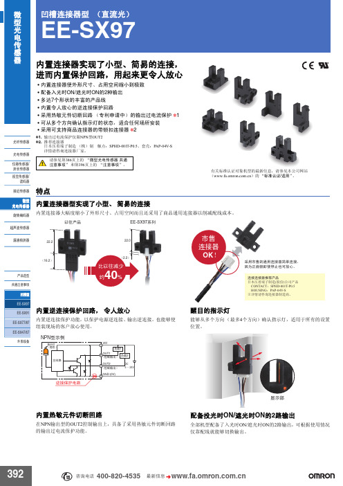
䞛⫼Ꮦଂⱘ䗮⫼䖲఼ㅔऩ䖲ˈ Ўℷ䴶䫕ेՓذℶгৃᬒᖗDŽ
䖲䖲఼㤤ѻક ᮹ᴀय़ⴔッᄤࠊ䗴(㙵ӑ)݀ৌѻક ǂCONTACT˖SPHD-001T-P0.5 ǂHOUSING˖PAP-04V-S Ć䆺ᚙ䇋䆶䖲఼ࠊ䗴ଚDŽ
EE-SX97 EE-SX91 EE-SX77/87 EE-SX47/67 ೈ䆒
(凹槽型) (4极)
EE-SX972-C1
入光时ON 5mm 遮光时ON 入光时点亮 ˄ῑᆑ˅ 配备2种输出
EE-SX974-C1
EE-SX975-C1
EE-SX976-C1
EE-SX972P-C1 EE-SX974P-C1 EE-SX975P-C1 EE-SX976P-C1
ܝ㑸Ӵᛳ఼
⬉ܝӴᛳ఼ ԡ鼠Ӵᛳ఼/ ⌟䭓Ӵᛳ఼ 㾚㾝Ӵᛳ఼/ 䇏ⷕ఼ 䖥Ӵᛳ఼ ᖂൟ ⬉ܝӴᛳ఼ ᮟ䕀㓪ⷕ఼
振动 (耐久)
10~2,000Hz 单振幅0.75mm X、 Y、 Z各方向 扫描时间:15分钟 扫描次数:10次
冲击 (耐久)
500m/s2 X、 Y、 Z各方向 3次
ᖂ ൟ
凹槽连接器型 (直流光)
ܝ ⬉ Ӵ
EE-SX97
ᛳ
఼
内置连接器实现了小型、简易的连接,
进而内置保护回路,用起来更令人放心
ܝ㑸Ӵᛳ఼
⬉ܝӴᛳ఼
ԡ鼠Ӵᛳ఼/ ⌟䭓Ӵᛳ఼ 㾚㾝Ӵᛳ఼/
䇏ⷕ఼
䖥Ӵᛳ఼
• 内置连接器使外形尺寸、占用空间缩小到极致 • 配备入光时ON/遮光时ON的2种输出 • 多达7个形状的丰富的产品线 • 内置令人放心的逆连接保护回路 • 采用热敏元件切断回路 (专利申请中)的输出过电流保护 *1 • 可从多个方向确认指示灯的状态,适合任何场所安装 • 采用可支持商品连接器的带锁扣连接器 *2
EE-SX911-R 1M;中文规格书,Datasheet资料

Sensing distance Sensing object Differential distance Light source Indicator Supply voltage Current consumption
Control output
Protection circuits Response frequency Ambient illumination Ambient temperature range Ambient humidity range Vibration resistance (Destruction) Shock resistance (Destruction) Degree of protection Connecting method
Байду номын сангаас
Indicator Visible from Many Directions for Installation in Any Location Compact NPN and PNP Output Models
Both NPN and PNP output models are available for use according to system requirements. The light indicator can be checked from up to four directions.
Compact Pre-wired Photomicrosensor with Built-in Amplifier (Non-modulated)
EE-SX91
CSM_EE-SX91_DS_E_3_1
Meeting Customer Needs with Compact Sensors that Mount with M3 Screws
32 EE-SX1108 照明传感器(透射)商品说明书

8■DimensionsNote:All units are in millimeters unless otherwise indicated.■Features•Ultra-compact with a 5-mm-wide sensor and a 2-mm-wide slot.•PCB surface mounting type.•High resolution with a 0.3-mm-wide aperture.■Absolute Maximum Ratin g s (Ta =25°C)Note:1.Refer to the temperature rating chart if the ambient temper-ature exceeds 25°C.2.Duty: 1/100; Pulse width: 0.1 msplete soldering within 10 seconds for reflow soldering and within 3 seconds for manual soldering.■Electrical and Optical Characteristics (Ta = 25°C)Internal CircuitTerminal No. Name A Anode K Cathode C Collector EEmitterCross section AAOptical axisRecommended Solderin g PatternUnless otherwise specified, the tolerances are ±0.15 mm.ItemSymbol Rated value EmitterForward current I F 25 mA(see note 1)Pulse forward cur-rentI FP 100 mA (see note 2)Reverse volta g eV R 5 V DetectorCollector–Emitter volta g eV CEO 20 V Emitter–Collector volta g eV ECO 5 V Collector currentI C 20 mA Collector dissipa-tionP C 75 mW (see note 1)Ambient tem-peratureOperatin g T opr –30°C to 85°C Stora g eTstg –40°C to 90°C Reflow solderin gTsol 255°C(see note 3)Manual solderin gTsol350°C(see note 3)ItemSymbolValueConditionEmitterForward volta g e V F 1.1 V typ., 1.3 V max.I F = 5 mA Reverse currentI R 10 μA max.V R = 5 V Peak emission wavelen g thλP 940 nm typ.I F = 20 mADetectorLi g ht current I L 50 μA min., 150 μA typ., 500 μA max.I F = 5 mA, V CE = 5 V Dark current I D 100 nA max.V CE = 10 V , 0 l x Leaka g e currentI LEAK ------Collector–Emitter saturated volta g e V CE (sat)0.1 V typ., 0.4 V max.I F = 20 mA, I L = 50 μA Peak spectral sensitivity wavelen g thλP 900 nm typ.---Risin g time tr 10 μs typ.V CC = 5 V , R L = 1 k Ω,I L = 100μAFallin g timetf10 μs typ.V CC = 5 V , R L = 1 k Ω,I L = 100μABe sure to read Precautions on pa g e 24.■En g ineerin g DataForward Current vs. Collector Dissipation Temperature Ratin gForward Current vs. Forward Volta g e Characteristics (Typical)Li g ht Current vs. Forward Current Characteristics (Typical)Li g ht Current vs. Collector −Emitter Volta g e Characteristics (Typical)Relative Li g ht Current vs. Ambient Temperature Characteristics (Typical)Dark Current vs. Ambient Tem-perature Characteristics (Typical)Distance d (mm)Input OutputInputOutput90 %10 %Sensin g Position Characteristics (Typical)Response Time Measurement CircuitDistance d (mm)Sensin g Position Characteristics (Typical)V CE = 2 VAmbient temperature T a (°C)C o l l e c t o r d i s s i p a t i o n P C (m W )Forward voltage V F (V)F o r w a r d c u r r e n t I F (m A )F o r w a r d c u r r e n t I F (m A )Forward current I F (mA)L i g h t c u r r e n t I L (μA )Collector −Emitter voltage V CE (V)L i g h t c u r r e n t I L (μA )Ambient temperature Ta (°C)Load resistance R L (k Ω)Ta = 25°C V CE = 5 VI F = 10 mAI F = 5 mAT a = 25°CI F = 5 mAV CE = 5 VI F = 5 mA V CE = 5 VV CC = 5 V Ta = 25°CR e s p o n s e t i m e t r , t f (μs )R e l a t i v e l i g h t c u r r e n t I L (%)D a r k c u r r e n t I D (n A )R e l a t i v e l i g h t c u r r e n t I L (%)Ambient temperature Ta (°C)R e l a t i v e l i g h t c u r r e n t I L (%)I F = 5 mA V CE = 5 VResponse Time vs. Load Resist-ance Characteristics (Typical)V CE = 10 VUnit: mm (inch)■Tape and Reel ReelTapeTape confi g uration Tape quantity2,000 pcs./reel21±0.8 dia.2±0.513±0.5 dia.Product nameQuantityLot number80±1 dia.330±2 dia.12.4+2018.4 max.1.5 dia.Terminating part(40 mm min.)Pull-out directionEmpty(40 mm min.)Parts mounted Leading part(400 mm min.)Precautions■Solderin g InformationReflow solderin g•The following soldering paste is recommended:Melting temperature: 216 to 220°CComposition: Sn 3.5 Ag 0.75 Cu•The recommended thickness of the metal mask for screen printing is between 0.2 and 0.25 mm.•Set the reflow oven so that the temperature profile shown in the following chart is obtained for the upper surface of the product being soldered.Manual solderin g•Use ”Sn 60” (60% tin and 40% lead) or solder with silver content.•Use a soldering iron of less than 25 W, and keep the temperature of the iron tip at 300°C or below.•Solder each point for a maximum of three seconds.•After soldering, allow the product to return to room temperature before handling it.Stora g eTo protect the product from the effects of humidity until the package is opened, dry-box storage is recommended. If this is not possible, store the product under the following conditions:Temperature: 10 to 30°CHumidity: 60% max.The product is packed in a humidity-proof envelope. Reflow soldering must be done within 48 hours after opening the envelope, during which time the product must be stored under 30°C at 80% maximum humidity.If it is necessary to store the product after opening the envelope, use dry-box storage or reseal the envelope.Bakin gIf a product has remained packed in a humidity-proof envelope for six months or more, or if more than 48 hours have lapsed since the envelope was opened, bake the product under the following conditions before use:Reel: 60°C for 24 hours or moreBulk: 80°C for 4 hours or more。
TESCOM中文样本

Cv = 1.3
• 可提供高精度的外部
PSIG
取压
• 平衡主阀设计增加了阀座寿命
26-1200 系列: 高流量
• 与上述 26-1100 类似
6,000 PSIG (414 Bar) 100-6,000 PSIG
更大的流量范围
Cv = 3.3 Cv =6.0 Cv = 12.0
0-1200, 0-1800
PSIG
铝 316 不锈钢
BB-5 系列: 袖珍型,两级减压
• 重量轻,设计紧凑
6,000 PSIG (414 Bar)
• 级间安全泄放接口
• 活塞感应,使用寿命长
• 无排放功能
0-80, 0-140,
Cv = 0.Байду номын сангаас6
0-220, 0-700,
0-1200 PSIG
• 设计紧凑
(414 Bar)
Cv = 0.24
• 挡块限制最大出口压力
• 入口及出口压力表接口为标配
• 标配无排放功能
黄铜 300 不锈钢 316 不锈钢
26-1000 多用途
26-1000 系列: 多用途
• 出口压力范围可
6,000 , 10,000 PSIG
现场调节
(414, 690 Bar)
• 多种接口选择
• 可选入口压力达
20,000 PSIG (1379 Bar)
• 大手柄设计,扭矩低
压力设定快速
• 标配带自排放功能
5-500, 5-800, 10-1500, 15-2500, 25-4000, 50-6000, 200-10,000 PSIG
Cv = 0.02 Cv = 0.06 Cv = 0.12 Cv = 0.3
分选仪用户手册-2.0版本

目
录
安全须知...........................................................................................................................................1 公司简介...........................................................................................................................................4 1. 概述.............................................................................................................................................5 1.1 使用对象........................................................................................................................... 5 1.2 测试仪的技术参数........................................................................................................... 5 1.3 工作环境..............................................................................................
EE-SX671;EE-SX674;EE-SX670A;EE-SX670P;EE-SX671A;中文规格书,Datasheet资料

T-shaped, slot center 10 mm F-shaped
Dark-ON/Light-ON Incident light (selectable) *3
EE-SX675
EE-SX675P
Dark-ON/Light-ON Incident light (selectable) *3 R-shaped Dark-ON/Light-ON Incident light (selectable) *3
EE-SX670 EE-SX671 EE-SX673 EE-SX674 Connector EE-SX675 EE-SX670A EE-SX671A EE-SX673A EE-SX674A models EE-SX470 EE-SX471 EE-SX473 EE-SX474 NPN Pre-wired EE-SX670EE-SX671EE-SX673EE-SX674EE-SX675models models WR WR WR WR WR Models with EE-SX670EE-SX671EE-SX673EE-SX674EE-SX675connectors CJ1-R CJ1-R CJ1-R CJ1-R CJ1-R EE-SX670P EE-SX671P EE-SX673P EE-SX674P Connector EE-SX670R EE-SX675P EE-SX671R EE-SX673R EE-SX674R models EE-SX470P EE-SX471P EE-SX473P EE-SX474P PNP Pre-wired EE-SX670PEE-SX671PEE-SX673PEE-SX674PEE-SX675Pmodels models WR WR WR WR WR Models with EE-SX670PEE-SX671PEE-SX673PEE-SX674PEE-SX675PItem connectors CJ1-R CJ1-R CJ1-R CJ1-R CJ1-R Sensing distance 5 mm (slot width) Sensing object Opaque: 2 × 0.8 mm min. Differential distance 0.025 mm Light source GaAs infrared LED with a peak wavelength of 940 nm Indicator *1 Light indicator (red) (turns ON when light is interrupted for models with A or R suffix) Supply voltage 5 to 24 VDC ±10%, ripple (p-p): 10% max. Current consumption 35 mA max. (NPN models), 30 mA max. (PNP models) NPN open collector: 5 to 24 VDC, 100 mA max. 100 mA load current with a residual voltage of 0.8 V max. 40 mA load current with a residual voltage of 0.4 V max. Control output OFF current: 0.5 mA max. PNP open collector: 5 to 24 VDC, 50 mA max. 50 mA load current with a residual voltage of 1.3 V max. OFF current: 0.5 mA max. Response frequency *2 1 kHz min. (3 kHz average) Ambient illumination 1,000 lx max. with fluorescent light on the surface of the receiver. Ambient temperature range Operating: −25 to +55°C, Storage: −30 to +80°C (with no icing or condensation) Ambient humidity range Operating: 5% to 85%, Storage: 5% to 95% (with no icing or condensation) Destruction: 20 to 2,000 Hz (peak acceleration: 100 m/s2) Vibration resistance 1.5-mm double amplitude for 2 h (4-min periods) each in X, Y, and Z directions Shock resistance Destruction: 500 m/s2 for 3 times each in X, Y, and Z directions Degree of protection IEC60529 IP50 Connector Models (direct soldering possible), Pre-wired Models (Standard cable length: 1 m), Connecting method Models with Connectors (Standard cable length: 0.1 m) Connector models Approx. 3.1 g Approx. 3 g Approx. 2.4 g Approx. 2.3 g Approx. 3 g Approx. 2.7 g Wei- Pre-wired models Approx. 18.9 g Approx. 17.3 g Approx. 17.8 g Approx. 16.8 g Approx. 17.1 g Approx. 18.3 g ght Models with Approx. 6.3 g Approx. 4.7 g Approx. 5.2 g Approx. 4.2 g Approx. 4.5 g Approx. 5.7 g connectors Case Polybutylene phthalate (PBT) Materi- Cover Polycarbonate al Emitter/receiver *1. The indicator is a GaP red LED (peak wavelength: 690 nm). *2. The response frequency was measured by detecting the rotating disk shown at the right.
HBS1108S 高压数字式简易伺服驱动器使用说明书
深圳市雷赛智能控制股份有限公司地址:深圳市南山区学苑大道1001号南山智园A3栋11楼邮编:518055电话:400-885-5521传真:*************Email:***************网址:上海分公司北京办事处地址:上海市淞江区九亭镇九新公路地址:北京市朝阳区北苑路13号院领地76号嘉和阳光大厦9楼office1号楼A单元606号电话:************电话:************传真:************传真:************HBS1108S高压数字式简易伺服驱动器使用说明书版权所有不得翻印【使用前请仔细阅读本手册,以免损坏驱动器】深圳市雷赛智能控制股份有限公司目录一、产品简介 (2)1.概述 (2)2.技术特点 (2)3.应用领域 (3)二、电气、机械和环境指标 (3)1.电气指标 (3)2.使用环境及参数 (3)3.机械安装图 (4)4.加强散热方式 (4)三、驱动器接口和接线介绍 (5)1.接口定义 (5)2.控制信号接口电路 (7)3.控制信号时序图 (8)4.控制信号模式及细分设置 (9)5.编码器接线 (9)四、驱动器参数设置 (9)五、典型应用接线 (13)1.简易伺服电机线定义 (14)2.带抱闸电机接线方法 (14)雷赛产品保修条款 (15)HBS1108S高压数字式简易伺服驱动器一、产品简介1、概述HBS1108S是雷赛公司基于十几年步进与伺服研发经验开发成功的一款新型简易伺服驱动器,采用最新专用电机控制DSP芯片和应用矢量型闭环控制技术,从而彻底克服开环步进电机丢步的问题,同时也能明显提升电机的高速性能、降低电机的发热程度和减小电机的振动,从而提升机器的加工速度和精度以及降低机器的能耗。
此外,在电机连续过载时,驱动器会输出报警信号,具有与交流伺服系统同样的可靠性。
HBS1108S适配电机安装尺寸与传统的86系列步进电机完全兼容,传统步进驱动方案极易升级,并且成本仅相当于传统交流伺服系统的50%。
UL1082-中文版

5.2 壳体材料应能适合于特定的应用要求,能将使用时可能引发火灾,电击或伤害人体的所有电气零件(电 源线除外)封闭起来。
5.3 判断壳体是否适用于特定的应用要求,其考虑因素有: (1) 机械强度; (2) 抗冲击性能; (3) 吸湿性能; (4) 燃烧性; (5) 耐腐蚀性能; (6) 在正常使用或非正常使用温度下壳体的抗变形性能。 对非金属材料壳体,见 UL 746C Standard for Polymeric Materials — Use in Electrical Equipment Evaluation 的壳体要求。金属材料壳体,按 34 章试验来检查其冲击性能。
流电压为 42.4V)。如果输入电路用串联阻抗来分压限流,再连接到线电压电路上,则该输入电路不 是低压电路,也不是隔离限压次级电路。见 11A.5。
版权所有人:TOMS.XU
未经许可,严禁拷贝 !
投诉电话:0755-86027268
HOUSEHOLD ELECTRIC COFFEE MAKERS AND BREWING-TYPE APPLIANCES – UL 1082(家用电咖啡壶及酿造类器具)
5.8 壳体结构应使得熔融金属,绝缘材料的燃烧,火花等不会落下到支撑表面上。
5.9 为满足 5.8 节的要求,对于底部开孔的壳体,如为下列情况,必须在孔位上方或下方加挡板: A. 位于马达下方,但以下情况除外:
1. 马达或器具的结构零件已有等同功能的挡板。
2. 马达带保护装置,使得当马达在下列故障情况下通电时,没有绝缘材料燃烧颗粒或熔融金 属落到器具支撑表面上:
2
31. 高压测试
29
32. 断开发热丝测试
29
33. 电源线拉力测试
30
Omron光电开关资料(EE-SX670)

REE-SX470/471/472/473/474/670/671/672/673/674(P)Photomicrosensor with 50mA (PNP)or 100mA (NPN)Switching Capacity that can be Built into EquipmentH Standard,L-shaped,T-shaped,and close mounting models availableH Easy to maintain,plugs into Connector cordset EE-1006H Models available with Light-ON orLight-ON/Dark-ON output configurations H Response frequency as high as 1kHz H Easy operation monitoring with bright LED indicatorHWide operating voltage range (5to24VDC)makes smooth connection of thephotomicrosensor with TTLs,relays,and programmable controllers (PLC)possibleOrdering InformationAppearance Sensing method Slot width Slot depth Output configuration Weight Part number StandardSlot5mm9mmLight-ON Approx.EE-SX470gpp 3.1gEE-SX470PLight-ON/Dark-ON(S t )EE-SX670g /(See note)EE-SX670P L-shaped Light-ON Approx.EE-SX471pgpp 3.0gEE-SX471PLight-ON/Dark-ON(S t )EE-SX671g /(See note)EE-SX671P T-shaped Light-ON Approx.EE-SX472pgpp 2.4gEE-SX472PLight-ON/Dark-ON(S t )EE-SX672g /(See note)EE-SX672P Close-mounting Light-ON Approx.EE-SX473ggpp 2.3gEE-SX473PLight-ON/Dark-ON(S t )EE-SX673g /(See note)EE-SX673P Close-mounting Light-ON Approx.EE-SX474ggpp3.0gEE-SX474PLight-ON/Dark-ON EE-SX674gEE-SX674PNote:The EE-SX67j series models can be used as Light-ON models when the L terminal and positive (+)terminal are short-circuited.To use them as Dark-ON models do not short-circuit these terminals.Connector EE-1001-1can be used for Light-ON operation.EE-SX470/471/472/473/474/670/671/672/673/674(P)EE-SX470/471/472/473/474/670/671/672/673/674(P)2J ACCESSORIESNamePart number Solder connector EE-1001Connector with 2m cable EE-1006Connector holder for EE-1006EE-1006ASpecificationsJ RATINGSItem Standard L-shaped T-shaped Close-mounting Output typeNPN output EE-SX470EE-SX670EE-SX471EE-SX671EE-SX472EE-SX672EE-SX473,EE-SX474EE-SX673,EE-SX674PNP outputEE-SX470P EE-SX670PEE-SX471P EE-SX671PEE-SX472P EE-SX672PEE-SX473P ,EE-SX474P EE-SX673P ,EE-SX474PSupply voltage 5to 24VDC ±10%,ripple (p-p):10%max.Current consumption NPN models:35mA max.,PNP models:30mA max.Standard reference object Opaque:0.8x 2mm Differential distance 0.025mmControl outputNPN open collector output models:At 5to 24VDC:100mA load current (l c )with a residual voltage of 0.8V max.When driving TTL:40mA load current (l c )with a residual voltage of 0.4V max.PNP open collector output models:At 5to 24VDC:50mA load current (l c )with a residual voltage of 1.3V max.Indicator note 1.)Without detectingobject ON (See ote )With detecting objectOFFResponse frequency (See note 2.)1kHz max.(3kHz typ.)Light source GaAs infrared LED with a peak wavelength of 940nm ReceiverSi phototransistor with a sensing wavelength of 850nm max.Connecting methodEE-1001/1006Connectors;soldering terminals/cordsetNote:1.The indicator is GaP red LED (peak emission wavelength:690nm).2.The response frequency was measured by detecting the following disks rotating.Disk2.1mm1mm1mmt =0.2mmEE-SX470/471/472/473/474/670/671/672/673/674(P)EE-SX470/471/472/473/474/670/671/672/673/674(P)3J CHARACTERISTICSAmbient illumination (See note 1.)Fluorescent light:1,000ℓx max.Ambient temperature Operating -25°C to 55°C (-13°F to 131°F)p Storage -30°C to 80°C (-22°F to 176°F)Ambient humidity Operating 5%to 85%y Storage5%to 95%Vibration resistance Destruction:20to 2,000Hz,(with a peak acceleration of 10G),1.5-mm doubleamplitude for 2hrs (with 4-minute cycles)each in X,Y ,and Z directions Shock resistanceDestruction:500m/s 2(approx.50G)for 3times each in X,Y ,and Z directions Soldering heat resistance (See note 2.)260°±5°C when the portion between the tip of the terminals and the position 1.5mm from the terminal base is dipped into the solder for 10±1seconds Degree of protection IEC 60529,IP50MaterialsCase Polybutylene teraphthalate (PBT)CoverPolycarbonate (PC)Emitter/Receiver Polycarbonate (PC)Note:1.The ambient luminance is measured on the surface of the receiver.2.This conforms to MIL-STD-750-2031-1.Engineering DataJ SENSING POSITION CHARACTERISTICS (TYPICAL)Tr ONTr OFFDark-ON modeDistance d (mm)Tr ONTr OFFDark-ON modeDistance d (mm)J REPEATED SENSING POSITION CHARACTERISTICS (TYPICAL)No.of repetitions:20at V cc =12V Distance d (mm)O u t p u t l e v e l t r a n s i s t o rn d1=0.002mm n d2=0.004mm n d3=0.005mm n d4=0.02mm n d5=0.04mmddEE-SX470/471/472/473/474/670/671/672/673/674(P)EE-SX470/471/472/473/474/670/671/672/673/674(P)4OperationEE-SX470/471/472/473/474/670/671/672/673/674(P)EE-SX470/471/472/473/474/670/671/672/673/674(P)5DimensionsUnit:mm (inch)J EE-SX470(P),EE-SX670(P)Two,3.2dia.holesFour,R1Optical axis(1)(2)(3)(4)Two,3.8dia.holesIndicator windowTerminal Arrangement (1)(2)(3)(4)V CCL OUTL (See Note.)OUTPUT GND (0V)25.4(1.00)19(0.75)6.95(0.27)6.4(0.25)13.4(0.53)0.8(0.03)5(0.20)19(0.75)2(0.08)13.8(0.54)0.3(0.01)0.7(0.03)9(0.35)2.54(0.10)13.2(0.52)5.5(0.22)3.8(0.15)6.2(0.24)Note:L Terminal needs noconnection for all EE-SX47j series sensors.J EE-SX471(P),EE-SX671(P)Four,R1.0Indicator windowOptical axisTwo,3.2dia.holesFour,R2(1)(2)(3)(4)Note:L Terminal needs no connection for all EE-SX47j series sensors.Terminal Arrangement(1)(2)(3)(4)V CCL OUTL (See Note.)OUTPUT GND (0V)26.2(1.03)3.0(0.12)3.2(0.13)19.0(0.75)6.2(0.24)9.0(0.35)5.0(0.20)14.5(0.57)7.2(0.28)6.20(0.24)13.4(0.53)3.8(0.15)2.54(0.10)13.0(0.51)9.0(0.35)2.1(0.08) 6.35(0.25)15.5(0.61)2(0.08)0.8(0.03)3.6(0.14)7.2(0.28)13.0(0.51)13.4(0.53)19.0(0.75)0.7(0.03)0.3(0.01)0.6(0.02)6.95(0.27)8.3(0.33)EE-SX470/471/472/473/474/670/671/672/673/674(P)EE-SX470/471/472/473/474/670/671/672/673/674(P)6J EE-SX472(P),EE-SX672(P)Indicator window operation (back)Optical axis4-R1.64-R1.0Terminal Arrangement (1)(2)(3)(4)V CCL OUTL (See Note.)OUTPUT GND (0V)13.7(0.54)2.54(0.10)3.0(0.12)2.9(0.11)3.8(0.15)0.2(0.01)6.2(0.24)5.0(0.20)22.2(0.87)13.4(0.53)9.0(0.35)26.0(1.02)6.4(0.25)12.6(0.50)4.3(0.17)13(0.51)0.8(0.03)19.0(0.75)6.3(0.25)2(0.08)0.7(0.03)6.2(0.24)0.3(0.01)0.1(0.004)0.1(0.004)Note:L Terminal needs no connection for all EE-SX47j series sensors.J EE-SX473(P),EE-SX673(P)Two,R1Two,3.2dia.holes(1)(2)(3)(4)Optical axis Indicator windowTerminal Arrangement (1)(2)(3)(4)V CCL OUTL (See Note.)OUTPUT GND (0V)2.54(0.10)3.8(0.15)6.2(0.24)5(0.20)22.2(0.87)13.4(0.53)9(0.35)0.8(0.03)2(0.08)0.7(0.03)0.3(0.01)6.65(0.26)7(0.28)14.4(0.57)2.8(0.11)4.9(0.19)6.3(0.25)12.8(0.50)3.5(0.14)Note:L Terminal needs no connection for all EE-SX47j series sensors.EE-SX470/471/472/473/474/670/671/672/673/674(P)EE-SX470/471/472/473/474/670/671/672/673/674(P)7J EE-SX474(P),EE-SX674(P)2--R11234Optical Axis Optical Axis MarkTwo 3.5dia holes Light IndicatorNote:L Terminal needs no connection for all EE-SX47j series sensors.Terminal Arrangement (1)(2)(3)(4)V CCL OUTL (See Note.)OUTPUT GND (0V)7(0.28) 2.2(0.09)0.3(0.01)2.1(0.08)0.6(0.02)0.7(0.03)13.6(0.54)9.3(0.37)2.9(0.11)5(0.20)13.0(0.51)2.54(0.10)3(0.12)3.8(0.15)6.2(0.24)21.5(0.85)0.8(0.03)7(0.28)6.2(0.24)2.6(0.10)15.5(0.61)0.1(0.004)JEE-1001SOLDER CONNECTORJ EE-SX67j (P)WITH EE-1001CONNECTOR2.54±0.152.9±113.0(0.51)6.0(0.24)10.8(0.43)22.2(0.87)0.6(0.02)6.0(0.24)10.8(0.43)4.0(0.16)J EE-1006CONNECTOR WITH CABLE(1)(2)(3)(4)Note:Older standard colors are shown inparentheses.Connector comes with a 2-m attached cable.Terminal Arrangement --IEC Colors (1)(2)(3)(4)Brown (Red)Pink (Yellow)Black (White)Blue (Black)LOUTVCC OUTPUT L GND (O V)2.54(0.10)0.6(0.02)11.8(0.46)25(0.98)2,000(78.74)20(0.79)16.2(0.64)5.3(0.21)15(0.59)EE-SX470/471/472/473/474/670/671/672/673/674(P)EE-SX470/471/472/473/474/670/671/672/673/674(P)8J EE-1006A CONNECTOR HOLDERR3Four,R2Four,R1.6(R1)21.9(0.86)25.2(0.99) 1.2(0.05)5.5(0.22)2(0.08)15(0.59)19.4(0.76)10.2(0.40)3(0.12)2.1(0.08)3.6(0.14)3.4(0.13)3.2(0.13)12(0.47)19(0.75)3(0.12)PrecautionsRefer to the the Technical Information Section for general precautions.The sensing window is made of a polycarbonate resin which withstands chloride solvents and strong acids but is soluble in strong alkali,aromatic hydrocarbons,and aliphatic hydrocarbonate chloride solvents.The casing material uses a PBT resin which withstandschemicals and oil but is soluble in strong acid or alkali solvents.The temperature of the terminals at the time of soldering must not exceed the following:Item Temperature Permissible time Remarks Dip260°C10secThe portion be-tween the base of the terminals and 15Iron350°C3secthe position 1.5mm from the ter-minal base must not be soldered.The terminal base uses a polycarbonate resin,which could be deformed by excessive soldering heat.Cat.No.GC APMS-109/02Specifications subject to change without notice.Printed in U.S.A.OMRON ELECTRONICS LLCOne East Commerce Drive Schaumburg,IL 60173NOTE:DIMENSIONS SHOWN ARE IN MILLIMETERS.To convert millimeters to inches divide by 25.4.1-800-55-OMRONOMRON CANADA,INC.885Milner Avenue416-286-6465ROMRON ON--LINEGlobal -- USA --/oei Canada --/ociToronto,Ontario M1B 5V8。
EE-2002中文资料

EE-2001/2002NPN to PNP Conversion Connector for Amplified Photomicrosensors H Converts NPN output to PNP output byeasy connection to amplified photomicrosensorsH Easy solution to achieve PNP output as required in the U.S.andEuropeOrdering InformationApplicable amplified photomicrosensor models Part number EE-SPX301EE-SPX401EE-SPY301EE-SPY401EE-SPY302EE-SPY402EE-SPZ301-A EE-SPZ401-A EE-SPZ301Y-01EE-SPZ401Y-01EE-SPZ301W-01EE-SPZ401W-01EE-SPZ301W-02EE-SPZ401W-02EE-SPZ301EE-SPZ401EE-2001EE-SX670/-A EE-SX671/-A EE-SX672/-A EE-SX673/-AEE-SX470EE-SX471EE-SX472EE-SX473EE-SPY311EE-SPY312EE-SPY411EE-SPY412EE-SY671EE-SY672EE-SPX303/403EE-SPX311/411EE-SB5V/-E EE-SB5VC EE-SB5M EE-SB5MCEE-2002SpecificationsNote:T A =25°C (77°F),65%RH ItemValueSupply voltage*5V to 24VDC ±10%,ripple (p-p):5%max.Consumption current 5mA max.under the following conditions:Connector side:¨=open,short circuit between IN and ©Cord side:¨=26.4V,OUT=open,©=0V Control output 100mA max.(Residual voltage =0.8V max.)Ambient temperature Operating -10°C to 55°C (14°F to 131°F)p Storage -25°C to 65°C (-13°F to 149°F)Ambient humidity Operating 5to 85%RH yStorage5to 95%RH*Use the indicated supply voltages for the specified products below:Supply voltagePart number12to 24VDC ±10%,ripple (p-p):5%max.EE-SPX303,EE-SPX4035to 15VDC ±10%,ripple (p-p):5%max.EE-SB5V/-E,EE-SB5VC 5to 12VDC ±10%,ripple (p-p):5%max.EE-SB5M,EE-SB5MCEE-2001/2002EE-2001/20022OperationJ WIRING DIAGRAM5VDC to 24VDC0VDimensionsUnit:mm (inch)J EE-200112316.2(0.64)20±1040(1.57)200±30∅4.0∅812(0.47)200±30811.8(0.46)5.3(0.21)EE-2001/2002EE-2001/20023J EE-2002812320±1040(1.57)200±30∅4.0∅812(0.47)200±30Note:Insulator material of cable is vinyl chloride.12.5(0.49)4.9(0.19)10.7(0.42)Terminal ArrangementConnector side (sensor side)Cord side (power supply side)Circuit no.(cable color)Function Cable color Function 1(Brown)V CC (+)Brown V CC (+)2(Black)Input (Sensor/output)Black Output 3(Blue)G (0)BlueG (0)EE-2001/2002EE-2001/20024Cat. No. GC A P MS-1 09/02 Specifications subj e ct to c h ange without notice. Printed i n U.S.A.OMRON ELECTRONICS LLCOne East Commerce Drive Schaumburg,IL 60173NOTE:DIMENSIONS SHOWN ARE IN MILLIMETERS.To convert millimeters to inches divide by 25.4.1-800-55-OMRONOMRON CANADA,INC.885Milner Avenue416-286-6465ROMRON ON--LINEGlobal -- USA --/oei Canada --/ociToronto,Ontario M1B 5V82Switching Power Supply S8jjS82KDIN-Rail Mount Power Supply with a Wide Power Range of 3to 240W H Universal voltage range H All models are UL 508listedH Class 2approved on all models below 240-W,except dual-output types H Undervoltage indicators on all.90-W,100-W and 240-W “T”-models have indicator and outputH PFC models meet EN61000-3-2(limits for harmonic current emissions)H Parallel operation capability (100-W and 240-W)H Finger-safe terminal block with cover according to VDE0106/P100H Approvals:UL,CSA,VDE,and CE H3-yearwarrantyu ROrdering InformationRated input lt Power ratings Output voltage Output t Function configuration Part numberp voltage gp gpcurrent Output Undervoltagealarm PFC 100to 240VAC3W 5V 0.6A Single t tIndicator only NoS82K-0030512V 0.25A goutput yS82K-0031215V 0.2A S82K-0031524V0.13A S82K-003247.5W 5V 1.5A S82K-0070512V 0.6A S82K-0071215V 0.5A S82K-0071524V 0.3A S82K-00724+12V/--12V 0.3A/0.2A Dual output S82K-00727+15V/--15V0.2A/0.2A p S82K-0072815W 5V 2.5A Single t tS82K-0150512V 1.2A goutput S82K-0151224V0.6A S82K-0152430W 5V 5.0A S82K-0300512V 2.5A S82K-0301224V1.3A S82K-0302450W 24V2.1AS82K-05024(This table continues on the next page.)S8jjS8jj3Rated input lt Power ratings Output voltage Output t Function configuration Part numberp voltage gp gpcurrent Output Undervoltagealarm PFC 120/240VAC l t bl90W 24V 3.75A Single t tIndicator and t tNo S82K-P09024/selectable goutput output Yes S82K-09024100W24V4.2A No S82K-P10024YesS82K-10024120/230VACl t bl 240W24V10ANoS82K-24024T /selectable NoneS82K-24024100to 230VACYesS82K-P24024S8jjS8jj4S82JDIN-Rail Mounting Industrial Power Supplies with Capacity Up to 600W H Models range from 10to 600W H UL 508approvalH Class 2approval available for models below 100WH Universal input or selectable input H Wide range of output voltages:5V,12V,15V,or 24VHUL,CSA,VDE,andCEApprovalsH3-Year warrantyOrdering InformationJ OPEN-FRAME TYPE POWER SUPPLIESRated input voltage PoweriOutput Part number p gratings Voltage Current Front-mounting bracket DIN-rail mounting bracket 5V2A S 82J-01005A S 82J-01005AD 12V 1A S 82J-01012A S 82J-01012AD 10W15V 0.7A S 82J-01015A S 82J-01015AD 24V 0.5A S 82J-01024A S 82J-01024AD 5V5A S 82J-02505A S 82J-02505AD 100to 240VAC12V 2.1A S 82J-02512A S 82J-02512AD 25W15V 1.7A S 82J-02515A S 82J-02515AD 24V 1.1A S 82J-02524A S 82J-02524AD 5V10A S 82J-05005A S 82J-05005AD 50W12V 4.2A S 82J-05012A S 82J-05012AD 24V 2.1A S 82J-05024A S 82J-05024AD 120or 240VAC(t ti ll l t d)5V 20A S 82J-10005A S 82J-10005AD (automatically selected)12V 8.5A S 82J-10012A S 82J-10012AD 100W15V 7A S 82J-10015A S 82J-10015AD 100to 240VAC 24V 4.5A S 82J-10024A S 82J-10024AD 120or 240VAC(automatically selected)150W24V6.5AS 82J-15024AS 82J-15024ADS8jjS8jj5J COVERED-FRAME TYPE POWER SUPPLIESRated input voltage PoweriOutput Part number p gratings Voltage Current Front-mounting bracket DIN-rail mounting bracket 5V2A S 82J-01005D S 82J-01005DD 12V 1A S 82J-01012D S 82J-01012DD 10W15V 0.7A S 82J-01015D S 82J-01015DD 24V 0.5A S 82J-01024D S 82J-01024DD 5V5A S 82J-02505D S 82J-02505DD 100to 240VAC12V 2.1A S 82J-02512D S 82J-02512DD 25W15V 1.7A S 82J-02515D S 82J-02515DD 24V 1.1A S 82J-02524D S 82J-02524DD 5V10A S 82J-05005D S 82J-05005DD 50W12V 4.2A S 82J-05012D S 82J-05012DD 24V 2.1A S 82J-05024D S 82J-05024DD 120or 240VAC(t ti ll l t d)5V 20A S 82J-10005D S 82J-10005DD (automatically selected)12V 8.5A S 82J-10012D S 82J-10012DD 100W15V 7A S 82J-10015D S 82J-10015DD 100to 240VAC 24V 4.5A S 82J-10024D S 82J-10024DD 120or 240VAC(automatically selected)150W24V6.5AS 82J-15024DS 82J-15024DDJ ENCLOSED-FRAME TYPE POWER SUPPLIESInput voltage Power rating Output Part numberp gg Voltage Current 120or 230VAC (selectable)300W 24V 14.0A S82J-30024()600W24V27.0AS82J-60024Note:1.A mounting bracket is included with each power supply.2.To order without a mounting bracket (normally included with the 300W or 600W),add an “N”at the end of the part number.3.For other accessories,refer to the Accessories section that follows.S8jjS8jj6S8VSSmall Sized,DIN-Rail Mount Power Supply With LED DisplayH Ultra-compact size 40W x 95H (60W model)H3-digit,7-segment LED display showsstatus at a glance for output voltage,output current,peak current,lifetime years,and run time hoursH Incorporates a maintenance forecast monitor that displays the remaining life of the power supply,displayed in yearsH Run-Time monitor model displays how long the output has been on,displayed in thousands of hoursH90W model has two outputs;one for undervoltage output and the other is for either the lifetime monitor or run time monitorH Approved by UL,cUL,UL508Listed,Class2output(60Wonly)H CEmarkedHThree-year warrantyOrdering InformationPower ratings Type Output voltage Output current Part number 60WStandard24V2.5AS8VS-06024With maintenance forecast monitor S8VS-06024A With total runtime monitorS8VS-06024B 90WStandard3.75AS8VS-09024With maintenance forecast monitor S8VS-09024A With total runtime monitorS8VS-09024BS8jjS8jj7S8TSBlock-type Power Supply EasilyConnects With Multiple Units and Offers Many Output Combinations H AC/DC Bus SystemH Up to four blocks can be connected to increase power from 60to 240WH N+1redundant capability to highly reliable systemH Flexible connection for mult-output power supply (5V,12V,24V outputs)H Size consistency minimizes stock types H UL 508listed,Class 2output and Class 1Div.2approvedHComplieswith EN6100-3-2(limits for harmonic current)H3-year warrantyOrdering InformationJ BASIC BLOCKDescription Part numberOutput voltage Output current With line bus connectors Without line bus connector 24V 2.5AS8TS-06024F-E1S8TS-06024F 12V S8TS-03012F-E1S8TS-03012F 5V5A—S8TS-02505FJ BUS LINE CONNECTORTypePart number AC line +DC line bus (for parallel operation)S8T-BUS01AC line bus (for series operation or isolated operation)S8T-BUS02J ACCESSORIESType Length WidthPart number DIN rail0.5m (1.64ft.)7.3mm (0.29in)PFP-50N 1m (3.28ft.)7.3mm (0.29in)PFP-100N 1m (3.28ft.)16mm (0.63in)PFP-100N2End platePFP-MS8jjS8jj 8Cat.No.GC APMS-109/02Specifications subject to change without notice.Printed in U.S.A.OMRON ELECTRONICS LLCOne East Commerce Drive Schaumburg,IL 60173NOTE:DIMENSIONS SHOWN ARE IN MILLIMETERS.To convert millimeters to inches divide by 25.4.1-800-55-OMRONOMRON CANADA,INC.885Milner Avenue 416-286-6465ROMRON ON--LINE Global -- USA --/oei Canada --/oci Toronto,Ontario M1B 5V8元器件交易网。
omron光电传感器EE-SX671

Photomicrosensor EE-SX67/47 Photomicrosensor with 50- to 100-mASwitching Capacity that can be Builtinto EquipmentPNP output models newly added.Standard, L-shaped, T-shaped, and Close-mount-ing: Five series of models available.Select from thirty output variations, includingLight-ON or Dark-ON/Light-ON (selectable) mod-els.Response frequency as high as 1 kHz.Easy operation monitoring with bright lightindicator.Wide operating voltage range from 5 to 24 VDC.Models (EE-SX jjj A and EE-SX jjj R) withoperation indicators that are lit when sensingobjects are detected (when light is interrupted) areavailable.T-shapedClose-mountingDetection of Lead Frame PositionEE-SX670Lead frameRatingsNote: 1.The indicator is GaP red LED (peak emission wavelength: 690 nm).2.The response frequency was measured by detecting the following rotating disks.Disk2.1 mmCharacteristicsSensing Position Characteristics (Typical)Dark-ON mode Dark-ON moded Tr ONTr OFFd’Tr ONTr OFFDistance d (mm)Distance d (mm)Repeated Sensing Position Characteristics (Typical)No. of repetitions: 20Distance d (mm)OutputleveltransistorV cc = 12 Vn d1 = 0.002 mmn d2 = 0.004 mmn d3 = 0.005 mmn d4 = 0.02 mmn d5 = 0.04 mmOutput Circuit DiagramsEE-SX670/670P EE-SX670A/670REE-SX470/470PT erminal Arrangement 6.9525.4191913.4513.25.56.23.813.82.546.40.820.30.7Two, 3.2-dia. holesFour, R1Optical axis(1)(2)(3)(4)Two, 3.8-dia.holesOperation indicator9Note:Not used in EE-SX470EE-SX671/671PEE-SX671A/671R EE-SX471/471P(1)(2)(3)(4)14.53.26.23.826.219.03.02.5413.05.09.08.39.07.23.613.013.419.06.200.70.62.10.36.956.350.87.2215.5Four, R1.0Operation indicatorOptical axisTwo, 3.2-dia. holes13.4Four, R2TerminalArrangement Note:Not used in EE-SX4713.0EE-SX672/672P EE-SX672A/672R EE-SX472/472P(4)(3)(2)(1)13.73.026.012.6 6.413.45.022.29.06.23.82.5413.06.34.32.50.70.319.00.82136.2Operation indicator (back)Optical axisFour, R1.6Four, R1.0Note:Not used in EE-SX472T erminal ArrangementEE-SX673/673P EE-SX673A/673R EE-SX473/473P12.86.33.5722.292.84.96.23.82.5414.413.450.820.30.7Two, R1Two, 3.2-dia. holes(6.65)(1)(2)(3)(4)Optical axisOperation indicator Terminal Arrangement Note:Not used in EE-SX473EE-SX674/674PEE-SX674A/674R EE-SX474/474PT erminal ArrangementNote:Not used in EE-SX474Optical axisOptical axis markOperation indicatorTwo, 3.5-dia. holesotherwise the EE-SX may be damaged.SensorLoad+–Out Do not make mistakes in wiring, such as mistakes in polarity , other -wise the EE-SX may be damaged.SensorLoad+–Out Do not short-circuit the load (i.e., do not connect a power supply di -rectly to the Sensor) as shown below , otherwise the EE-SX may be damaged.SensorLoadLoadshort-circuiting+–OutMountingThe EE-SX is a Sensor to be built into equipment. Therefore, no special protective measures have been taken to protect the EE-SX from external light disturbance. Make sure that the EE-SX is not affected by incandescent lamps or other light sources that may cause external light disturbance, otherwise the EE-SX may mal-function.Be sure to mount the Sensor securely to flat plates. The characteris -tics of the Through-beam Sensor change if the slot is e M3.0 screws when mounting the EE-SX. Be sure to use spring washers with the screws so that the screws will not loosen. The tightening torque applied to each screw must be no more than 0.59 N S m (6 kgf S cm).Make sure that nothing will come into contact with the sensing ele -ment of the Sensor . If the sensing element has scratch damage, the characteristics of the Sensor will decrease.Make sure that the EE-SX is securely mounted and not loosened by vibration or shock.WiringCountermeasures Against SurgeIf the power supply has surge voltage, connect a Zener diode with -standing 30 to 35 V or 0.1 to 1-µF capacitor in parallel to the power supply to absorb the surge voltage.0.1 to 1 µFthe EE-SX as shown below . Be sure to connect a diode for counter-voltage absorption.RelayOUTDo not wire power lines or high-tension lines alongside the lines of the EE-SX in the same conduit, otherwise the EE-SX may be dam -aged or malfunction due to induction. Be sure to wire the lines of the EE-SX separately from power lines or high-tension lines or lay them in an exclusive, shielded conduit.Voltage OutputA Sensor with open collector output can be connected to a device with voltage-input specifications by connecting a resistor between the power supply and output terminals as shown in the following cir -cuit diagram. The resistance of the resistor is normally 4.7 k Ω and must withstand a power of 0.5 W at 24 V and 0.25 W at 12 V .Sensor main circuitResistorCounter (voltage-input model)+24 V (power supply)Input terminal (CP)Input impedance:approx. 4.7 k ΩOutputEE-SX67/47 NPN modelsEE-SX47/67 NPN Models with a 4.7-k Ω Resistor High level:Input voltage (V H ) =R+Z ZV CC =4.7 k + 4.7 k4.7 k x 24 V = 12 V Low level:Load current (I C ) =RV CC == 5.1 mA x 50 to 100 mA R24 VInput voltage (V L ) x 0.4 V Sensor main circuitResistor+24 V (power supply)Input terminal (CP)Input impedance:approx. 4.7 k ΩOutputEE-SX67/47 PNP modelsEE-SX47/67 PNP Models with a 4.7-k Ω Resistor High level:Input voltage (V H ) = Vcc–residual voltage[24 V–1.3 V=22.7 VLow level:Input voltage (V L ) [0 VNote:Refer to the ratings of the Sensor for the relationship be-tween the residual voltage and load current.OthersDo not wire the EE-SX while power is applied, otherwise the EE-SX may be damaged.Do not install the EE-SX in the following locations, otherwise the EE-SX may be damaged or malfunction.Locations with excessive dustLocations with corrosive gasLocations where water, oil, or chemical is directly sprayed Outdoors or locations exposed to direct sunlightMake sure that the operating ambient temperature is within the rated range.The Sensor may be soluble in organic solvent, acid, and alkaline, aromatic hydrocarbon, and chlorinated aliphatic hydrocarbon sol-vents. The characteristics of the Sensor may decrease as a result. Therefore, make sure that the Sensor is free from these solutions.StandardThrough-beam (slot)5 mm(slot1112Photomicrosensors (EE-SX67/47, 77/87 models) and Connectors(EE-1001/1001-1/1006/1009/1010/1010-R) have been certified as products that conform to the following UL Standard.Certified Date:February 9, 1998Certified Models:All OMRON EE-SX67/47-series Photomicrosensors and the Photomicrosensor Connectors (EE-1001/1001-1/1006/1009/1010/1010-R)File No.:E41515Standard Name:UL508: industrial control devicesCertification Method:UL Recognition (recognition certification for products used in the U.S.A.) and Canadian UL Recognition (recog -nition certification for products used in Canada)Applicable Lot No.:928 and after (products manufactured on and after February 9, 1998)The following Photomicrosensors have been certified as products conforming to the EMC Directives (CE marking).CE Marking Date:April 1, 1998Applicable Models:All EE-SX67/47 (A) models, EE-SX67/47 P , R models All EE-SX77/87 (A) models, EE-SX77/87 P , R models EE-SY671/672EE-SPW311/411EE-SPY311/312EE-SPY301/302EE-SPY401/402EE-SPY411/412EE-SPX302/304/306-W2A EE-SPX402/404/406-W2A EE-SPX303/403EE-SPX301/401ALL DIMENSIONS SHOWN ARE IN MILLIMETERS.To convert millimeters into inches, multiply by 0.03937. T o convert grams into ounces, multiply by 0.03527.Cat. No. E303-E1-1In the interest of product improvement, specifications are subject to change without notice.Printed in Japan 0898-4M (0898) aOMRON CorporationIndustrial Sensors DivisionSensing Devices and Components Division H.Q.28th Fl., Crystal T ower Bldg.,1-2-27, Shiromi, Chuo-ku,Osaka 540-6028 JapanPhone: (81)6-949-6012 Fax: (81)6-949-6021。
XP143 Specification-Chinese

φ0 .7 φ1 .0 φ1 .3 φ1 .8 φ2 .5 φ3 .7
φ5 .0
对应于吸嘴尺寸φ0.37~φ2.5mm 3) 吸嘴配置的限制
对应于吸嘴尺寸φ3.7~φ5.0mm
吸嘴 N o .4
吸嘴 N o .1 吸嘴 N o .10
吸嘴 N o .7
对于中型对应吸嘴φ3.7,φ5.0,安装位置 有限制。 (安装位置:吸嘴No.1,4,7,10)
5. 选 项
5.1 选项 ____________________________________________ 13
6. 机器外观
6.1 外观图 __________________________________________ 14 Spec1(前后MFU-X10E类型) ___________________________ 14
学习MSA影像处理后可以以强有力的图形匹配对所有的特殊元件方便地进行 影像处理
查找线
<创建模板例>
MSA的影像处理程序不是直接参考物理像素,而是根据虚拟影像画面,可以 在任意的位置、角度进行影像处理以达到高解析度以及高精度。
-2-
XP143-020505RS
1. 概 要
1.2.3 高生产率
1) 由于采用了独特的“ON-THE-VISION”系统和旋转工作头,实现了以周期时 间0.165秒进行贴装。此外,不像原来的多吸嘴机型那样要以同时吸取作为 前提条件,减少了因电路板的种类和元件种类的不同而产生的运转率的变 动。可以保持高的生产量。
1.2.6 与需求相对应的规格选择
在供料平台上,可以选择可以脱卸的MFU-X10E类型或者固定类型。更进一 步,可以选择Side1,Side2的双供料平台的规格,或者是仅仅Side1的单供 料平台的规格。可以从以下6种类型中选择类型。
EE-1005中文资料(omron)中文数据手册「EasyDatasheet - 矽搜」
Mounting hook
Panel
Mounting hook
手工拆卸
挤压安装选项卡,如图,如下图所示,然后按安装卡口向上.
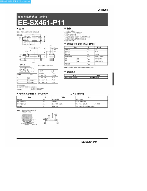
EE-SX461-P11
(2)
Panel
(1) (1)
按下安装孔,非常适合安装Photomicrosen-不良.当安装微型光电到已按 压安装孔的微型光电传感器面板,则一定要装入的微型光电传感器上 面板的按压侧,否则可能难以安装微型光电传感器和五至六千克的插入力可 以必需的.
■ 订购信息
描写 微型光电传感器(透射)
Model EE-SX461-P11
推荐配套连接器:
泰科电子AMP 171822-3(压接连接器)
172142-3(压接连接器)
OMRON
EE-1005(带安全带)
■ 电气和光学特性(Ta = 25°C,V
消耗电流 低电平输出电压 高电平输出电压 响应频率
Item
EE-1005 Connector
1,000±20
Light interrupting plate
ON
Distance d (mm)
−3
−2
−1
0
1
2
3
Distance d (mm)
(1) (2)
No. Name 1 容器
住房
2 容器
联系
3 铅丝
(3 )
Model
数量
171822-3
1
170262-1
Panel Mounting tab
微型光电传感器(透射)
EE-SX461-P11
芯片中文手册,看全文,戳
MEMO
微型光电传感器(透射)
EE-SX461-P11
OMRON EE-SX1108微型光电传感器 [透过型] 说明书
![OMRON EE-SX1108微型光电传感器 [透过型] 说明书](https://img.taocdn.com/s3/m/f9a871ea6294dd88d0d26b78.png)
CSM_EE-SX1108_DS_C_1_1EE-SX1108微型光电传感器[透过型]■电气及光学特性 (T a = 25°C)项目记号特性值单位条件MIN.TYP.MAX.发光侧正向电压V F —— 1.1 1.3V I F = 5mA 反向电流I R ————10μA V R = 5V 最大发光波长λ P ——940——nm I F = 20mA受光侧光电流I L 50150500μA I F = 5mA ,V CE = 5V 暗电流I D ————100nA V CE = 10V ,0 l x泄漏电流I LEAK——————μA —————集电极发射极之间的饱和电压V CE (sat)——0.10.4V I F = 20mA ,I L = 50μA最大光谱灵敏度波长λ P ——900——nm —————上升时间t r ——10——μs V CC = 5V ,R L = 1k ΩI L = 100μA下降时间t f——10——μsV CC = 5V ,R L = 1k ΩI L = 100μA■外形尺寸(单位:mm )■特征•实现传感器宽度 5mm 、凹槽宽度 2mm 的超小型传感器•印刷线路板表面实装型•高分辨率(狭片宽度 0.3mm )■绝对最大额定值 (T a = 25°C)项目记号额定值单位发光侧正向电流I F 25mA 正向脉冲电流I FP 100mA 反向电压V R 5V 受光侧集电极发射极之间的电压V CEO 20V 发射极集电极之间的电压V ECO 5V 集电极电流I C 20mA 集电极损耗P C 75mW 动作温度Topr -30~+85℃保存温度Tstg -40~+90℃焊接温度Tsol350(手工焊接)255(回流焊接)℃*1环境温度超过 25℃ 时,请参阅温度额定值图。
*2占空比 1%、脉冲宽度 0.1ms*3焊接时间为手工焊接 3 秒以内、回流焊接 10 秒以内*1*2*1*3EE-SX1108E E S X 1108-微型光电传感器■额定值·特性曲线图 2.正向电流—正向电压特性 (TYP .)图 3.光电流—正向电流特性 (TYP .)图 4.光电流—集电极发射极之间的电压特性 (TYP .)图 5.相对光电流—环境温度特性 (TYP .)图 6.暗电流—环境温度特性 (TYP .)图 7.应答时间—负载电阻特性 (TYP .)图 8.检测位置特性 (TYP .)图 9.检测位置特性 (TYP .)图 10.应答时间测定回路18●编带尺寸(单位:mm)●编带形式●数量2,000 个 / 卷EE-SX1108EE S X 1108-微型光电传感器■实际安装时须注意●回流焊接(1)建议使用以下规格的锡膏。
- 1、下载文档前请自行甄别文档内容的完整性,平台不提供额外的编辑、内容补充、找答案等附加服务。
- 2、"仅部分预览"的文档,不可在线预览部分如存在完整性等问题,可反馈申请退款(可完整预览的文档不适用该条件!)。
- 3、如文档侵犯您的权益,请联系客服反馈,我们会尽快为您处理(人工客服工作时间:9:00-18:30)。
Ultra-Compact Photomicrosensors with Surface-Mount Designs Surface mount design, and tape and reel packaging facilitate automated PCBassemblys Compact size makes these sensors ideal for use in applications with restrictedspaces High-resolution sensing withphototransistor outputs Dual channel model that is ideal for encoder applications (EE-SX1131) Ordering Information2EE-SX1107/1108/1109/1131 s ABSOLUTE MAXIMUM RATING (T A=25°C)Specificationss CHARACTERISTICS (T A=25°C)Note:Refer to Engineering Data if the ambient temperature is not within the normal room temperature range.Note:The following figures show the rising time (t r) and falling time (t f).utputtt90%10%t r t fInputOVI LR L3EE-SX1107/1108/1109/1131Engineering DataNote:The operating conditions of the photomicrosensor must be within the absolute maximum rating ranges.1401208040200-40-2020406080100C o l l e c t o r d i s s i p a t i o n P C (m W )Ambient temperature Ta (°C)10060504030200-40-20020406080100F o r w a r d c u r r e n t I F (m A )Ambient temperature Ta (°C)10F o r w a r d c u r r e n t I F (m A )Forward voltage V F (V)L i g h t c u r r e n t I L (µA )Forward current I F (mA)L i g h t c u r r e n t I L (µA )Forward current I F (mA)L i g h t c u r r e n t I L (µA )Collector-emitter voltage V CE (V)28101214L i g h t c u r r e n t I L (µA )Collector-emitter voltage V CE (V)46028101214L i g h t c u r r e n t I L (µA )Collector-emitter voltage V CE (V)46-40-2020406080100L l i g h t c u r r e n t I L (%)Ambient temperature Ta (°C)D a r k c u r r e n t I D (n A )Ambient temperature Ta (°C)R e s p o n s e t i m e t r , t f (µs )Load resistance R L (K Ω)s TEMPERATURE CHARACTERISTICSs INPUT CHARACTERISTICS (TYPICAL)s INPUT/OUTPUT CHARACTERISTICS (TYPICAL)EE-SX1107EE-SX1108/1131EE-SX1109L i g h t c u r r e n t I L (µA )Forward current I F (mA)s OUTPUT CHARACTERISTICS (TYPICAL)EE-SX1107EE-SX1108/1131EE-SX1109s LIGHT CURRENT TEMPERATUREDEPENDENCY (TYPICAL)s DARK CURRENT TEMPERATUREDEPENDENCY(TYPICAL)s RESPONSE TIME CHARACTERISTICS (TYPICAL)4EE-SX1107/1108/1109/1131RelativelightcurrentIL(%)Distance: d (mm)120100604020RelativelightcurrentIL(%)Distance: d (mm)80RelativelightcurrentIL(%)Distance: d (mm)RelativelightcurrentIL(%)Distance: d (mm)120100604020RelativelightcurrentIL(%)Distance: d (mm)80RelativelightcurrentIL(%)Distance: d (mm) DimensionsUnit: mm (inch)s EE-SX1107Note: 1. Unless otherwise specified, tolerances are ±0.15 mm.2. The values in brackets are relative dimensions.EE-SX1107s SENSING POSITION CHARACTERISTICS (TYPICAL)EE-SX1108/1109/1131s SENSING POSITION CHARACTERISTICS (TYPICAL)EE-SX1108EE-SX1109EE-SX1131(Cross section AA view)5EE-SX1107/1108/1109/1131s EE-SX1108Note: 1. Unless otherwise specified, tolerances are ±0.15 mm.2. The values in brackets are relative dimensions.Pin assignmentRecommended soldering patternAnode Cathode Collector EmitterEC KAPin assignmentAnode Cathode Collector EmitterEC K ARecommended soldering pattern(Cross section AA view)6EE-SX1107/1108/1109/1131Unit: mm (inch)s EE-SX1109Pin assignmentAnodeCathodeCollectorEmitterECKARecommended soldering pattern(Cross section AA view)Note: 1. Unless otherwise specified, tolerances are ±0.15 mm.2. The values in brackets are relative dimensions.7EE-SX1107/1108/1109/1131s EE-SX1131Note: 1. Unless otherwise specified, tolerances are ±0.15 mm.2. The values in brackets are relative dimensions.Pin assignmentRecommended soldering patternNC AC E1E2Collector Emitter 1Emitter 2K(Cross section AA view)8EE-SX1107/1108/1109/1131s TAPE AND REELReelUnit: mm (inch)Tape configurationPart numberPieces per reelEE-SX11072500EE-SX1108/EE-SX11312000EE-SX11091000Quantity per reelPart number h l m nEE-SX1109 5.2 (0.20) 6.2 (0.24)0.25 (0.01) 4.2 (0.17)Part number h l m nEE-SX1107 3.2 (0.13) 3.6 (0.14)0.9 (0.04) 3.2 (0.13)EE-SX1108 4.2 (0.17) 5.2 (0.20)0.25 (0.01) 4.2 (0.17)EE-SX1131 4.2 (0.17) 5.2 (0.20)0.25 (0.01) 4.2 (0.17)9EE-SX1107/1108/1109/1131Manual soldering•"Sn 60" (60% tin and 40% lead) or solder with silver content is recommended.•Use a soldering iron of less than 25W. The temperature of the iron tip must be kept above 300°C (572°F).•Solder each land for a maximum of 3 seconds.Precautionss SOLDERING INFORMATIONReflow soldering•Reflow soldering must be done within 48 hours after opening the aluminum envelope. The component must be stored under 30°C at 80% RH.•The following soldering paste is recommended:Melting temperature: 178~192°C Composition: Sn 63%, Pb 37%•Recommended thickness of metal mask is between 0.2 mm and 0.25 mm for screen printing.•The following chart illustrates the maximum temperature limits for soldering:T e m p e r a t u r e (°C )TimeOMRON ELECTRONICS LLCOMRON CANADA, INC.One East Commerce Drive 885 Milner AvenueSchaumburg, IL 60173Scarborough, Ontario M1B 5V81-800-55-OMRON416-286-6465Cat. No. E02DAD23/01Specifications subject to change without notice.Printed in the U.S.A.。