2SD1816-T-TM3-B-R中文资料(Unisonic Technologies)中文数据手册「EasyDatasheet - 矽搜」
新蒂尔电子有限公司产品说明书
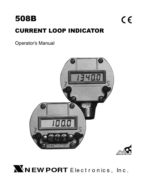
508BCURRENT LOOP INDICATOR Operator’s ManualNEWPORT Electronics, Inc.®CountersFrequency Meters PID Controllers Clock/Timers Printers Process Meters On/Off ControllersRecorders Relative Humidity Transmitters Thermocouples ThermistorsWireRate Meters Timers TotalizersStrain Gauge MetersVoltmeters MultimetersSoldering Iron TesterspH pens pH Controllers pH ElectrodesRTDs Thermowells Flow SensorsNEWPORT Electronics, Inc.®For Immediate AssistanceIn the U.S.A. and Canada: 1-800-NEWPORT®In Mexico: (95) 800-NEWPORT SMOr call your local NEWPORT Office.Internet e-mail ******************Additional products fromNEWPORTnet SMOn-Line ServiceIt is the policy of NEWPORT to comply with all worldwide safety and EMC/EMI regulations that apply.NEWPORT is constantly pursuing certification of its products to the European New Approach Directives. NEWPORT will add the CE mark to every appropriate device upon certification.The information contained in this document is believed to be correct but NEWPORT Electronics, Inc.accepts no liability for any errors it contains, and reserves the right to alter specifications without notice.WARNING:These products are not designed for use in, and should not be used for, patient connected applications.This device is marked with the international caution symbol. It is important to read the Setup Guide before installing or commissioning this device as it contains important information relating to safety and EMC.TABLE OF CONTENTS1.0DESCRIPTION . . . . . . . . . . . . . . . . . . . . . . . . . . . . . . . . . . . . . . . . . . . . . . . . . . . . . . . .11.1Definition/Application . . . . . . . . . . . . . . . . . . . . . . . . . . . . . . . . . . . . . . . . . . . . . .11.2Features . . . . . . . . . . . . . . . . . . . . . . . . . . . . . . . . . . . . . . . . . . . . . . . . . . . . . . . .12.0SPECIFICATIONS . . . . . . . . . . . . . . . . . . . . . . . . . . . . . . . . . . . . . . . . . . . . . . . . . . . . .22.1Input . . . . . . . . . . . . . . . . . . . . . . . . . . . . . . . . . . . . . . . . . . . . . . . . . . . . . . . . . . .22.2Accuracy . . . . . . . . . . . . . . . . . . . . . . . . . . . . . . . . . . . . . . . . . . . . . . . . . . . . . . . .32.3Display . . . . . . . . . . . . . . . . . . . . . . . . . . . . . . . . . . . . . . . . . . . . . . . . . . . . . . . . .32.4Conversion . . . . . . . . . . . . . . . . . . . . . . . . . . . . . . . . . . . . . . . . . . . . . . . . . . . . . .32.5Environmental . . . . . . . . . . . . . . . . . . . . . . . . . . . . . . . . . . . . . . . . . . . . . . . . . . . .32.6Mechanical . . . . . . . . . . . . . . . . . . . . . . . . . . . . . . . . . . . . . . . . . . . . . . . . . . . . . .43.0MECHANICAL ASSEMBLY AND INSTALLATION . . . . . . . . . . . . . . . . . . . . . . . . . . . . . .43.1Safety Considerations . . . . . . . . . . . . . . . . . . . . . . . . . . . . . . . . . . . . . . . . . . . . . .43.2Intrinsic Safety Parameters for FM(FACTORY MUTUAL) . . . . . . . . . . . . . . . . . .43.4Mechanical Installation . . . . . . . . . . . . . . . . . . . . . . . . . . . . . . . . . . . . . . . . . . . . .53.5Standard Mounting . . . . . . . . . . . . . . . . . . . . . . . . . . . . . . . . . . . . . . . . . . . . . . . .64.0SIGNAL INPUT CONNECTIONS . . . . . . . . . . . . . . . . . . . . . . . . . . . . . . . . . . . . . . . . .104.1508B-1 . . . . . . . . . . . . . . . . . . . . . . . . . . . . . . . . . . . . . . . . . . . . . . . . . . . . . . . .104.2508B-2 and 508B-3 . . . . . . . . . . . . . . . . . . . . . . . . . . . . . . . . . . . . . . . . . . . . . . .105.0CONFIGURATION AND CALIBRATION . . . . . . . . . . . . . . . . . . . . . . . . . . . . . . . . . . . .115.1Glossary . . . . . . . . . . . . . . . . . . . . . . . . . . . . . . . . . . . . . . . . . . . . . . . . . . . . . . .115.2Calculation . . . . . . . . . . . . . . . . . . . . . . . . . . . . . . . . . . . . . . . . . . . . . . . . . . . . .125.3Alternate FS Calculation . . . . . . . . . . . . . . . . . . . . . . . . . . . . . . . . . . . . . . . . . . .135.4FS Procedure Implementation . . . . . . . . . . . . . . . . . . . . . . . . . . . . . . . . . . . . . .135.5Component Access/Unit Calibration . . . . . . . . . . . . . . . . . . . . . . . . . . . . . . . . . .145.6Labels . . . . . . . . . . . . . . . . . . . . . . . . . . . . . . . . . . . . . . . . . . . . . . . . . . . . . . . . .166.0 INTRINSIC SAFETY CONSIDERATIONS . . . . . . . . . . . . . . . . . . . . . . . . . . . . . . . . . . . . .18FiguresPage Figure 1-1 Model 508B . . . . . . . . . . . . . . . . . . . . . . . . . . . . . . . . . . . . . . . . . . . . . . . . . .1 Figure 3-1 Basic Mounting Configurations . . . . . . . . . . . . . . . . . . . . . . . . . . . . . . . . . . . .5 Figure 3-2 Surface and TR2/2TK Relay Track Mounting (Option MAT1) . . . . . . . . . . . . .7 Figure 3-3 DIN Track Mounting (Option MDT1) . . . . . . . . . . . . . . . . . . . . . . . . . . . . . . . .7 Figure 3-4. External Explosion-Proof Housing Mounting (Option MXS1) . . . . . . . . . . . .8 Figure 3-5. External Explosion-Proof Housing Mounting (Option MXS2) . . . . . . . . . . . .9 Figure 3-6. External Explosion-Proof Housing Mounting (Option EPW2) . . . . . . . . . . . .9 Figure 4-1 508B-1 Signal Connections . . . . . . . . . . . . . . . . . . . . . . . . . . . . . . . . . . . . .10 Figure 4-2 508B-2 & 508B-3 Signal Connections . . . . . . . . . . . . . . . . . . . . . . . . . . . . .10 Figure 5-1. 508B-2 and 508B-3 Case Access . . . . . . . . . . . . . . . . . . . . . . . . . . . . . . . .14 Figure 5-2. Calibration Setup . . . . . . . . . . . . . . . . . . . . . . . . . . . . . . . . . . . . . . . . . . . . .15 Figure 5-3. Label Placement . . . . . . . . . . . . . . . . . . . . . . . . . . . . . . . . . . . . . . . . . . . . .16 Figure 5-4. Jumper Locations . . . . . . . . . . . . . . . . . . . . . . . . . . . . . . . . . . . . . . . . . . . .17 Figure 6-1 Block Diagram for 508B Usage for Factory Mutual . . . . . . . . . . . . . . . . . . .19TablesTable 5-1. Configuration Chart . . . . . . . . . . . . . . . . . . . . . . . . . . . . . . . . . . . . . . . . . . . .171.0DESCRIPTIONFigure 1-1. Model 508B1.1DEFINITION/APPLICATIONModel 508B is a signal powered, two-wire current-loop indicator that accepts 1-5 mA,4–20mA, or 10-50 mA process signals and digitally display (±2000 active counts) the process variable in either percent or in engineering units for such parameters as pressure, flow,temperature, and level.1.2FEATURESIn-field ProgrammabilityInput ranges (1-5 mA, 4-20 mA, or 10-50 mA) are selected by push-on jumpers. Three decimal points and a dummy right-hand zero may also be selected by push-on jumpers. Zero and span may be fine tuned with precision, 25-turn potentiometers. Positive slope response may be changed to negative slope response (e.g. , +6000 to –18000) by simply changing two other push-on jumpers.(.078)Signal PoweredModel 508B obtains operating power directly from the current loop, requiring a drop of lessthan 2.5 V or 2.5 mW at 1 mA.Electrical Isolation/Overrange ProtectionThe 508B is electrically isolated from its case and is immune to most sources of electricalnoise encountered in process-control environments. In the event of input overrange currents, the 508B can tolerate 250 mA in the forward direction and 1000 mA reverse.Vibration/Shock/Water ResistanceLow mass and multi-point circuit board support give excellent vibration and shock resistance.Sturdy, die-cast construction, polyurethane paint,and full fluorosilicone gasketing ensure avirtually waterproof case.Circuit boards are conformally coated for added humidity protection.Mounting VersatilityThe 508B-1 may be mounted in a control room on either American or European relay tracks with snaptrack adaptors. The unit can be wall mounted using an available bulkhead adaptor or mounted in an explosion-proof enclosure for wiring compatibility with other equipment in hazardous environments.Both the 508B-2 and the 508B-3 may be connected directly to a conduit with a "T" junction box.2.0SPECIFICATIONS2.1INPUTCurrent:1-5 mA, 4-20 mA, or 10-50 mA(jumper selectable)Voltage drop: 2.5 V max forward; up to 50 mAProtection:250 mA forward at 3 V or 6 V with IS option;1000 mA reverse at 2.5 VZero range:–2510 to +2000 counts; jumper selectable in 4 overlappingcoarse ranges with a 25-turn potentiometer for continuousadjustment within the following selected ranges: –2510 to–1420; –1580 to –420; –470 to +850; and +760 to +2000.Span range:0 to 2000 counts, continuously adjustable with 25-turnpotentiometerNormal mode rejection:46 dB min at 50/60 HzCommon mode rejection:120 db typical, dc to 60 HzCommon mode voltage:700 V peak from dc to 60 Hz (meter to case)RFI susceptibility:Less than ±0.5% of span at a distance of one meter from a2-watt, hand-held transceiver (approximately equivalent to10 V/m field strength) at frequencies of 27 MHz or 440 MHzNOTE: Proper lead dress and shielding required.2.2ACCURACYAccuracy:Within ±0.1% Span ±1 Count at +25°CZero Tempco:±0.1 Count/K typ. , ±0.2 Count/K max.Span Tempco:±0.005% Span/K typ. , ±0.015% Span/K max.2.3DISPLAYType:7-segment LCD, 8.9 mm (0.350 in) highColor:Black digits on white backgroundSymbols:–1.8.8.80Polarity:Minus signOverrange:Three least significant digits blankedExtra digit:Dummy right-hand zero is jumper selectableDecimal points:Three positions, jumper selectableLifetime:More than 30,000 hours to 2:1 contrast ratioTemperature derating:2:1 lifetime reduction for each 10°C above 60°CHumidity derating:2:1 lifetime reduction for each 10%RH above 60%RH2.4CONVERSIONTechnique:Dual-slope, average-value with autozero correctionPolarity:Determined automatically at the end of signal integrationperiodSignal integration period:100 mS typ.Reading rate: 2.5/sec2.5ENVIRONMENTALTemperature:-40 TO +85°CHumidity:To 95% at 40°CVibration: 1.52 mm (.06 in) double amplitude, 10-80 Hz cycledShock55 g, half-sine, 9-13 msec durationWater resistance Watertight to a proof pressure of 35 kPa (5 psi)Mounting position:Any2.6MECHANICALWeight:400 g (14 oz)Diameter:74 mm (2.9 in)Height:48 mm (1.9 in) including barrierElectrical connections:Standard: 3-position barrier strip with #6 screw wire clampsOptional: Two #18 stranded wires, 305 mm (12 in) long3.0MECHANICAL ASSEMBLY AND INSTALLATION3.1SAFETY CONSIDERATIONSTo ensure safe operation follow the guidelines below:VISUAL INSPECTION: Do not attempt to operate the instrument if damage is found.This instrument will meet the requirements of certain FM safety certifications for hazardousenvironments. In order to meet these requirements the appropriate intrinsic safety barrier must be included in the installation to limit the voltage and current that may be introduced in thehazardous environment.EXERCISE CAUTION: Due to certain current loop installations, high common mode voltages may be present on the loop circuits. Become familiar with the possible hazards that your circuit may present before installing this meter or, to be safe, remove all sources of power to thecircuit while installing.RAIN OR MOISTURE: Do not expose the instrument to condensing moisture.3.2INTRINSIC SAFETY PARAMETERS FOR FM(FACTORY MUTUAL)Certificate No. 5X2A0.AXV max=12.5 V,I max=250 mAIntrinsically Safe for Class I, II and III, Division 1, Groups A,B,C,D,E,F and G hazardouslocations.Ci=8.6 µFLi=0 mH3.3MECHANICAL INSTALLATIONRear view: Standard, integral mounting plate508B-1508B-2 and 508B-3Figure 3-1 Basic Mounting Configurations12.7 mm or 1/2 inch conduitThe 508B is packaged in a small, rugged, die-cast, zinc-alloy case designed to fit 3" I.D.or larger housings, requiring less than 2" of height.Three basic 508B configurations (508B-1, 508B-2, and 508B-3) provide mounting versatility.The 508B-1 provides for surface, track, or explosion-proof housing mounting and isconnected with a 3-terminal, #6 screw barrier strip (beneath the display window).The 508B-2 is equipped with a 1/2" EMT conduit fitting on the case side beneath the display.The fitting has two 0.3 millimeter long, #18 stranded insulated wires passing through aneoprene moisture plug for hookup to junction boxes with standard wire nuts.The 508B-3 is equipped with a 1/2" NPT conduit fitting on the case side beneath the display.The fitting has two 0.3 mm long, #18 stranded insulated wires passing through a neoprene moisture plug for hookup to junction boxes with standard wire nuts.3.4STANDARD MOUNTINGTapped holes on the back of the 508B case provide for custom mounting to a flat surface;integral flanges on the back of the case provide for standard 8TK2 relay track mounting.For flat surface mounting, use #6 hardware.For 8TK2 relay track mounting, simply push onto track.The following optional adaptors provide additional mounting options:1.Adapter plate for surface mount with two #8 front-entry screws through keyhole slots or forpush-mount into TR2/2TK relay track. (Option MAT1)2.Rail clamp for push mount onto DIN EN 50 022 relay track. (Option MDT1)3.Spring retainers for mounting in 76.4 to 88.9 mm (3 to 3.5 in) inside diameter explosion-proof housings.(Option MXS1)4.Wire brackets for mounting the 508B above a transmitter in a single housing.(Option MXS2)ADAPTER MOUNTINGRELAY TRACK MOUNTING (FOR TR2/2TK TRACK R.D.I.)Figure 3-2 Surface and TR2/2TK Relay Track Mounting (Option MAT1)1.Position plate for desired application.2.Use #6 hardware to mount plate to the back of the case.Figure 3-3 DIN Track Mounting (Option MDT1)1.Position plate for desired track direction.e #6 flathead screws to mount plate to the back of the case.3.Snap case assembly onto DIN rail.CASESCREW (4 REQ’D)CASEADAPTER PLATESCREW (4 REQ’D)CASEADAPTER PLATESCREW (4 REQ’D)CASESCREW (4 REQ’D)DIN RAIL LATCHDIN RAIL ADAPTERDIN RAIL ADAPTERDIN RAIL LATCHDIN TRACK(DIN EN 50 022)DIN TRACK (DIN EN 50 022)TOP VIEW OF EXPLOSION-PROOF HOUSING.UNIT AND HOUSING SHOWN FOR REFERENCE ONLY .Spring Retainer for Explosion-Proof HousingFigure 3-4. External Explosion-Proof Housing Mounting (Option MXS1)1.Position spring retainers across the back of the case.e wire protector feet (4 provided with Option MXS1) to hold spring retainers in place.3.Press case assembly into explosion-proof housing.CASESCREW (4 REQ’D)1/2” N.P .T.BOTH ENDSBRACKET (2 REQ’D)8 MM HEX (5/16)Figure 3-5. External Explosion-Proof Housing Mounting (Option MXS2)1.Install brackets using #6 screws and flat washers.2.Mount 508B above transmitter as shown in Figure 3-6.3.Press wires to pass into housing.Figure 3-6. External Explosion-Proof Housing Mounting (Option EPW2)CASESCREW (4 REQ’D)WASHERS (4 REQ’D)WIRE BRACKETS (2 REQ’D)508BWIRE BRACKETSTRANSMITTER4.0SIGNAL INPUT CONNECTIONSWARNING: Input currents in excess of protective limits can damage your meter4.1508B-1The 508B-1 has a 3-terminal barrier strip on the front of the case below the display window.The signal inputs are marked with a "+" or a "–" symbol. The third terminal (case ground) is marked with a "/ / / " e of a shielded cable, properly dressed, is recommended.4.2508B-2 and 508B-3Both the 508B-2 and 508B-3 come equipped with a male conduit fitting on the side of the case.The 508B-2 fitting is 1/2" EMT; the 508B-3 fitting is 1/2" NPT. Each conduit fitting is plugged with a rubber stopper. Two 0.3 millimeter long, #18 stranded insulated wires are passed through each stopper.The two wires are white and black. The black wire is the "+"signal input; the white wire is the "–" signal input. Either unit can be hooked up using standard wire nuts.Figure 4-1 508B-1 Signal ConnectionsScrew-Terminal Pin Assignment 1+ SIGNAL INPUT 2– SIGNAL INPUT 3GROUNDFigure 4-2 508B-2 & 508B-3 SignalConnections Terminal Wire Assignment BLACK WIRE + SIGNAL INPUT WHITE WIRE – SIGNAL INPUT5.0CONFIGURATION AND CALIBRATIONThe factory setup (FS) option procedure is to configure the 508B for a specific application.Customers may specify any two current inputs and their corresponding digital readings.For optional configuration procedures, see Section5.3.The unit may be configured using the push-on jumpers already positioned on the pin-forest.Pin-forest designations are illustrated in Figure5-4.5.1GLOSSARYThe following terms and their definitions appear throughout the following procedures: DP1 Decimal point 1.999DP2 Decimal point 19.99DP3 Decimal point 199.9DRHZ Dummy right-hand zeroG Gain expressed in counts per mAI1 Lowest input current in mAI2 Highest input current in mAN1 Reading in displayed counts at input current I1N2 Reading in displayed counts at input current I2RN Required range number for zero range selectionRSS Reverse span slopeZR1 Zero range (-2510 to -1420)ZR2 Zero range (-1580 to -420)ZR3 Zero range (-470 to +850)ZR4 Zero range (+760 to +2000)5.2CALCULATIONNOTE: An alternate FS calculation procedure is given in Section 5.31.Base all calculations on one of three ranges: 1 mA to 5 mA, 4 mA to 20 mA, or 10 mA to50 mA. Write results of calculations in blanks provided below each procedural step.2.Determine the lowest input current, I1, specified by the customer:I1 = _________mA3.Determine the highest input current, I2, specified by the customer:I2 = _________mA4.Determine the reading, N1, at input current, I1, specified by the customer:N1 = _________counts5.Determine the reading, N2, at input current, I2, specified by the customer:N2 = _________counts6.Calculate the gain (G1):G = (N2 - N1) =( - ) counts per mA(I2 -I1) ( - )7.Calculate the required range number:RN = N1 - (I1 x G) =_________NOTE: If G is greater than 500, it is out of the operating range for the standard unit.8.Select the zero range, ZR, that includes the required range number, RN, from thefollowing ranges:ZR1 = -2510 to -1420ZR2 = -1580 to -420ZR3 = -470 to +850ZR4 = +760 to +20009. Proceed to FS Procedure Implementation, Section 5.4.5.3ALTERNATE FS CALCULATION1. (Line 1) Low signal input (mA) =_______________________2. (Line 2) High signal input (mA) =_______________________3. (Line 3) Low signal input reading (counts)_______________________4. (Line 4) High signal input reading (counts) =_______________________5. (Line 5) Line 2 - Line 1 =_______________________6. (Line 6) Line 4 - Line 3 =_______________________7. (Line 7) Line 6 divided by Line 5 =_______________________8. (Line 8) Line 7 x Line 1 =_______________________9. (Line 9) Line 3 - Line 8 =_______________________10.Select a zero range from one of the following,where the number on Line 9 falls between thehigh and low numbers of that ZR range:ZR1 = -2510 to -1420ZR2 = -1580 to -420ZR3 = -470 to +850ZR4 = +760 to +200011.Proceed to FS Procedure Implementation, Section 5.4.5.4FS PROCEDURE IMPLEMENTATIONPin-forest designations are illustrated in Figure 5-4Jumper Locations. Range and displayselection are listed in Table 5-1Configuration Chart.1.If the current range chosen in either Section 5.2Step 1 or Section5.3Steps 1 and 2equals either 4 mA to 20 mA or 10 mA to 50 mA, install a push-on jumper as indicated inTable5-1.2. If N1 (5.2Step 3 or 5.3Step 3) is more positive than N2 (5.2Step 5 or 5.3Step 4),reverse the span slope (RSS) by installing two push-on jumpers as indicated inTable5-1.3. Select the zero range required (ZR1, ZR2, ZR3, or ZR4), and install a push-on jumper asindicated in Table5-1.4. If a dummy right-hand zero (DRHZ) is required, install a push-on jumper as indicated inTable5-1.5. If a decimal point is required (DP1, DP2, DP3), install a push-on jumper as indicated inTable5-1.5.5COMPONENT ACCESS/UNIT CALIBRATIONTools and Equipment#2 Phillips screwdriverJewelers' slotted screwdriverPrecision milliampere power sourceor10 V power supply, 4 1/2 digit DMM with milliampere range and 10 kOhm rheostatFigure 5-1. 508B-2 and 508B-3 Case Access420100.000.0mA=mA=INPUTCURRENTDISPLAYREADINGFigure 5-2. Calibration Setup1.Remove 4 Phillips-head screws from the top of the 508B case, and lift main unit fromcase. (See Figure 5-1)2.Select the desired jumper configuration and install push-on jumpers in locations indicatedin the Table 5-1Configuration Chart. (See Figure 5-4)3.Pull off two sealing plugs that cover 508B span and zero potentiometer screw heads.4.Set up 508B in calibration configuration. (See Figure 5-2)NOTE:Store unused jumpers in a vertical position on unused upper pins closest to thedisplay board.5.Calibrate unit as follows:A.Alternately apply input currents I1 and I2, and adjust span pot (S) until span reading equals N 2- N 1counts.B.Apply input current, I1, and adjust the zero pot (Z) until a reading equal to N1 is displayed.6.Remove 508B from calibration setup.7.Replace two sealing plugs over 508B span and zero potentiometer screw heads.8. Apply labels as described in Section 5.6. (See Figure 5-3).9.Replace 508B main unit in case.10. Replace 4 Phillips-head screws that hold the 508B unit to the case.5.6LABELSFigure 5-3. Label Placement1. Add new label directly over existing label. Add correct values of I1, I2, N1, and N2.2. Install one label on the outside of the housing as shown above.3. Install one label on the wire shield as shown above.420100.000.0mA =mA =INPUT CURRENT DISPLAYREADINGFigure 5-4. Jumper LocationsTable 5-1. Configuration ChartConfiguration Push-On Jumpers1-5 mA NONE4-20 mA J*10-50 mA ANormal span slope G,a*Reverse span slope F,ZZero range -2510 to -1420 (ZR1) IZero range -1580 to -420 (ZR2) TZero range -470 to +850 (ZR3) NONEZero range +760 to +2000 (ZR4) cDummy right-hand zero (DRHZ) DDecimal Point 1.999 (DP1) WDecimal Point 19.99 (DP2) VDecimal Point 199.9 (DP3) L** Default SettingNOTE: The factory-calibrated configuration shows 00.0 to 100.0 for a 4 to 20 mA input.6.0 INTRINSIC SAFETY CONSIDERATIONSFigure 6-1 Block Diagram for 508B Usage for Factory MutualNOTES:1.Apparatus which is unspecified except that it must not be supplied from nor containunder normal or abnormal conditions a source of potential with respect to Earth inexcess of 250V R.M.S. or250V D.C.2.The following output parameters apply; Vmax=12.5V, Imax=250mA, Ci=6.2uF,Li=0.3.The Interconnecting Cable may be a twin pair, or a pair contained in a Type A orType B multicore cable (as defined in EN50 039 clause 5.3) provided that the peakvoltage of any circuit contained within the multicore does not exceed 60 Volts.4.The capacitance or inductance or inductance to resistance (4R) ratio of theInterconnecting Cable must not exceed the values specified for the barrier in use.5The electrical circuit in the Hazardous Area must be capable of withstanding without breakdown an A.C. test voltage of 500V R.M.S. to Earth or frame for oneminute.For immediate technical or application assistance please call:Newport Electronics, Inc.2229 South Yale Street • Santa Ana, CA • 92704 • U.S.A.TEL: (714) 540-4914 • FAX: (203) 968-7311TollFree:1-800-639-7678••e-mail:******************ISO 9001 CertifiedNewport Technologies, Inc.976 Bergar • Laval (Quebec) • H7L 5A1 • CanadaTEL: (514) 335-3183 • FAX: (514) 856-6886TollFree:1-800-639-7678•www.newport.ca•e-mail:***************Newport Electronics, Ltd.One Omega Drive • River Bend Technology CentreNorthbank, Irlam • Manchester M44 5BD • United KingdomTel: +44 161 777 6611 • FAX: +44 161 777 6622TollFree:0800488488••e-mail:******************.ukNewport Electronics B.V.Postbus 8034 • 1180 LA Amstelveen • The NetherlandsTEL: +31 20 3472121 • FAX: +31 20 6434643TollFree:08000993344•www.newport.nl•e-mail:***************Newport Electronics spol s.r.o.Frystatska 184, 733 01 Karviná • Czech RepublicTEL: +420 59 6311899 • FAX: +420 59 6311114TollFree:0800-1-66342•www.newport.cz•e-mail:***************Newport Electronics GmbHDaimlerstrasse 26 • D-75392 Deckenpfronn • GermanyTEL: 49 7056 9398-0 • FAX: 49 7056 9398-29TollFree:0800/6397678•www.newport.de•e-mail:****************Newport Electronique S.A.R.L.11, rue Jacques Cartier • 78280 Guyancourt • FranceTEL: +33 1 61 37 29 00 • FAX: +33 1 30 57 54 27TollFree:0800466342•www.newport.fr•e-mail:****************Mexico and Latin AmericaFAX: 001 (203) 359-7807En Español: 001 (203) 359-7803。
2SC3356超高频低噪声NPN晶体管说明书
描述2SC3356是超高频低噪声晶体管,采用平面NPN 硅外延双极型工艺。
具有高功率增益、、低噪声系数、、大动态范围和理想的电流特性,采用SOT-23贴片式封装,主要应用于VHF ,UHF 和CATV 高频宽带低噪声放大器。
主要特性高增益:︱S 21e ︱2典型值为12dB @V CE =10V ,I C =20mA ,f=1GHz 低噪声:NF 典型值为1.5dB @V CE =10V ,I C =7mA ,f=1GHz 增益带宽乘积:f T 典型值为7GHz@V CE =10V ,I C =20mA ,f=1GHz极限工作条件范围(TA=25℃)参数符号极值单位集电极基极击穿电压VCBO 20V 集电极发射极击穿电压VCEO 12V 发射极基极击穿电压VEBO 3V 集电极电流IC 100mA 功耗PC 200mW 结温度Tj150℃存储温度Tstg-65~+150℃HFE 档位分档BC D标号R25HFE80-140120-180170-260高频低噪声晶体管NPN电学特性(TA=25℃)参数符号最小典型最大单位测试条件集电极基极击穿电压VCBO20V IC=1.0µA集电极基极漏电流ICBO0.1µA VCB=10V发射极基极漏电流IEBO0.1µA VEB=1V增益带宽乘积f T 5.57GHz VCE=10V,IC=20mA输出反馈电容Cre0.65pF VCB=10V,IE=0mA,f=1MHz 功率增益|S21e|212dB VCE=10V,IC=20mA,f=1GHz 噪声因子NF 1.5dB VCE=10V,IC=7mA,f=1GHz封装形式SOT-23管脚定义:1:基极(Base)2:发射极(Emitter)3:集电极(Collector)典型特性曲线(TA=25ºC)SMITH图测试条件:V CE=10V,I C=20mAS21e-FREQUENCY S12e-FREQUENCYS11e-FREQUENCY S22e-FREQUENCY散射参数(S-PARAMETER)测试条件:V CE=10V,I C=20mA,Z O=50Ω测试频率S11S21S12S22GHz MAG ANG MAG ANG MAG ANG MAG ANG0.1-4.4887-107.4227.586107.71-36.7649.128-2.9397-62.4680.2-6.7891-140.9824.2103.81-31.851.684-6.0189-57.3420.3-7.2322-163.1121.33898.039-28.86857.605-7.9522-56.7090.4-7.1858-176.0119.39292.782-26.98564.917-8.6659-57.3730.5-7.4501172.1117.74790.058-25.55767.75-8.9477-59.8750.6-7.3244160.4616.186.005-24.17368.77-9.3303-64.1410.7-7.2467153.4215.17483.595-22.9670.383-9.3035-68.4720.8-7.5163144.7114.09979.671-22.0275.134-9.169-72.8080.9-7.3334135.3312.76775.789-20.83875.774-9.3152-77.4451-7.2486129.312.44575.699-20.22175.086-9.2763-82.4171.1-7.6324120.8711.33768.982-19.77383.079-9.0412-89.481.2-7.5426112.2210.24867.1-18.2580.563-9.0646-93.1931.3-7.4681106.239.806568.457-17.79583.598-9.1476-98.6541.4-7.761599.0369.06960.986-17.35287.012-9.0139-105.221.5-7.713193.0697.813959.825-15.39486.83-8.4818-107.71.6-7.41884.7147.421764.124-15.54584.385-8.6765-112.921.7-7.749179.217.027155.497-14.62588.168-8.7946-120.511.8-7.552373.983 5.706757.787-13.12286.822-7.5139-125.481.9-6.42762.268 5.471959.598-13.18579.194-8.4837-131.52-6.862654.527 5.273953.898-12.21682.641-9.2253-140.882.1-7.020544.4053.802159.296-11.66976.371-7.9545-145.67。
TM1816_V1.0
OE
LE Rext=未接, OUT0~
OUT15=OFF Rext=1860Ω, OUT0~
OUT15=OFF Rext=744Ω, OUT0~
OUT15=OFF Rext=1860Ω, OUT0~
OUT15=ON Rext=744Ω, OUT0~
OUT15=ON
----3
--------0.8VD D GND
90
ns
十四、动态特性(VDD=3.3V)
特性 延迟时间
代表符
CLK-OUT tpLH1
LE-OUT tpLH2
测量条件
VDD=3.3V
最小值 一般值 最大值 单位
----
80
----
80
100
ns
100
ns
©Titan Micro Electronics
深圳市天微电子有限公司 王生 15818572651 QQ 3103278211
深圳市天微电子有限公司 王生 15818572651 QQ 3103278211
一、 特性描述
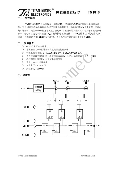
16 位恒流驱动 IC TM1816
TM1816是LED显示面板设计的驱动IC,它内建的CMOS位移寄存器与锁存功
能,可以将串行的输入数据转换成平行输出数据格式。TM1816具有16个电流源,可以在 每个输出端口提供3~45mA恒定电流量以驱动LED;且当环境发生变化时,对其输出电流影响 很小。同时可以选用不同阻值(REXT)的外接电阻来调整TM1816各输出端口的电流大小, 因此,可精确地控制 LED的发光亮度。也可以在每个输出端口串接多个LED。
三、结构图
©Titan Micro Electronics
深圳市天微电子有限公司 王生 15818572651 QQ 3103278211
2SK241中文资料
Maximum Ratings (Ta = 25°C)
Characteristics Drain-source voltage Gate-source voltage Drain current Drain power dissipation Channel temperature Storage temperature range Symbol VDS VGS ID PD Tch Tstg Rating 20 ±5 30 200 125 −55~125 Unit V V mA mW °C °C
Figure 1
Gps, NF Test Circuit
2
2003-03-27
2SK241
3
2003-03-27
2SK241
4
2003-03-27
2SK241
5
2003-03-27
2SK241
6
2003-03-27
2SK241
RESTRICTIONS ON PRODUCT USE
000707EAA
2SK241
TOSHIBA Field Effect Transistor Silicon N Channel MOS Type
2SK241
FM Tuner, VHF and RF Amplifier Applications
• • • • Low reverse transfer capacitance: Crss = 0.035 pF (typ.) Low noise figure: NF = 1.7dB (typ.) High power gain: GPS = 28dB (typ.) Recommend operation voltage: 5~15 V Unit: mm
2SD882L-D-TM3-B中文资料

UNISONIC TECHNOLOGIES CO., LTD2SD882NPN SILICON TRANSISTORMEDIUM POWER LOWVOLTAGE TRANSISTORFEATURES* High current output up to 3A * Low saturation voltage * Complement to 2SB772APPLICATIONS* Audio power amplifier * DC-DC convertor * Voltage regulator*Pb-free plating product number: 2SD882LORDERING INFORMATIONOrder NumberPin AssignmentNormal Lead Free Plating Package 1 2 3 Packing2SD882-x-T60-K 2SD882L-x-T60-K TO-126 E C B Bulk 2SD882-x-T6C-K 2SD882L-x-T6C-K TO-126C E C B Bulk 2SD882-x-TM3-T 2SD882L-x-TM3-T TO-251 B C E Tube 2SD882-x-TN3-R 2SD882L-x-TN3-R TO-252 B C E Tape Reel 2SD882-x-TN3-T 2SD882L-x-TN3-T TO-252 B C E Tube 2SD882-x-T9N-B 2SD882L-x-T9N-B TO-92NL E C B Tape Box 2SD882-x-T9N-K 2SD882L-x-T9N-K TO-92NL E C B BulkABSOLUTE MAXIMUM RATING (Ta=25 , unless otherwise specified )PARAMETER SYMBOL RATINGSUNITCollector-Base Voltage V CBO 40 VCollector-Emitter Voltage V CEO 30 VEmitter-Base Voltage V EBO 5 VDC I C 3 ACollector CurrentPulse I CP 7 ABase Current I B 0.6 ATO-92NL 0.5WCollector Dissipation Ta=25 TO-251/TO-252/TO-126/TO-126C P C1 WJunction Temperature T J +150Storage Temperature T STG-55 ~ +150Note Absolute maximum ratings are those values beyond which the device could be permanently damaged.Absolute maximum ratings are stress ratings only and functional device operation is not implied.ELECTRICAL CHARACTERISTICS (Ta=25℃, unless otherwise specified)PARAMETER SYMBOL TESTCONDITIONSMINTYPMAXUNITCollector-Base Breakdown Voltage BV CBO I C=100µA, I E=0 40 V Collector-Emitter Breakdown Voltage BV CEO I C=1mA, I B=0 30 V Emitter-Base Breakdown Voltage BV EBO I E=100µA, I C=0 5 V Collector Cut-off Current I CBO V CB=30V, I E=01000nA Emitter Cut-off Current I EBO V EB=3V, I C=01000nAh FE1V CE=2V, I C=20mA 30200DC Current Gain (Note 1)h FE2V CE=2V, I C=1A 100150400Collector-Emitter Saturation Voltage V CE(SAT)I C=2A, I B=0.2A0.30.5V Base-Emitter Saturation Voltage V BE(SAT)I C=2A, I B=0.2A1.02.0V Current Gain Bandwidth Product f T V CE=5V, I C=0.1A80MHzOutput Capacitance Cob V CB=10V, I E=0, f=1MHz 45 pFNote 1: Pulse test: PW<300µs, Duty Cycle<2%CLASSIFICATION OF h FE2RANK Q P ERANGE 100-200 160-320 200-400TYPICAL CHARACTERISTICSStatic CharacteristicsCollector -Emitter voltage (V)C o l l e c t o r C u r r e n t , I c (A )00.40.81.21.6Case Temperature , T C (℃)Derating Curve of Safe Operating20015010050-50Current Gain-Bandwidth P roductC u r r e n t G a i n -B a n dw i d t h P r o d u c t , F T (M H z )Collector-Emitter VoltageSafe Operating AreaCollector Current, Ic (A)10310210110010-210-1100101100101102DC Current GainCollector Current, I C (mA)Collector Current, I C (mA)Saturation VoltageD C C u r r e n t G a i n , h F E10101010101010101010101010TYPICAL CHARACTERISTICS(Cont.)Collector Output CapacitanceCollector-Base Voltage (V)O u t p u t C ap a c i t a n c e (p F )10010310210110010-110-210-3。
2SJ162中文资料
3
2SJ160, 2SJ161, 2SJ162
Power vs. Temperature Derating 150 Channel Dissipation Pch (W) –20 Ta = 25°C –10 Drain Current ID (A) 100 ID max (Continuous) PW (–14.3 V, –5 –7 A) = 10 0 m Maximum Safe Operation Area
150
–0.2 –5
ห้องสมุดไป่ตู้
–10 –20 –50 –100 –200 –500 Drain to Source Voltage VDS (V)
Typical Output Characteristics –10 TC = 25°C –1.0 –0.8 Drain Current ID (A)
Typical Transfer Characteristics
2SJ160, 2SJ161, 2SJ162
Silicon P-Channel MOS FET
Application
Low frequency power amplifier Complementary pair with 2SK1056, 2SK1057 and 2SK1058
Features
• • • • • • • Good frequency characteristic High speed switching Wide area of safe operation Enhancement-mode Good complementary characteristics Equipped with gate protection diodes Suitable for audio power amplifier
2SD1616A

JIANGSU CHANGJIANG ELECTRONICS TECHNOLOGY CO., LTD TO-92 Plastic-Encapsulate Transistors2SD1616A TRANSISTOR (NPN)FEATURE Power dissipationMAXIMUM RATINGS (T a =25℃ unless otherwise noted)Unit ELECTRICAL CHARACTERISTICS (T a =25℃ unless otherwise specified)ParameterSymbol Test conditions Min Typ Max Unit Collector-base breakdown voltage V (BR)CBO I C = 10μA , I E 0 120 V Collector-emitter breakdown voltage V (BR)CEO I C = 2mA , I B 0 60 V Emitter-base breakdown voltage V (BR)EBO I E = 10μA, I C =0 6VCollector cut-off current I CBO V CB =60V, I E =0 0.1 μA Emitter cut-off current I EBO V EB =6V, I C =0 0.1 μAh FE1 V CE =2 V, I C = 100mA 135 600 DC current gainh FE2 V CE =2 V, I C = 1A81Collector-emitter saturation voltage * V CE(sat) I C = 1A, I B =50mA 0.3 V Base-emitter saturation voltage * V BE(sat) I C = 1A, I B =50mA 1.2 V Base-emitter voltage * V BE V CE = 2V, I C =50mA 0.6 0.7 V Transition frequency f T V CE =2 V, I C = 100mA 100 MHz Output capacitance C obV CB =10 V,I E = 0, f=1MHz19 pFTurn on time t on0.07 μs Storage time t S0.95 μs Fall timet FVcc=10V, I C =100mA,I B1=-I B2=10mA 0.07 μs*pulse test: PW ≤350µS, δ≤2%.CLASSIFICATION OF h FE1Rank L KURange135-270 200-400 300-600TO-921. EMITTER2. COLLECTOR3. BSAEA,May,2011【南京南山半导体有限公司 — 长电三极管选型资料】 【南京南山半导体有限公司 — 长电三极管选型资料】 【南京南山半导体有限公司 — 长电三极管选型资料】Sponge strip2000 pcsSponge strip The top gasketLabel on the Inner BoxPlastic bagLabel on the Outer BoxInner Box: 333 mm ×162mm ×43mmOuter Box: 350 mm × 340mm × 250mmQA LabelSeal the box with the tapeStamp “EMPTY” on the empty boxInner Box: 240 mm ×165mm ×95mmLabel on the Inner BoxOuter Box: 525 mm × 360mm × 262mmLabel on the Outer BoxQA LabelSeal the box with the tapeStamp “EMPTY” on the empty box。
湖北泰晶电子科技股份有限公司40.000MHZ 12PF ±10PPM TKD 晶体管说明书

管理号:T5-E08 STANDARD SPECIFICATION产品规格书客户Customer:客户料号Customer P/N NO.:产品描述Product Description:SX-3225 40.000MHZ 12PF ±10PPMTKD料号TKD P/N. NO.: SX32Y040000BC1T客户批准Customer Approval :(请批准后回签一份PLEASE RETURN A COPY WITH APPROVAL)湖北泰晶电子科技股份有限公司HUBEI TKD CRYSTAL ELECTRONIC SCIENCE AND TECHNOLOGY CO.,LTD.随州泰华电子科技有限公司SUIZHOU TAIWARD ELECTRONIC TECHNOLOGY CO.,LTD批准APPROVED审核CHECK制作DESIGNER杨勇周芮颜庆庆地址:湖北省随州市经济开发区深圳工业园REVISION RECORDRev Date NO. Description of Revision History0001 2018-07-022018-07-17New PublicationChange format version : C地址:湖北省随州市经济开发区深圳工业园Spec Sheet ContentsNO. Content Page1 石英晶体参数规格QUARTZ CRYSTAL UNIT SPECIFICATION 4-52 产品图纸DIMENSIONS 63 印字内容MARKING 64 内部结构INSIDE STRUCTURE 75 等效电路图EQUIVALENT CIRCUIT 76 包装PACKING 87 回流焊温度曲线REFLOW PROFILES 98 可靠性试验RELIABILITY SPECIFICATIOND 10-119 工艺流程图FLOW CHART 1210 有害物质含量声明HARMFUL SUBSTANCE CONTENT STATEMENT 13 地址:湖北省随州市经济开发区深圳工业园1. 石英晶体参数规格QUARTZ CRYSTAL UNIT SPECIFICATION ※描述Description :Quartz Crystal※产品型别Product Type :SX-3225※水晶切割模式Crystal cutting type :AT-CUT※测量设备Measure equipment :S&A 250B※电气特性Electrical Characteristics项目Item 代码Symbol电气特性规格Electrical Specification 备注Notes 下限Min.中心Typ.上限Max.单位Units1 一般频率Nominal FrequencyF0 40.000000 MHz2 振荡模式Oscillation Mode- Fundamental -3 负载电容Load CapacitanceCL 12 pF4 频率公差Frequency Tolerance- -10 - 10 ppm At 25℃±3℃5 等效串联电阻Equivalent SeriesResistanceESR - - 20 Ω6 驱动功率Drive LevelDL - - 100 μW7 频率稳定度Frequency StabilityTC -30 - 30 ppmOver OperatingTemp.Range(Ref.to25℃)8 动作温度Operating Temperature- -40 - 85 ℃9 储存温度Storage Temperature- -40 - 85 ℃10 年老化率Aging- -3 - 3 ppm Per Year11 绝缘阻抗Insulation Resistance- 500 - - MΩAt DC 100V12 并联电容Shunt CapacitanceC0 - - 3 pF地址:湖北省随州市经济开发区深圳工业园备注Notes:1.超音波清洗Ultrasonic cleaning一般的清洁液或超声波清洗方法可以用来清洗我们的产品。
2SD1816 PDF规格书

I B1 RB
I B2
50
VR
+ 100µ
-5V
OUTPUT
+ 470µ
50V
Ic=10, IB1= -10, IB2=2A Unit (resistance:Ω, capacitance: F)
■ Typical Characterisitics
Colletcor Current, Ic (A) Colletcor Current, Ic (A)
Symbol VCBO VCEO VEBO IC ICP PC TJ Tstg
Rating 120 100 6 4 8 1 150
-40 to 150
■ Electrical Characteristics Ta = 25℃
Parameter Collector- base breakdown voltage Collector- emitter breakdown voltage Emitter - base breakdown voltage Collector-base cut-off current Emitter cut-off current Collector-emitter saturation voltage Base - emitter saturation voltage
+ 0.28 1 .5 0 -0.1
0.80+0.1 -0.1
0.127 m ax
2.3 4 .60 +0.15
-0.15
0.60+ 0.1 - 0.1
+ 0.25 2 .6 5 -0.1
1 Base 2 Collector 3 Emitter
UNI-T UTD1000 使用手册说明书

序言尊敬的用户:您好!感谢您选购全新的优利德仪器,为了正确使用本仪器,请您在本仪器使用之前仔细阅读本说明书全文,特别有关“安全注意事项”的部分。
如果您已经阅读完本说明书全文,建议您将此说明书进行妥善的保管,与仪器一同放置或者放在您随时可以查阅的地方,以便在将来的使用过程中进行查阅。
UTD1000使用手册版权信息UNI-T UNI-T UNI-T UNI-T 优利德科技(中国)有限公司版权所有。
产品受中国或其他国家专利权的保护,包括已取得或正在申请的专利。
本公司保留更改产品规格和价格的权利。
保留所有权利。
许可软件产品由及其子公司或提供商所有,受国家版权法及国际条约规定的保护。
本文中的信息将取代所有以前出版的资料中的信息。
是优利德科技(中国)有限公司[-()]的注册商标。
UNI-T Uni Trend Technology ChinaLimited如果原购买者自购买该产品之日起三年内,将该产品出售或转让给第三方,则保修期应为自原购买者从或授权的分销商购买该产品之日起三年内。
探头及其他附件和保险丝等不受此保证的保护。
如果在适用的保修期内证明产品有缺陷,可自行决定是修复有缺陷的产品且不收部件和人工费用,或用同等产品(由决定)更换有缺陷的产品。
作保修用途的部件、模块和更换产品可能是全新的,或者经修理具有相当于新产品的性能。
所有更换的部件、模块和产品将成为的财产。
以下提到的“客户”是指据声明本保证所规定权利的个人或实体。
为获得本保证承诺的服务,“客户”必须在适用的保修期内向通报缺陷,并为服务的履行做适当安排。
客户应负责将有缺陷的产品装箱并运送到指定的维修中心,同时预付运费并提供原购买者的购买证明副本。
如果产品要运送到维修中心所在国范围内的地点,应支付向客户送返产品的费用。
如果产品送返到任何其他地点,客户应负责支付所有的运费、关税、税金及任何其他费用。
本保证不适用于由于意外、机器部件的正常磨损、在产品规定的范围之外使用或使用不当或者维护保养不当或不足而造成的任何缺陷、故障或损坏。
德国麦考特测厚仪中文说明书

表一
型号
MIKROTEST G6 MIKROTEST F6 MIKROTEST S3 MIKROTEST S5 MIKROTEST S10 MIKROTEST S20 MIKROTEST NiFe50
六、在曲面上测量
测量圆柱或圆形边缘时,可以利用仪器测嘴上的 V 型口,如 图(5)所示。测量凹面时与测量平面相同,但要注意最小曲率的 限制。
图5
七、在粗糙表面测量
在粗糙表面测量时,读数将增大(特别是在颗粒尖上)。 在特别粗糙(如峰值超过50um 的钢基体上,并且涂层厚度超过 100um 时,实际读数高于涂层真实厚度达20%之多。在这种情况 下应至少测量6 次以上,得出平均值。
E01
◆ 测厚仪放置错误
◆ 在被表面正确放置测厚仪进行测量
◆ 基体是永久磁钢 E02 错误的测量
操作错误
◆ 消除基体磁性 重新测量
E04 ◆ 覆层厚度高于测量上限 E05 ◆ 测厚仪没有正确在放在表面上测量
◆ 选择合适的仪器 ◆ 在被表面正确放置测厚仪进行测量
◆ 基体没有磁性 E06 电池电量低 E00
被测量件的曲率对测量有影响,一般凸面造成测值偏大,凹 面则偏小。尽管仪器在设计时对这方面有所补偿。 e、覆盖层的厚度
测厚精度随覆层厚度变化面变化。对于薄的覆层,其测量精 度是一个常数,与覆层厚度无关;对于厚度的覆层,其精度与覆 层厚度近似成正比。 f、剩磁
基体金属的剩磁对 Mikrotest 测厚仪的测量结果会有影响。 g、磁场
五、请按照使用说明正确使用,如发现异常,请停止使用并与 沧州欧谱公司联系。
SONOTEK原理

雾化过程超声波喷嘴利用高频声波(超出人类声觉范围)产生雾化功能。
盘片状压电式陶瓷换能器接收来自“思诺泰” 宽频超声波发生器的高频电能(请参阅第11页),并把它转化成同样频率的振动机械运动,这与换能器偶合一起的两个钛质柱筒将机械振动增强。
换能器化成的激荡产生沿喷嘴长度方向的持续声波,声波的波幅在达到雾化面时最大,这是位于喷嘴最前端的细小直径部位。
一般而言,高频喷嘴尺寸较小,产生的雾滴也较小,同时较低频喷嘴的流量低些(请参阅第9 页的流量表)。
液体通过喷嘴全长的一个大而无堵塞通道导入至雾化面。
出现在雾化面的液体吸收了振动能量,因此而雾化。
结构典形喷嘴本体由钛材料制成,因其具有突出的声学特性、高抗拉强度和极好的抗腐蚀性。
保护外壳则以316不锈钢制成(亦可选择钛)。
功率控制振动幅度必须仔细控制,在低于被称之为临界振幅的情况下,便没有足够能量来产生雾化。
但如果振度太高,液体会被撕裂,并以块状被喷出。
只有在一个很窄的输入功率范围内的理想幅度方能产生这种喷嘴独特而细微的低速喷洒。
输入能量的水平是用来区分超声波喷嘴和其它超声波设备,如超声波焊接机、超声波乳化器及超声波清洗机。
那些超声波设备所依靠的工作功率通常要几百、几千瓦,但对于超声波雾化而言,输入功率水平一般从1 至15 瓦就足够雾滴大小的分布在以超声波来雾化时,雾滴的大小是由喷嘴的振动频率、雾化液体的表面张力和密度来决定的,其中频率是决定因素,频率越高,雾滴大小中位数直径越小。
一般而言,超声波喷嘴产生的雾滴大小分布情况是遵循对数-常态曲线的,是一个在对数尺上类似钟形的曲线,下图表显示在不同频率下以水为介质的雾滴大小累计分布情况。
有几个参数可描述雾滴特定分布的平均及中位数,雾滴数目中位数直径是指雾滴大小的50%点,也就是雾滴数目中有一半的直径大于这个值而另一半小于这个值。
雾滴数目平均直径和体积平均直径都是平均直径,数目平均直径是指把一个喷雾样本中所有雾滴的直径相加除以雾滴的数量,体积平均直径是指把一个喷射样本中所有雾粒的体积相加(体积与直径的立方成正比),取其立方根,再除以雾滴的数量。
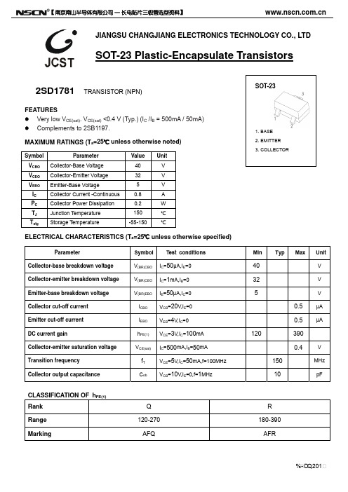
2SD1781贴片三极管规格书
COLLECTOR-EMITTER SATURATION VOLTAGE VCEsat (mV)
COLLECTOR CURRENT IC (mA)
1 1
800
100
10
100
COLLECTOR CURRENT IC (mA)
I
C
—— V BE
β=10
800
=25℃
=100℃
T a
T a
10
1 0.0 300
CAPACITANCE C (pF)
100 1
100
10
10
100
COLLECTOR CURRENT IC (mA)
C / C —— V / V
ob ib
CB EB
Cib
β=10
800
f=1MHz IE=0/ IC=0 Ta=25℃
Cob
1 0.1
250
1
REVERSE VOLTAGE V (V)
P —— T
Ta=25℃
10
1000
2SD1781
h —— I
FE
C
Ta=100℃ Ta=25℃
COMMON EMITTER VCE=3V
10
100
800
COLLECTOR CURRENT IC (mA)
V BEsat
——
I
C
Ta=25℃ Ta=100℃
BASE-EMITTER SATURATION VOLTAGE VBEsat (mV)
Value 40 32 5 0.8 0.2 150
-55-150
Unit V V V A W ℃ ℃
ELECTRICAL CHARACTERISTICS (Ta=25℃ unless otherwise specified)
电磁炉用功率管的型号 代换 参数

电磁炉用功率管的型号代换参数2007年07月28日星期六 12:05大量维修实践表明,电磁炉(灶)内的部分元器件因工作温度较高,工作电流较大,电压较高等,其故障或损坏概率也较高。
其中的场效应功率管损坏率最高。
但由于商业竞争激烈,一般都不随机附带图纸,加之电磁炉所采用的场效应功率管一般均为较新产品,这便给维修带来不便和困难。
下面笔者根据汇集来的相关资料,提供几种常用电磁炉场效应功率管及代换资料供参考。
电磁炉一般均采用N型沟道功率场效应管,其相关参数为BVCBO≥1600V,BVCEO≥1000V,PCM≥100W,ICM≥7A,HFE≥40。
常用的电磁炉用场效应管内部带阻尼二极管的型号有 GT40N150D、GT40T301、SEC·G40N150D、ZON120ND、GT40T101、SQD35JA等。
内部不带阻尼二极管的型号有BT40T101、SGL40N150/150D等。
在维修代换时,若采用不带阻尼二极管的功率场效应管,应在D、S极间加接一只阻尼二极管,该二极管必须是快恢复型阻尼二极管,其耐压应≥1500V。
加接时正极接S 极,负极接D极即可。
参考型号如S5J53、 BY4591500等。
在负载电磁线圈和功率管之间串一只100W的灯泡再通电试机,可以防止烧管。
GT40Q321,FGL40N150D, FGL60N170D, FGA25N120,SK25N120,G40N150D, FGA25N135,1MBH25D--120,GP20B120UD--E,IXGH20N120BDI,以上功率管内部都带阻尼管,耐压都在1200V以上电流在20A以上只要电流相差不多都可以互相代换。
SGW25N120,K15T120。
以上的管子内部不带阻尼,如果要代换一上功率管时可以在电路板上安装2个以上的阻尼二极管耐压1200V以上,电流在8A以上。
电磁炉的关键元器件介绍1、大功率管IGBT(H20T120)说明:(1)、IGBT为电磁炉电路控制核心元器件,使用温度为小于85℃。
分析仪器品牌:Analytical Pressure Regulators,产品名:Brass Tw

Analytical Pressure Regulators• Brass Two-Stage ModelsDescription: This series of high-purity, two-stage regulators is recommended for non-corrosive analytical and process applications where precise pressure control is required. Thisseries is ideally suited for chromatographic carrier gas applications including FID, TCD, ECD,HID, and non-corrosive gas mixtures for analytical instrumentation. These units featurestainless steel diaphragms and bar stock bodies with low internal volume and minimal deadspace.This two-stage design yields a delivery pressure change of less than 0.26/100 psi inletchange, making this one of the most accurate regulators available from full cylinder toempty. An automatic reseating relief valve protects regulator components from overpressurization while dual filters protect the valve seats and extend operating service life.These regulators are nickel-plated to maintain their appearance.• Stainless Steel Diaphragms-eliminates outgassing associated with elastometric diaphragms.• Bar Stock Body-affords low internal volume.• Dual Filters-protect valve seat, extend service life.• Nickel-Plated Brass Body-provides enhanced overall aesthetics, will not tarnish.SpecificationsMaximum Rated Inlet Pressure 3,000 PSIGOutlet Pressure Ranges 0-15, 0-50, 0-100, 0-250 PSIGFlow Capacity Cv=0.079Ambient Operating Temperature -40º F to +165º FDesigned Leak Rate Bubble-Tight (helium)Weight 5 lbsPorts (4) ¼" FNPTInlet ¼" FNPTOutlet ¼" MNPT Instrument ValveDecay Inlet Characteristic 0.26/100 PSI(continued on next page)Analytical Pressure Regulators• Brass Two-Stage Models(continued)MaterialsBody Nickel-Plated BrassBonnet Nickel-Plated BrassSeats Teflon®Diaphragms 316 Stainless SteelGauges 2½" Nickel-Plated BrassFilter 316 Stainless Steel and BronzeValve Stem 316 Stainless SteelValve Spring 316 Stainless SteelOutlet Valve Nickel-Plated BrassTrim Nickel-Plated BrassProductNumber MaterialMaxInletPress.(PSIG)MaxOutletPress.(PSIG)Capacity(scfh @Max Del.Press.)ReliefValveSetting(PSIG)InletGaugeRange(PSIG)DeliveryGaugeRange(PSIG)PriceY12-244A(CGA)Brass3,00015 90 350 0-3,00030" Hg-0-30$355.00 Y12-244B(CGA)Brass3,00050 210 350 0-3,0000-60 $355.00 Y12-244D(CGA)Brass3,000100 310 350 0-3,0000-200 $355.00 Y12-244F(CGA) Brass 3,000 250 400 350 0-3,000 0-400 $355.00ProductNumber Description Price Y99-26120 1/4" FNPT x 1/4" Swagelok®$8.00Y99-26140 1/4" FNPT x 1/8" Swagelok®$8.00 Y99-SMPNLNUT Panel Mount Nut (2 required) $9.00。
制冷接收机低温杜瓦温度监测系统的研制

Vol.6 No14 Dec.,2009天 文 研 究 与 技 术ASTRONOM I CAL RESE ARCH&TECHNOLOGY第6卷 第4期2009年12月CN53-1189/P I SSN1672-7673制冷接收机低温杜瓦温度监测系统的研制3杨 颖1,2,孙正文1,汪小妹1,2(1.中国科学院国家天文台乌鲁木齐天文站,新疆乌鲁木齐830011; 2.中国科学院研究生院,北京100049)摘要:从设计、制作和测试方法方面介绍了一种制冷接收机低温杜瓦温度监测系统。
主要阐述了低温杜瓦对温度监测系统的要求,根据要求合理设计,涉及到各种器件参数的选择以及布局制板等问题,为高精度温度采集系统的硬件设计提供了理论依据。
设计采用多路模拟输入通道即集中采集方式,根据系统的需要划分不同的功能区块进行电路设计。
制作完成的温度监测系统先后经调试校准、实验室模拟测试以及安装在乌鲁木齐25m射电望远镜18c m制冷双极化接收机上测试,各项设计功能都能很好地实现,并且运行可靠。
关键词:低温;杜瓦;温度监测;接收机中图分类号:TP212111 文献标识码:A 文章编号:1672-7673(2009)04-0292-06低温杜瓦是射电望远镜制冷接收机的重要组件,是低温真空腔体,通常有两级低温工作平台,低噪声放大器(LNA)在20K级,物理温度15K左右,微波窗口和正交极化器(OMT)等被安置在70K级上,物理温度60K左右。
温度必须相对稳定,否则会影响接收机的灵敏度,因此需要建立温度监测系统及时了解低温杜瓦内各级平台的温度数据。
本文介绍的低温杜瓦温度监测系统是根据科研设备要求,专门为乌鲁木齐25m射电望远镜18c m制冷双极化接收机研制的,系统由温度传感器、传输线缆、温度采集卡和温度显示卡组成,可同时采集3路温度数据,通过选通开关,分别显示20K、70K 和接收机环境3路温度数据。
1 低温杜瓦温度监测系统的硬件设计温度监测系统的硬件设计主要分为3部分:温度传感器,温度采集卡和温度显示。
- 1、下载文档前请自行甄别文档内容的完整性,平台不提供额外的编辑、内容补充、找答案等附加服务。
- 2、"仅部分预览"的文档,不可在线预览部分如存在完整性等问题,可反馈申请退款(可完整预览的文档不适用该条件!)。
- 3、如文档侵犯您的权益,请联系客服反馈,我们会尽快为您处理(人工客服工作时间:9:00-18:30)。
电气特性
参数 集电极基击穿电压 集电极发射极击穿电压 发射器基地击穿电压 基地发射极饱和电压 集电极 - 发射极饱和电压 集电极截止电流 发射极截止电流 符号
(TA = 25°C,除非另有规定) 测试条件
DC电流传输比
转换频率 输出电容 开启时间 贮存时间 下降时间
BV CBO BV CEO BV EBO V BE(SAT) V CE(SAT) ICBO IEBO hFE1 hFE2 fT C ob t ON tSTG tF
基地发射极电压,V
h - I知道 1000 V =5V Ta=75℃ 25℃ -25℃ V =5V
100
Ta=75℃ 25℃ -25℃ 0.8 1.0 (V) 1.2
10 0.01 0.1
集电极电流,I
1.0 (A)
10
f -I知道 (MHz) V =10V
柯布 - V
f=1MHZ
100 100
增益带宽产品,母头 输出电容,COB(PF)
120 100 6 4 8 1 (T C= 25℃)20(注2) +150 -40 ~ +150
V V V A A W W °C °C
Note1: Duty=1/2, Pw=20ms 注2:当安装在一个40×40×0.7毫米陶瓷电路基板 注3:绝对最大额定值力额定值只和功能设备操作不暗示.
2SD1816
典型特征 Ic -V 5 4 3 Colletcor目前,IC(A) 2 1 0 0 1 2
集电极发射极电压,V
NPN外延平面晶体管
Ic -V 2.0 1.6 8mA 7mA 6mA 5mA ColletcorCurrent, Ic (A) 1.2 4mA 0.8 0.4 0 4 (V) 5 0 10 20
见测试电路 见测试电路 见测试电路
MIN 120 100 6
TYP
最大单位
0.9 150
70 40 180 40 100 900 50
1.2 400 1 1 400
V V V V mV µA µA
MHz pF ns ns ns
^ h分类
秩 范围
R 100 - 200
S 140 - 280
T 200 - 400
10 0.1 Colletcor电流Ic(A) , 1.0 1.0 10 100 (V) Colletcor基极电压,V
3 of 4
QW-R209-011,B
芯片中文手册,看全文,戳
2SD1816
典型特征(续) V I /I =10 (mV) 1000 - I知道
NPN外延平面晶体管
4 of 4
QW-R209-011,B
芯片中文手册,看全文,戳
2SD1816
绝对最大额定值
参数 集电极基极电压 集电极 - 发射极电压 发射极基极电压 集电极电流 集电极耗散功率 结温 储存温度
NPN外延平面晶体管
(Ta =25℃ )
符号 额定值 单元
V CBO V CEO V EBO DC
脉冲(注1)
IC PD TJ T STG
Q 70 -140
测试电路
PW=20μS
占空比≒1%
I B1 RB I B2 50 VR + 100µ -5V Ic=10, I B1= -10, I B2=2A
单位(电阻:Ω,电容:F) 产量
INPUT
+ 470 µ 50V
2 of 4
QW-R209-011,B
芯片中文手册,看全文,戳
集电极发射极电压,V
100mA 80mA 90 mA 70mA 60mA
AA 50m m 40 A 30m 20mA 10mA 5mA 2mA I =0 3
3mA 2mA 1mA I =0 30 40 (V) 50
Ic -V 5 4 3 Colletcor目前,IC(A) 2 DC电流增益,H 1 0 0 0.2 0.4 0.6
FE1
IC =10µA, I E =0 IC =1mA, R B=∞ IE =10µA, I C=0 IC = 2A, I B =0.2A IC = 2A, I B=0.2A V CB = 100 V, I E =0 V EB = 4V, I C=0 V CE = 5V, I C = 0.5A V CE =5V, I C = 3A V CE =10V, I C =0.5A V CB =10V, I E =0A, f =1MHz
集电极耗散,P
P -Ta 25 (W) 20
DC D C 1.0 (最佳 O a= CollectorCurrent, I 25 C鼠 pe ℃ ion ラ吨 ) 离子 0.1
(T c= 25 Tc=25℃
一个脉冲
℃
)
5 1 0
无散热片
0.01
1.0
10
100 (V)
0
20
40
60
80 100 120 140 160 (℃)
Colletcor到发射极电压,V
环境温度,钽
UTC不承担由于使用产品超过,即使是瞬间值,设备故障不承担任何责任,额定数值(例如最大额 定值,工作环境范围或其他参数)任何产品规格和描述或此处包含所有UTC产品上市. UTC产 品并非设计用于生命支持设备,装置或在这些产品故障可合理预期会导致人身伤害系统.严禁复制 全部或部分未经版权拥有者事先书面同意.本文件中不构成任何报价或合同一部分信息,被认为 是准确可靠,恕不另行通知可随时更改.
V 10 (V)
- I知道 I /I =10
集电极到发射极
100
饱和电压,V
Ta=75℃
25℃ -25℃
基地发射极 饱和电压,V
1.0
钽= -25℃
25℃ 75℃
0.01
0.1
集电极电流I
1.0 , (A)
10
0.01
0.1
集电极电流I
1. 0 , (A)
10
ASO 10 Icp (A) Ic 1ms 10ms 100ms 15 10
芯片中文手册,看全文,戳
2SD1816
高电流SWITCHIG 应用
NPN外延平面晶体管
1
特征
TO-252
*低集电极 - 发射极饱和电压 * h线性好 FE *套小巧玲珑包装便利紧凑. *高氟 T *开关速度快
1
TO-251
*无铅电镀产品编号:2SD1816L
订购信息
订单号 正常 无铅电镀 包 引脚分配 填料 管
2SD1816-x-TM3-F-T 2SD1816-x-TN3-F-K 2SD1816-x-TN3-F-R 注:X:等级,是指h分类 2SD1816L-x-TM3-F-T
2SD1816L-x-TM3-F-T 2SD1816L-x-TN3-F-K 2SD1816L-x-TN3-F-R FE1.
(1)包装类型 (2)引脚分配 (3)包装类型
TO-251 TO-252 TO-252
1 B B B
2 C C C
3 E E E
Bulk
带盘
(1)K:散装,T:管R:带卷轴 (2)参考引脚分配
(4)Rank (5)铅电镀
(3) TM3: TO-251, TN3: TO-252 (4)×:指h分类 (5)L:无铅电镀,空白:铅/锡
4之1
QW-R209-011,B