MC14513B_IcpdfCom
IP1203PBF,IP1203TRPBF,IP1203PBF,IP1203TRPBF, 规格书,Datasheet 资料
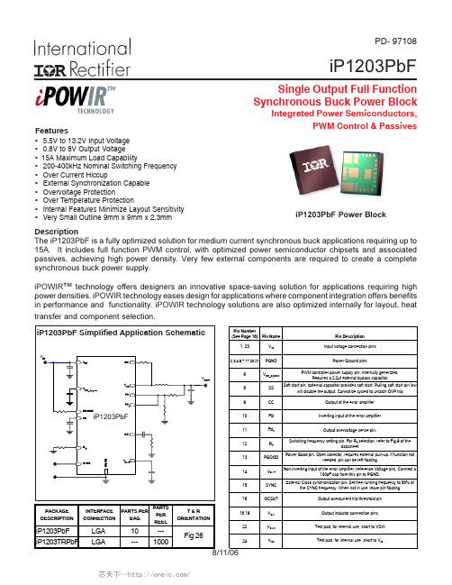
iP1203PbF Power BlockDescriptionThe iP1203PbF is a fully optimized solution for medium current synchronous buck applications requiring up to 15A. It includes full function PWM control, with optimized power semiconductor chipsets and associated passives, achieving high power density. Very few external components are required to create a complete synchronous buck power supply.iPOWIR ™ technology offers designers an innovative space-saving solution for applications requiring high power densities. iPOWIR technology eases design for applications where component integration offers benefits in performance and functionality. iPOWIR technology solutions are also optimized internally for layout, heat transfer and component selection.• 5.5V to 13.2V Input Voltage •0.8V to 8V Output Voltage • 15A Maximum Load Capability•200-400kHz Nominal Switching Frequency •Over Current Hiccup•External Synchronization Capable •Overvoltage Protection•Over Temperature Protection•Internal Features Minimize Layout Sensitivity •Very Small Outline 9mm x 9mm x 2.3mmFeaturesSingle Output Full Function Synchronous Buck Power BlockIntegrated Power Semiconductors,PWM Control & PassivesiP1203PbFPD- 97108iP1203PbFAbsolute Maximum RatingsRecommended Operating ConditionsElectrical Specifications @ V IN = 12VAll specifications @ 25°C (unless otherwise specified)iP1203PbF Electrical Specifications (continued)iP1203PbF ArrayFig. 1:iP1203PbF Internal Block DiagramiP1203PbFFig. 2: Power Loss vs. Current0102030405060708090100110120130Case Temperature (°C)102030405060708090100110120130PCB Temperature (°C)0246810121416O u t p u t C u r r e n t (A )Tx51015Output Current (A)0123456P o w e r L o s s (W )iP1203PbFFig. 6: Normalized Power Loss vs. FrequencyFig. 4: Normalized Power Loss vs. V INFig. 5: Normalized Power Loss vs. V OUTTypical Performance CurvesFig. 7: Normalized Power Loss vs. Inductance0.40.81.21.62.0 2.4Output Inductance (µH)0.961.001.041.081.121.161.201.24P o w e r L o s s (N o r m a l i z e d )-1.00.01.02.03.04.05.06.0SOA Temp Adju stment (°C)Fig. 8: Nominal Overcurrent Threshold Setting200250300350400Swiching Frequency (kHz)0.9601.0001.0401.0801.120P o w e r L o s s (N o r m a l i z e d )-0.50.00.51.01.5SOA Temp Adju stment (°C)681012141618202224Overload Current (A)525456585105125145165185205ROC-SET (kO hms) for 5.5Vin510152025303540455055R O C -S E T (k O h m s ) f o r 12V i n20253035404550R T (kOhms)200220240260280300320340360380400S w i t c h i n g F r e q u e n c y (k H z )0.81.62.43.24.04.85.66.47.28.0Output Voltage (V)0.920.961.001.041.081.121.161.201.241.281.321.36P o w e r L o s s (N o r m a l i z e d )-2-1012345678910SOA Temp Adjustment (°C)567891011121314Input Voltage (V)0.960.981.001.021.041.06P o w e r L o s s (N o r m a l i z e d )-1.0-0.50.00.51.01.5SOA Temp Adjustment (°C)iP1203PbFAdjusting the Power Loss and SOA Curves for Different Operating ConditionsTo make adjustments to the power loss curves in Fig. 2, multiply the normalized value obtained from the curves in Figs. 4,5, 6 or 7 by the value indicated on the power loss curve in Fig. 2. Then if multiple adjustments are required, multiply all of the normalized values together, then multiply that product by the value indicated on the power loss curve in Fig. 2. The resulting product is the final power loss based on all factors. See example no. 1.To make adjustments to the SOA curve in Fig. 3, determine your maximum PCB Temp & Case Temp at the maximum operating current of each iP1203PbF . Then, add the correction temperature from the normalized curves in Figs. 4, 5, 6 or 7 to the T X axis intercept (see procedure no. 2 above) in Fig. 3. When multiple adjustments are required, add all of the temperatures together, then add the sum to the T X axis intercept in Fig. 3. See example no. 2.Operating Conditions for the following examples:Output Current = 12A Input Voltage = 13.2V Inductor = 0.6µHOutput Voltage = 1.2VSw Freq= 400kHzExample 1) Adjusting for Maximum Power Loss:(Fig. 2)Maximum power loss = 4.1W(Fig. 4)Normalized power loss for input voltage ≈ 1.025(Fig. 5)Normalized power loss for output voltage ≈ 0.97(Fig. 6)Normalized power loss for frequency ≈ 1.08(Fig. 7)Normalized power loss for inductor value ≈ 1.08Adjusted Power Loss = 4.1 x 1.025 x 0.97 x 1.08 x 1.08 ≈ 4.75WApplying the Safe Operating Area (SOA) CurveThe SOA graph incorporates power loss and thermal resistance information in a way that allows one to solve for maximum current capability in a simplified graphical manner. It incorporates the ability to solve thermal problems where heat is drawn out through the printed circuit board and the top of the case.Procedure1)Draw a line from Case Temp axis at T CASE to the PCBTemp axis at T PCB .2)Draw a vertical line from the T X axis intercept to the SOAcurve. (see AN-1047 for further explanation of T X )3)Draw a horizontal line from the intersection of the verticalline with the SOA curve to the Y axis. The point at which the horizontal line meets the y-axis is the SOA current.4)If no top sided heatsinking is available, assume T CASEtemperature of 125°C for worst case performance.120102030405060708090100110102030405060708090100110120PCB Temperature (ºC)O u t p u t C u r r e n t (A )Case Temperature (ºC)iP1203PbFExample 2) Adjusting for SOA Temperature:Assuming T CASE = 110°C & T PCB = 90°C for both outputsOutput1(Fig. 4)Normalized SOA Temperature for input voltage ≈ +0.7°C(Fig. 5)Normalized SOA Temperature for output voltage ≈ -0.75°C (Fig. 6)Normalized SOA Temperature for frequency ≈ +1.0°C (Fig. 7)Normalized SOA Temperature for inductor value ≈ +2.0°CT X axis intercept temp adjustment = +0.5°C - 0.75°C + 1.0°C +2.0°C ≈ +2.75°CThe following example shows how the SOA current is adjusted for a T X change of +2.75°C and output is in SOAFig. 10: Power Loss Test Circuit120102030405060708090100110102030405060708090100110120PCB Temperature (ºC)O u t p u t C u r r e n t (A )Case Temperature (ºC)TXFig. 11: Recommended PCB Footprint (Top View)iP1203PbFThe operating switching frequency (f SW ) range of iP1203PbF is 200 kHz to 400 kHz. The desired fre-quency is set by placing an external resistor to the R T pin of the iP1203PbF . See Fig. 9 for the proper resistor value.The iP1203PbF is capable of accepting an external digital synchronization signal. Synchronization will be enabled by the rising edge clock. The free run-ning oscillator frequency is twice the switching fre-quency. During synchronization, R T is selected such that the free running frequency is 20% below the synchronization frequency. The maximum synchro-nization frequency that iP1203PbF can accept is 800kHz. Note that the actual switching frequency is half the synchronization frequency.iP1203PbF User s Design GuidelinesThe iP1203PbF is a single output 15A power block consisting of optimized power semiconductors, PWM control and its associated passive components. It is based on a synchronous buck topology and offers an optimized solution where space, efficiency and noise caused by parasitics are of concern. The power block operates with fixed frequency voltage mode control. The iP1203PbF components are integrated in a land grid array (LGA) package.V IN / Enabling the OutputThe input operating voltage range of the iP1203PbF is 5.5V to 13.2V.The iP1203PbF output is turned on upon application of input voltage. The V IN slew rate should not exceed 50mV/µs. The converter can also be turned on and off by releasing or pulling the SS pin low through a logic level MOSFET, the drain of which connects to the soft start pin (see Fig.12). This feature can be useful if sequencing or different start-up timing of dif-ferent system outputs are required. In situations where the output has undergone a latched shutdown due to overvoltage, cycling Vin will reset the output. Cycling soft start pin will not unlatch the output.Soft StartThe Soft Start function provides a controlled rise of the output voltage, thus limiting the inrush current.The soft start function has an internal 25µA +/-20%current source that charges the external soft start capacitor C ss up to 3V. During power-up, the output voltage starts ramping up only after the charging volt-age across the C ss capacitor has reached a 0.8Vtyp threshold, as shown in Fig. 13.Fig. 13: Power Up Threshold3V0.8VtypV Css V OUTFig.12: Soft Start/Enable CircuitFrequency and SynchronizationOvercurrent Protection HICCUPThe overcurrent protection function of the iP1203PbF offers a hiccup feature. During overloads, when the overcurrent trip threshold is reached, the power sup-ply output shuts down and attempts to restart (out-put HICCUP mode). The time duration between the shutdown of the output and the restart is determined by the time it takes to discharge the soft start ca-pacitor. Typically, the discharge time of the soft start capacitor is 10 times the charge time. The duty cycle of the hiccup process is typically 5%. The output will stay in hiccup indefinitely until the overload is re-moved. The typical overcurrent trip threshold of the device is internally set at 30A. The overcurrent shut-down / HICCUP threshold is about ±30% accurate.The iP1203PbF overcurrent shutdown and HICCUP threshold can be set externally by adding R OCSET re-sistor from OCSET pin. Refer to Fig.8 for R OCSET se-lection.Overvoltage Protection (OVP)Overvoltage is sensed through output voltage sense pin FB s . The OVP threshold is set to 115% of the output voltage. Upon overvoltage condition, the OVP forces a latched shutdown. In this mode, the upper FET turns off and the lower FET turns on, thus crowbaring the output. Reset is performed by recy-cling the input voltage. Overvoltage can be sensed by either connecting FB s to its corresponding output through a separate output voltage divider resistor network, or it can be connected directly to its corre-sponding feedback pin FB. For Type III control loop compensation, FB s should be connected through voltage dividers only.Refer to the iP1203PbF Design Procedure section on how to set the OVP trip threshold.PGOODThis is an output voltage status signal that is open collector and is pulled low when the output voltage falls below 85% of the output voltage. High state in-dicates that outputs are in regulation. The PGOOD pin can be left floating if not used.Thermal ShutdownThe iP1203PbF provides thermal shutdown. The threshold typically is set to 140°C. When the trip threshold is exceeded, thermal shutdown turns the output off. Thermal shutdown is not latched and au-tomatic restart is initiated when the sensed tempera-ture drops to the normal range.Only a few external components are required to com-plete a dual output synchronous buck power supply using iP1203PbF. The following procedure will guide the designer through the design and selection pro-cess of these external components.A typical application for the iP1203 is:V IN = 12V, V OUT = 1.5V, I OUT = 15A, f sw = 300kHz, V p-p == 50mVSetting the Output VoltageThe output voltage of the iP1203PbF is set by the 0.8V reference Vand external voltage dividers.Fig. 14: Typical Scheme for Output Voltage Setting V OUT is set according to equation (1):V OUT = V REF x (1 + R 2 /R 5 ) (see Fig. 14)(1)Setting R 2 to 1K, V OUT to 1.5V and V REF to 0.8V, will result in R 5= 1.14 Kohms. Final values can be se-lected according to the desired accuracy of the out-put.To set the output voltage for Type III compensation,refer to equation (24) in Type III compensation sec-tion.iP1203PbF Design ProcedureSetting the Overvoltage TripThe output of the iP1203 will shut down if it experi-ences a voltage in the range of 115% of V OUT . The overvoltage sense pin FB s is connected to the out-put through voltage dividers, R26 and R27 (Fig. 14),and the trip setpoint is programmed according to equation (1). A separate overvoltage sense pin FB s is provided to protect the power supply output if for some reason the main feedback loop is lost (for in-stance, loss of feedback resistors). An optional 100pF capacitor (C14) is used for delay and filtering.If this redundancy is not required and if a Type II con-trol loop compensation scheme is utilized, FB s pin can be connected to FB.Selecting the Soft-Start CapacitorThe soft start capacitor C ss is selected according to equation (2):t ss = 40 x C ss(2)where,t ss is the output voltage ramp time in milliseconds,and C ss is the soft start capacitor in µF.A 0.1µF capacitor will provide an output voltage ramp-up time of about 4ms.Input Capacitor SelectionThe switching currents impose RMS current require-ments on the input capacitors. Equation (3) allows the selection of the input capacitors.where, I out is the output current, and D is the duty cycle and is expressed as:D = V OUT / V IN .For the above example D= 0.13 and, using equation (3) the capacitor rms current yields 5.0A.For Type II compensation,(3))1(D D I I out RMS −=For better efficiency and low input ripple, select low ESR ceramic capacitors. The amount of the capaci-tors is determined based on the rms rating. In the above example, a total of 3 x 22µF, 2A capacitors will be required to support the input rms current.Output Capacitor C O SelectionSelection of the output capacitors depends on two factors:a. Low effective ESR for ripple and load transient re-quirementsTo support the load transients and to stay within a specified voltage dip ∆V due to the transients, ESR selection should satisfy equation (4):R ESR ≤ ∆V / I Loadmax(4)Where,I Loadmax is the maximum load current.If output voltage ripple is required to be maintained at specified levels then the expression in equation (5) should be used to select the output capacitors.R ESR ≤ V p-p / I ripple(5)Where,V p-p is the peak to peak output ripple voltage .I ripple is the inductor peak-to peak ripple current.In addition, the voltage ripple caused by the output capacitor needs to be significantly smaller than the ripple caused by the ESR of the capacitor. Use equa-tion (6) to satisfy this requirement.If the inductor current ripple I ripple is 30% of I OUT1, the 50mV peak to peak output voltage ripple requirement will be met if the total ESR of the output capacitors is less than 11m Ω. This will require 2 x 470µF POSCAP capacitors. Additional ceramic capacitors can be added in parallel to further reduce the ESR. Care should be given to properly compensate the control loop for low output capacitor ESR values.When selecting output capacitors, it is important to consider the overshoot performance of the power sup-ply. If the amount of capacitance is not adequate, then,when unloading the output, the magnitude of the over-shoot due to stored inductor energy, and depending on the speed of the response of the control loop, can exceed the overvoltage trip threshold of the iP1203PbF and can cause undesirable shutdown of the output. The magnitude of the overshoot should be kept below 1.125V OUT . To prevent the overshoot from tripping the output a delay can be added by in-stalling capacitor C14 as shown in Fig.14.b. StabilityThe value of the output capacitor ESR zero frequency f esr plays a major role in determining stability. f esr is calculated by the expression in equation (7).f ESR = 1 / (2 π x R ESR x C O )(7)Details on how to consider this parameter to design for stability are outlined in the control loop compen-sation section of this datasheet.Inductor L O SelectionInductor selection is based on trade-offs between size and efficiency. Low inductor values result in smaller sizes, but can cause large ripple currents and lower efficiency. Low inductor values also benefit the tran-sient performance.The inductor L o is selected according to equation (8):L O = V out x (1 - D) / (f sw x I ripple )(8)For the above example, and for I ripple of 30% of I OUT , L O is calculated to be 1.0µH.The core must be selected according to the peak of maximum output current.(6)ESRs o R f C ××>π210Control Loop CompensationThe iP1203PbF feedback control is based on single loop voltage mode control principle.The goal in the design of the compensator is to achieve the highest unity gain (0 db) crossover fre-quency with sufficient phase margin for the closed loop transfer function. The LC filter of the power sup-ply introduces a double pole with 40db/dec slope and 180° phase lag. The 180° phase contribution from the LC filter is the source of instabilty.The resonant frequency of the LC filter is expressed by equation (9):(9)The error amplifier of the iP1203PbF PWM controlleris transconductance amplifier, and its output is avail-able for external compensation.Two types of compensators are studied in this sec-tion. The first one is called Type II and it is used to compensate systems the ESR frequency f esr (equa-tion 7) of which is in the midfrequency range and Type III that can be used for any type of output capacitors and have a wide range of f esr .For output voltage settings less than 1.0V that use low ESR ceramic capacitors, it is recommended that the unity gain crossover frequency be set around 20kHz to maintain stable operation.where, g m is the transconductance of the error am-plifier.(12)Follow the steps below to determine the feedback loop compensation component values:1. Select a zero db crossover frequency f 0 in the range of 10% to 20% of the switching frequency f sw.)(2 / 1 00C L f LC ×=πType IIFrom Fig.15 the transfer function H(s) of the error amplifier is given by (10):(10)The term s represents the frequency dependence ofthe transfer function.The Type II controller introduces a gain and a zero expressed by equations (11) and (12):9199192551)(C sR C sR R R R g s H m +×+×=91921C R f z ××=πFig. 15: Typical Type II Compensation and its Gain Plot(11)19255)(R R R R g s H m ×+×=3. Place a zero at 75% of f LC to cancel one of the LC filter poles.oo z C L f ××=π2175.04. Calculate C 9 using equations (12) and (14)Calculation of the compensation components based on the example above, yields:f LC = 5.0kHz f z = 3.8kHzf 0 = 45kHz (15% of 300kHz)f esr = 14kHz, per equation (7) using R esr = 12m Ω.R 19 = 2.49K C 9 = 18nFSometimes, a pole f p2 is added at half the switching frequency to filter the switching noise. This is done by adding a capacitor C opt in Fig.15 from the output of the error amplifier (CC pin of iP1203PbF) to ground.This pole is given by equation (15):C opt is found from equation (16) by rearranging the terms in equation (15) and by setting f p2 = f sw / 2:(16)Fig. 16: Typical Type III Compensation and its Gain PlotType IIIThe Type III compensation scheme allows the use of any type of capacitors with ESR frequency of any range. This scheme suggests a double pole double zero compensation and requires more components around the error amplifier to achieve the desired gain and phase margins. Fig. 13 represents the Type III compensation network for iP1203PbF.The transfer function of the Type III compensator is given by equation (17)2. Calculate R 5 using equation (13):Where,V IN = Maximum input voltagef 0 = Error amplifier zero crossover frequency f esr = Output capacitor C o zero frequency f LC = Output frequency resonant filterg m = Error amplifier transconductance. Use 2mS for g m .V ramp = Oscillator ramp voltage. Use 1.25V for V ramp(14)(13)(15)optp C R f ××=19221π19221R f C p opt ××=π)1()1()1()1(1)(8217208292092C sR C sR C sR C sR C sR s H +×++×+×=(17)mLC esr in ramp g R R R f f f V V R 115252019×+××××=R 210Vref V o- VrefMore than one iteration may be required to calculate the values of the compensation components if cross-over frequencies higher than the range specified in step 1 are required (for higher bandwidths and faster transient response performance). To ensure stability a phase margin greater than 45° should be achieved.Refer to AN-1043 for more detailed compensation techniques using Transconductance Amplifiers.7. Place the second pole f p2 at or near f esr of the out-put capacitor C o and determine the value of R 21 fromequation (19). Make sure R 21 <8. Use equation (24) to calculate R 5.R 5 = R 2 x (24)The crossover frequency f 0 for Type III compensa-tion is represented by equation (23):Follow the steps below to determine the feedback loop compensation component values:1. Select a zero db crossover frequency f 0 in the range of 10% to 20% of the switching frequency f sw.2. Select R 20~ 10k Ω3. Place the first zero f z1 at 75% of the resonant fre-quency f LC of the output filter.Determine C 9 from equation (21).4. Place a third pole f P3 at or near the switching fre-quency f SW .Select C7 such that C 7 <5. Calculate C 8 from equation (23).6. Place the second zero at 125% of the resonant frequency f LC of the output filter. Calculate R 2 using equation (22).109C The frequencies of the three poles and the two zeros of the Type III compensation scheme are represented by the following equations:f p1= 0(18)(19)(21)(20)821221C R f p ××=π720321C R f p ××=π920121C R f z ××=π82221C R f z ××=π008200211C L C R V V f IN ramp××××××=π(22)(23)Typical WaveformsCh1: Switching node, 400kHzCh2: 800kHz external synchronizationFig. 17: iP1203PbF Outputs Synchronized to800kHz Ch1: Output voltage, 500mV/divCh3: Output current, 10A/divFig. 18: iP1203PbF Output Hiccup, Due to Over-loadCh1: Output voltage, 100mV/div acCh3: Load current, 5A/divFig. 19: iP1203PbF Transient Response Load Step 1A to 12A Ch1: Output voltage, 100mV/div acCh3: Load current, 5A/divFig. 20: iP1203PbF Transient Response Load Step12A to 0ACh1: FB s input, 200mV/divCh2: Output voltage, 1V/divFig. 21: iP1203PbF Overvoltage Trip. Output Voltage Turns Off When Voltage at FB s Pin Exceeds 15% of FB (0.8V)For stable and noise free operation of the whole power system, it is recommended that the design-ers use the following guidelines:1. Follow the layout scheme presented in Fig. 23. Make sure that the output inductor L is placed as close to iP1203PbF as possible to prevent noise propagation that can be caused by switching of power at the switching node Vsw, to sensitive cir-cuits.2. Provide a mid-layer solid ground plane with con-nections to the top layer through vias. The PGND pads of iP1203PbF also need to be connected to the same ground plane through vias.3. To increase power supply noise immunity, place input and output capacitors close to one another, as shown in the layout diagram. This will provide short high current paths that are essential at the ground terminals.4. Although there is a certain degree of VIN bypass-ing inside the iP1203PbF, the external input decoupling capacitors should be as close to the device as pos-sible.5. The feedback track from the output VOUTto FB should be routed as far away from noise generating traces as possible.6. The compensation components and the Vref by-pass capacitor should be placed as close as pos-sible to their corresponding iP1203PbF pins, away from noise generating traces.7. Refer to IR application note AN-1029 (Optimizinga PCB Layout for an iPOWIR Technology Design) to determine what size vias and copper weight and thickness to use when designing the PCB.8. Place the overcurrent threshold setting resistors ROCSETclose to the iP1203PbF block at the corre-sponding connection node.Layout GuidelinesFig. 24: Typical Application Schematic 21This paper describes how to optimize the PCB layout design for both thermal and electrical performance. This includes placement, routing, and via interconnect suggestions.AN-1030: Applying iPOWIR Products in Your Thermal EnvironmentThis paper explains how to use the Power Loss vs Current and SOA curves in the data sheet to validate if the operating conditions and thermal environment are within the Safe Operating Area of the iPOWIR product.AN-1043: Stabilize the Buck Converter with Transconductance AmplifierThis paper explains how to stabilize a buck converter for Type II and Type III control loop compensation using transconductance amplifiers.AN-1047: Graphical solution to two branch heatsinking Safe Operating AreaThis paper is a suppliment to AN-1030 and explains how to use the double side Power Loss vs Current and SOA curves in the data sheet to validate if the operating conditions and thermal environment are within the Safe Operating Area of the iPOWIR product.AN-1028: Recommended Design, Integration and Rework Guidelines for International Rectifier s iPOWIR Technology BGA and LGA PackagesThis paper discusses optimization of the layout design for mounting iPOWIR BGA and LGA packages on printed circuit boards, accounting for thermal and electrical performance and assembly considerations.Topics discussed includes PCB layout placement, routing, and via interconnect suggestions, as well as soldering, pick and place, reflow, cleaning and reworking recommendations.芯天下--/22iP1203PbFFig. 27: Part Marking芯天下--/ 23This product has been designed and qualified for the industrial market.IR WORLD HEADQUARTERS: 233 Kansas St., El Segundo, California 90245, USA Tel: (310) 252-7105TAC Fax: (310) 252-7903Visit us at for sales contact information .Data and specifications subject to change without notice.8/06Fig.28: Recommended Solder Profile and Stencil Design芯天下--/。
MC14433 CD4511 MC1413 MC1403 应用数字电压表电路图-中文资料-引脚功能--管脚说明-数显电压

MC14433 CD4511 MC1413 MC1403 应用数字电压表电路图-中文资料-引脚功能--管脚说明-数显电压数字显示电压表将被测模拟量转换为数字量,并进行实时数字显示。
该系统(如图1 所示)可采用MC14433—位A/D 转换器、MC1413七路达林顿驱动器阵列、CD4511 BCD到七段锁存-译码-驱动器、能隙基准电源MC1403和共阴极LED发光数码管组成。
本系统是位数字电压表, 位是指十进制数0000~1999。
所谓3位是指个位、十位、百位,其数字范围均为0~9,而所谓半位是指千位数,它不能从0变化到9,而只能由0变到l,即二值状态,所以称为半位。
各部分的功能如下:位A/D转换器(MC14433):将输入的模拟信号转换成数字信号。
基准电源(MC1403):提供精密电压,供A/D 转换器作参考电压。
译码器(MC4511):将二—十进制(BCD)码转换成七段信号。
驱动器(MC1413):驱动显示器的a,b,c,d,e,f,g七个发光段,驱动发光数码管(LED)进行显示。
显示器:将译码器输出的七段信号进行数字显示,读出A/D转换结果。
工作过程如下:位数字电压表通过位选信号DS1~DS4进行动态扫描显示,由于MC14433电路的A/D转换结果是采用BCD码多路调制方法输出,只要配上一块译码器,就可以将转换结果以数字方式实现四位数字的LED发光数码管动态扫描显示。
DS1~DS4输出多路调制选通脉冲信号。
DS选通脉冲为高电平时表示对应的数位被选通,此时该位数据在Q0~Q3端输出。
每个DS选通脉冲高电平宽度为18个时钟脉冲周期,两个相邻选通脉冲之间间隔2个时钟脉冲周期。
DS和EOC 的时序关系是在EOC 脉冲结束后,紧接着是DS1输出正脉冲。
以下依次为DS2,DS3和DS4。
其中DS1对应最高位(MSD),DS4则对应最低位(LSD)。
在对应DS2,DS3和DS4选通期间,Q0~Q3输出BCD全位数据,即以8421码方式输出对应的数字0~9.在DS1选通期间,Q0~Q3输出千位的半位数0或l及过量程、欠量程和极性标志信号。
MC14583_IcpdfCom
MC14583B 1
ÎÎÎÎÎÎÎÎÎÎÎÎÎÎÎÎÎÎÎÎÎÎÎÎÎÎÎÎÎÎÎÎÎÎ ÎÎÎÎÎÎÎÎÎÎÎÎÎÎÎÎÎÎÎÎÎÎÎÎÎÎÎÎÎÎÎÎÎÎ ÎÎÎÎÎÎÎÎÎÎÎÎÎÎÎÎÎÎÎÎÎÎÎÎÎÎÎÎÎÎÎÎÎÎ ÎÎÎÎÎÎÎÎÎÎÎÎÎÎÎÎÎÎÎÎÎÎÎÎÎÎÎÎÎÎÎÎÎÎ
LOGIC DIAGRAM
POSITIVE A NEGATIVE A 6 5 7 COMMON A Ain 9
2 4 Aout
3
1
TRUTH TABLE
11 Aout 3–STATE OUTPUT DISABLE 13 14 EXCLUSIVE OR 0 0 0 0 1 1 1 1 Inputs A B 0 0 1 1 0 0 1 1 Outputs 0 0 1 1 1 1 0 0 Dis Aout Aout Bout Bout 0 0 Z 0 Z 1 0 1 0 1 0 0 Z 1 Z 1 0 1 1 0 0 1 0 1 1 1 1 1 Z 0 Z 0 0 0 1 1 Z 1 Z 0
Symbol VDD Parameter DC Supply Voltage L SUFFIX CERAMIC CASE 620
P SUFFIX PLASTIC CASE 648
D SUFFIX SOIC CASE 751B
ÎÎÎÎÎÎÎÎÎÎÎÎÎÎÎÎÎÎÎÎÎ ÎÎÎÎÎÎÎÎÎÎÎÎÎÎÎÎÎÎÎÎÎ ÎÎÎÎÎÎÎÎÎÎÎÎÎÎÎÎÎÎÎÎÎ ÎÎÎÎÎÎÎÎÎÎÎÎÎÎÎÎÎÎÎÎÎ
MOTOROLA
SEMICONDUCTOR TECHNICAL DATA
MC14583B Dual Schmitt Trigger
The MC14583B is a dual Schmitt trigger constructed with complementary P–channel and N–channel MOS devices on a monolithic silicon substrate. Each Schmitt trigger is functionally independent except for a common 3–state input and an internally–connected Exclusive OR output for use in line receiver applications. Trigger levels are adjustable through the positive, negative, and common terminals with the use of external resistors. Applications include the speed–up of a slow waveform edge in interface receivers, level detectors, etc. • • • • Diode Protection on All Inputs Supply Voltage Range = 3.0 Vdc to 18 Vdc Single Supply Operation Capable of Driving Two Low–power TTL Loads or One Low–power Schottky TTL Load Over the Rated Temperature Range • Resistor Adjustable Trigger Levels MAXIMUM RATINGS* (Voltages Referenced to VSS)
MC1455B中文资料
117 Vac/60 Hz
10 k 0.1 mF
5 0.01 mF
1.0 k
38
4
6R
2 MC1455 7
1 1.0 mF
MT2 20 M G
C −10 V
Load MT1
1N4003
MARKING DIAGRAMS
8 1
SOIC−8 D SUFFIX CASE 751
VCC−VOH (Vdc)
MC1455, MC1455B, NCV1455B
150
10
ICC, SUPPLY CURRENT (mA)
125
Operating Temperature Range (Ambient) MC1455B MC1455 NCV1455B
VCC
+18
Vdc
I7
200
mA
PD
625
mW
5.0
mW/°C
PD
625
mW
160
°C/W
TA
°C
−40 to +85
0 to +70
−40 to +125
Maximum Operating Die Junction Temperature
1N4740
3.5 k
− 10
mF
250 V +
Figure 1. 22 Second Solid State Time Delay Relay Circuit
VCC 8
5k 6 Threshold
5 Control Voltage
5k
Trigger
2 5k
+ Comp −A
mc145151_2_5_6_7_8
MC145151–2 through MC145158–21MOTOROLAMC145151–2 through MC145158–25MC145151–2 through MC145158–29MC145151–2 through MC145158–213MC145151–2 through MC145158–2MOTOROLA15OUTPUT PINSPD outPhase Detector A Output (Pin 6)Three–state output of phase detector for use as loop–error signal. Double–ended outputs are also available for this pur-pose (see φV and φR ).Frequency f V > f R or f V Leading: Negative Pulses Frequency f V < f R or f V Lagging: Positive PulsesFrequency f V = f R and Phase Coincidence: High–Imped-ance State φR , φVPhase Detector B Outputs (Pins 4, 3)These phase detector outputs can be combined externally for a loop–error signal. A single–ended output is also avail-able for this purpose (see PD out ).If frequency f V is greater than f R or if the phase of f V is leading, then error information is provided by φV pulsing low.φR remains essentially high.If the frequency f V is less than f R or if the phase of f V is lagging, then error information is provided by φR pulsing low.φV remains essentially high.If the frequency of f V = f R and both are in phase, then both φV and φR remain high except for a small minimum time period when both pulse low in phase.MCDual–Modulus Prescale Control Output (Pin 8)Signal generated by the on–chip control logic circuitry for controlling an external dual–modulus prescaler. The MC level will be low at the beginning of a count cycle and will remain low until the ÷ A counter has counted down from its pro-grammed value. At this time, MC goes high and remains high until the ÷ N counter has counted the rest of the way down from its programmed value (N – A additional counts since both ÷ N and ÷ A are counting down during the first portion of the cycle). MC is then set back low, the counters preset totheir respective programmed values, and the above se-quence repeated. This provides for a total programmable divide value (N T ) = N P + A where P and P + 1 represent the dual–modulus prescaler divide values respectively for high and low MC levels, N the number programmed into the ÷ N counter, and A the number programmed into the ÷ A counter.LDLock Detector Output (Pin 9)Essentially a high level when loop is locked (f R , f V of same phase and frequency). LD pulses low when loop is out of lock.SW1, SW2Band Switch Outputs (Pins 14, 15)SW1 and SW2 provide latched open–drain outputs corre-sponding to data bits numbers one and two. These outputs can be tied through external resistors to voltages as high as 15 V, independent of the V DD supply voltage. These are typically used for band switch functions. A logic 1 causes the output to assume a high–impedance state, while a logic 0causes the output to be low.REF outBuffered Reference Oscillator Output (Pin 17)Buffered output of on–chip reference oscillator or externally provided reference–input signal.POWER SUPPLYV DDPositive Power Supply (Pin 5)The positive power supply potential. This pin may range from + 3 to + 9 V with respect to V SS .V SSNegative Power Supply (Pin 7)The most negative supply potential. This pin is usually ground.MC145151–2 through MC145158–217MOTOROLAOUTPUT PINSPD outPhase Detector A Output (Pin 5)This single–ended (three–state) phase detector output pro-duces a loop–error signal that is used with a loop filter to con-trol a VCO.Frequency f V > f R or f V Leading: Negative Pulses Frequency f V < f R or f V Lagging: Positive Pulses Frequency f V = f R and Phase Coincidence: High–Imped-ance StateφR, φVPhase Detector B Outputs (Pins 16, 15)Double–ended phase detector outputs. These outputs can be combined externally for a loop–error signal. A single–ended output is also available for this purpose (see PD out). If frequency f V is greater than f R or if the phase of f V is leading, then error information is provided by φV pulsing low.φR remains essentially high.If the frequency f V is less than f R or if the phase of f V is lagging, then error information is provided by φR pulsing low.φV remains essentially high.If the frequency of f V = f R and both are in phase, then both φV and φR remain high except for a small minimum time period when both pulse low in phase.MCDual–Modulus Prescale Control Output (Pin 12)This output generates a signal by the on–chip control logic circuitry for controlling an external dual–modulus prescaler. The MC level is low at the beginning of a count cycle and remains low until the ÷ A counter has counted down from its programmed value. At this time, MC goes high and remains high until the ÷ N counter has counted the rest of the way down from its programmed value (N – A additional counts since both ÷ N and ÷ A are counting down during the first por-tion of the cycle). MC is then set back low, the counters preset to their respective programmed values, and the above se-quence repeated. This provides for a total programmable di-vide value (N T) = N P + A where P and P + 1 represent the dual–modulus prescaler divide values respectively for high and low modulus control levels, N the number programmed into the ÷ N counter, and A the number programmed into the ÷ A counter. Note that when a prescaler is needed, the dual–modulus version offers a distinct advantage. The dual–modu-lus prescaler allows a higher reference frequency at the phase detector input, increasing system performance capa-bility, and simplifying the loop filter design.f R, f VR Counter Output, N Counter Output (Pins 13, 3) Buffered, divided reference and f in frequency outputs. The f R and f V outputs are connected internally to the ÷ R and ÷ N counter outputs respectively, allowing the counters to be used independently, as well as monitoring the phase detector inputs.LDLock Detector Output (Pin 7)This output is essentially at a high level when the loop is locked (f R, f V of same phase and frequency), and pulses low when loop is out of lock.REF outBuffered Reference Oscillator Output (Pin 14)This output can be used as a second local oscillator, refer-ence oscillator to another frequency synthesizer, or as the system clock to a microprocessor controller.POWER SUPPLYV DDPositive Power Supply (Pin 4)The positive power supply potential. This pin may range from + 3 to + 9 V with respect to V SS.V SSNegative Power Supply (Pin 6)The most negative supply potential. This pin is usually ground.。
基于MC145152_2芯片的频率合成器的设计_何强
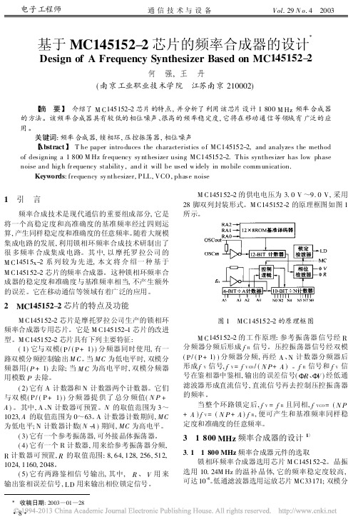
基于MC 145152-2芯片的频率合成器的设计XDesign of A Frequency Synthesizer Based on MC 145152-2何 强,王 丹(南京工业职业技术学院 江苏南京210002)【摘 要】 介绍了M C 145152-2芯片的特点,并分析了利用该芯片设计1800M Hz 频率合成器的方法。
该频率合成器具有较低的相位噪声、很高的频率稳定度,它将在移动通信等领域有广泛的应用。
关键词:频率合成器,锁相环,压控振荡器,相位噪声【Abstract 】 T he paper intro duces the characteristics o f MC145152-2,and analyzes the method of designing a 1800M Hz fr equency sy nthesizer using MC145152-2.This synthesizer has low phase noise and hig h fr equency stability ,and it will be used w idely in mo bile comm unication.Keywords :frequency sy nthesizer,PLL,VCO,phase noise1 引 言频率合成技术是现代通信的重要组成部分,它是将一个高稳定度和高准确度的基准频率经过四则运算,产生同样稳定度和准确度的任意频率。
随着大规模集成电路的发展,利用锁相环频率合成技术研制出了很多频率合成集成电路。
其中,以摩托罗拉公司的M C 14515x -2系列较为先进,本文将介绍一种基于M C145152-2芯片的频率合成器。
这种锁相环频率合成器的稳定度和准确度与基准频率相当,不产生额外的误差。
它在移动通信等领域有着广泛的应用。
2 MC 145152-2芯片的特点及功能M C145152-2芯片是摩托罗拉公司生产的锁相环频率合成器专用芯片。
CD4513
TRUTH TABLE
Inputs
Outputs
RBI LE BI LT D C B A RBO a b c d e f g Display
X X X 0 XXXX + 1 1 1 1 1 1 1 8
X X 0 1 X X X X + 0 0 0 0 0 0 0 Blank
1 0 1 1 0 0 0 0 1 0 0 0 0 0 0 0 Blank 0 0 1 1 0000 0 1111110 0
பைடு நூலகம்
VDD
Typ
Symbol Vdc
Min
Max
Min (Note 3) Max
Min
Max Unit
Output Voltage — Segment Outputs VOL
“0” Level
5.0
Vin = VDD or 0
10
15
−
0.05
−
−
0.05
−
−
0.05
−
Vdc
0
0.05
−
0.05
0
0.05
MC14513B
BCD−To−Seven Segment Latch/Decoder/Driver
CMOS MSI (Low−Power Complementary MOS)
The MC14513B BCD−to−seven segment latch/decoder/driver is constructed with complementary MOS (CMOS) enhancement mode devices and NPN bipolar output drivers in a single monolithic structure. The circuit provides the functions of a 4−bit storage latch, an 8421 BCD−to−seven segment decoder, and has output drive capability. Lamp test (LT), blanking (BI), and latch enable (LE) inputs are used to test the display, to turn−off or pulse modulate the brightness of the display, and to store a BCD code, respectively. The Ripple Blanking Input (RBI) and Ripple Blanking Output (RBO) can be used to suppress either leading or trailing zeroes. It can be used with seven−segment light emitting diodes (LED), incandescent, fluorescent, gas discharge, or liquid crystal readouts either directly or indirectly.
MC14553中文资料
X 1 1 0 X X X
X X X X
This device contains protection circuitry to guard against damage due to high static voltages or electric fields. However, precautions must be taken to avoid applications of any voltage higher than maximum rated voltages to this high–impedance circuit. For proper operation, Vin and Vout should be constrained to the range VSS (Vin or Vout) VDD. Unused inputs must always be tied to an appropriate logic voltage level (e.g., either VSS or VDD). Unused outputs must be left open.
MAXIMUM RATINGS* (Voltages Referenced to VSS)
Symbol VDD Parameter DC Supply Voltage Value Unit V V – 0.5 to + 18.0 Vin, Vout Iin Iout PD Tstg TL Input or Output Voltage (DC or Transient) Input Current (DC or Transient), per Pin Output Current (DC or Transient), per Pin Power Dissipation, per Package† Storage Temperature Lead Temperature (8–Second Soldering) – 0.5 to VDD + 0.5 ± 10 + 20 500 – 65 to + 150 260 mA mA mW
MC14541BDG中文资料
MC14541B
Programmable Timer
The MC14541B programmable timer consists of a 16−stage binary
counter, an integrated oscillator for use with an external capacitor and
MC14541BDTR2G
TSSOP−14*
MC14541BF MC14541BFG
SOEIAJ−14
SOEIAJ−14 (Pb−Free)
50 Units / Rail
MC14541BFEL MC14541BFELG
SOEIAJ−14
SOEIAJ−14 (Pb−Free)
2000 / Tape & Reel
15 – 16.3
−
– 13.2 – 26.33
mAdc
−
– 4.49
−
−
– 2.37
−
−
− 9.24
−5Leabharlann 01.93−1.56
3.12
10
4.96
−
4.0
8.0
15
19.3
−
15.6
31.2
−
1.09
− mAdc
−
2.8
−
−
10.9
−
15
−
± 0.1
− ± 0.00001 ± 0.1
−
± 1.0 mAdc
Features
• Available Outputs 28, 210, 213 or 216 • Increments on Positive Edge Clock Transitions • Built−in Low Power RC Oscillator (± 2% accuracy over temperature
默纳克HCB板选型手册 V2.1(最新版)
苏州默纳克控制技术有限公司Suzhou Monarch Control Technology Co.,Ltd 默纳克HCB板选型手册Ver 2.1目录序HCB板简表 (3)第一章无显示型 (4)1.1MCTC-HCB-B (4)第二章点阵显示型 (14)2.1MCTC-HCB-F (14)2.2MCTC-HCB-G1 (15)2.3MCTC-HCB-G2 (16)2.4MCTC-HCB-G4 (17)2.5MCTC-HCB-H (17)2.6MCTC-HCB-H1 (18)2.7MCTC-HCB-H2 (18)2.8MCTC-HCB-J1 (18)2.9MCTC-HCB-J2 (19)2.10MCTC-HCB-P1 (19)2.11MCTC-HCB-Q1 (20)2.12MCTC-HCB-Q2 (21)2.13MCTC-HCB-R1 (21)2.14MCTC-HCB-R2 (22)2.15MCTC-HCB-R4 (22)2.16MCTC-HCB-R5 (24)2.17MCTC-HCB-S3 (24)2.18MCTC-HCB-SL (24)2.19MCTC-HCB-Y1 (24)第三章普通液晶显示板 (24)3.1MCTC-HCB-D2 (24)3.2MCTC-HCB-K (24)3.3MCTC-HCB-M3 (24)3.4MCTC-HCB-M4 (24)3.5MCTC-HCB-U1 (24)3.6MCTC-HCB-U2 (24)3.7MCTC-HCB-V1 (24)3.8MCTC-HCB-Z1 (24)第四章 TFT液晶显示板 (24)4.1MCTC-HCB-T1 (24)4.2MCTC-HCB-T2 (24)4.3MCTC-HCB-T3 (24)第五章已停售型号 (24)友情提醒:此手册供选型使用,在确定型号后如需更加详细的各HCB板资料,请向默纳克公司索取。
序HCB板简表名称 特性 尺寸(mm)无显示外召MCTC-HCB-B 无显示外招 70*84*20点阵显示板MCTC-HCB-F 红色字体,横显 144*70*21MCTC-HCB-G1 大面积显示,红色字体,横竖显兼具157*65*22MCTC-HCB-G2 大面积显示,橙色字体,横竖显兼具157*65*22MCTC-HCB-G4 大面积显示,蓝色字体,横竖显兼具157*65*22MCTC-HCB-H 红色字体,竖显 144*70*21MCTC-HCB-H1 蓝色字体,竖显 144*70*21MCTC-HCB-H2 橙色字体,竖显 144*70*21MCTC-HCB-J1 红色字体,竖显 144*70*18MCTC-HCB-J2 橙色字体,竖显 144*70*18MCTC-HCB-P1 七段码显示板,红色字体 144*70*18MCTC-HCB-Q1 迷你点阵,红色字体 74*67*10MCTC-HCB-Q2 迷你点阵,橙色字体 74*67*10MCTC-HCB-R1超薄显示板,红色字体 144*70*10MCTC-HCB-R2超薄显示板,橙色字体 144*70*10MCTC-HCB-R4超薄显示板,红色字体 144*70*8.5MCTC-HCB-R5超薄显示板,红色字体 144*70*10MCTC-HCB-S3 白色字体(属HCB-H系列)144*70*21MCTC-HCB-SL 超长型显示板,红色字体245*55*15MCTC-HCB-Y1 点阵型并联专用显示板,橙色字体133*130*10普通液晶显示板MCTC-HCB-D2 超薄段码液晶,蓝底白字 144*70*10MCTC-HCB-K 单色液晶,蓝底白字 194*109*20MCTC-HCB-M3 段码液晶,黑底黄字 175*85*9MCTC-HCB-M4 段码液晶,黑底白字 175*85*9MCTC-HCB-U1 段码液晶,蓝底白字 144*80*17MCTC-HCB-U2 段码液晶,黑底白字 144*80*17MCTC-HCB-V1 段码液晶,蓝底白字 185*131*18MCTC-HCB-Z1 段码液晶并联专用显示板,蓝底白字135*129*16TFT液晶显示板MCTC-HCB-T1 4.3寸真彩液晶 145*85*18MCTC-HCB-T2 7寸真彩液晶 188*113*28MCTC-HCB-T3 9.7寸真彩液晶 250*194*32第一章 无显示型1.1 MCTC-HCB-B1.1.1 概述:¾ 整体尺寸:70mm*84mm*20mm¾ 6路开关量输入,4路继电器输出,6路集电极输出¾ 通过拨码设置,可以实现8种不同功能,满足多种场合的复杂需求1.1.2 实物及尺寸图CN189S52JP1JP3JP5JP2JP4JP6CN2K1K2K3K4S1A1A2AM B2B1BM C1C2C3C4C5C656.2mm62.5m m84.0m m70.2mmS2FUN4FUN3TEST FUN1FUN2IMPE F5F4F3F2F1F0图1-1-1 MCTC-HCB-B 实物图 图1-1-2 MCTC-HCB-B 尺寸图1.1.3 端子使用说明: A 拨码开关说明S11~5 楼层地址设定,范围0~63S1.1 F0 楼层选择 S1.2 F1 楼层选择 S1.3 F2 楼层选择 S1.4 F3 楼层选择 S1.5 F4 楼层选择 S1.6 F5楼层选择S21~5 功能选择等功能S2.1 IMPE MOD 总线终端匹配电阻设定S2.2 FUN2 功能选择 S2.3 FUN1 功能选择 S2.4 TEST 测试用 S2.5 FUN3 功能选择 S2.6 FUN4功能选择B 输入输出端子功能说明及接线指导:引脚定义端子功能1 2 3 4JP1 锁梯输入+24V+24V锁梯输入锁梯指示灯输出JP2 消防输入+24V+24V消防输入消防指示灯输出JP3 上行召唤按钮输入+24V+24V上行按钮输入按钮灯输出JP4 下行召唤按钮输入+24V+24V下行按钮输入按钮灯输出JP5 残障上行召唤按钮输入+24V+24V上行按钮输入按钮灯输出JP6 残障下行召唤按钮输入+24V+24V下行按钮输入按钮灯输出CN1 电源、通讯端子+24V MOD+MOD- COMCN2 继电器输出端子详见功能说明部分CN3 集电极输出端子详见功能说明部分附:输入端子下方PCB上白点对应的引脚为1脚,向另一侧依次为2、3、4脚。
MC12148中文资料

q
L 0.10 A1 B 0.25
M
C B
S
A
S
q
SD SUFFIX PLASTIC PACKAGE CASE 940-03 (SSOP–8) ISSUE B
8X
K REF 0.12 (0.005)
0.25 (0.010)
M
T U
S
V
S
N M
L/2 L
PIN 1 IDENT 1
NOTE: ESD data available upon request.
Symbol
VCC TA Tstg
Value
–0.5 to 7.0 –40 to 85 –65 to 150
Unit
Vdc °C °C
ELECTRICAL CHARACTERISTICS (VCC = 5.0 V; TA = –40 to 85°C, unless otherwise noted.)
MC12148D MC12148SD
© Motorola, Inc. 1997
元器件交易网
MC12148
MAXIMUM RATINGS Parameter
Power Supply Voltage, Pins 1, 7 Operating Temperature Range Storage Temperature Range
The MC12148 requires an external parallel tank circuit consisting of the inductor (L) and capacitor (C). A varactor diode may be incorporated into the tank circuit to provide a voltage variable input for the oscillator (VCO). This device may also be used in many other applications requiring a fixed frequency clock. The MC12148 is ideal in applications requiring a local oscillator. Systems include electronic test equipment and digital high–speed telecommunications. The MC12148 is based on the VCO circuit topology of the MC1648. The MC12148 has been realized utilizing Motorola’s MOSAIC III advanced bipolar process technology which results in a design which can operate at a much higher frequency than the MC1648 while utilizing half the current. Please consult with the MC1648 data sheet for additional background information. The ECL output circuitry of the MC12148 is not a traditional open emitter output structure and instead has an on–chip termination resistor with a nominal value of 500 ohms. This facilitates direct ac–coupling of the output signal into a transmission line. Because of this output configuration, an external pull–down resistor is not required to provide the output with a dc current path. This output is intended to drive one ECL load. If the user needs to fanout the signal, an ECL buffer such as the MC10EL16 Line Receiver/Driver should be used. NOTE: The MC12148 is NOT useable as a crystal oscillator.
申博COM1400

COM1400技术手册版本1.5盛博科技目 录第一章模块介绍 (1)1.1概述 (1)1.2 性能特点 (1)1.3 物理特性 (1)第二章硬件配置及安装 (3)2.1连接器功能及引脚定义 (3)2.1.1 连接器综述 (3)2.1.2 总线接口(J1) (4)2.2 安装 (6)第三章软件设置 (7)3.1 BIOS Setup的主画面 (7)3.1.1 Standard COMS Features(标准COMS参数设置) (7)3.1.2 Advanced BIOS Features(扩展BIOS特性设置) (11)3.1.3 Advanced Chipset Features(芯片组特性设置) (14)3.1.4 Integrated Peripherals(在板集成设备) (17)3.1.5 Power Management Setup(能源管理参数设置) (20)3.1.6 PnP/PCI Configurations(即插即用与PCI参数设置) (23)3.1.7 PC Health Status(电脑健康状态) (24)3.1.8 Frequency/V oltage Control(频率和电压控制) (24)3.1.9 Load Fail-Safe Defaults(载入最安全的缺省值) (25)3.1.10 Load Optimized Defaults(装入最优化的缺省值) (25)3.1.11 Set Supervisor Password(设置超级用户密码) (25)3.1.12 Set User Password(设置用户密码) (25)3.1.13 Save & Exit Setup(保存并退出设置程序) (25)3.1.14 Exit Without Saving(退出设置程序,不更新CMOS内容) (25)3.2 Watchdog (25)3.3 GPIO (28)附录A COM1400资源分配 (31)— i —图表目录图2-1. COM1400机械尺寸(单位:mm) (3)表2-1. 连接器功能 (4)表2-2. 总线接口(J1) (5)表2-3. 复用信号对应表 (6)图3-1. COM1400 BIOS Setup的主画面 (7)图3-2. 标准CMOS参数设置屏 (8)图3-3. IDE Primary Master 设置图 (9)图3-4. Advanced BIOS Features设置 (11)图3-5. Removable Device Priority设置 (12)图3-6. Hard Disk Boot Priority设置 (12)图3-7. Advanced Chipset Features设置 (15)图3-8. Integrated Peripherals设置 (17)图3-9. OnChip IDE Device设置图 (17)图3-10. Onboard Device设置 (18)图3-11. SuperIO Device设置 (19)图3-12. Power Management Setup设置 (21)图3-13. PnP/PCI Configurations设置 (23)图3-14. PC Health Status设置 (24)图3-15. Frequency/V oltage Control设置 (25)表A-1. 1M地址以下内存ROM空间分配 (31)表A-2. 中断资源分配 (31)表A-3. I/O地址空间分配 (32)表A-4. DMA通道分配 (33)— ii —第一章模块介绍1.1概述COM1400是一款采用新一代超低功耗Intel Pentium M / Intel Celeron M处理器的核心模块,提供使产品快速进入市场的解决方案。
mc1413中文资料

MC14015B
MC14015B Dual 4-Bit Static Shift RegisterThe MC14015B dual 4–bit static shift register is constructed with MOS P–channel and N–channel enhancement mode devices in a single monolithic structure. It consists of two identical, independent 4–state serial–input/parallel–output registers. Each register has independent Clock and Reset inputs with a single serial Data input.The register states are type D master–slave flip–flops. Data is shifted from one stage to the next during the positive–going clock transition.Each register can be cleared when a high level is applied on the Reset line. These complementary MOS shift registers find primary use in buffer storage and serial–to–parallel conversion where low power dissipation and/or noise immunity is desired.•Diode Protection on All Inputs•Supply V oltage Range = 3.0 Vdc to 18 Vdc •Logic Edge–Clocked Flip–Flop Design —Logic state is retained indefinitely with clock level either high or low;information is transferred to the output only on the positive going edge of the clock pulse.•Capable of Driving Two Low–power TTL Loads or One Low–power Schottky TTL Load Over the Rated Temperature Range.MAXIMUM RATINGS (Voltages Referenced to V) (Note 2.)may occur.3.Temperature Derating:Plastic “P and D/DW” Packages: – 7.0 mW/_C From 65_C To 125_C This device contains protection circuitry to guard against damage due to high static voltages or electric fields. However, precautions must be taken to avoid applications of any voltage higher than maximum rated voltages to this high–impedance circuit. For proper operation, V in and V out should be constrained to the range V SS v (V in or V out ) v V DD .Unused inputs must always be tied to an appropriate logic voltage level (e.g.,either V SS or V DD ). Unused outputs must be left open.1.For ordering information on the EIAJ version of the SOIC packages, please contact your local ON Semiconductor representative.TRUTH TABLEX = Don’t CareQ n = Q0, Q1, Q2, or Q3, as applicable.Q n–1 = Output of prior stage.BLOCK DIAGRAM14115697543101312112V DD = PIN 16V SS = PIN 8PIN ASSIGNMENTQ1B Q0B R B D B V DD C AQ3A Q2B Q1A Q2A Q3B C B V SSD A R A Q0A5.The formulas given are for the typical characteristics only at 25_C.6.To calculate total supply current at loads other than 50 pF:I T(C L) = I T(50 pF) + (C L – 50) Vfkwhere: I T is in µA (per package), C L in pF, V = (V DD – V SS) in volts, f in kHz is input frequency, and k = 0.002.8.Data labelled “Typ” is not to be used for design purposes but is intended as an indication of the IC’s potential performance.Figure 1. Power Dissipation Test Circuit and WaveformFigure 2. Switching Test Circuit and WaveformsC LDD DD t TLHTHLt WL = t WH = 50% Duty Cycle tTLH = t THL ≤ 20 nsFigure 3. Setup and Hold Time Test Circuit and WaveformsC LCLOCK INPUTDATA INPUTDD DDLOGIC DIAGRAMSSINGLE BIT14115697PDIP–16P SUFFIX PLASTIC DIP PACKAGENOTES:1.DIMENSIONING AND TOLERANCING PER ANSIY14.5M, 1982.2.CONTROLLING DIMENSION: INCH.3.DIMENSION L TO CENTER OF LEADS WHENFORMED PARALLEL.4.DIMENSION B DOES NOT INCLUDE MOLD FLASH.5.ROUNDED CORNERS OPTIONAL.MDIM MIN MAX MIN MAXMILLIMETERSINCHESA0.7400.77018.8019.55B0.2500.270 6.35 6.85C0.1450.175 3.69 4.44D0.0150.0210.390.53F0.0400.70 1.02 1.77G0.100 BSC 2.54 BSCH0.050 BSC 1.27 BSCJ0.0080.0150.210.38K0.1100.130 2.80 3.30L0.2950.3057.507.74M0 10 0 10S0.0200.0400.51 1.01____SOIC–16D SUFFIXPLASTIC SOIC PACKAGECASE 751B–05NOTES:1.DIMENSIONING AND TOLERANCING PER ANSI Y14.5M, 1982.2.CONTROLLING DIMENSION: MILLIMETER.3.DIMENSIONS A AND B DO NOT INCLUDE MOLD PROTRUSION.4.MAXIMUM MOLD PROTRUSION 0.15 (0.006)PER SIDE.5.DIMENSION D DOES NOT INCLUDE DAMBAR PROTRUSION. ALLOWABLE DAMBARPROTRUSION SHALL BE 0.127 (0.005) TOTAL IN EXCESS OF THE D DIMENSION AT MAXIMUM MATERIAL CONDITION.SBM0.25 (0.010)AST DIM MIN MAX MIN MAX INCHESMILLIMETERS A 9.8010.000.3860.393B 3.80 4.000.1500.157C 1.35 1.750.0540.068D 0.350.490.0140.019F 0.40 1.250.0160.049G 1.27 BSC 0.050 BSC J 0.190.250.0080.009K 0.100.250.0040.009M 0 7 0 7 P 5.80 6.200.2290.244R0.250.500.0100.019____TSSOP–16DT SUFFIXPLASTIC TSSOP PACKAGECASE 948F–01ISSUE ODIM MIN MAX MIN MAX INCHESMILLIMETERS A 4.90 5.100.1930.200B 4.30 4.500.1690.177C --- 1.20---0.047D 0.050.150.0020.006F 0.500.750.0200.030G 0.65 BSC 0.026 BSC H 0.180.280.0070.011J 0.090.200.0040.008J10.090.160.0040.006K 0.190.300.0070.012K10.190.250.0070.010L 6.40 BSC 0.252 BSC M0 8 0 8 DIMENSIONING AND TOLERANCING PER ANSIY14.5M, 1982.CONTROLLING DIMENSION: MILLIMETER.DIMENSION A DOES NOT INCLUDE MOLDFLASH. PROTRUSIONS OR GATE BURRS. MOLD FLASH OR GATE BURRS SHALL NOT EXCEED 0.15(0.006) PER SIDE.DIMENSION B DOES NOT INCLUDE INTERLEADFLASH OR PROTRUSION. INTERLEAD FLASH OR PROTRUSION SHALL NOT EXCEED 0.25 (0.010) PER SIDE.DIMENSION K DOES NOT INCLUDE DAMBARPROTRUSION. ALLOWABLE DAMBARPROTRUSION SHALL BE 0.08 (0.003) TOTAL IN EXCESS OF THE K DIMENSION AT MAXIMUM MATERIAL CONDITION.TERMINAL NUMBERS ARE SHOWN FORREFERENCE ONLY.DIMENSION A AND B ARE TO BE DETERMINEDAT DATUM PLANE -W-.____16X REF11PACKAGE DIMENSIONSNOTES:ąă1.DIMENSIONING AND TOLERANCING PER ANSIY14.5M, 1982.SOEIAJ–16F SUFFIXPLASTIC EIAJ SOIC PACKAGECASE 966–01ISSUE OON Semiconductor and are trademarks of Semiconductor Components Industries, LLC (SCILLC). SCILLC reserves the right to make changes without further notice to any products herein. SCILLC makes no warranty, representation or guarantee regarding the suitability of its products for any particular purpose, nor does SCILLC assume any liability arising out of the application or use of any product or circuit, and specifically disclaims any and all liability, including without limitation special, consequential or incidental damages. “Typical” parameters which may be provided in SCILLC data sheets and/or specifications can and do vary in different applications and actual performance may vary over time. All operating parameters, including “Typicals” must be validated for each customer application by customer’s technical experts. SCILLC does not convey any license under its patent rights nor the rights of others.SCILLC products are not designed, intended, or authorized for use as components in systems intended for surgical implant into the body, or other applications intended to support or sustain life, or for any other application in which the failure of the SCILLC product could create a situation where personal injury or death may occur. Should Buyer purchase or use SCILLC products for any such unintended or unauthorized application, Buyer shall indemnify and hold SCILLC and its officers, employees, subsidiaries, affiliates, and distributors harmless against all claims, costs, damages, and expenses, and reasonable attorney fees arising out of, directly or indirectly, any claim of personal injury or death associated with such unintended or unauthorized use, even if such claim alleges that SCILLC was negligent regarding the design or manufacture of the part. SCILLC is an Equal Opportunity/Affirmative Action Employer. PUBLICATION ORDERING INFORMATIONCENTRAL/SOUTH AMERICA:Spanish Phone:303–308–7143 (Mon–Fri 8:00am to 5:00pm MST)Email:ONlit–spanish@ASIA/PACIFIC: LDC for ON Semiconductor – Asia SupportPhone:303–675–2121 (Tue–Fri 9:00am to 1:00pm, Hong Kong Time)Toll Free from Hong Kong & Singapore:001–800–4422–3781Email: ONlit–asia@JAPAN: ON Semiconductor, Japan Customer Focus Center4–32–1 Nishi–Gotanda, Shinagawa–ku, Tokyo, Japan 141–0031Phone: 81–3–5740–2745Email: r14525@。
MC14513B中文资料
ON Semiconductor and are trademarks of Semiconductor Components Industries, LLC (SCILLC). SCILLC reserves the right to make changes without further notice to any products herein. SCILLC makes no warranty, representation or guarantee regarding the suitability of its products for any particular purpose, nor does SCILLC assume any liability arising out of the application or use of any product or circuit, and specifically disclaims any and all liability, including without limitation special, consequential or incidental damages. “Typical” parameters which may be provided in SCILLC data sheets and/or specifications can and do vary in different applications and actual performance may vary over time. All operating parameters, including “Typicals” must be validated for each customer application by customer’s technical experts. SCILLC does not convey any license under its patent rights nor the rights of others.SCILLC products are not designed, intended, or authorized for use as components in systems intended for surgical implant into the body, or other applications intended to support or sustain life, or for any other application in which the failure of the SCILLC product could create a situation where personal injury or death may occur. Should Buyer purchase or use SCILLC products for any such unintended or unauthorized application, Buyer shall indemnify and hold SCILLC and its officers, employees, subsidiaries, affiliates, and distributors harmless against all claims, costs, damages, and expenses, and reasonable attorney fees arising out of, directly or indirectly, any claim of personal injury or death associated with such unintended or unauthorized use, even if such claim alleges that SCILLC was negligent regarding the design or manufacture of the part. SCILLC is an Equal Opportunity/Affirmative Action Employer. PUBLICATION ORDERING INFORMATIONCENTRAL/SOUTH AMERICA:Spanish Phone:303–308–7143 (Mon–Fri 8:00am to 5:00pm MST)Email:ONlit–spanish@ASIA/PACIFIC: LDC for ON Semiconductor – Asia SupportPhone:303–675–2121 (Tue–Fri 9:00am to 1:00pm, Hong Kong Time)Toll Free from Hong Kong & Singapore:001–800–4422–3781Email: ONlit–asia@JAPAN: ON Semiconductor, Japan Customer Focus Center4–32–1 Nishi–Gotanda, Shinagawa–ku, Tokyo, Japan 141–8549Phone: 81–3–5740–2745Email: r14525@。
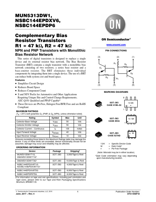
SCI 数字透视器:Bias 电阻透视器(BRT)数据手册说明书
MUN5313DW1,NSBC144EPDXV6,NSBC144EPDP6Complementary Bias Resistor Transistors R1 = 47 k W , R2 = 47 k WNPN and PNP Transistors with Monolithic Bias Resistor NetworkThis series of digital transistors is designed to replace a single device and its external resistor bias network. The Bias Resistor Transistor (BRT) contains a single transistor with a monolithic bias network consisting of two resistors; a series base resistor and a base-emitter resistor. The BRT eliminates these individual components by integrating them into a single device. The use of a BRT can reduce both system cost and board space.Features•Simplifies Circuit Design •Reduces Board Space•Reduces Component Count•S and NSV Prefix for Automotive and Other Applications Requiring Unique Site and Control Change Requirements;AEC-Q101 Qualified and PPAP Capable*•These Devices are Pb-Free, Halogen Free/BFR Free and are RoHS CompliantMAXIMUM RATINGS(T A = 25°C both polarities Q 1 (PNP) & Q 2 (NPN), unless otherwise noted)RatingSymbol Max Unit Collector-Base Voltage V CBO 50Vdc Collector-Emitter Voltage V CEO 50Vdc Collector Current − Continuous I C 100mAdc Input Forward Voltage V IN(fwd)40VdcInput Reverse VoltageV IN(rev)10Vdc Stresses exceeding those listed in the Maximum Ratings table may damage the device. If any of these limits are exceeded, device functionality should not be assumed, damage may occur and reliability may be affected.ORDERING INFORMATIONDevicePackage Shipping †MUN5313DW1T1G,SMUN5313DW1T1G*SOT−3633,000/T ape & Reel SMUN5313DW1T3G*SOT−36310,000/T ape & Reel NSBC144EPDXV6T1G NSVBC144EPDXV6T1G*SOT−5634,000/T ape & Reel NSBC144EPDXV6T5G SOT−5638,000/T ape & Reel NSBC144EPDP6T5GSOT−9638,000/T ape & Reel†For information on tape and reel specifications, including part orientation andtape sizes, please refer to our Tape and Reel Packaging Specifications Brochure, BRD8011/D. MARKING DIAGRAMSPIN CONNECTIONS13/K =Specific Device Code M =Date Code*G =Pb-Free Package(Note: Microdot may be in either location)*Date Code orientation may vary depending upon manufacturing location.SOT−363CASE 419B−02SOT−563CASE 463A(1)(2)(3)(6)(5)(4)SOT−963CASE 527ADM1K13 M G G1613 M G 1THERMAL CHARACTERISTICSCharacteristic Symbol Max Unit MUN5313DW1 (SOT−363) ONE JUNCTION HEATEDTotal Device DissipationT A = 25°C(Note1)(Note2)Derate above 25°C(Note1)(Note2)P D1872561.52.0mWmW/°CThermal Resistance,(Note1) Junction to Ambient(Note2)R q JA670490°C/WMUN5313DW1 (SOT−363) BOTH JUNCTION HEATED (Note3)Total Device DissipationT A = 25°C(Note1)(Note2)Derate above 25°C(Note1)(Note2)P D2503852.03.0mWmW/°CThermal Resistance,Junction to Ambient(Note1)(Note2)R q JA493325°C/WThermal Resistance, Junction to Lead(Note1)(Note2)R q JL188208°C/WJunction and Storage Temperature Range T J, T stg−55 to +150°C NSBC144EPDXV6 (SOT−563) ONE JUNCTION HEATEDTotal Device DissipationT A = 25°C(Note1)Derate above 25°C(Note1)P D3572.9mWmW/°CThermal Resistance,Junction to Ambient(Note1)R q JA350°C/WNSBC144EPDXV6 (SOT−563) BOTH JUNCTION HEATED (Note3)Total Device DissipationT A = 25°C(Note1)Derate above 25°C(Note1)P D5004.0mWmW/°CThermal Resistance,Junction to Ambient(Note1)R q JA250°C/WJunction and Storage Temperature Range T J, T stg−55 to +150°C NSBC144EPDP6 (SOT−963) ONE JUNCTION HEATEDTotal Device DissipationT A = 25°C(Note4)(Note5)Derate above 25°C(Note4)(Note5)P D2312691.92.2MWmW/°CThermal Resistance,Junction to Ambient(Note4)(Note5)R q JA540464°C/WNSBC144EPDP6 (SOT−963) BOTH JUNCTION HEATED (Note3)Total Device DissipationT A = 25°C(Note4)(Note5)Derate above 25°C(Note4)(Note5)P D3394082.73.3MWmW/°CThermal Resistance,Junction to Ambient(Note4)(Note5)R q JA369306°C/WJunction and Storage Temperature Range T J, T stg−55 to +150°C1.FR−4 @ Minimum Pad.2.FR−*****×1.0 Inch Pad.3.Both junction heated values assume total power is sum of two equally powered channels.4.FR−4 @ 100mm2, 1 oz. copper traces, still air.5.FR−4 @ 500mm2, 1 oz. copper traces, still air.ELECTRICAL CHARACTERISTICS (T A=25°C both polarities Q1 (PNP) & Q2 (NPN), unless otherwise noted)Characteristic Symbol Min Typ Max Unit OFF CHARACTERISTICSCollector-Base Cutoff Current (V CB=50V, I E=0)I CBO−−100nAdcCollector-Emitter Cutoff Current (V CE=50V, I B=0)I CEO−−500nAdcEmitter-Base Cutoff Current (V EB=6.0V, I C=0)I EBO−−0.1mAdcCollector-Base Breakdown Voltage (I C=10m A, I E=0)V(BR)CBO50−−VdcCollector-Emitter Breakdown Voltage (Note6) (I C=2.0mA, I B=0)V(BR)CEO50−−VdcON CHARACTERISTICSDC Current Gain (Note6) (I C=5.0mA, V CE=10V)h FE80140−Collector-Emitter Saturation Voltage (Note6) (I C=10mA, I B=0.3mA)V CE(sat)−−0.25VInput Voltage (Off)(V CE=5.0V, I C=100m A) (NPN) (V CE=5.0V, I C=100m A) (PNP)V i(off)−−1.21.2−−VdcInput Voltage (On)(V CE=0.2V, I C=3.0mA) (NPN)(V CE=0.2V, I C=3.0mA) (PNP)V i(on)−−1.92.0−−VdcOutput Voltage (On)(V CC=5.0V, V B=3.5V, R L=1.0k W)V OL−−0.2VdcOutput Voltage (Off)(V CC=5.0V, V B=0.5V, R L=1.0k W)V OH4.9−−Vdc Input Resistor R132.94761.1k W Resistor Ratio R1/R20.8 1.0 1.26.Pulsed Condition: Pulse Width=300ms, Duty Cycle ≤2%.Figure 1. Derating CurveAMBIENT TEMPERATURE (°C)PD,POWERDISSIPATION(mW)(1) SOT−363; 1.0×1.0 Inch Pad(2) SOT−563; Minimum Pad(3) SOT−963; 100mm2, 1 oz. Copper TraceFigure 2. V CE(sat) vs. I C246810V in , INPUT VOLTAGE (V)Figure 3. DC Current GainFigure 4. Output Capacitance I C , COLLECTOR CURRENT (mA)Figure 5. Output Current vs. Input VoltageI C , COLLECTOR CURRENT (mA)3.22.81.20.80.40V R , REVERSE VOLTAGE (V)Figure 6. Input Voltage vs. Output CurrentI C , COLLECTOR CURRENT (mA)V C E (s a t ), C O L L E C T O R −E M I T T E R V O L T A G E (V )h F E , D C C U R R E N T G A I N 1.62.02.4C o b , O U T P U T C A P A C I T A N C E (p F )I C , C O L L E C T O R C U R R E N T (m A )V i n , I N P U T V O L T A G E (V )Figure 7. V CE(sat) vs. I C1001010.1I C , COLLECTOR CURRENT (mA)Figure 8. DC Current GainFigure 9. Output Capacitance 1001010.10.010.001V in , INPUT VOLTAGE (V)Figure 10. Output Current vs. Input Voltage100010010I C , COLLECTOR CURRENT (mA)Figure 11. Input Voltage vs. Output CurrentI C , COLLECTOR CURRENT (mA)10.10.01V R , REVERSE VOLTAGE (V)C o b , O U T P U T C A P A C I T A N C E (p F )V i n , I N P U T V O L T A G E (V )V C E (s a t ), C O L L E C T O R −E M I T T E R V O L T A G E (V )I C , C O L L E C T O R C U R R E N T (m A )h F E , C U R R E N T G A I NFigure 12. V CE(sat) vs. I CI C , COLLECTOR CURRENT (mA)10010.1Figure 13. DC Current GainFigure 14. Output Capacitance I C , COLLECTOR CURRENT (mA)10001001I C , COLLECTOR CURRENT (mA)Figure 15. Output Current vs. Input Voltage1001010.10.001V in , INPUT VOLTAGE (V)Figure 16. Input Voltage vs. Output Current0.41.20V R , REVERSE VOLTAGE (V)V C E (s a t ), C O L L E C T O R −E M I T T E R V O L T A G E (V )h F E , D C C U R R E N T G A I N 0.81.62.02.4C o b , O U T P U T C A P A C I T A N C E (p F )I C , C O L L E C T O R C U R R E N T (m A )V i n , I N P U T V O L T A G E (V )10100.01Figure 17. V CE(sat) vs. I CFigure 18. DC Current GainI C , COLLECTOR CURRENT (mA)I C , COLLECTOR CURRENT (mA)0.010.11Figure 19. Output CapacitanceFigure 20. Output Current vs. Input VoltageV R , REVERSE VOLTAGE (V)V in , INPUT VOLTAGE (V)Figure 21. Input Voltage vs. Output CurrentI C , COLLECTOR CURRENT (mA)V C E (s a t ), C O L L E C T O R −E M I T T E R V O L T A G E (V )h F E , D C C U R R E N T G A I N C o b , O U T P U T C A P A C I T A N C E (p F )I C , C O L L E C T O R C U R R E N T (m A )V i n , I N P U T V O L T A G E (V )SC−88/SC70−6/SOT−363CASE 419B−02ISSUE YNOTES:1.DIMENSIONING AND TOLERANCING PER ASME Y14.5M, 1994.2.CONTROLLING DIMENSION: MILLIMETERS.3.DIMENSIONS D AND E1 DO NOT INCLUDE MOLD FLASH,PROTRUSIONS, OR GATE BURRS. MOLD FLASH, PROTRU-SIONS, OR GATE BURRS SHALL NOT EXCEED 0.20 PER END.4.DIMENSIONS D AND E1 AT THE OUTERMOST EXTREMES OF THE PLASTIC BODY AND DATUM H.5.DATUMS A AND B ARE DETERMINED AT DATUM H.6.DIMENSIONS b AND c APPLY TO THE FLAT SECTION OF THE LEAD BETWEEN 0.08 AND 0.15 FROM THE TIP .7.DIMENSION b DOES NOT INCLUDE DAMBAR PROTRUSION.ALLOWABLE DAMBAR PROTRUSION SHALL BE 0.08 TOTAL IN EXCESS OF DIMENSION b AT MAXIMUM MATERIAL CONDI-TION. THE DAMBAR CANNOT BE LOCATED ON THE LOWER RADIUS OF THE FOOT.DIM MIN NOM MAX MILLIMETERS A −−−−−− 1.10A10.00−−−0.10dddb 0.150.200.25C 0.080.150.22D 1.80 2.00 2.20−−−−−−0.0430.000−−−0.0040.0060.0080.0100.0030.0060.0090.0700.0780.086MIN NOM MAX INCHES0.100.004E1 1.15 1.25 1.35e 0.65 BSC L 0.260.360.462.00 2.10 2.200.0450.0490.0530.026 BSC0.0100.0140.0180.0780.0820.086*For additional information on our Pb−Free strategy and soldering details, please download the ON Semiconductor Soldering and Mounting Techniques Reference Manual, SOLDERRM/D.SOLDERING FOOTPRINT*DIMENSIONS: MILLIMETERS0.306XRECOMMENDEDSIDE VIEWEND VIEWPLANEDETAIL AE A20.700.90 1.000.0270.0350.039L20.15 BSC 0.006 BSC aaa 0.150.006bbb 0.300.012ccc 0.100.0046XH EDIMMIN NOM MAX MILLIMETERS A 0.500.550.60b 0.170.220.27C D 1.50 1.60 1.70E 1.10 1.20 1.30e 0.5 BSC L 0.100.200.301.50 1.60 1.700.0200.0210.0230.0070.0090.0110.0590.0620.0660.0430.0470.0510.02 BSC0.0040.0080.0120.0590.0620.066MIN NOM MAX INCHESSOT−563, 6 LEADCASE 463A ISSUE GNOTES:1.DIMENSIONING AND TOLERANCING PER ANSI Y14.5M, 1982.2.CONTROLLING DIMENSION: MILLIMETERS3.MAXIMUM LEAD THICKNESS INCLUDES LEAD FINISH THICKNESS. MINIMUM LEAD THICKNESS IS THE MINIMUM THICKNESS OF BASE MATERIAL.ǒmm inchesǓSCALE 20:1*For additional information on our Pb-Free strategy and solderingdetails, please download the ON Semiconductor Soldering and Mounting Techniques Reference Manual, SOLDERRM/D.SOLDERING FOOTPRINT*0.080.120.180.0030.0050.007SOT−963CASE 527AD ISSUE EDIM MIN NOM MAX MILLIMETERS A 0.340.370.40b 0.100.150.20C 0.070.120.17D 0.95 1.00 1.05E 0.750.800.85e 0.35 BSC 0.95 1.00 1.05H E ANOTES:1.DIMENSIONING AND TOLERANCING PER ASME Y14.5M, 1994.2.CONTROLLING DIMENSION: MILLIMETERS3.MAXIMUM LEAD THICKNESS INCLUDES LEAD FINISH THICKNESS. MINIMUM LEADTHICKNESS IS THE MINIMUM THICKNESS OF BASE MATERIAL.4.DIMENSIONS D AND E DO NOT INCLUDE MOLD FLASH, PROTRUSIONS, OR GATE BURRS.TOP VIEW SIDE VIEWDIMENSIONS: MILLIMETERSRECOMMENDEDMOUNTING FOOTPRINT*L 0.19 REF L20.050.100.156X *For additional information on our Pb-Free strategy and soldering details, please download the ON Semiconductor Soldering and Mounting Techniques Reference Manual, SOLDERRM/D.ON Semiconductor and are trademarks of Semiconductor Components Industries, LLC dba ON Semiconductor or its subsidiaries in the United States and/or other countries.ON Semiconductor owns the rights to a number of patents, trademarks, copyrights, trade secrets, and other intellectual property. A listing of ON Semiconductor’s product/patent PUBLICATION ORDERING INFORMATION。
用MC14541B制作可编程序定时器
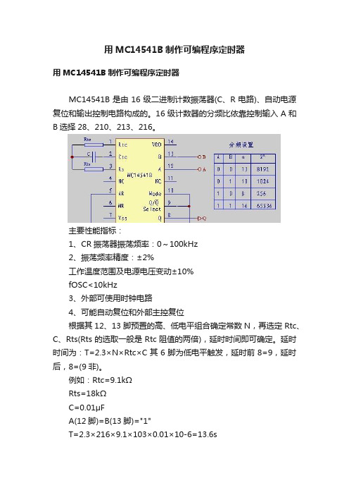
用MC14541B制作可编程序定时器
用MC14541B制作可编程序定时器
MC14541B是由16级二进制计数振荡器(C、R电路)、自动电源复位和输出控制电路构成的。
16级计数器的分频比依靠控制输入A和B选择28、210、213、216。
主要性能指标:
1、CR振荡器振荡频率:0~100kHz
2、振荡频率精度:±2%
工作温度范围及电源电压变动±10%
fOSC<10kHz
3、外部可使用时钟电路
4、可能自动复位和外部主控复位
根据其12、13脚预置的高、低电平组合确定常数N,再选定Rtc、C、Rts(Rts的选取一般是Rtc阻值的两倍),延时时间即可确定。
延时时间为:T=2.3×N×Rtc×C其6脚为低电平触发,延时前8=9,延时后,8=(9非)。
例如:Rtc=9.1kΩ
Rts=18kΩ
C=0.01μF
A(12脚)=B(13脚)="1"
T=2.3×216×9.1×103×0.01×10-6=13.6s。
基于MC数字电压表的设计

基于MC数字电压表的设计作者: 日期:题目一数子式电压表功能分析A/D转换及数字显示部分将输入电压转化为数字量,并输出显示。
这部分主要由以下几部分构成:3位半A/D转换单元电路(MC14433是美国Motorola公司推出的单片3 1/2位A/D转换器,其中集成了双积分式A/D转换器所有的CMOS模拟电路和数字电路。
具有外接元件少,输入阻抗高,功耗低,电源电压范围宽,精度高等特点,并且具有自动校零和自动极性转换功能,只要外接少量的阻容件即可构成一个完整的A/D转换器1.精度:读数的±0.05%±1字2.模拟电压输入量程:1.999V和K14433 11 农232221201916171«151413199.9mV两档3.转换速率:2-25次/s 4.输入阻抗:大于1000MD 6.功耗:8mW (±5V电源电压时,典型值)MC14433最主要的用途是数字电压表,数字温度计等各类数字化仪表及计算机数据采集系统的A/D转换接口。
312047 K14433的書朋枫12MC14433的引脚说明:[1]. Pinl(VAG)—模拟地,为高阻输入端,被测电压和基准电压的接入地。
[2] . Pin2(VR)—基准电压,此引脚为外接基准电压的输入端。
MC14433只要一个正基准电压即可测量正、负极性 的电压。
此外,VR 端只要加上一个大于5个时钟周期的负脉冲(VR),就能够复位为至转换周期的起始点。
[3] . Pin3(Vx)—被测电压的输入端,MC14433属于双积分型A/D 转换器,因而被测电压与基准电压有以下关系: 输出读数二醫X ⑷船因此,满量程的Vx=VR 。
当满量程选为1.999V ,VR 可取2.000V ,而当满量程为199.9mV 时,VR 取200.0mV , 在实际的应用电路中,根据需要,VR 值可在200mV —2.000V 之间选取。
[4] . Pin4-Pin6(R1/C1 ,C1)—外接积分元件端。
- 1、下载文档前请自行甄别文档内容的完整性,平台不提供额外的编辑、内容补充、找答案等附加服务。
- 2、"仅部分预览"的文档,不可在线预览部分如存在完整性等问题,可反馈申请退款(可完整预览的文档不适用该条件!)。
- 3、如文档侵犯您的权益,请联系客服反馈,我们会尽快为您处理(人工客服工作时间:9:00-18:30)。
ON Semiconductor and are trademarks of Semiconductor Components Industries, LLC (SCILLC). SCILLC reserves the right to make changes without further notice to any products herein. SCILLC makes no warranty, representation or guarantee regarding the suitability of its products for any particular purpose, nor does SCILLC assume any liability arising out of the application or use of any product or circuit, and specifically disclaims any and all liability, including without limitation special, consequential or incidental damages. “Typical” parameters which may be provided in SCILLC data sheets and/or specifications can and do vary in different applications and actual performance may vary over time. All operating parameters, including “Typicals” must be validated for each customer application by customer’s technical experts. SCILLC does not convey any license under its patent rights nor the rights of others.
SCILLC products are not designed, intended, or authorized for use as components in systems intended for surgical implant into the body, or other applications intended to support or sustain life, or for any other application in which the failure of the SCILLC product could create a situation where personal injury or death may occur. Should Buyer purchase or use SCILLC products for any such unintended or unauthorized application, Buyer shall indemnify and hold SCILLC and its officers, employees, subsidiaries, affiliates, and distributors harmless against all claims, costs, damages, and expenses, and reasonable attorney fees arising out of, directly or indirectly, any claim of personal injury or death associated with such unintended or unauthorized use, even if such claim alleges that SCILLC was negligent regarding the design or manufacture of the part. SCILLC is an Equal Opportunity/Affirmative Action Employer. PUBLICATION ORDERING INFORMATION
CENTRAL/SOUTH AMERICA:
Spanish Phone:303–308–7143 (Mon–Fri 8:00am to 5:00pm MST)
Email:ONlit–spanish@
ASIA/PACIFIC: LDC for ON Semiconductor – Asia Support
Phone:303–675–2121 (Tue–Fri 9:00am to 1:00pm, Hong Kong Time)
Toll Free from Hong Kong & Singapore:
001–800–4422–3781
Email: ONlit–asia@
JAPAN: ON Semiconductor, Japan Customer Focus Center
4–32–1 Nishi–Gotanda, Shinagawa–ku, Tokyo, Japan 141–8549
Phone: 81–3–5740–2745
Email: r14525@。