5962F0253502VYC中文资料
2N5962资料
VCE( sat) VBE( on)
Collector-Emitter Saturation Voltage Base-Emitter On Voltage
1400 0.2 0.7
V V
SMALL SIGNAL CHARACTERISTICS
Ccb Ceb hfe Collector-Base Capacitance Emitter-Base Capacitance Small-Signal Current Gain VCB = 5.0 V VEB = 0.5 V IC = 10 mA, VCE = 5.0 V, f = 1.0 kHz IC = 10 mA, VCE = 5.0 V, f = 100 MHz VCE = 5.0 V, IC = 10 µA, RS = 10 kΩ, f = 1.0 kHz, BW = 400 Hz VCE = 5.0 V, IC = 100 µA, RS = 1.0 kΩ, f = 1.0 kHz, BW = 400 Hz VCE = 5.0 V, IC = 100 µA, RS = 10 kΩ, f = 1.0 kHz, BW = 400 Hz VCE = 5.0 V, IC = 100 µA, RS = 100 kΩ, f = 1.0 kHz, BW = 400 Hz VCE = 5.0 V, IC = 10 µA, RS = 10 kΩ, f = 10 Hz -10 kHz BW = 15.7 kHz 600 1.0 4.0 6.0 200 pF pF
NF
Noise Figure
3.0
dB
6.0
dB
4.0
dB
8.0
dB
3.0
dB
*Pulse Test: Pulse Width ≤ 300 µs, Duty Cycle ≤ 2.0%
5962-8951105VEA中文资料
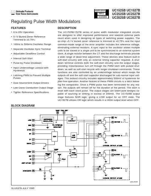
UC1525B UC1527B UC2525B UC2527B UC3525B UC3527BDESCRIPTIONThe UC1525B/1527B series of pulse width modulator integrated circuits are designed to offer improved performance and lowered external parts count when used in designing all types of switching power supplies.The on-chip +5.1V buried zener reference is trimmed to ±0.75%and the input common-mode range of the error amplifier includes the reference voltage,eliminating external resistors.A sync input to the oscillator allows multiple units to be slaved or a single unit to be synchronized to an external system clock.A single resistor between the CT and the discharge terminals provide a wide range of dead time adjustment.These devices also feature built-in soft-start circuitry with only an external timing capacitor required.A shut-down terminal controls both the soft-start circuitry and the output stages,providing instantaneous turn off through the PWM latch with pulsed shut-down,as well as soft-start recycle with longer shutdown commands.These functions are also controlled by an undervoltage lockout which keeps the outputs off and the soft-start capacitor discharged for sub-normal input volt-ages.This lockout circuitry includes approximately 500mV of hysteresis for jitter-free operation.Another feature of these PWM circuits is a latch follow-ing the comparator.Once a PWM pulse has been terminated for any rea-son,the outputs will remain off for the duration of the period.The latch is reset with each clock pulse.The output stages are totem-pole designs ca-pable of sourcing or sinking in excess of 200mA.The UC1525B output stage features NOR logic,giving a LOW output for an OFF state.The UC1527B utilizes OR logic which results in a HIGH output level when OFF.Regulating Pulse Width ModulatorsFEATURES•8to 35V Operation•5.1V Buried Zener Reference Trimmed to ±0.75%•100Hz to 500kHz Oscillator Range •Separate Oscillator Sync Terminal •Adjustable Deadtime Control •Internal Soft-Start •Pulse-by-Pulse Shutdown •Input Undervoltage Lockout with Hysteresis•Latching PWM to Prevent Multiple Pulses•Dual Source/Sink Output Drivers •Low Cross Conduction Output Stage •Tighter Reference SpecificationsBLOCK DIAGRAMABSOLUTE MAXIMUM RATINGSSupply Voltage,(+VIN)...........................+40V Collector Supply Voltage (VC)......................+40V Logic Inputs ............................–0.3V to +5.5V Analog Inputs.............................–0.3V to VIN Output Current,Source or Sink ...................500mA Reference Output Current ........................50mA Oscillator Charging Current ........................5mA Power Dissipation at T A =+25°C.................1000mW Power Dissipation at T C =+25°C ................2000mW Operating Junction Temperature ..........–55°C to +150°C Storage Temperature Range .............–65°C to +150°C Lead Temperature (Soldering,10sec.).............+300°C All currents are positive into,negative out of the specified ter-minal.Consult Packaging Section of Databook for thermal limi-tations and considerations of packages.RECOMMENDED OPERATING CONDITIONS (Note 1)Input Voltage (+VIN).......................+8V to +35V Collector Supply Voltage (VC)..............+4.5V to +35V Sink/Source Load Current (steady state)........0to 100mA Sink/Source Load Current (peak)..............0to 400mA Reference Load Current ......................0to 20mA Oscillator Frequency Range..............100Hz to 400kHz Oscillator Timing Resistor ..................2k Ωto 150k ΩOscillator Timing Capacitor ..............0.001µF to 0.1µF Dead Time Resistor Range...................0Ωto 500ΩNote 1:Range over which the device is functional and parame-ter limits are guaranteed.ELECTRICAL CHARACTERISTICS:Unless otherwise stated,these specifications apply for T A =–55°C to +125°C for theUC1525B and UC1527B;–40°C to +85°C for the UC2525B and UC2527B;0°C to +70°C for the UC3525B and UC3527B;+VIN =20V,T A =T J .PARAMETERTEST CONDITIONSUC1525B/UC2525B UC1527B/UC2527BUC3525B UC3527B MINTYPMAXMINTYPMAXUNITSReference Section Output Voltage T J =25°C 5.0625.10 5.138 5.0365.10 5.164V Line Regulation VIN =8V to 35V 510510mV Load RegulationI L =0mA to 20mA 715715mV Temperature Stability (Note 2)Over Operating Range 10501050mV Total Output Variation Line,Load,and Temperature 5.0365.164 5.0245.176V Short Circuit CurrentVREF =0,T J =25°C 8010080100mA Output Noise Voltage (Note 2)10Hz ≤f ≤10kHz,T J =25°C 4020040200µVrms Long Term Stability (Note 2)T J =125°C,1000Hrs.310310mVELECTRICAL CHARACTERISTICS:Unless otherwise stated,these specifications apply for T A=–55°C to+125°C for the UC1525B and UC1527B;–40°C to+85°C for the UC2525B and UC2527B;0°C to+70°C for the UC3525B and UC3527B;+VIN= 20V,T A=T J.PARAMETER TEST CONDITIONS UC1525B/UC2525BUC1527B/UC2527BUC3525BUC3527BMIN TYP MAX MIN TYP MAX UNITSOscillator Section(Note3)Initial Accuracy(Notes2&3)T J=25°C±2±6±2±6% Voltage Stability(Notes2&3)VIN=8V to35V±0.3±1±1±2% Temperature Stability(Note2)Over Operating Range±3±6±3±6% Minimum Frequency RT=200k W,CT=0.1m F120120Hz Maximum Frequency RT=2k W,CT=470pF400400kHz Current Mirror I RT=2mA 1.7 2.0 2.2 1.7 2.0 2.2mA Clock Amplitude(Notes2&3) 3.0 3.5 3.0 3.5V Clock Width(Notes2&3)T J=25°C0.30.5 1.00.30.5 1.0m s Sync Threshold 1.2 2.0 2.8 1.2 2.0 2.8V Sync Input Current Sync Voltage=3.5V 1.0 2.5 1.0 2.5mA Error Amplifier Section(VCM=5.1V)Input Offset Voltage0.55210mV Input Bias Current110110m A Input Offset Current11m A DC Open Loop Gain RL³10Meg W60756075dB Gain-Bandwidth Product(Note2)A V=0dB,T J=25°C1212MHz Output Low Level0.20.50.20.5V Output High Level 3.8 5.6 3.8 5.6V Common Mode Rejection V CM=1.5V to5.2V60756075dB Supply Voltage Rejection VIN=8V to35V50605060dB PWM ComparatorMinimum Duty Cycle00% Maximum Duty Cycle(Note3)45494549% Input Threshold(Note3)Zero Duty Cycle0.70.90.70.9V Input Threshold(Note3)Maximum Duty Cycle 3.3 3.6 3.3 3.6V Input Bias Current(Note2)0.05 1.00.05 1.0m A Shutdown SectionSoft Start Current V SHUTDOWN=0V,V SOFTSTART=0V255080255080m A Soft Start Low Level V SHUTDOWN=2.5V0.40.70.40.7V Shutdown Threshold To outputs,V SOFTSTART=5.1V,T J=25°C0.60.8 1.00.60.8 1.0V Shutdown Input Current V SHUTDOWN=2.5V0.4 1.00.4 1.0mA Shutdown Delay(Note2)V SHUTDOWN=2.5V,T J=25°C0.20.50.20.5m s Output Drivers(Each Output)(Vc=20V)Output Low Level I SINK=20mA0.20.40.20.4VI SINK=100mA 1.0 2.0 1.0 2.0V Output HIgh Level I SOURCE=20mA18191819VI SOURCE=100mA17181718V Undervoltage Lockout V COMP and V SOFTSTART=High678678V Collector Leakage VC=35V200200m AELECTRICAL CHARACTERISTICS:Unless otherwise stated,these specifications apply for T A =–55°C to +125°C for theUC1525B and UC1527B;–40°C to +85°C for the UC2525B and UC2527B;0°C to +70°C for the UC3525B and UC3527B;+VIN =20V,T A =T J .PARAMETERTEST CONDITIONS UC1525B/UC2525B UC1527B/UC2527BUC3525B UC3527B MINTYP MAX MINTYPMAXUNITSOutput Drivers (Each Output)(VC =20V)(cont.)Rise Time (Note 2)C L =1nF,T J =25°C 100600100600ns Fall Time (Note 2)C L =1nF,T J =25°C 5030050300ns Cross conduction charge Per cycle,T J =25°C3030ncTotal Standby Current Supply CurrentVIN =35V14201420mANote 2:Ensured by design.Not 100%tested in production.Note 3:Tested at fosc=40kHz (R T =3.6K W ,C T =0.01m F,R D =0W ).Approximate oscillator frequency is defined by:()f C R R T T D =••+1073.PRINCIPLES OF OPERATION AND TYPICAL CHARACTERISTICSPRINCIPLES OF OPERATION AND TYPICAL CHARACTERISTICSShutdown Options(See Block Diagram)Since both the compensation and soft-start terminals (Pins9and8)have current source pull-ups,either can readily accept a pull-down signal which only has to sink a maximum of100µA to turn off the outputs.This is subject to the added requirement of discharging whatever exter-nal capacitance may be attached to these pins.An alternate approach is the use of the shutdown cir-cuitry of Pin10which has been improved to enhance the available shutdown options.Activating this circuit by ap-plying a positive signal on Pin10performs two functions: the PWM latch is immediately set providing the fastest turn-off signal to the external soft-start capacitor.If the shutdown command is short,the PWM signal is termi-nated without significant discharge of the soft-start ca-pacitor,thus,allowing,for example,a convenient implementation of pulse-by-pulse current limiting. Holding Pin10high for a longer duration,however,will ultimately discharge this external capacitor,recycling slow turn-on upon release.LAB TEST FIXTUREPACKAGING INFORMATIONOrderable Device Status(1)PackageType PackageDrawingPins PackageQtyEco Plan(2)Lead/Ball Finish MSL Peak Temp(3)5962-8951105EA ACTIVE CDIP J161TBD A42SNPB Level-NC-NC-NC 5962-8951105V2A ACTIVE LCCC FK201TBD Call TI Level-NC-NC-NC 5962-8951105VEA ACTIVE CDIP J161TBD Call TI Level-NC-NC-NC UC1525BJ ACTIVE CDIP J161TBD A42SNPB Level-NC-NC-NC UC1525BJ883B ACTIVE CDIP J161TBD A42SNPB Level-NC-NC-NC UC1525BJQMLV ACTIVE CDIP J16TBD Call TI Call TIUC1525BLQMLV ACTIVE LCCC FK20TBD Call TI Call TIUC2525BDWTR ACTIVE SOIC DW162000Green(RoHS&no Sb/Br)CU NIPDAU Level-2-260C-1YEARUC2525BDWTRG4ACTIVE SOIC DW162000Green(RoHS&no Sb/Br)CU NIPDAU Level-2-260C-1YEARUC3525BDW ACTIVE SOIC DW1640Green(RoHS&no Sb/Br)CU NIPDAU Level-2-260C-1YEARUC3525BDWTR ACTIVE SOIC DW162000Green(RoHS&no Sb/Br)CU NIPDAU Level-2-260C-1YEARUC3525BDWTRG4ACTIVE SOIC DW162000Green(RoHS&no Sb/Br)CU NIPDAU Level-2-260C-1YEARUC3525BN ACTIVE PDIP N1625Green(RoHS&no Sb/Br)CU NIPDAU Level-NC-NC-NCUC3525BNG4ACTIVE PDIP N1625Green(RoHS&no Sb/Br)CU NIPDAU Level-NC-NC-NCUC3527BN ACTIVE PDIP N1625Green(RoHS&no Sb/Br)CU NIPDAU Level-NC-NC-NCUC3527BNG4ACTIVE PDIP N1625Green(RoHS&no Sb/Br)CU NIPDAU Level-NC-NC-NC(1)The marketing status values are defined as follows:ACTIVE:Product device recommended for new designs.LIFEBUY:TI has announced that the device will be discontinued,and a lifetime-buy period is in effect.NRND:Not recommended for new designs.Device is in production to support existing customers,but TI does not recommend using this part in a new design.PREVIEW:Device has been announced but is not in production.Samples may or may not be available.OBSOLETE:TI has discontinued the production of the device.(2)Eco Plan-The planned eco-friendly classification:Pb-Free(RoHS)or Green(RoHS&no Sb/Br)-please check /productcontent for the latest availability information and additional product content details.TBD:The Pb-Free/Green conversion plan has not been defined.Pb-Free(RoHS):TI's terms"Lead-Free"or"Pb-Free"mean semiconductor products that are compatible with the current RoHS requirements for all6substances,including the requirement that lead not exceed0.1%by weight in homogeneous materials.Where designed to be soldered at high temperatures,TI Pb-Free products are suitable for use in specified lead-free processes.Green(RoHS&no Sb/Br):TI defines"Green"to mean Pb-Free(RoHS compatible),and free of Bromine(Br)and Antimony(Sb)based flame retardants(Br or Sb do not exceed0.1%by weight in homogeneous material)(3)MSL,Peak Temp.--The Moisture Sensitivity Level rating according to the JEDEC industry standard classifications,and peak solder temperature.Important Information and Disclaimer:The information provided on this page represents TI's knowledge and belief as of the date that it is provided.TI bases its knowledge and belief on information provided by third parties,and makes no representation or warranty as to the accuracy of such information.Efforts are underway to better integrate information from third parties.TI has taken and continues to take reasonable steps to provide representative and accurate information but may not have conducted destructive testing or chemical analysis on incoming materials and chemicals.TI and TI suppliers consider certain information to be proprietary,and thus CAS numbers and other limited information may not be available for release.In no event shall TI's liability arising out of such information exceed the total purchase price of the TI part(s)at issue in this document sold by TI to Customer on an annual basis.IMPORTANT NOTICETexas Instruments Incorporated and its subsidiaries (TI) reserve the right to make corrections, modifications, enhancements, improvements, and other changes to its products and services at any time and to discontinue any product or service without notice. Customers should obtain the latest relevant information before placing orders and should verify that such information is current and complete. All products are sold subject to TI’s terms and conditions of sale supplied at the time of order acknowledgment.TI warrants performance of its hardware products to the specifications applicable at the time of sale in accordance with TI’s standard warranty. T esting and other quality control techniques are used to the extent TI deems necessary to support this warranty. Except where mandated by government requirements, testing of all parameters of each product is not necessarily performed.TI assumes no liability for applications assistance or customer product design. Customers are responsible for their products and applications using TI components. T o minimize the risks associated with customer products and applications, customers should provide adequate design and operating safeguards.TI does not warrant or represent that any license, either express or implied, is granted under any TI patent right, copyright, mask work right, or other TI intellectual property right relating to any combination, machine, or process in which TI products or services are used. Information published by TI regarding third-party products or services does not constitute a license from TI to use such products or services or a warranty or endorsement thereof. Use of such information may require a license from a third party under the patents or other intellectual property of the third party, or a license from TI under the patents or other intellectual property of TI.Reproduction of information in TI data books or data sheets is permissible only if reproduction is without alteration and is accompanied by all associated warranties, conditions, limitations, and notices. Reproduction of this information with alteration is an unfair and deceptive business practice. TI is not responsible or liable for such altered documentation.Resale of TI products or services with statements different from or beyond the parameters stated by TI for that product or service voids all express and any implied warranties for the associated TI product or service and is an unfair and deceptive business practice. TI is not responsible or liable for any such statements. Following are URLs where you can obtain information on other Texas Instruments products and application solutions:Products ApplicationsAmplifiers Audio /audioData Converters Automotive /automotiveDSP Broadband /broadbandInterface Digital Control /digitalcontrolLogic Military /militaryPower Mgmt Optical Networking /opticalnetwork Microcontrollers Security /securityTelephony /telephonyVideo & Imaging /videoWireless /wirelessMailing Address:Texas InstrumentsPost Office Box 655303 Dallas, Texas 75265Copyright 2005, Texas Instruments Incorporated。
5962-9232501MXA资料
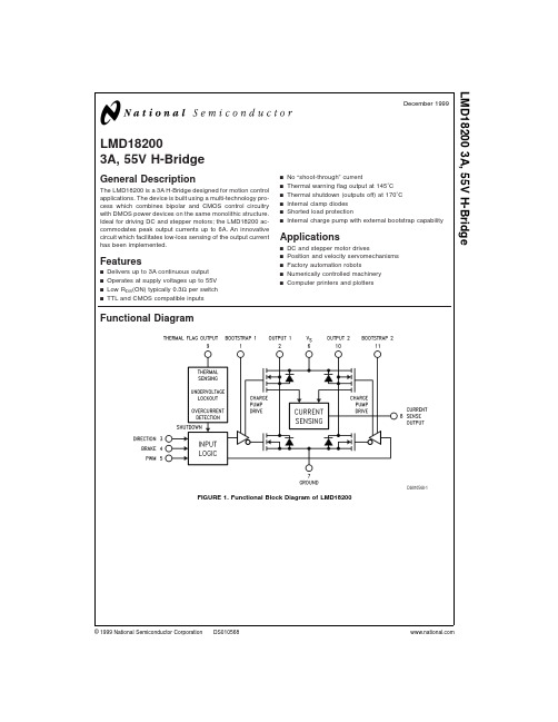
LMD182003A,55V H-BridgeGeneral DescriptionThe LMD18200is a 3A H-Bridge designed for motion control applications.The device is built using a multi-technology pro-cess which combines bipolar and CMOS control circuitry with DMOS power devices on the same monolithic structure.Ideal for driving DC and stepper motors;the LMD18200ac-commodates peak output currents up to 6A.An innovative circuit which facilitates low-loss sensing of the output current has been implemented.Featuresn Delivers up to 3A continuous output n Operates at supply voltages up to 55V n Low R DS (ON)typically 0.3Ωper switch nTTL and CMOS compatible inputsn No “shoot-through”currentn Thermal warning flag output at 145˚C n Thermal shutdown (outputs off)at 170˚C n Internal clamp diodes n Shorted load protectionnInternal charge pump with external bootstrap capabilityApplicationsn DC and stepper motor drivesn Position and velocity servomechanisms n Factory automation robotsn Numerically controlled machinery nComputer printers and plottersFunctional DiagramDS010568-1FIGURE 1.Functional Block Diagram of LMD18200December 1999LMD182003A,55V H-Bridge©1999National Semiconductor Corporation Connection Diagrams and Ordering InformationDS010568-211-Lead TO-220PackageTop ViewOrder Number LMD18200T See NS Package TA11BDS010568-2524-Lead Dual-in-Line PackageTop ViewOrder Number LMD18200-2D-QV5962-9232501VXA LMD18200-2D/8835962-9232501MXA See NS Package DA24BL M D 18200 2Absolute Maximum Ratings(Note1)If Military/Aerospace specified devices are required, please contact the National Semiconductor Sales Office/ Distributors for availability and specifications.Total Supply Voltage(V S,Pin6)60V Voltage at Pins3,4,5,8and912V Voltage at Bootstrap Pins(Pins1and11)V OUT+16V Peak Output Current(200ms)6A Continuous Output Current(Note2)3A Power Dissipation(Note3)25W Power Dissipation(T A=25˚C,Free Air)3W Junction Temperature,T J(max)150˚C ESD Susceptibility(Note4)1500V Storage Temperature,T STG−40˚C to+150˚C Lead Temperature(Soldering,10sec.)300˚COperating Ratings(Note1)Junction Temperature,T J−40˚C to+125˚C V S Supply Voltage+12V to+55VElectrical Characteristics(Note5)The following specifications apply for V S=42V,unless otherwise specified.Boldface limits apply over the entire operating temperature range,−40˚C≤T J≤+125˚C,all other limits are for T A=T J=25˚C.Symbol Parameter Conditions Typ Limit UnitsR DS(ON)Switch ON Resistance Output Current=3A(Note6)0.330.4/0.6Ω(max)R DS(ON)Switch ON Resistance Output Current=6A(Note6)0.330.4/0.6Ω(max)V CLAMP Clamp Diode Forward Drop Clamp Current=3A(Note6) 1.2 1.5V(max)V IL Logic Low Input Voltage Pins3,4,5−0.1V(min)0.8V(max)I IL Logic Low Input Current V IN=−0.1V,Pins=3,4,5−10µA(max)V IH Logic High Input Voltage Pins3,4,52V(min)12V(max)I IH Logic High Input Current V IN=12V,Pins=3,4,510µA(max)Current Sense Output I OUT=1A(Note8)377325/300µA(min)425/450µA(max) Current Sense Linearity1A≤I OUT≤3A(Note7)±6±9%Undervoltage Lockout Outputs turn OFF9V(min)11V(max)T JW Warning Flag Temperature Pin9≤0.8V,I L=2mA145˚CV F(ON)Flag Output Saturation Voltage T J=T JW,I L=2mA0.15VI F(OFF)Flag Output Leakage V F=12V0.210µA(max)T JSD Shutdown Temperature Outputs Turn OFF170˚CI S Quiescent Supply Current All Logic Inputs Low1325mA(max)t Don Output Turn-On Delay Time Sourcing Outputs,I OUT=3A300nsSinking Outputs,I OUT=3A300nst on Output Turn-On Switching Time Bootstrap Capacitor=10nFSourcing Outputs,I OUT=3A100nsSinking Outputs,I OUT=3A80nst Doff Output Turn-Off Delay Times Sourcing Outputs,I OUT=3A200nsSinking Outputs,I OUT=3A200nst off Output Turn-Off Switching Times Bootstrap Capacitor=10nFSourcing Outputs,I OUT=3A75nsSinking Outputs,I OUT=3A70nst pw Minimum Input Pulse Width Pins3,4and51µst cpr Charge Pump Rise Time No Bootstrap Capacitor20µsLMD182003Electrical Characteristics NotesNote 1:Absolute Maximum Ratings indicate limits beyond which damage to the device may occur.DC and AC electrical specifications do not apply when op-erating the device beyond its rated operating conditions.Note 2:See Application Information for details regarding current limiting.Note 3:The maximum power dissipation must be derated at elevated temperatures and is a function of T J(max),θJA ,and T A .The maximum allowable power dis-sipation at any temperature is P D(max)=(T J(max)−T A )/θJA ,or the number given in the Absolute Ratings,whichever is lower.The typical thermal resistance from junc-tion to case (θJC )is 1.0˚C/W and from junction to ambient (θJA )is 30˚C/W.For guaranteed operation T J(max)=125˚C.Note 4:Human-body model,100pF discharged through a 1.5k Ωresistor.Except Bootstrap pins (pins 1and 11)which are protected to 1000V of ESD.Note 5:All limits are 100%production tested at 25˚C.Temperature extreme limits are guaranteed via correlation using accepted SQC (Statistical Quality Control)methods.All limits are used to calculate AOQL,(Average Outgoing Quality Level).Note 6:Output currents are pulsed (t W <2ms,Duty Cycle <5%).Note 7:Regulation is calculated relative to the current sense output value with a 1A load.Note 8:Selections for tighter tolerance are available.Contact factory.Typical Performance CharacteristicsV SAT vs Flag CurrentDS010568-16R DS (ON)vs TemperatureDS010568-17R DS (ON)vs Supply VoltageDS010568-18Supply Current vs Supply VoltageDS010568-19Supply Current vs Frequency (V S =42V)DS010568-20Supply Current vsTemperature (V S =42V)DS010568-21Current Sense Output vs Load Current DS010568-22Current Sense Operating RegionDS010568-23L M D 18200 4Test CircuitSwitching Time DefinitionsPinout Description(See Connection Diagram) Pin1,BOOTSTRAP1Input:Bootstrap capacitor pin for half H-bridge number1.The recommended capacitor(10nF)is connected between pins1and2.Pin2,OUTPUT1:Half H-bridge number1output.Pin3,DIRECTION Input:See Table1.This input controls the direction of current flow between OUTPUT1and OUT-PUT2(pins2and10)and,therefore,the direction of rotation of a motor load.Pin4,BRAKE Input:See Table1.This input is used to brake a motor by effectively shorting its terminals.When braking is desired,this input is taken to a logic high level andit is also necessary to apply logic high to PWM input,pin5.The drivers that short the motor are determined by the logiclevel at the DIRECTION input(Pin3):with Pin3logic high,both current sourcing output transistors are ON;with Pin3logic low,both current sinking output transistors are ON.Alloutput transistors can be turned OFF by applying a logic highto Pin4and a logic low to PWM input Pin5;in this case onlya small bias current(approximately−1.5mA)exists at eachoutput pin.Pin5,PWM Input:See Table1.How this input(and DIREC-TION input,Pin3)is used is determined by the format of thePWM Signal.DS010568-8DS010568-9LMD182005Pinout Description(See Connection Diagram)(Continued)Pin 6,V S Power SupplyPin 7,GROUND Connection:This pin is the ground return,and is internally connected to the mounting tab.Pin 8,CURRENT SENSE Output:This pin provides the sourcing current sensing output signal,which is typically 377µA/A.Pin 9,THERMAL FLAG Output:This pin provides the ther-mal warning flag output signal.Pin 9becomes active-low at 145˚C (junction temperature).However the chip will not shut itself down until 170˚C is reached at the junction.Pin 10,OUTPUT 2:Half H-bridge number 2output.Pin 11,BOOTSTRAP 2Input:Bootstrap capacitor pin for Half H-bridge number 2.The recommended capacitor (10nF)is connected between pins 10and 11.TABLE 1.Logic Truth TablePWM Dir Brake Active Output Drivers H H L Source 1,Sink 2H L L Sink 1,Source 2L X L Source 1,Source 2H H H Source 1,Source 2H L H Sink 1,Sink 2LXHNONEApplication InformationTYPES OF PWM SIGNALSThe LMD18200readily interfaces with different forms of PWM e of the part with two of the more popular forms of PWM is described in the following paragraphs.Simple,locked anti-phase PWM consists of a single,vari-able duty-cycle signal in which is encoded both direction and amplitude information (see Figure 2).A 50%duty-cycle PWM signal represents zero drive,since the net value of voltage (integrated over one period)delivered to the load is zero.For the LMD18200,the PWM signal drives the direc-tion input (pin 3)and the PWM input (pin 5)is tied to logic high.Sign/magnitude PWM consists of separate direction (sign)and amplitude (magnitude)signals (see Figure 3).The (ab-solute)magnitude signal is duty-cycle modulated,and the absence of a pulse signal (a continuous logic low level)rep-resents zero drive.Current delivered to the load is propor-tional to pulse width.For the LMD18200,the DIRECTION in-put (pin 3)is driven by the sign signal and the PWM input (pin 5)is driven by the magnitude signal.SIGNAL TRANSITION REQUIREMENTSTo ensure proper internal logic performance,it is good prac-tice to avoid aligning the falling and rising edges of input sig-nals.A delay of at least 1µsec should be incorporated be-tween transitions of the Direction,Brake,and/or PWM input signals.A conservative approach is be sure there is at least 500ns delay between the end of the first transition and the beginning of the second transition.See Figure 4.DS010568-4FIGURE 2.Locked Anti-Phase PWM Control DS010568-5FIGURE 3.Sign/Magnitude PWM ControlL M D 18200 6Application Information(Continued)USING THE CURRENT SENSE OUTPUTThe CURRENT SENSE output(pin8)has a sensitivity of 377µA per ampere of output current.For optimal accuracy and linearity of this signal,the value of voltage generating re-sistor between pin8and ground should be chosen to limit the maximum voltage developed at pin8to5V,or less.The maximum voltage compliance is12V.It should be noted that the recirculating currents(free wheel-ing currents)are ignored by the current sense circuitry. Therefore,only the currents in the upper sourcing outputs are sensed.USING THE THERMAL WARNING FLAGThe THERMAL FLAG output(pin9)is an open collector tran-sistor.This permits a wired OR connection of thermal warn-ing flag outputs from multiple LMD18200’s,and allows the user to set the logic high level of the output signal swing to match system requirements.This output typically drives the interrupt input of a system controller.The interrupt service routine would then be designed to take appropriate steps, such as reducing load currents or initiating an orderly system shutdown.The maximum voltage compliance on the flag pin is12V.SUPPLY BYPASSINGDuring switching transitions the levels of fast current changes experienced may cause troublesome voltage tran-sients across system stray inductance.It is normally necessary to bypass the supply rail with a high quality capacitor(s)connected as close as possible to the V S Power Supply(Pin6)and GROUND(Pin7).A1µF high-frequency ceramic capacitor is recommended.Care should be taken to limit the transients on the supply pin be-low the Absolute Maximum Rating of the device.When oper-ating the chip at supply voltages above40V a voltage sup-pressor(transorb)such as P6KE62A is recommended from supply to ground.Typically the ceramic capacitor can be eliminated in the presence of the voltage suppressor.Note that when driving high load currents a greater amount of sup-ply bypass capacitance(in general at least100µF per Ampof load current)is required to absorb the recirculating cur-rents of the inductive loads.CURRENT LIMITINGCurrent limiting protection circuitry has been incorporatedinto the design of the LMD18200.With any power device it isimportant to consider the effects of the substantial surge cur-rents through the device that may occur as a result ofshorted loads.The protection circuitry monitors this increasein current(the threshold is set to approximately10Amps)and shuts off the power device as quickly as possible in theevent of an overload condition.In a typical motor driving ap-plication the most common overload faults are caused byshorted motor windings and locked rotors.Under these con-ditions the inductance of the motor(as well as any series in-ductance in the V CC supply line)serves to reduce the mag-nitude of a current surge to a safe level for the LMD18200.Once the device is shut down,the control circuitry will peri-odically try to turn the power device back on.This feature al-lows the immediate return to normal operation in the eventthat the fault condition has been removed.While the fault re-mains however,the device will cycle in and out of thermalshutdown.This can create voltage transients on the V CCsupply line and therefore proper supply bypassing tech-niques are required.The most severe condition for any power device is a direct,hard-wired(“screwdriver”)long term short from an output toground.This condition can generate a surge of currentthrough the power device on the order of15Amps and re-quire the die and package to dissipate up to500Watts ofpower for the short time required for the protection circuitryto shut off the power device.This energy can be destructive,particularly at higher operating voltages(>30V)so some precautions are in order.Proper heat sink design is essentialand it is normally necessary to heat sink the V CC supply pin(pin6)with1square inch of copper on the PCB.DS010568-24FIGURE4.Transitions in Brake,Direction,or PWM Must Be Separated By At Least1µsecLMD182007Application Information(Continued)INTERNAL CHARGE PUMP AND USE OF BOOTSTRAP CAPACITORSTo turn on the high-side (sourcing)DMOS power devices,the gate of each device must be driven approximately 8V more positive than the supply voltage.To achieve this an in-ternal charge pump is used to provide the gate drive voltage.As shown in Figure 5,an internal capacitor is alternately switched to ground and charged to about 14V,then switched to V supply thereby providing a gate drive voltage greater than V supply.This switching action is controlled by a con-tinuously running internal 300kHz oscillator.The rise time of this drive voltage is typically 20µs which is suitable for oper-ating frequencies up to 1kHz.For higher switching frequencies,the LMD18200provides for the use of external bootstrap capacitors.The bootstrap principle is in essence a second charge pump whereby a large value capacitor is used which has enough energy to quickly charge the parasitic gate input capacitance of the power device resulting in much faster rise times.The switch-ing action is accomplished by the power switches them-selves Figure 6.External 10nF capacitors,connected from the outputs to the bootstrap pins of each high-side switch provide typically less than 100ns rise times allowing switch-ing frequencies up to 500kHz.INTERNAL PROTECTION DIODESA major consideration when switching current through induc-tive loads is protection of the switching power devices from the large voltage transients that occur.Each of the four switches in the LMD18200have a built-in protection diode to clamp transient voltages exceeding the positive supply or ground to a safe diode voltage drop across the switch.The reverse recovery characteristics of these diodes,once the transient has subsided,is important.These diodes must come out of conduction quickly and the power switches must be able to conduct the additional reverse recovery current of the diodes.The reverse recovery time of the diodes protect-ing the sourcing power devices is typically only 70ns with a reverse recovery current of 1A when tested with a full 6A of forward current through the diode.For the sinking devices the recovery time is typically 100ns with 4A of reverse cur-rent under the same conditions.Typical ApplicationsFIXED OFF-TIME CONTROLThis circuit controls the current through the motor by apply-ing an average voltage equal to zero to the motor terminals for a fixed period of time,whenever the current through the motor exceeds the commanded current.This action causesthe motor current to vary slightly about an externally con-trolled average level.The duration of the Off-period is ad-justed by the resistor and capacitor combination of the LM555.In this circuit the Sign/Magnitude mode of operation is implemented (see Types of PWM Signals).DS010568-6FIGURE 5.Internal Charge Pump CircuitryDS010568-7FIGURE 6.Bootstrap CircuitryL M D 18200 8Typical Applications(Continued)TORQUE REGULATIONLocked Anti-Phase Control of a brushed DC motor.Current sense output of the LMD18200provides load sensing.The LM3525A is a general purpose PWM controller.The relationship of peak motor current to adjustment voltage is shown in Figure 10.DS010568-10FIGURE 7.Fixed Off-Time ControlDS010568-11FIGURE 8.Switching WaveformsLMD182009Typical Applications(Continued)VELOCITY REGULATIONUtilizes tachometer output from the motor to sense motor speed for a locked anti-phase control loop.The relationship of motor speed to the speed adjustment control voltage is shown in Figure 12.DS010568-12FIGURE 9.Locked Anti-Phase Control Regulates TorqueDS010568-13FIGURE 10.Peak Motor Currentvs Adjustment VoltageL M D 18200 10Typical Applications(Continued)DS010568-14FIGURE 11.Regulate Velocity with Tachometer FeedbackDS010568-15FIGURE 12.Motor Speed vsControl VoltageLMD1820011Physical Dimensionsinches (millimeters)unless otherwise noted11-Lead TO-220Power Package (T)Order Number LMD18200T NS Package Number TA11BL M D 18200 12Physical Dimensions inches(millimeters)unless otherwise noted(Continued)LIFE SUPPORT POLICYNATIONAL’S PRODUCTS ARE NOT AUTHORIZED FOR USE AS CRITICAL COMPONENTS IN LIFE SUPPORT DEVICES OR SYSTEMS WITHOUT THE EXPRESS WRITTEN APPROVAL OF THE PRESIDENT AND GENERAL COUNSEL OF NATIONAL SEMICONDUCTOR CORPORATION.As used herein:1.Life support devices or systems are devices orsystems which,(a)are intended for surgical implantinto the body,or(b)support or sustain life,andwhose failure to perform when properly used inaccordance with instructions for use provided in thelabeling,can be reasonably expected to result in asignificant injury to the user.2.A critical component is any component of a lifesupport device or system whose failure to performcan be reasonably expected to cause the failure ofthe life support device or system,or to affect itssafety or effectiveness.National SemiconductorCorporationAmericasTel:1-800-272-9959Fax:1-800-737-7018Email:support@National SemiconductorEuropeFax:+49(0)180-5308586Email:europe.support@Deutsch Tel:+49(0)180-5308585English Tel:+49(0)180-5327832Français Tel:+49(0)180-5329358Italiano Tel:+49(0)180-5341680National SemiconductorAsia Pacific CustomerResponse GroupTel:65-2544466Fax:65-2504466Email:sea.support@National SemiconductorJapan Ltd.Tel:81-3-5639-7560Fax:81-3-5639-7507 24-Lead Dual-in-Line PackageOrder Number LMD18200-2D-QV5962-9232501VXALMD18200-2D/8835962-9232501MXANS Package Number DA24BLMD182003A,55VH-Bridge National does not assume any responsibility for use of any circuitry described,no circuit patent licenses are implied and National reserves the right at any time without notice to change said circuitry and specifications.。
5962-8405601VDA中文资料

PACKAGING INFORMATIONOrderable Device Status(1)PackageType PackageDrawingPins PackageQtyEco Plan(2)Lead/Ball Finish MSL Peak Temp(3)5962-8405601VCA ACTIVE CDIP J141None Call TI Level-NC-NC-NC 5962-8405601VDA ACTIVE CFP W141None Call TI Level-NC-NC-NC 84056012A ACTIVE LCCC FK201None Call TI Level-NC-NC-NC 8405601CA ACTIVE CDIP J141None Call TI Level-NC-NC-NC 8405601DA ACTIVE CFP W141None Call TI Level-NC-NC-NC JM38510/65302B2A ACTIVE LCCC FK201None Call TI Level-NC-NC-NC JM38510/65302BCA ACTIVE CDIP J141None Call TI Level-NC-NC-NC JM38510/65302BDA ACTIVE CFP W141None Call TI Level-NC-NC-NC SN54HC74J ACTIVE CDIP J141None Call TI Level-NC-NC-NC SN74HC74ADBLE OBSOLETE SSOP DB14None Call TI Call TISN74HC74D ACTIVE SOIC D1450Pb-Free(RoHS)CU NIPDAU Level-2-260C-1YEAR/Level-1-235C-UNLIMSN74HC74DBLE OBSOLETE SSOP DB14None Call TI Call TISN74HC74DBR ACTIVE SSOP DB142000Pb-Free(RoHS)CU NIPDAU Level-2-260C-1YEAR/Level-1-235C-UNLIMSN74HC74DR ACTIVE SOIC D142500Green(RoHS&no Sb/Br)CU NIPDAU Level-1-260C-UNLIMSN74HC74DT ACTIVE SOIC D14250Pb-Free(RoHS)CU NIPDAU Level-2-260C-1YEAR/Level-1-235C-UNLIMSN74HC74N ACTIVE PDIP N1425Pb-Free(RoHS)CU NIPDAU Level-NC-NC-NC SN74HC74N3OBSOLETE PDIP N14None Call TI Call TISN74HC74NSR ACTIVE SO NS142000Pb-Free(RoHS)CU NIPDAU Level-2-260C-1YEAR/Level-1-235C-UNLIMSN74HC74PW ACTIVE TSSOP PW1490Pb-Free(RoHS)CU NIPDAU Level-1-250C-UNLIMSN74HC74PWLE OBSOLETE TSSOP PW14None Call TI Call TISN74HC74PWR ACTIVE TSSOP PW142000Pb-Free(RoHS)CU NIPDAU Level-1-250C-UNLIMSN74HC74PWT ACTIVE TSSOP PW14250Pb-Free(RoHS)CU NIPDAU Level-1-250C-UNLIM SNJ54HC74FK ACTIVE LCCC FK201None Call TI Level-NC-NC-NC SNJ54HC74J ACTIVE CDIP J141None Call TI Level-NC-NC-NC SNJ54HC74W ACTIVE CFP W141None Call TI Level-NC-NC-NC (1)The marketing status values are defined as follows:ACTIVE:Product device recommended for new designs.LIFEBUY:TI has announced that the device will be discontinued,and a lifetime-buy period is in effect.NRND:Not recommended for new designs.Device is in production to support existing customers,but TI does not recommend using this part in a new design.PREVIEW:Device has been announced but is not in production.Samples may or may not be available.OBSOLETE:TI has discontinued the production of the device.(2)Eco Plan-May not be currently available-please check /productcontent for the latest availability information and additional product content details.None:Not yet available Lead(Pb-Free).Pb-Free(RoHS):TI's terms"Lead-Free"or"Pb-Free"mean semiconductor products that are compatible with the current RoHS requirements for all6substances,including the requirement that lead not exceed0.1%by weight in homogeneous materials.Where designed to be soldered at high temperatures,TI Pb-Free products are suitable for use in specified lead-free processes.Green(RoHS&no Sb/Br):TI defines"Green"to mean"Pb-Free"and in addition,uses package materials that do not contain halogens, including bromine(Br)or antimony(Sb)above0.1%of total product weight.(3)MSL,Peak Temp.--The Moisture Sensitivity Level rating according to the JEDECindustry standard classifications,and peak solder temperature.Important Information and Disclaimer:The information provided on this page represents TI's knowledge and belief as of the date that it is provided.TI bases its knowledge and belief on information provided by third parties,and makes no representation or warranty as to the accuracy of such information.Efforts are underway to better integrate information from third parties.TI has taken and continues to take reasonable steps to provide representative and accurate information but may not have conducted destructive testing or chemical analysis on incoming materials and chemicals.TI and TI suppliers consider certain information to be proprietary,and thus CAS numbers and other limited information may not be available for release.In no event shall TI's liability arising out of such information exceed the total purchase price of the TI part(s)at issue in this document sold by TI to Customer on an annual basis.元器件交易网IMPORTANT NOTICETexas Instruments Incorporated and its subsidiaries (TI) reserve the right to make corrections, modifications,enhancements, improvements, and other changes to its products and services at any time and to discontinueany product or service without notice. Customers should obtain the latest relevant information before placingorders and should verify that such information is current and complete. All products are sold subject to TI’s termsand conditions of sale supplied at the time of order acknowledgment.TI warrants performance of its hardware products to the specifications applicable at the time of sale inaccordance with TI’s standard warranty. T esting and other quality control techniques are used to the extent TIdeems necessary to support this warranty. Except where mandated by government requirements, testing of allparameters of each product is not necessarily performed.TI assumes no liability for applications assistance or customer product design. Customers are responsible fortheir products and applications using TI components. T o minimize the risks associated with customer productsand applications, customers should provide adequate design and operating safeguards.TI does not warrant or represent that any license, either express or implied, is granted under any TI patent right,copyright, mask work right, or other TI intellectual property right relating to any combination, machine, or processin which TI products or services are used. Information published by TI regarding third-party products or servicesdoes not constitute a license from TI to use such products or services or a warranty or endorsement thereof.Use of such information may require a license from a third party under the patents or other intellectual propertyof the third party, or a license from TI under the patents or other intellectual property of TI.Reproduction of information in TI data books or data sheets is permissible only if reproduction is withoutalteration and is accompanied by all associated warranties, conditions, limitations, and notices. Reproductionof this information with alteration is an unfair and deceptive business practice. TI is not responsible or liable forsuch altered documentation.Resale of TI products or services with statements different from or beyond the parameters stated by TI for thatproduct or service voids all express and any implied warranties for the associated TI product or service andis an unfair and deceptive business practice. TI is not responsible or liable for any such statements.Following are URLs where you can obtain information on other Texas Instruments products and applicationsolutions:Products ApplicationsAmplifiers Audio /audioData Converters Automotive /automotiveDSP Broadband /broadbandInterface Digital Control /digitalcontrolLogic Military /militaryPower Mgmt Optical Networking /opticalnetworkMicrocontrollers Security /securityTelephony /telephonyVideo & Imaging /videoWireless /wirelessMailing Address:Texas InstrumentsPost Office Box 655303 Dallas, Texas 75265Copyright 2005, Texas Instruments Incorporated。
5962-0053901QYA中文资料

Copyright 2002, Texas Instruments Incorporated
On products compliant to MIL−PRF−38535, all parameters are tested unless otherwise noted. On all other products, production processing does not necessarily include testing of all parameters.
元器件交易网
SM320VC33, SMJ320VC33 DIGITAL SIGNAL PROCESSOR
SGUS034E - FEBRUARY 2001 - REVISED OCTOBER 2002
D High-Performance Floating-Point Digital
Signal Processor (DSP): - SM/SMJ320VC33-150 - 13-ns Instruction Cycle Time - 150 Million Floating-Point Operations Per Second (MFLOPS) - 75 Million Instructions Per Second (MIPS) 34K × 32-Bit (1.1-Mbit) On-Chip Words of Dual-Access Static Random-Access Memory (SRAM) Configured in 2 × 16K plus 2 × 1K Blocks to improve Internal Performance Generator Very Low Power: < 200 mW @ 150 MFLOPS 32-Bit High-Performance CPU 16-/32-Bit Integer and 32-/40-Bit Floating-Point Operations Four Internally Decoded Page Strobes to Simplify Interface to I/O and Memory Devices Boot-Program Loader EDGEMODE Selectable External Interrupts 32-Bit Instruction Word, 24-Bit Addresses Eight Extended-Precision Registers Fabricated Using the 0.18-µm (leff-Effective Gate Length) TImeline Technology by Texas Instruments (TI)
5962-89957012A中文资料

The UC1637 is a pulse width modulator circuit intended to be used for a variety of PWM motor drive and amplifier applications requiring either uni-directional or bi-directional drive circuits. When used to replace conventional drivers, this circuit can increase efficiency and reduce component costs for many applications. All necessary circuitry is included to generate an analog error signal and modulate two bi-directional pulse train outputs in proportion to the error signal magnitude and polarity.This monolithic device contains a sawtooth oscillator, error amplifier, and two PWM comparators with ±100mA output stages as standard features. Protection circuitry includes under-voltage lockout, pulse-by-pulse current limiting, and a shutdown port with a 2.5V temperature compensated threshold.The UC1637 is characterized for operation over the full military temperature range of -55°C to +125°C, while the UC2637 and UC3637 are characterized for -25°C to +85°C and 0°C to +70°C, respectively.Switched Mode Controller for DC Motor DriveUC2637UC3637BLOCK DIAGRAM•Single or Dual Supply Operation•±2.5V to ±20V Input Supply Range•±5% Initial Oscillator Accuracy; ± 10% Over Temperature•Pulse-by-Pulse Current Limiting•Under-Voltage Lockout •Shutdown Input withTemperature Compensated 2.5V Threshold •Uncommitted PWM Comparators for Design Flexibility•Dual 100mA, Source/Sink Output DriversSupply Voltage (±Vs). . . . . . . . . . . . . . . . . . . . . . . . . . . . . . . . . . . . . . . . . . . . . . . . . . . ±20V Output Current, Source/Sink (Pins 4, 7). . . . . . . . . . . . . . . . . . . . . . . . . . . . . . . . . . . 500mA Analog Inputs (Pins 1, 2, 3, 8, 9, 10, 11 12, 13, 14, 15, 16). . . . . . . . . . . . . . . . . . . . . . . ±Vs Error Amplifier Output Current (Pin 17). . . . . . . . . . . . . . . . . . . . . . . . . . . . . . . . . . . ±20mA Oscillator Charging Current (Pin 18). . . . . . . . . . . . . . . . . . . . . . . . . . . . . . . . . . . . . . . -2mA Power Dissipation at T A = 25°C (Note 2). . . . . . . . . . . . . . . . . . . . . . . . . . . . . . . . 1000mW Power Dissipation at T C = 25°C (Note 2). . . . . . . . . . . . . . . . . . . . . . . . . . . . . . . . 2000mW Storage Temperature Range . . . . . . . . . . . . . . . . . . . . . . . . . . . . . . . . . . . -65°C to +150°C Lead Temperature (Soldering, 10 Seconds). . . . . . . . . . . . . . . . . . . . . . . . . . . . . . . . +300°C Note 1:Currents are positive into, negative out of the specified terminal.Note 2: Consult Packaging Section of Databook for thermal limitations and considerationsof package.FEATURESABSOLUTE MAXIMUM RATINGS (Note 1)DESCRIPTIONUC3637PACKAGE PIN FUNCTION FUNCTION PIN+V TH 1C T 2-V TH 3A OUT 4-V S 5N/C 6+V S 7B OUT 8+B IN 9-B IN 10-A IN 11+A IN 12+C/L 13-C/L14SHUTDOWN 15N/C 16+E/A 17-E/A18E/A OUTPUT 19I SET 20PLCC-20, LCC-20(TOP VIEW) Q, L PackagesELECTRICAL CHARACTERISTICS:PARAMETERTEST CONDITIONSUC1637/UC2637UC3637UNITSMINTYPMAXMINTYPMAXOscillator Initial Accuracy T J = 25°C (Note 6)9.41010.691011kHz Voltage Stability V S = ±5V to ±20V, V PIN 1 = 3V, V PIN 3 = -3V5757%Temperature Stability Over Operating Range (Note 3)0.520.52%+V TH Input Bias Current V PIN 2 = 6V -100.110-100.110µA -V TH Input Bias Current V PIN 2 = 0V-10-0.5-10-0.5µA +V TH, -V TH Input Range +V S -2-V S +2+V S -2-V S +2VError Amplifier Input Offset Voltage V CM = 0V 1.55 1.510mV Input Bias Current V CM = 0V 0.550.55µA Input Offset Current V CM = 0V0.110.11µA Common Mode Range V S = ±2.5 to 20V -V S +2+V S-V S +2+V SV Open Loop Voltage Gain R L = 10k7510080100dB Slew Rate1515V/µS Unity Gain Bandwidth 22MHz CONNECTION DIAGRAMUnless otherwise stated, these specifications apply for T A = -55°C to +125°C for theUC1637; -25°C to +85°C for the UC2637; and 0°C to +70°C for the UC3637; +V S =+15V, -V S = - 15V, +V TH = 5V, -V TH = -5V, R T = 16.7k Ω, C T = 1500pF, T A =T J.DIL-18 (TOP VIEW)J or N PackageSOIC-20 (TOP VIEW) DW PackageELECTRICAL CHARACTERISTICS:PARAMETERS TEST CONDITIONS UC1637/UC2637UC3637UNITSMIN TYP MAX MIN TYP MAXError Amplifier (Continued)Output Sink Current V PIN 17 = 0V-50-20-50-20mA Output Source Current V PIN 17 = 0V511511mA High Level Output Voltage1313.61313.6V Low Level Output Voltage-14.8-13-14.8-13V PWM ComparatorsInput Offset Voltage V CM = 0V2020mV Input Bias Current V CM = 0V210210µA Input Hysteresis V CM = 0V1010mV Common Mode range V S = ±5V to ±20V-V S+1+V S-2-V S+1+V S-2V Current LimitInput Offset Voltage V CM = 0V, T J = 25°C190200210180200220mV Input Offset Voltage T.C.-0.2-0.2mV/°C Input Bias Current-10-1.5-10-1.5µA Common Mode Range V S = ±2.5V to ±20V-V S+V S-3-V S+V S-3V ShutdownShutdown Threshold(Note 4)-2.3-2.5-2.7-2.3-2.5-2.7V Hysteresis4040mV Input Bias Current V PIN 14 = +V S to -V S-10-0.5-10-0.5µA Under-Voltage LockoutStart Threshold(Note 5) 4.15 5.0 4.15 5.0V Hysteresis0.250.25mV Total Standby CurrentSupply Current8.5158.515mA Output SectionOutput Low Level I SINK = 20mA-14.9-13-14.9-13VI SINK = 100mA-14.5-13-14.5-13Output High Level I SOURCE = 20mA1313.51313.5VI SOURCE = 100mA1213.51213.5Rise Time(Note 3) C L = Inf, T J = 25°C100600100600ns Fall Time(Note 3) C L = Inf, T J = 25°C100300100300ns Note 3:These parameters, although guaranteed over the recommended operating conditions, are not 100% tested in production. Note 4:Parameter measured with respect to +V S (Pin 6).Note 5:Parameter measured at +V S (Pin 6) with respect to -V S (Pin 5).Note 6:R T and C T referenced to Ground.FUNCTIONAL DESCRIPTIONFollowing is a description of each of the functional blocks shown in the Block Diagram.OscillatorThe oscillator consists of two comparators, a charging and discharging current source, a current source set ter-minal, l SET and a flip-flop. The upper and lower threshold minal voltage is buffered internally and also applied to the l SET terminal to develop the capacitor charging current through R T. If R T is referenced to -V S as shown in Figure 1, both the threshold voltage and charging current will vary proportionally to the supply differential, and the oscil-lator frequency will remain constant. The triangle wave-Unless otherwise stated, these specifications apply for T A = -55°C to +125°C for the UC1637; -25°C to +85°C for the UC2637; and 0°C to +70°C for the UC3637: V S = +15V, -V S = - 15V, +V TH = 5V, -V TH = -5V, R T = 16.7kΩ, C T = 1500pF, T A=T J.MODULATION SCHEMESCase A Zero Deadtime (Equal voltage on Pin 9 and Pin 11)In this configuration, maximum holding torque or stiffness and position accuracy is achieved. However, the power in-put into the motor is increased. Figure 3A shows this con-figuration.Case B Small Deadtime (Voltage on Pin 9 > Pin 11)A small differential voltage between Pin 9 and 11 provides the necessary time delay to reduce the chances of mo-mentary short circuit in the output stage during transi-tions, especially where power-amplifiers are used. Refer to Figure 3B.Case C Increased Deadtime and Deadband Mode (Voltage on Pin 9 > Pin 11)With the reduction of stiffness and position accuracy, the power input into the motor around the null point of the servo loop can be reduced or eliminated by widening the window of the comparator circuit to a degree of accep-tance. Where position accuracy and mechanical stiffness is unimportant, deadband operation can be used. This is PWM ComparatorsT wo comparators are provided to perform pulse width modulation for each of the output drivers. Inputs are un-committed to allow maximum flexibility. The pulse width of the outputs A and B is a function of the sign and ampli-tude of the error signal. A negative signal at Pin 10 and 8will lengthen the high state of output A and shorten the high state of output B. Likewise, a positive error signal re-verses the procedure. T ypically, the oscillator waveform is compared against the summation of the error signal andthe level set on Pin 9 and 11.Figure 1.Oscillator SetupFigure 2. Comparator BiasingOutput DriversEach output driver is capable of both sourcing and sinking 100mA steady state and up to 500mA on a pulsed basis for rapid switching of either POWERFET or bipolar tran-sistors. Output levels are typically -V S + 0.2V @50mA low level and +V S - 2.0V @50mA high level.Error AmplifierThe error amplifier consists of a high slew rate (15V/µs)op-amp with a typical 1MHz bandwidth and low output im-pedance. Depending on the ±V S supply voltage, the com-mon mode input range and the voltage output swing is within 2V of the V S supply.Under-Voltage LockoutAn under-voltage lockout circuit holds the outputs in the low state until a minimum of 4V is reached. At this point,all internal circuitry is functional and the output drivers are enabled. If external circuitry requires a higher starting volt-age, an over-riding voltage can be programmed through the shutdown terminal as shown in Figure 4.Figure 3.Modulation Schemes Showing (A) Zero Deadtime (B) Deadtime and (C) Deadband ConfigurationsShutdown ComparatorThe shutdown terminal may be used for implementingvarious shutdown and protection schemes. By pulling theterminal more than 2.5V below V IN, the output drivers willbe enabled. This can be realized using an open collectorgate or NPN transistor biased to either ground or thenegative supply. Since the threshold is temperature stabi-lized, the comparator can be used as an accurate lowvoltage lockout (Figure 4) and/or delayed start as in Fig-ure 5. In the shutdown mode the outputs are held in thelow state.Current LimitA latched current limit amplifier with an internal 200mV-V S to within 3V of the +V S supply while providing excel-lent noise rejection. Figure 6 shows a typical currentsense circuit.Figure 4.External Under-Voltage LockoutFigure 5.Delayed Start-UpFigure 7. Bi-Directional Motor Drive with Speed Control Power-AmplifierFigure 8.Single Supply Position Servo Motor DrivePACKAGING INFORMATIONOrderable Device Status(1)PackageType PackageDrawingPins PackageQtyEco Plan(2)Lead/Ball Finish MSL Peak Temp(3)5962-89957012A ACTIVE LCCC FK201TBD POST-PLATE Level-NC-NC-NC 5962-8995701VA ACTIVE CDIP J181TBD A42SNPB Level-NC-NC-NC UC1637J ACTIVE CDIP J181TBD A42SNPB Level-NC-NC-NC UC1637J883B ACTIVE CDIP J181TBD A42SNPB Level-NC-NC-NC UC1637L ACTIVE LCCC FK201TBD POST-PLATE Level-NC-NC-NC UC1637L883B ACTIVE LCCC FK201TBD POST-PLATE Level-NC-NC-NCUC2637DW ACTIVE SOIC DW2025Green(RoHS&no Sb/Br)CU NIPDAU Level-2-260C-1YEARUC2637DWG4ACTIVE SOIC DW2025Green(RoHS&no Sb/Br)CU NIPDAU Level-2-260C-1YEARUC2637DWTR ACTIVE SOIC DW202000Green(RoHS&no Sb/Br)CU NIPDAU Level-2-260C-1YEAR UC2637J ACTIVE CDIP J181TBD A42SNPB Level-NC-NC-NCUC2637N ACTIVE PDIP N1820Green(RoHS&no Sb/Br)CU NIPDAU Level-NC-NC-NCUC2637NG4ACTIVE PDIP N1820Green(RoHS&no Sb/Br)CU NIPDAU Level-NC-NC-NCUC2637Q ACTIVE PLCC FN2046Green(RoHS&no Sb/Br)CU SN Level-2-260C-1YEARUC2637QTR ACTIVE PLCC FN201000Green(RoHS&no Sb/Br)CU SN Level-2-260C-1YEARUC3637DW ACTIVE SOIC DW2025Green(RoHS&no Sb/Br)CU NIPDAU Level-2-260C-1YEARUC3637DWTR ACTIVE SOIC DW202000Green(RoHS&no Sb/Br)CU NIPDAU Level-2-260C-1YEARUC3637DWTRG4ACTIVE SOIC DW202000Green(RoHS&no Sb/Br)CU NIPDAU Level-2-260C-1YEAR UC3637J ACTIVE CDIP J181TBD A42SNPB Level-NC-NC-NCUC3637N ACTIVE PDIP N1820Green(RoHS&no Sb/Br)CU NIPDAU Level-NC-NC-NCUC3637NG4ACTIVE PDIP N1820Green(RoHS&no Sb/Br)CU NIPDAU Level-NC-NC-NCUC3637Q ACTIVE PLCC FN2046Green(RoHS&no Sb/Br)CU SN Level-2-260C-1YEAR(1)The marketing status values are defined as follows:ACTIVE:Product device recommended for new designs.LIFEBUY:TI has announced that the device will be discontinued,and a lifetime-buy period is in effect.NRND:Not recommended for new designs.Device is in production to support existing customers,but TI does not recommend using this part in a new design.PREVIEW:Device has been announced but is not in production.Samples may or may not be available.OBSOLETE:TI has discontinued the production of the device.(2)Eco Plan-The planned eco-friendly classification:Pb-Free(RoHS)or Green(RoHS&no Sb/Br)-please check /productcontent for the latest availability information and additional product content details.TBD:The Pb-Free/Green conversion plan has not been defined.Pb-Free(RoHS):TI's terms"Lead-Free"or"Pb-Free"mean semiconductor products that are compatible with the current RoHS requirements for all6substances,including the requirement that lead not exceed0.1%by weight in homogeneous materials.Where designed to be soldered at high temperatures,TI Pb-Free products are suitable for use in specified lead-free processes.Green(RoHS&no Sb/Br):TI defines"Green"to mean Pb-Free(RoHS compatible),and free of Bromine(Br)and Antimony(Sb)based flame retardants(Br or Sb do not exceed0.1%by weight in homogeneous material)(3)MSL,Peak Temp.--The Moisture Sensitivity Level rating according to the JEDEC industry standard classifications,and peak solder temperature.Important Information and Disclaimer:The information provided on this page represents TI's knowledge and belief as of the date that it is provided.TI bases its knowledge and belief on information provided by third parties,and makes no representation or warranty as to the accuracy of such information.Efforts are underway to better integrate information from third parties.TI has taken and continues to take reasonable steps to provide representative and accurate information but may not have conducted destructive testing or chemical analysis on incoming materials and chemicals.TI and TI suppliers consider certain information to be proprietary,and thus CAS numbers and other limited information may not be available for release.In no event shall TI's liability arising out of such information exceed the total purchase price of the TI part(s)at issue in this document sold by TI to Customer on an annual basis.IMPORTANT NOTICETexas Instruments Incorporated and its subsidiaries (TI) reserve the right to make corrections, modifications, enhancements, improvements, and other changes to its products and services at any time and to discontinue any product or service without notice. Customers should obtain the latest relevant information before placing orders and should verify that such information is current and complete. All products are sold subject to TI’s terms and conditions of sale supplied at the time of order acknowledgment.TI warrants performance of its hardware products to the specifications applicable at the time of sale in accordance with TI’s standard warranty. T esting and other quality control techniques are used to the extent TI deems necessary to support this warranty. Except where mandated by government requirements, testing of all parameters of each product is not necessarily performed.TI assumes no liability for applications assistance or customer product design. Customers are responsible for their products and applications using TI components. T o minimize the risks associated with customer products and applications, customers should provide adequate design and operating safeguards.TI does not warrant or represent that any license, either express or implied, is granted under any TI patent right, copyright, mask work right, or other TI intellectual property right relating to any combination, machine, or process in which TI products or services are used. Information published by TI regarding third-party products or services does not constitute a license from TI to use such products or services or a warranty or endorsement thereof. Use of such information may require a license from a third party under the patents or other intellectual property of the third party, or a license from TI under the patents or other intellectual property of TI.Reproduction of information in TI data books or data sheets is permissible only if reproduction is without alteration and is accompanied by all associated warranties, conditions, limitations, and notices. Reproduction of this information with alteration is an unfair and deceptive business practice. TI is not responsible or liable for such altered documentation.Resale of TI products or services with statements different from or beyond the parameters stated by TI for that product or service voids all express and any implied warranties for the associated TI product or service and is an unfair and deceptive business practice. TI is not responsible or liable for any such statements. Following are URLs where you can obtain information on other Texas Instruments products and application solutions:Products ApplicationsAmplifiers Audio /audioData Converters Automotive /automotiveDSP Broadband /broadbandInterface Digital Control /digitalcontrolLogic Military /militaryPower Mgmt Optical Networking /opticalnetwork Microcontrollers Security /securityTelephony /telephonyVideo & Imaging /videoWireless /wirelessMailing Address:Texas InstrumentsPost Office Box 655303 Dallas, Texas 75265Copyright 2005, Texas Instruments Incorporated。
lm596中文资料

LM2596开关电压调节器LM2596开关电压调节器是降压型电源管理单片集成电路,能够输出3A的驱动电流,同时具有很好的线性和负载调节特性。
固定输出版本有3.3V、5V、12V,可调版本可以输出小于37V的各种电压。
该器件内部集成频率补偿和固定频率发生器,开关频率为150KHz,与低频开关调节器相比较,可以使用更小规格的滤波元件。
由于该器件只需4个外接元件,可以使用通用的标准电感,这更优化了LM2596的使用,极大地简化了开关电源电路的设计。
其封装形式包括标准的5脚TO-220封装(DIP)和5脚TO-263表贴封装(SMD)。
该器件还有其他一些特点:在特定的输入电压和输出负载的条件下,输出电压的误差可以保证在±4%的范围内,振荡频率误差在±15%的范围内;可以用仅80μA的待机电流,实现外部断电;具有自我保护电路(一个两级降频限流保护和一个在异常情况下断电的过温完全保护电路)特点Ć 3.3V、5V、12V的固定电压输出和可调电压输出Ć可调输出电压范围1.2V~37V±4%Ć输出线性好且负载可调节Ć输出电流可高达3AĆ输入电压可高达40VĆ采用150KHz的内部振荡频率,属于第二代开关电压调节器,功耗小、效率高Ć低功耗待机模式,I Q的典型值为80μAĆTTL断电能力Ć具有过热保护和限流保护功能Ć封装形式:TO-220(T)和TO-263(S)Ć外围电路简单,仅需4个外接元件,且使用容易购买的标准电感应用领域Ć高效率降压调节器Ć单片开关电压调节器Ć正、负电压转换器典型应用(固定输出)LM2596□-5.0管脚图极限参数名称范围单位最大电源电压45V 脚输入电压-0.3~25V “反馈”脚电压-0.3~25V 到地的输出电压(静态)-1V 功耗由内部限定--储存温度-65~150℃静电释放(人体放电1)2000V 气流焊(60秒)215℃TO-263红外线焊接(10秒)245℃焊接时的管脚温度TO-220波峰焊/电烙铁焊接(10秒)260℃最高结温150℃温度范围-40~125℃工作条件电源电压4.5~40V注1:人体放电模式相当于一个100PF 的电容通过一个1.5K 的电阻向每个管脚放电。
5962-0052201HXC中文资料

1Size (max.): 1.075 x 1.075 x 0.270 inches (27.31 x 27.31 x 6.86 mm)Weight:15 grams maximum.Screening: Standard, ES, or 883 (Class H).DESCRIPTIONThe MSA Series™of high frequency DC/DC converters offers a new standard of performance for low power, military/aerospace grade DC/DC converters. MSA parts provide up to 5 watts output power over the full military temperature range with up to 76% efficiency.Thick-film hybrid techniques provide military/aerospace reliability levels and optimum miniaturization. The hermetically sealed case is only 1.075 by 1.075 inches — with a height of only 0.270 inches.Power density for the MSA Series parts is 16 watts per cubic inch.The MSA Series’small size, low height, and hermetically sealed metal enclosures make them ideal for use in military, aerospace and other high reliability applications. Units are available with standard,screening, “ES”, and fully compliant SMD “883” screening. See page 8 for screening options and descriptions.C ONVERTERD ESIGNThe MSA converters are switching regulators that use a flyback converter design with a constant switching frequency of 550 kHz.They are regulated, isolated units using a pulse width modulated topology and built as high reliability thick-film hybrids. Isolation between input and output circuits is provided with a transformer in the forward power path and an optical link in the feedback control loop. Excellent input line transient response and audio rejection is achieved by an advanced feed-forward compensation technique.Negative output regulation is maintained by tightly coupled magnetics. Up to 4 watts, 80% of the total output power, is available from either output, provided that the opposite output is simultane-ously carrying 20% of the total power. Each output must carry a minimum of 20% of the total output power in order to maintain spec-ified regulation on the negative output. Predictable current limit is accomplished by direct monitoring of the output load current, which results in a constant current output above the overload point.Internal input and output filters eliminate the need for external capacitors.W IDE V OLTAGE R ANGEThe MSA converters are designed to provide full power operation over a full 16 to 40 VDC voltage range. Operation below 16 volts,including MIL-STD-704E emergency power conditions is possible with derated power. Please refer to the low line dropout graphs (Figures 17 and 18) for details. A low voltage lockout feature keeps the converter shutdown below approximately 13 VDC to ensure smooth initialization.I MPROVED D YNAMIC R ESPONSEThe MSA feed-forward compensation system provides excellent dynamic response and noise rejection. Audio rejection is typically 50dB. The minimum to maximum step line transient response is typi-cally less than 1%.I NHIBIT F UNCTIONMSA converters provide a TTL open collector-compatible inhibit feature that can be used to disable internal switching and inhibit the unit’s output. Inhibiting in this manner results in low standby current,and no generation of switching noise.The converter is inhibited when the TTL compatible low (≤0.8 V) is applied to the inhibit pin. The unit is enabled when the pin, which is internally connected to a pull-up resistor, is left unconnected or is connected to an open collector gate. The open circuit output voltage associated with the inhibit pin is 9 to 11 V. In the inhibit mode, a maximum of 4 mA must be sunk from the inhibit pin.U NDERVOLTAGE L OCKOUT AND T RANSIENT P ROTECTIONUndervoltage lockout helps keep system current levels low during initialization or re-start operations. They can withstand short term transients of up to 50 volts without damage.MSA SERIES5 WATTF EATURES•–55°to +125°C operation •16 to 40 VDC input •Fully isolated•Optocoupler feedback•Fixed frequency, 550 kHz typical (400 kHz typ. 60 V output model)•Topology – Flyback••Inhibit function•Indefinite short circuit protection •Up to 76% efficiency, 16 W/in 3RECOMMENDED OPERATING CONDITIONSTYPICAL CHARACTERISTICSINHIBITABSOLUTE MAXIMUM RATINGSInput Voltage •16 to 40 V Output Power •5 wattsLead Soldering Temperature (10 sec per lead)•300°CStorage Temperature Range (Case)•–65°C to +135°C2MSA SERIES 5 WATTDC/DC C ONVERTERSOutput Voltage Temperature Coefficient •100 ppm/°C typicalInput to Output Capacitance •50 pF typical Isolation•100 megohm minimum at 500 V Audio Rejection •50 dB typicalConversion Frequency•550 kHz typical (400 kHz 60 V model)450 kHz min, 600 kHz max350 kHz min, 450 kHz max 60 V model Inhibit Pin Voltage (unit enabled)•9to 11 VInput Voltage Range•16 to 40 VDC continuous•50 V for up to 50 msec transient Case Operating Temperature (Tc)•–55°C to +125°C full power •–55°C to +135°C absoluteDerating Output Power/Current (Tc)•Linearly from 100% at 125°C to 0% at 135°CElectrical Characteristics:25°C Tc,28 VDC Vin,100% load,unless otherwise specified.Inhibit TTL Open Collector •Logic low (output disabled)Logic low voltage ≤0.8 V max Inhibit pin current 4 mA max •Referenced to input common •Logic high (output enabled)Open collectorNotes1.M SA2860S specifications are at 25°Tc only,contact your Interpoint representative for more information on over temperature specs.2.Line regulation for /ES and non /ES 2805S models at 16 to 17 V IN and 110°C to 125°C (case) is 5% (max).3.Indefinite short circuit protection not guaranteed above 125°C (case).4.Recovery time is measured from application of the transient to point at which V OUT is within 1% of V OUT at final value.5.Transition time >10µs.SINGLE OUTPUT MODELS MSA2805S MSA285R2S MSA2812S MSA2815S MSA2860S 1PARAM ETER CONDITIONS M IN TYP M AX M IN TYP M AX M IN TYP M AX M IN TYP M AX M IN TYP M AX UNITS OUTPUT VOLTAGE Tc = –55°C TO +125°C 4.95 5.00 5.05 5.15 5.20 5.2511.8812.0012.1214.8515.0015.1559.160.0060.9VDC OUTPUT CURRENTTc = –55°C TO +125°C V IN = 16 TO 40 VDC 0—1000—962—417—333—20mAOUTPUT POWER V IN = 16 TO 40 VDC Tc = –55°C TO +125°C ——5——5——5——5—— 1.2W OUTPUT RIPPLE VOLTAGE10 kHz - 2 MHz —125350—110335—50200—50170——300mV p-p LINE REGULATION V IN = 16 TO 40 VDC Tc = –55°C TO +125°C —10502—1050—1050—1050——300mV LOAD REGULATION NO LOAD TO FULL Tc = –55°C TO +125°C —1050—1050—1050—1050——300mV INPUT VOLTAGE Tc = –55°C TO +125°CNO LOAD TO FULL CONTINUOUS 162840162840162840162840162840VDC TRANSIENT 50 ms0—500—500—500—500—50V INPUT CURRENT NO LOAD —2740—2840—2942—3144——30T c = –55°C TO +125°C FULL LOAD —250——250——235——235——72—mA INHIBITED —35—35—35—35—35INPUT RIPPLE 10 kHz - 10 MHz —25100—25100—25100—25100——90mA p-p CURRENT Tc = –55°C TO +125°C—30150—30150—30150—30150———EFFICIENCY 6671—6671—7076—7176—7075—%LOAD FAULT 3, 4POWER DISSIPATION— 1.5 2.0— 1.5 2.0— 1.2 1.9— 1.2 1.8———W SHORT CIRCUIT RECOVERY —12.525— 1.525—110—110———ms STEP LOAD 50% - 100% - 50%RESPONSE 4, 5TRANSIENT —100250—100250—150375—200500———mV pk RECOVERY—100250—100250—200500—200500———µs STEP LINE TRANSIENT RESPONSE 4, 516 TO 40 V IN—50150—50150—80200—50125———mV pk40 TO 16 V IN —50150—50150—100250—50125———RECOVERY 16 TO 40 V IN —100250—100250—250625—250625———µs 40 TO 16 V IN—200500—200500—250625—250625———START-UPDELAY—1025—1025—310—310———ms OVERSHOOT—50—50—120—150———mV pk元器件交易网3MSA SERIES5 WATTDC/DC CONVERTERSElectrical Characteristics:25°C Tc,28 VDC Vin,100% load,unless otherwise specified.Notes1.Up to 4 watts (80% of full power) is available from either output providing the opposite output is carrying 20% of total power.2.Shows regulation effect on the minus output during the defined cross loading conditions. See Figures 15 and 16.3.Indefinite short circuit protection not guaranteed above 125°C (case).4.Recovery time is measured from application of the transient to point at which V OUT is within 1% of V OUT at final value.5.Transition time >10µs.DUAL OUTPUT MODELSMSA 2805DMSA2812D MSA2815DPARAMETER CONDITIONSMIN TYP MAX MIN TYP MAX MIN TYPMAX UNITS OUTPUT VOLTAGE +V OUT 4.95 5.00 5.0511.8812.0012.1214.8515.0015.15VDC–V OUT4.95.0 5.111.7612.0012.2414.7015.0015.30OUTPUT CURRENT 1V IN = 16 to 40 VDC Tc = –55°C to +125°C —±500800—±208333—±167267mA OUTPUT POWER 1V IN = 16 to 40 VDC Tc = –55°C to +125°C——5——5——5W OUTPUT RIPPLE VOLT.10 kHz -2 MHz ——150—40140—60150mV p-pLINE REGULATION Tc = –55°C to +125°CVin = 16 to 40 VDC+V OUT—1025—1050—1050mV–V OUT—4075—40180—40180LOAD REGULATION Tc = –55°C to +125°CNO LOAD TO FULL +V OUT—1050—1050—1050mV–V OUT—50200—50200—50200CROSS REGULATION 2+P O = 20 - 80 %, –P O = 80 - 20%—1020—815—715–P O = 20 - 80 %, +P O = 80 - 20%%+P O = 50 - 10 %, –P O = 50%—58— 3.76—36–P O = 50 - 10 %, +P O = 50%INPUT VOLTAGE NO LOAD TO FULL Tc = –55°C to +125°˜CONTINUOUS 162840162840162840VDC TRANSIENT 50 msec——50——50——50V INPUT CURRENT NO LOAD—3035—3358—3860Tc = –55°C to +125°C FULL LOAD —248——235——235—mAINHIBITED —35—35—35INPUT RIPPLE 10 kHz TO 10 MHz —2580—25100—25100CURRENT Tc = –55°C to +125°C —30160—30150—30150mA p-p EFFICIENCY 6872—6975—7075—%LOAD FAULT 3, 4POWER DISSIPATION SHORT CIRCUIT — 1.3 1.8— 1.3 1.7— 1.3 1.6W RECOVERY——50—110—110ms STEP LOAD 50% - 100% - 50% BALANCEDRESPONSE 4, 5TRANSIENT ——±150—±300±750—±300±750mV RECOVERY——100—200500—5001250µs STEP LINE RESP .4, 5TRANSIENT16 TO 40 VDC ——±750—±50±125—±150±37540 TO 16 VDC ——±500—±50±125—±100±250mV pk RECOVERY16 TO 40 VDC——1200—150375—25062540 TO 16 VDC ——1200—4001000—8002000µs START-UPDELAY ——25—310—310ms OVERSHOOT ——500—120—150mV pk元器件交易网SMD NUMBERS4MSA SERIES5 WATTDC/DC C ONVERTERSS TANDARD M ICROCIRCUITD RAWING(SMD)5962-9309201HXCIN PROCESS5962-9309301HXC5962-9309401HXC5962-0052201HXC5962-9308901HXC5962-9309001HXCMSA S ERIESS IMILAR P ARTMSA2805S/883MSA285R2S/883MSA2812S/883MSA2815S/883MSA2860S/883MSA2812D/883MSA2815D/883For exact specifications for an SMD product, refer to the SMDdrawing.Call your Interpoint representative for status onMSA SMD releases. “883” suffix indicates SMD similar part.SMDs can be downloaded from:/programs/smcr元器件交易网5MSA SERIES5 WATTDC/DC CONVERTERSTypical Performance Curves:25°C Tc,28 VDC Vin,100% load,unless otherwise specified.F IGURE 7IGUREF IGURE 6F IGURE 11F IGURE 13F IGURE 8F IGURE 9F IGURE 12F IGURE 10元器件交易网6MSA SERIES 5 WATTDC/DC CONVERTERSTypical Performance Curves:25°C Tc,28 VDC Vin,100% load,unless otherwise specified.IGUREF IGURE 14IGURE IGURE IGURE 元器件交易网7MSA SERIES5 WATTDC/DC CONVERTERSNote: Although every effort has been made to render the case drawings at actual size, variations in the printing process may cause some distortion. Please refer to the numerical dimensions for accuracy.元器件交易网8MSA SERIES 5 WATTDC/DC CONVERTERSTEST (125°C Products)STANDARD/ES/883 (Class H)*PRE-CAP INSPECTION Method 2017,2032yesyesyesTEMPERATURE CYCLE (10 times)Method 1010, Cond. C, -65°C to 150°C no no yes Method 1010, Cond. B, -55°C to 125°C no yes noCONSTANT ACCELERATION Method 2001, 3000 g no no yes Method 2001, 500 gno yes noBURN-INMethod 1015, 160 hours at 125°C no no yes 96 hours at 125°C case (typical)no yes noFINAL ELECTRICAL TEST MIL-PRF-38534, Group A Subgroups 1 through 6: -55°C, +25°C, +125°C no no yes Subgroups 1 and 4: +25°C case yes yes noHERMETICITY TESTINGFine Leak, Method 1014, Cond. A no yes yes Gross Leak, Method 1014, Cond. C no yes yes Gross Leak, Dip (1 x 10⁻³)yes no noFINAL VISUAL INSPECTION Method 2009yes yes yesTest methods are referenced to MIL-STD-883 as determined by MIL-PRF-38534.*883 products are built with element evaluated components and are 100% tested and guaranteed over the full military temperature range of –55°C to +125°C.E NVIRONMENTAL S CREENING22021-001-DTS Rev C This revision supercedes all previous releases.All technical information is believed to be accurate, but no responsibility is assumed for errors or omissions. Interpoint reserves the right to make changes in products or specifications without notice. MSA Series is a trademark of Interpoint.Copyright ©1994 - 2001 Interpoint Corporation. All rights reserved.Contact Information:Interpoint Headquarters USA Phone:1-800-822-8782+425-882-3100Email:power@ Interpoint UKPhone:+44-1252-815511Email:poweruk@Interpoint FrancePhone:+33-134285455Email:powerfr@元器件交易网。
5962-9665801QCA资料
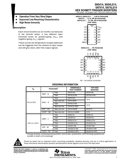
InputV T OutputPACKAGING INFORMATIONOrderable Device Status(1)PackageType PackageDrawingPins PackageQtyEco Plan(2)Lead/Ball Finish MSL Peak Temp(3)5962-9665801Q2A ACTIVE LCCC FK201TBD Call TI Level-NC-NC-NC 5962-9665801QCA ACTIVE CDIP J141TBD Call TI Level-NC-NC-NC 5962-9665801QDA ACTIVE CFP W141TBD Call TI Level-NC-NC-NC 5962-9665801VCA ACTIVE CDIP J141TBD Call TI Level-NC-NC-NC 5962-9665801VDA ACTIVE CFP W141TBD Call TI Level-NC-NC-NC JM38510/31302BCA ACTIVE CDIP J141TBD Call TI Level-NC-NC-NC SN5414J ACTIVE CDIP J141TBD Call TI Level-NC-NC-NC SN54LS14J ACTIVE CDIP J141TBD Call TI Level-NC-NC-NCSN7414D ACTIVE SOIC D1450Pb-Free(RoHS)CU NIPDAU Level-2-260C-1YEAR/Level-1-235C-UNLIMSN7414DE4ACTIVE SOIC D1450Pb-Free(RoHS)CU NIPDAU Level-2-260C-1YEAR/Level-1-235C-UNLIMSN7414DR ACTIVE SOIC D142500Pb-Free(RoHS)CU NIPDAU Level-2-260C-1YEAR/Level-1-235C-UNLIMSN7414DRE4ACTIVE SOIC D142500Pb-Free(RoHS)CU NIPDAU Level-2-260C-1YEAR/Level-1-235C-UNLIMSN7414N ACTIVE PDIP N1425Pb-Free(RoHS)CU NIPDAU Level-NC-NC-NC SN7414N3OBSOLETE PDIP N14TBD Call TI Call TISN7414NSR ACTIVE SO NS142000Pb-Free(RoHS)CU NIPDAU Level-2-260C-1YEAR/Level-1-235C-UNLIMSN7414NSRE4ACTIVE SO NS142000Pb-Free(RoHS)CU NIPDAU Level-2-260C-1YEAR/Level-1-235C-UNLIMSN74LS14D ACTIVE SOIC D1450Pb-Free(RoHS)CU NIPDAU Level-2-260C-1YEAR/Level-1-235C-UNLIMSN74LS14DBR ACTIVE SSOP DB142000Pb-Free(RoHS)CU NIPDAU Level-2-260C-1YEAR/Level-1-235C-UNLIMSN74LS14DBRE4ACTIVE SSOP DB142000Pb-Free(RoHS)CU NIPDAU Level-2-260C-1YEAR/Level-1-235C-UNLIMSN74LS14DR ACTIVE SOIC D142500Pb-Free(RoHS)CU NIPDAU Level-2-260C-1YEAR/Level-1-235C-UNLIMSN74LS14N ACTIVE PDIP N1425Pb-Free(RoHS)CU NIPDAU Level-NC-NC-NC SN74LS14N3OBSOLETE PDIP N14TBD Call TI Call TISN74LS14NE4ACTIVE PDIP N1425TBD Call TI Call TISN74LS14NSRG4ACTIVE SO NS142000Green(RoHS&no Sb/Br)CU NIPDAU Level-1-260C-UNLIM SNJ5414J ACTIVE CDIP J141TBD Call TI Level-NC-NC-NCSNJ5414W ACTIVE CFP W141TBD Call TI Level-NC-NC-NC SNJ54LS14FK ACTIVE LCCC FK201TBD Call TI Level-NC-NC-NC SNJ54LS14J ACTIVE CDIP J141TBD Call TI Level-NC-NC-NC SNJ54LS14W ACTIVE CFP W141TBD Call TI Level-NC-NC-NC (1)The marketing status values are defined as follows:ACTIVE:Product device recommended for new designs.LIFEBUY:TI has announced that the device will be discontinued,and a lifetime-buy period is in effect.NRND:Not recommended for new designs.Device is in production to support existing customers,but TI does not recommend using this part in a new design.PREVIEW:Device has been announced but is not in production.Samples may or may not be available.OBSOLETE:TI has discontinued the production of the device.(2)Eco Plan-The planned eco-friendly classification:Pb-Free(RoHS)or Green(RoHS&no Sb/Br)-please check /productcontent for the latest availability information and additional product content details.TBD:The Pb-Free/Green conversion plan has not been defined.Pb-Free(RoHS):TI's terms"Lead-Free"or"Pb-Free"mean semiconductor products that are compatible with the current RoHS requirements for all6substances,including the requirement that lead not exceed0.1%by weight in homogeneous materials.Where designed to be soldered at high temperatures,TI Pb-Free products are suitable for use in specified lead-free processes.Green(RoHS&no Sb/Br):TI defines"Green"to mean Pb-Free(RoHS compatible),and free of Bromine(Br)and Antimony(Sb)based flame retardants(Br or Sb do not exceed0.1%by weight in homogeneous material)(3)MSL,Peak Temp.--The Moisture Sensitivity Level rating according to the JEDEC industry standard classifications,and peak solder temperature.Important Information and Disclaimer:The information provided on this page represents TI's knowledge and belief as of the date that it is provided.TI bases its knowledge and belief on information provided by third parties,and makes no representation or warranty as to the accuracy of such information.Efforts are underway to better integrate information from third parties.TI has taken and continues to take reasonable steps to provide representative and accurate information but may not have conducted destructive testing or chemical analysis on incoming materials and chemicals.TI and TI suppliers consider certain information to be proprietary,and thus CAS numbers and other limited information may not be available for release.In no event shall TI's liability arising out of such information exceed the total purchase price of the TI part(s)at issue in this document sold by TI to Customer on an annual basis.元器件交易网IMPORTANT NOTICETexas Instruments Incorporated and its subsidiaries (TI) reserve the right to make corrections, modifications,enhancements, improvements, and other changes to its products and services at any time and to discontinueany product or service without notice. Customers should obtain the latest relevant information before placingorders and should verify that such information is current and complete. All products are sold subject to TI’s termsand conditions of sale supplied at the time of order acknowledgment.TI warrants performance of its hardware products to the specifications applicable at the time of sale inaccordance with TI’s standard warranty. T esting and other quality control techniques are used to the extent TIdeems necessary to support this warranty. Except where mandated by government requirements, testing of allparameters of each product is not necessarily performed.TI assumes no liability for applications assistance or customer product design. Customers are responsible fortheir products and applications using TI components. T o minimize the risks associated with customer productsand applications, customers should provide adequate design and operating safeguards.TI does not warrant or represent that any license, either express or implied, is granted under any TI patent right,copyright, mask work right, or other TI intellectual property right relating to any combination, machine, or processin which TI products or services are used. Information published by TI regarding third-party products or servicesdoes not constitute a license from TI to use such products or services or a warranty or endorsement thereof.Use of such information may require a license from a third party under the patents or other intellectual propertyof the third party, or a license from TI under the patents or other intellectual property of TI.Reproduction of information in TI data books or data sheets is permissible only if reproduction is withoutalteration and is accompanied by all associated warranties, conditions, limitations, and notices. Reproductionof this information with alteration is an unfair and deceptive business practice. TI is not responsible or liable forsuch altered documentation.Resale of TI products or services with statements different from or beyond the parameters stated by TI for thatproduct or service voids all express and any implied warranties for the associated TI product or service andis an unfair and deceptive business practice. TI is not responsible or liable for any such statements.Following are URLs where you can obtain information on other Texas Instruments products and applicationsolutions:Products ApplicationsAmplifiers Audio /audioData Converters Automotive /automotiveDSP Broadband /broadbandInterface Digital Control /digitalcontrolLogic Military /militaryPower Mgmt Optical Networking /opticalnetworkMicrocontrollers Security /securityTelephony /telephonyVideo & Imaging /videoWireless /wirelessMailing Address:Texas InstrumentsPost Office Box 655303 Dallas, Texas 75265Copyright 2005, Texas Instruments Incorporated。
5962-9954401HXC中文资料
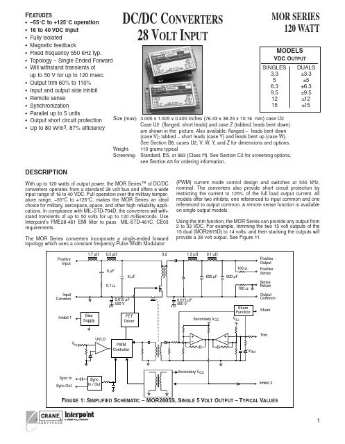
MOR SERIES 120 WATTDC/DC C ONVERTERS 28 V OLT I NPUT+_F EATURES•–55°C to +125°C operation •16 to 40 VDC input •Fully isolated•Magnetic feedback•Fixed frequency 550 kHz typ.••Will withstand transients of up to 50 V for up to 120 msec.•Output trim 60% to 110%•Input and output side inhibit •Remote sense •Synchronization•Parallel up to 5 units•Output short circuit protection•Up to 80 W/in 3, 87% efficiency DESCRIPTIONWith up to 120 watts of output power, the MOR Series™of DC/DC converters operates from a standard 28 volt bus and offers a wide input range of 16 to 40 VDC. Full operation over the military temper-ature range, –55°C to +125°C, makes the MOR Series an ideal choice for military, aerospace, space, and other high reliability appli-cations. In compliance with MIL-STD-704D, the converters will with-stand transients of up to 50 volts for up to 120 milliseconds. Use Interpoint’s FME 28-461 E MI filter to pass MIL-STD-461C, CE 03requirements.The MOR Series converters incorporate a single-ended forward topology which uses a constant frequency Pulse Width Modulator(PWM) current mode control design and switches at 550 kHz,nominal. The converters also provide short circuit protection by restricting the current to 125% of the full load output current. All models offer two inhibits, one referenced to input common and one referenced to output common. A remote sense function is available on single output models.Using the trim function, the MOR Series can provide any output from 2 to 33 VDC. For example, trimming the two 15 volt outputs of the 15 dual (MOR2815D) to 14 volts, and then stacking the outputs will provide a 28 volt output. See Figure 11.元器件交易网TYPICAL CHARACTERISTICSSYNC AND INHIBIT (INH1,INH2)PINS NOT IN USERECOMMENDED OPERATING CONDITIONSABSOLUTE MAXIMUM RATINGSInput Voltage Range•16 to 40 VDC continuous •50 V for 120 msec transient Case Operating Temperature (Tc)•–55°C to +125°C full power •–55°C to +135°C absolute Derating Output Power/Current•Linearly from 100% at 125°C to 0% at 135°C2MOR SERIES 120 WATTDC/DC CONVERTERSInput Voltage •16 to 40 VDCPower Dissipation (Pd)•30 WOutput Power•66 to 120 watts depending on modelLead Soldering Temperature (10 sec per lead)•300°CStorage Temperature Range (Case)•–65°C to +150°COutput Voltage Temperature Coefficient •100 ppm/°C typicalInput to Output Capacitance •150 pF typicalUndervoltage Lockout •15.5 V input typical Current Limit•125% of full load typical Isolation•100 megohm minimum at 500 V Audio Rejection •40 dB typicalConversion Frequency•Free run mode 550 kHz typical460 kHz. min, 570 kHz max • External sync range 525 to 625 kHz Inhibit Pin Voltage (unit enabled)• INH1 = 13 V typ, INH2 = 8 V typNotes: See notes 1, 2, 3, and 4 on the following page.SINGLE OUTPUT MODELS MOR283R3S MOR2805S MOR286R3S MOR289R5S PARAMETER CONDITION MIN TYP MAX MIN TYP MAX MIN TYP MAX MIN TYP MAX UNITS OUTPUT VOLTAGE 3.25 3.30 3.35 4.95 5.00 5.05 6.24 6.30 6.369.409.509.60VDC OUTPUT CURRENT V IN = 16 to 40 VDC 0—200—200—160—11A OUTPUT POWER V IN = 16 to 40 VDC 0—660—1000—1000—105WOUTPUT RIPPLE 10 kHz - 20 MHz VOLTAGETc = –55°C to +125°C —3080—3080—75100—75120mV p-p10 kHz - 2 MHz Tc = –55°C to +125°C —2050—2050—5060—5080LINE REGULATION V IN = 16 to 40 VDC —020—020—020—020mV LOAD REGULATION NO LOAD TO FULL —020—020—020—020mV INPUT VOLTAGE CONTINUOUS 162840162840162840162840VDC TRANSIENT 120 ms——50——50——50——50V INPUT CURRENTNO LOAD —70130—70130—70130—70130mA FULL LOAD —— 3.2—— 4.67—— 4.45—— 4.63A INHIBITED - INH1——10——10——10——10mAINHIBITED - INH2——70——70——70——70INPUT RIPPLE 10 kHz - 20 MHz CURRENT Tc = –55°C to +125°C —4090—50130—50100—50130mA pp EFFICIENCY 7478—7881—8183—8184—%LOAD FAULT 1POWER DISSIPATIONOVERLOAD ——27——30——30——30W SHORT CIRCUIT 2——22——27——24——24RECOVERY ——10——10——10——10msOUTPUT CURRENTTRIP POINT ——25——25——20——14ASHORT CIRCUIT 2——24——24——19——13STEP LOAD RESP .50% – 100% – 50%TRANSIENT ——250——250——500——500mV pk RECOVERY 3——200——200——300——300µs STEP LINE RESP .16 – 40 – 16 VDC TRANSIENT 4——400——400——500——500mV pk RECOVERY 3——300——300——300——300µs START-UPDELAY ——10——10——10——10ms OVERSHOOT —025—050—050—050mV pk INHIBIT PIN CURRENTUNIT INHIBITED—0.11.0—0.11.0—0.11.0—0.11.0mASync In (525 to 625 kHz)•Logic low 0.8 V max, duty cycle 15% to 50%•Logic high 4.5 V min, 9 V max •Referenced to input commonSync Out - Referenced to input common Inhibit (INH1,INH2) :TTL Open Collector •Logic low (output disabled), V = 0.2 V max.•INH1 referenced to input common •INH2 referenced to output common•Logic high (output enabled) open collectorTrim CaseInhibit (INH1,INH2) Sync Out Sync In ShareSense LinesNo connectionUsers discrimination No connection No connectionConnect to input common No connectionMust be connected to appropriate outputsElectrical Characteristics:25°C Tc,28 VDC Vin,100% load,free run,unless otherwise specified.元器件交易网3MOR SERIES 120 WATTDC/DC CONVERTERSSINGLE AND DUAL OUTPUT MODELSMOR2812S MOR2815S MOR283R3D MOR2805D PARAMETER CONDITIONSMIN TYP MAX MIN TYP MAX MIN TYP MAX MINTYP MAXUNITS OUTPUT VOLTAGE 5+V OUT 11.8812.0012.1214.8515.0015.153.25 3.30 3.354.955.00 5.05VDC –V OUT—————— 3.22 3.30 3.38 4.92 5.00 5.08OUTPUT CURRENT V IN = 16 to 40 VDC 0—9.20—8—±10206—±10206A OUTPUT POWER V IN = 16 to 40 VDC ——110——120——666——1006WOUTPUT RIPPLE 10 kHz -20 MHz VOLTAGETc = –55°C to +125°C — 75120—75150—5080—5080mV p-p+V OUT , ±V OUT 10 kHz -2 MHz Tc = –55°C to +125°C—50100—50120—3550—3550LINE REGULATION +V OUT—020—020—2550—2550mV V IN = 16 to 40 VDC –V OUT ———————50100—50100LOAD REGULATION +V OUT —020—020—2550—2550mV –V OUT ———————50150—50150CROSS REGULATION 7NEGATIVE V OUT ———————610—58%INPUT VOLTAGE CONTINUOUS 162840162840162840162840VDC TRANSIENT 120 msec——50——50——50——50V INPUT CURRENTNO LOAD —70130—70130—70140—70140mA FULL LOAD —— 4.72—— 5.10—— 3.2—— 4.67A INHIBITED - INH1——10——10——10——10mAINHIBITED - INH2——70——70——70——70INPUT RIPPLE 10 kHz - 20 MHz CURRENT Tc = –55°C to +125°C —50130—50130—60130—60130mA p-p EFFICIENCY 8486—8487—7677—7881—%LOAD FAULT 1POWER DISSIPATIONOVERLOAD ——30——30——27——30W SHORT CIRCUIT 2——22——22——22——27RECOVERY ——10——10——10——10msOUTPUT CURRENTTRIP POINT ——12——10——25——25ASHORT CIRCUIT 2——11——9——24——24STEP LOAD RESP .50% – 100% — 50%+V OUT , ±V OUT TRANSIENT ——600——600——250——250mV pk RECOVERY 3——300——300——200——200µs STEP LINE RESP .16 – 40 – 16 VDC +V OUT , ±V OUT TRANSIENT 4——600——600——400——400mV pk RECOVERY 3——300——300——300——300µs START-UPDELAY ——10——10——10——10ms OVERSHOOT ——50——50——25——50mV pk INHIBIT PIN CURRENTUNIT INHIBITED—0.11.0—0.11.0—0.11.0—0.11.0mANotes:1.Load fault conditions are measured with a resistive load.2.Short circuit is measured with a 10 m W (±10%) load.3.Time to settle to within 1% of Vout.4.Transition time > 10 µs5.Output voltage for dual output models is measured at half load.6.The maximum specification is the total output current/power. Up to 70% of that total is available from either output provided the other output maintains a minimum of 15% the total power used.7.Cross regulation percentages are for the following conditions:+Po = 30% and –Po = 70%+Po = 10% and –Po = 50%+Po = 70% and –Po = 30%+Po = 50% and –Po = 10%Electrical Characteristics:25°C Tc,28 VDC Vin,100% load,free run,unless otherwise specified.元器件交易网4MOR SERIES 120 WATTDC/DC CONVERTERSDUAL OUTPUT MODELSMOR286R3DMOR289R5D MOR2812D MOR2815D PARAMETER CONDITIONSMIN TYP MAX MIN TYP MAX MINTYP MAXMINTYP MAXUNITS OUTPUT VOLTAGE 5+V OUT 6.24 6.30 6.369.409.509.6011.8812.0012.1214.8515.0015.15VDC –V OUT6.20 6.30 6.409.359.509.6511.8012.0012.2014.7615.0015.24OUTPUT CURRENT 6V IN = 16 to 40 VDC —±816—±5.5311.05—±4.589.16—±4.008.00A 6OUTPUT POWER V IN = 16 to 40 VDC ——100——105——110——120WOUTPUT RIPPLE 10 kHz -20 MHz VOLTAGETc = –55°C to +125°C — 50100—75120—75120—75150mV p-p+V OUT / –V OUT 10 kHz -2 MHz Tc = –55°C to +125°C—3060—5080—50100—50120LINE REGULATION +V OUT —2550—2550—2550—2550mV V IN = 16 to 40 VDC –V OUT —50160—50100—50100—50100LOAD REGULATION +V OUT —2550—2550—2550—2550mV –V OUT—50200—50200—50200—50200CROSS REGULATION 7NEGATIVE V OUT —58—47—35—24%INPUT VOLTAGE CONTINUOUS 162840162840162840162840VDC TRANSIENT 120 msec ——50——50——50——50V INPUT CURRENTNO LOAD —70140—70140—70140—70140mA FULL LOAD —— 4.45—— 4.63—— 4.72—— 5.10A INHIBITED - INH1——10——10——10——10mAINHIBITED - INH2——70——70——70——70INPUT RIPPLE 10 kHz - 20 MHz CURRENT Tc = –55°C to +125°C ——130——130——130——130mA p-p EFFICIENCY 8183—8284—8486—8587—%LOAD FAULT 1POWER DISSIPATIONOVERLOAD ——30——30——30——30W SHORT CIRCUIT 2——24——24——22——20RECOVERY ——10——10——10——10msOUTPUT CURRENTTRIP POINT ——20——14——11——10ASHORT CIRCUIT 2——19——13——10——9STEP LOAD RESP .50% – 100% — 50%±V OUTTRANSIENT ——500——500——600——600mV pk RECOVERY 3——300——300——300——300µs STEP LINE RESP .16 – 40 – 16 VDC ±V OUT TRANSIENT 4——500——600——600——750mV pk RECOVERY 3——300——300——300——300µs START-UPTIME ——10——10——10——10ms OVERSHOOT ——50——50——50——50mV pk INHIBIT PIN CURRENTUNIT INHIBITED—0.11.0—0.11.0—0.11.0—0.11.0mAElectrical Characteristics:Tc = 25°C,full load,Vin = 28 VDC,free run,unless otherwise specified.Notes:1.Load fault conditions are measured with a resistive load.2.Short circuit is measured with a 10 m W (±10%) load.3.Time to settle to within 1% of Vout.4.Transition time > 10 µs5.Output voltage for dual output models is measured at half load.6.The maximum specification is the total output current/power. Up to 70% of that total is available from either output provided the other output maintains a minimum of 15% the total power used.7.Cross regulation percentages are for the following conditions:+Po = 30% and –Po = 70%+Po = 10% and –Po = 50%+Po = 70% and –Po = 30%+Po = 50% and –Po = 10%元器件交易网PIN DESCRIPTIONS AND FUNCTIONSP IN O UTP OSITIVE I NPUT AND I NPUT C OMMONSteady state voltage range is 16 to 40 VDC. Transient range is 40 to 50 V for a maximum of 120 msec. Low voltage lockout prevents the units from operating below approximately 15.5 VDC input voltage to keep system current levels smooth, especially during initialization or re-start operations. All models include a soft-start function to prevent large current draw and minimize overshoot.C ASE ANDE XTERNAL I NPUTF ILTERSInternal 500 V capacitors are connected between the case and input common and between the case and output common. See Figure 1.Interpoint’s FME filters are recommended to meet CE03 require-ments for reflected input line current. When using an external input filter it is important that the case of the filter and the case of the converter be connected through as low as an impedance as possible. Direct connection of the baseplates to chassis ground is the best connection. If connected by a single trace, the trace should be as wide as it is long. T RIMBoth single and dual outputmodels include a trim function.Output voltage can be trimmedfrom 60% up to 110% of nominalV out . When trimming up, do notexceed the maximum outputpower. When trimming down, donot exceed the maximum outputcurrent.On dual models the positiveoutput is regulated and thenegative output is transformercoupled (cross-regulated) to thepositive output. When trimmingthe duals, both output voltageswill be adjusted equally.I NHIBIT1 AND2Two inhibit terminals disable switching, resulting in no output and very low quiescent input current. The two inhibit pins allow access to an inhibit function on either side of the isolation barrier to help maintain isolation.An open collector isrequired for inter-facing with both ofthe inhibit pins.Applying an open-collector TTL logiclow to either inhibitpin will inhibit theconverter. Applyingan open collectorTTL logic high orleaving the pinsopen will enable the converter. Inhibit 1 is referenced to Input Common, while Inhibit 2 is referenced to Sense Return on the output side.The open circuitvoltage for Inhibit 1 is13 V and for Inhibit 2 itis 8 V. Float the inhibitpin(s) if not used. Therequired logic lowvoltage level is 0.2 Vmaximum.5MOR SERIES120 WATTDC/DC CONVERTERS元器件交易网6MOR SERIES 120 WATTDC/DC CONVERTERSS YNC I N AND S YNC O UTThe MOR converters can be synchronized to the system clock by applying a TTL compat-ible sync signal to the Sync In pin. Sync Out can be used to synchro-nize other components to the MOR converter ’s switching frequency.The frequency range for external synchronization is 525 to 625 kHz.The requirements for an external signal are 15% to 50% duty cycle,0 ≤L ≤0.8 V and 4.5 ≤H ≤9 V.Both Sync In and Sync Out are referenced to input common. Sync In should be grounded to input common if not used.P OSITIVE S ENSE ,S ENSE R ETURNA special remote sensing feature maintains the desired output voltage at the load. When this feature is not used, connect the sense lines to their respective output terminals. Remote sensing is available on single output models only. See Figure 12. Do not exceed 110% of Vout and maximum output power.S HARE (P ARALLELING )By using the Share pin, up to five single or dual converters may be paralleled for a total output power of over 500 watts (90% Pout /converter, max.). The converters will share within 10% of each other at 25 to 90% rated power. MOR converters feature true n+1redundancy for reliability in critical applications. See Figure 9 for the proper connections.All Positive Outputs and Positive Senses should be connected to a common point. All Negative Outputs and Sense Returns should be connected to a common point. The Share pin is referenced to Sense Return. Leave the share pin floating (unconnected) if not used.P OSITIVE O UTPUT ,N EGATIVE O UTPUT AND O UTPUT C OMMONOutput current is limited to 125% of maximum specified current under short circuit or load fault conditions.Single output models operate from no load to full load. Dual output models with balanced loads operate from no load to full load. For dual models with unbalanced loads, at least 10% of the total output power must be drawn from the positive outputat all times, however, the negative output does not require a minimum load.See note 7, cross regula-tion, under the E lectrical Characteristics Tables.Dual outputs may be“stacked ” to double the output voltage.T YPICAL C ONNECTIONS元器件交易网7MOR SERIES 120 WATTDC/DC C ONVERTERS元器件交易网8MOR SERIES 120 WATTDC/DC CONVERTERSIGUREF IGURE 29FIGURE 30F IGURE 31MOR2812D Sync Out200V /d i v500 ns/divMOR2805S Output Ripple (Vout)20 m V /d i vMOR2805S Input Ripple Current (Iin)20 m A /d i v1 µs/div25 µs/divRepresentative of all models80% LoadTypical Performance Curves:25°C Tc ,28 VDC Vin,100% load,20 MHz BW,free run,unless otherwise specified.元器件交易网9MOR SERIES 120 WATTDC/DC CONVERTERSF IGURE 38F IGURE 39F IGURE 40F IGURE 41F IGURE 42F IGURE43MOR2815S Step Load Response100 -50%Step Load200 m V /d i v100 µs/div50 - 100%Step LoadMOR2815S Step Line Response50 µs/divVoutVinVoutVinV i n 10 V /d i vV o u t 50 m V /d i vMOR2815S Turn On Response2.5 ms/divVinVout20 V /d i v5 V /d i vMOR2805D Output Ripple (±Vout)20 m V /d i v1 µs/div+Vout–VoutMOR2805D Input Ripple (Iin)20 m A /d i v1 µs/div 25 µs/divMOR2805D Step Load Response100 - 50%Step Load50 m V /d i v50 µs/div50% Load +Vout–Vout18 to 40 V, 40 to 18 V, 50% loadAll combinations of line and load80% load each output80% load each outputTypical Performance Curves:25°C Tc ,28 VDC Vin,100% load,20 MHz BW,free run,unless otherwise specified.F IGURE 35F IGURE 36F IGURE 37F IGURE 32F IGURE 33F IGURE 34MOR2805S Step Load Response100 -50%Step Load100 m V /d i v100 µs/divMOR2805S Step Line ResponseMOR2805S Turn On ResponseVoutVinVinVoutMOR2805S Inhibit Release Inrush Current 5 ms/div50 - 100%Step LoadVoutVinV i n 10 V /d i vV o u t 50 m V /d i v10 V /d i v2 V /d i vIinVout2 A /d i v2 V /d i vMOR2815S Output Ripple (Vout)20 m V /d i v1 µs/divMOR2815S Input Ripple (Iin)20 m A /d i v18 to 40 V, 40 to 18 VAll combinations of line and loadWith and without 470 µF cap. load元器件交易网10MOR SERIES 120 WATTDC/DC C ONVERTERSF IGURE 50F IGURE 51F IGURE 52F IGURE 53F IGURE 54MOR2812D Step Load Response100 - 50%Step Load100 m V /d i v100 µs/div50% Load+Vout –VoutMOR2812D Step Load Response50 - 100%Step Load100 m V /d i v50% Load+Vout–VoutMOR2812D Step Line Response100 µs/div+VoutVin+VoutVinV i n 10 V /d i vV o u t 100 m V /d i vMOR2812D Turn On Response2.5 ms/divVin+Vout20 V /d i v5 V /d i v–VoutMOR2812D Inhibit Release Inrush CurrentIinVout2 A /d i v 5 V /d i v18 to 40 V, 40 to 18 VTypical Performance Curves:25°C Tc ,28 VDC Vin,100% load,20 MHz BW,free run,unless otherwise specified.VinF IGURE 44F IGURE 45F IGURE 46F IGURE 47F IGURE 48F IGURE 49MOR2805D Step Load Response50 - 100%Load50 m V /d i v50 µs/div50% Load+Vout–VoutMOR2805D Step Line Response25 µs/div–VoutVin+VoutMOR2805D Step Line Response–Vout+Vout MOR2805D Turn On Response2.5 ms/divVin+Vout20 V /d i v2 V /d i v–VoutMOR2812D Output Ripple (±Vout)20 m V /d i v+Vout–VoutMOR2812D Input Ripple (Iin)20 m A /d i v1 µs/div 25 µs/div V i n 20 V /d i vV o u t 100 m V /d i vV in 20 V /d i vV o u t 100 m V /d i v 80% load each output18 to 40 V, 80% load each output40 to 18 V, 80% load each output元器件交易网1112120 WATT1314120 WATT1516120 WATTTEST125°C 125°C STANDARD/ES /883 (Class H)*PRE-CAP INSPECTION 25°C Method 2017,2032yesyesyesTEMPERATURE CYCLE (10 times)Method 1010, Cond. C, -65°C to 150°C no no yes Method 1010, Cond. B, -55°C to 125°C no yes noCONSTANT ACCELERATION 25°C Method 2001, 3000 g no no yes Method 2001, 500 gno yes noBURN-INMethod 1015, 160 hours at 125°C no no yes 96 hours at 125°C case (typical)no yes noFINAL ELECTRICAL TEST MIL-PRF-38534, Group A Subgroups 1 through 6: -55°C, +25°C, +125°C no no yes Subgroups 1 and 4: +25°C case yes yes noHERMETICITY TESTING 25°C Fine Leak, Method 1014, Cond. A no yes yes Gross Leak, Method 1014, Cond. C no yes yes Gross Leak, Dip (1 x 10⁻³)yes no noFINAL VISUAL INSPECTION 25°C Method 2009yes yes yesTest methods are referenced to MIL-STD-883 as determined by MIL-PRF-38534.E NVIRONMENTAL S CREENING20420-001-DTS RevD. This revision supercedes all previous releases.All technical information is believed to be accurate, but no responsibility is assumed for errors or omissions. Interpoint reserves the right to make changes in products or specifications without notice. MOR Series is a trademark of Interpoint. Copyright ©1999-2003 Interpoint. All rights reserved.Contact Information:Interpoint Headquarters USA Phone:1-800-822-8782+425-882-3100Email:power@ Interpoint UKPhone:+44-1252-872266Email:poweruk@Interpoint FrancePhone:+33-134285455Email:powerfr@。
5962F8957701VXXA资料
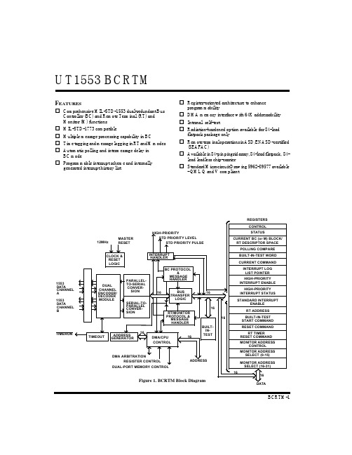
BCRTM-1UT1553 BCRTMF EATURESp Comprehensive MIL-STD-1553 dual-redundant BusController (BC) and Remote Terminal (RT) and Monitor (M) functions p MIL-STD-1773 compatiblep Multiple message processing capability in BCp Time tagging and message logging in RT and M modes p Automatic polling and intermessage delay in BC modepProgrammable interrupt scheme and internally generated interrupt history listp Register-oriented architecture to enhanceprogrammabilityp DMA memory interface with 64K addressability p Internal self-testp Radiation-hardened option available for 84-leadflatpack package onlyp Remote terminal operations in ASD/ENASD-certified(SEAFAC)p Available in 84-pin pingrid array, 84-lead flatpack, 84-lead leadless chip-carrierp Standard Microcircuit Drawing 5962-89577 available- QML Q and V compliant161616CONTROLDMA/CPU MESSAGE RT/MONITOR MESSAGE BC PROTOCOLHANDLERINTERRUPT CONVER-PARALLEL SERIAL-TO- CONVER-TO-SERIAL PARALLEL-MODULEDECODER ENCODER/CHANNEL DUAL BUS TRANSFER LOGICADDRESS16TIMEOUTTIMERONCLOCK &RESET 12MHzMASTER RESETGENERATORADDRESS 161553HIGH-PRIORITY RT ADDRESS STANDARD INTERRUPTHIGH-PRIORITY INTERRUPT LOG CURRENT COMMAND BUILT-IN-TEST WORD POLLING COMPARECURRENT BC (or M) BLOCK/STATUSCONTROLREGISTERS LIST POINTER DATA16BUILT-IN-TEST1616MONITOR ADDRESSINTERRUPT STATUS INTERRUPT ENABLESION SIONPROTOCOL &HANDLER&HANDLERDATACHANNEL B1553DATACHANNEL ALOGICHIGH-PRIORITYSTD PRIORITY LEVELSTD PRIORITY PULSE DMA ARBITRATIONREGISTER CONTROLDUAL-PORT MEMORY CONTROLRT DESCRIPTOR SPACEENABLEBUILT-IN-TEST START COMMAND RESET COMMAND CONTROL MONITOR ADDRESSSELECT (0-15)MONITOR ADDRESS Figure 1. BCRTM Block DiagramSELECT (16-31)RT TIMERRESET COMMANDTable of Contents1.0INTRODUCTION. . . . . . . . . . . . . . . . . . . . . . . . . . . . . . . . . . . . . . . . . . . . . . . . . . . . . . . . . . . . 31.1 Features - Remote Terminal (RT) Mode. . . . . . . . . . . . . . . . . . . . . . . . . . . . . . .31.2 Features - Bus Controller (BC) Mode. . . . . . . . . . . . . . . . . . . . . . . . . . . . . . . . .31.3Features - Monitor (M) Mode. . . . . . . . . . . . . . . . . . . . . . . . . . . . . . . . . . . . . . .42.0 PIN IDENTIFICATION AND DESCRIPTION. . . . . . . . . . . . . . . . . . . . . . . . . . . . . . . . . . . . 53.0 INTERNAL REGISTERS . . . . . . . . . . . . . . . . . . . . . . . . . . . . . . . . . . . . . . . . . . . . . . . . . . . . 124.0 SYSTEM OVERVIEW. . . . . . . . . . . . . . . . . . . . . . . . . . . . . . . . . . . . . . . . . . . . . . . . . . . . . . . 205.0 SYSTEM INTERFACE. . . . . . . . . . . . . . . . . . . . . . . . . . . . . . . . . . . . . . . . . . . . . . . . . . . . . . . 205.1 DMA Transfers. . . . . . . . . . . . . . . . . . . . . . . . . . . . . . . . . . . . . . . . . . . . . . . . .205.2 Hardware Interface . . . . . . . . . . . . . . . . . . . . . . . . . . . . . . . . . . . . . . . . . . . . . .215.3 CPU Interconnection. . . . . . . . . . . . . . . . . . . . . . . . . . . . . . . . . . . . . . . . . . . . .215.4 RAM Interface. . . . . . . . . . . . . . . . . . . . . . . . . . . . . . . . . . . . . . . . . . . . . . . . .235.6 Transmitter/Receiver Interface . . . . . . . . . . . . . . . . . . . . . . . . . . . . . . . . . . . . .236.0 REMOTE TERMINAL ARCHITECTURE. . . . . . . . . . . . . . . . . . . . . . . . . . . . . . . . . . . . . . 236.1 RT Functional Operation. . . . . . . . . . . . . . . . . . . . . . . . . . . . . . . . . . . . . . . . . .246.1.1 RT Subaddress Descriptor Definitions. . . . . . . . . . . . . . . . . . . . . . . . . .246.1.2Message Status Word . . . . . . . . . . . . . . . . . . . . . . . . . . . . . . . . . . . . . . .256.1.3 Mode Code Descriptor Definition . . . . . . . . . . . . . . . . . . . . . . . . . . . . .266.2 RT Error Detection . . . . . . . . . . . . . . . . . . . . . . . . . . . . . . . . . . . . . . . . . . . . . .286.3 RT Operational Sequence . . . . . . . . . . . . . . . . . . . . . . . . . . . . . . . . . . . . . . . . .287.0 BUS CONTROLLER ARCHITECTURE . . . . . . . . . . . . . . . . . . . . . . . . . . . . . . . . . . . . . . . 297.1 BC Functional Operation . . . . . . . . . . . . . . . . . . . . . . . . . . . . . . . . . . . . . . . . .307.2 Polling. . . . . . .. . . . . . . . . . . . . . . . . . . . . . . . . . . . . . . . . . . . . . . . . . . . . . . . .317.3 BC Error Detection. . . . . . . . . . . . . . . . . . . . . . . . . . . . . . . . . . . . . . . . . . . . . .317.4 BC Operational Sequence. . . . . . . . . . . . . . . . . . . . . . . . . . . . . . . . . . . . . . . . .327.5BC Operational Example . . . . . . . . . . . . . . . . . . . . . . . . . . . . . . . . . . . . . . . . .338.0 MONITOR ARCHITECTURE . . . . . . . . . . . . . . . . . . . . . . . . . . . . . . . . . . . . . . . . . . . . . . . . 348.1Monitor Functional Operation. . . . . . . . . . . . . . . . . . . . . . . . . . . . . . . . . . . . . .358.2Monitor Error Detection . . . . . . . . . . . . . . . . . . . . . . . . . . . . . . . . . . . . . . . . . .358.3Monitor Operational Sequence. . . . . . . . . . . . . . . . . . . . . . . . . . . . . . . . . . . . .359.0 EXCEPTION HANDLING AND INTERRUPT LOGGING . . . . . . . . . . . . . . . . . . . . . . . . 3610.0 MAXIMUM AND RECOMMENDED OPERATING CONDITIONS . . . . . . . . . . . . . . . . 4011.0 DC ELECTRICAL CHARACTERISTICS . . . . . . . . . . . . . . . . . . . . . . . . . . . . . . . . . . . . . . 4112.0 AC ELECTRICAL CHARACTERISTICS . . . . . . . . . . . . . . . . . . . . . . . . . . . . . . . . . . . . . . 4213.0 PACKAGE OUTLINE DRAWINGS. . . . . . . . . . . . . . . . . . . . . . . . . . . . . . . . . . . . . . . . . . . . 51BCRTM-21.0 I NTRODUCTIONThe monolithic CMOS UT1553 BCRTM provides the system designer with an intelligent solution toMIL-STD-1553B multiplexed serial data bus design problems. The UT1553B BCRTM is a single-chip device that implements all three of defined MIL-STD-1553B functions - Bus Controller, Remote Terminal, and Monitor. Designed to reduce host CPU overhead, the BCRTM’s powerful state machines automatically execute message transfers, provide interrupts, and generate status information. Multiple registers offer many programmable functions as well as extensive information for host use. In the BC mode, the BCRTM uses a linked-list message scheme to provide the host with message chaining capability. The BCRTM enhances memory use by supporting variable-size, relocatable data blocks. In the RT mode, the BCRTM implements time-tagging and message history functions. It also supports multiple (up to 128) message buffering and variable length messages to any subaddress.In the Monitor (M) mode, the BCRTM’s powerful linked list command block structure allows it to process a series of monitored 1553 messages without the intervention of the host. The BCRTM can store as much bus traffic as can be contained in its 64K memory space. In addition, the host has the capability of instructing the BCRTM to monitor and store data for only selected remote terminals.The UT1553 BCRTM is an intelligent, versatile, and easy to implement device -- a powerful asset to system designers.1.1 Features - Remote Terminal (RT) ModeIndexingThe BCRTM is programmable to index or buffer messages on a subaddress-by-subaddress basis. The BCRTM, which can index as many as 128 messages, can also assert an interrupt when either the selected number of messages is reached or every time a specified subaddress is accessed. Variable Space AllocationThe BCRTM can use as little or as much memory (up to 64K) as needed.Selectable Data StorageAddress programmability within the BCRTM provides flexible data placement and convenient access. Sequential Data StorageThe BCRTM stores/retrieves, by subaddress, all messages in the order in which they are transacted.Sequential Message Status InformationThe BCRTM provides message validity, time-tag, and word-count information, and stores it sequentially in a separate, cross-referenced list.Illegalizing Mode Codes and SubaddressesThe host can declare mode codes and subaddresses illegal by setting the appropriate bit(s) in memory. Programmable Interrupt SelectionThe host CPU can select various events to cause an interrupt with provision for high and standard priority interrupts. Interrupt History ListThe BCRTM provides an Interrupt History List that records, in the order of occurrence, the events that caused the interrupts. The list length is programmable.1.2 Features - Bus Controller (BC) ModeMultiple Message ProcessingThe BCRTM autonomously processes any number of messages or lists of messages that may be stored in a 64K memory space.Automatic Intermessage DelayWhen programmed by the host, the BCRTM can delay a host-specified time before executing the next message in sequence.Automatic PollingWhen polling, the BCRTM interrogates the remote terminals and then compares their status word responses to the contents of the Polling Compare Register. The BCRTM can interrupt the host CPU if an erroneous remote terminal status word response occurs.Automatic RetryThe BCRTM can automatically retry a message on busy, message error, and/or response time-out conditions. The BCRTM can retry up to four times on the same or on the alternate bus.Programmable Interrupt SelectionThe host CPU can select various events to cause an interrupt with provision for high and standard priority interrupts. Interrupt History ListThe BCRTM provides an Interrupt History List that records, in the order of occurrence, the events that caused the interrupts. The list length is programmable.Variable Space AllocationThe BCRTM uses as little or as much memory (up to 64K) as needed.Selectable Data StorageAddress programmability within the BCRTM provides flexible data placement and convenient access.BCRTM-31.3 Features - Monitor (M) ModeCommand History ListThe BCRTM’s linked list command block structure permits the BCRTM to process a series of monitored messages without host intervention.Monitor Selected Terminal AddressThe host can select the remote terminals to be monitored by programming the proper bits in the Terminal Address Select registers (Registers16 and 17). The BCRTM can monitor any or all remote terminals.Variable Space AllocationThe BCRTM can use as little or as much memory (up to 64K) as needed Selectable Data StorageAddress programmability within the BCRTM provides flexible data placement and convenient access. Sequential Data StorageThe BCRTM stores, by Terminal Address, all 1553 messages in the order in which they are transacted. Programmable Interrupt SelectionThe host can select a wide variety of events that may cause an interrupting event.Interrupt History ListThe BCRTM stores, chronologically in memory, an Interrupt History List of each event that causes an interrupt.BCRTM-4BCRTM-5**Pin internally pulled up.+Pin at high impedance when not asserted ++Bidirectional pin.*Formerly MEMWIN.+++++++******LCC, flatpack pin number not in parentheses.() Pingrid array pin identification in parentheses.TAZ TAO RAZ RAO TBZ TBO RBZ RBO RTA0RTA1RTA2RTA3RTA4RTPTY CLK MCLK MCLKD2A0A1A2A3A4A5A6A7A8A9A10A11A12A13A14A15D0D1D2D3D4D5D6D7D8D9D10D11D12D13D14D1513(K3)14(L2)1718(L4)(K6)15161920(L3)(K5)(L5)(K4)28(K8) **29(L9) **30(L10) **31(K9) **32(L11) **68(A6)69(A4)70(B4)25(K7)26(J7)27(L8)72(A2)75(B2)33(K10) **73(B3)*56(A10)57(A9)67(B5)58(B8)61(B7)60(C7)53(A11)52(C10)59(A8)54(B10)62(A7)55(B9)66(A5)11(A3)74(K2)12(A1)10(J2)24(L7)34(J10)35(K11)3637383940414445464748495051(J11)(H10)(H11)(G9)(G10)(G11)(E9)(E11)(E10)(F11)(D11)(D10)(C11)(B11)987654328382818079787776(K1)(J1)(H2)(H1)(G3)(G2)(G1)(F1)(E1)(E2)(F2)(D1)(D2)(C1)(B1)(C2)234364*********(L6)(F9)(C6)(E3)(F3)(J6)(F10)(B6)2165(J5)(C5)71(L1)BIPHASE OUTBIPHASE INTERMINAL ADDRESSSTATUS SIGNALSDMASIGNALSCONTROLSIGNALSADDRESS LINESDATALINESPOWERGROUNDCLOCK SIGNALS+++++++2.0 P IN I DENTIFICATION A ND D ESCRIPTION+**STDINTL STDINTP HPINT TIMERON COMSTR SSYSF BCRTF CHA/B TEST DMAR DMAG DMAGO DMACK BURST TSCTLRD WR CS AEN BCRTSELLOCK MRST EXTOVRRRD RWR MEMCSI MEMCSOV DD V DD V DD V DD V SS V SS V SS V SS Figure 2. BCRT Functional Pin DescriptionA034B11TTB Bit 0 (LSB) of the Address busA1 A2 A3 A4 A5 A6 A7 A8 A9 A10 A11 A123536373839404144454647C11D10D11F11E10E11E9G11G10G9H11TTBTTBTTBBit 1 of the Address busBit 2 of the Address busBit 3 of the Address busBit 4 of the Address busBit 5 of the Address busBit 6 of the Address busBit 7 of the Address busBit 8 of the Address busBit 9 of the Address busBit 10 of the Address busBit 11 of the Address bus 48H10A13 A144950J11K11TTOTTOTTONAME PIN NUMBERLCC PGATYPE ACTIVE DESCRIPTIONA1551J10TTBTTOTTOTTOTTOTTOTTOTTOTTOBit 12 of the Address busBit 13 of the Address busBit 14 of the Address busBit 15 (MSB) of the Address bus--------------------------------Legend for TYPE and ACTIVE fields:TUI = TTL input (pull-up)AL = Active lowAH = Active highZL = Active low - inactive state is high impedanceTI = TTL inputTO = TTL outputTTO = Three-state TTL outputTTB = BidirectionalNotes:1. Address and data buses are in the high-impedance state when idle.2. Flatpack pin numbers are same as LCC.BCRTM-6BCRTM-7TTB TTB TTB TTB D0D1D2D39K1876J1H2H1Bit 0 (LSB) of the Data bus Bit 1 of the Data bus Bit 2 of the Data bus Bit 3 of the Data bus D4D5D6D7D8D9D10D11543283828180G3G2G1F1E1E2F2D1TTB TTB TTB TTB TTB TTB TTB TTB Bit 4 of the Data bus Bit 5 of the Data bus Bit 6 of the Data bus Bit 7 of the Data bus Bit 8 of the Data bus Bit 9 of the Data bus Bit 10 of the Data bus Bit 11 of the Data bus ------------------------NAMETYPE ACTIVE DESCRIPTIONDATA BUSD12D13D14D1579787776D2C1B1C2TTB TTB TTB TTBBit 12 of the Data bus Bit 13 of the Data bus Bit 14 of the Data bus Bit 15 (MSB) of the Data bus--------PIN NUMBER LCC PGANAMETYPE ACTIVE DESCRIPTIONRTA0TERMINAL ADDRESS INPUTS28K8TUI Remote Terminal Address Bit 0 (LSB). The entireRT address is strobed in at Master Reset. Verify it by reading the Remote Terminal Address Register.All the Remote Terminal Address bits are internally pulled up.RTA129L9TUI Remote Terminal Address Bit 1. This is bit 1 of the Remote Terminal Address.RTA230L10TUI Remote Terminal Address Bit 2. This is bit 2 of the Remote Terminal Address.RTA331K9TUI Remote Terminal Address Bit 3. This is bit 3 of the Remote Terminal Address.--------RTPTY33K10TUIRemote Terminal (Address) Parity. This is an odd parity input for the Remote Terminal Address.RTA432L11TUI Remote Terminal Address Bit 4. This is bit 4 (MSB) of the Remote Terminal Address.----PIN NUMBER LCC PGABCRTM-8626160A7B7C7TI TI TI AL AL AL AEN66A5TIAHBCRTSEL 11L1TUI --LOCK 1224K2L7TUI TUI AHAL10J2ALNAMETYPE ACTIVE DESCRIPTIONCONTROL SIGNALS5459B10A8TO TUI ALAL52C10TO AL53A11TO ALTI Read. The host uses this in conjunction with CS to read aninternal BCRTM register.Write. The host uses this in conjunction with CS to write to an internal BCRTM register.BC/RT Select. This selects between either the Bus Con-troller or Remote Terminal mode. The BC/RT Mode Select bit in the Control Register overrides this input if the LOCK pin is not high. This pin is internally pulled high.Lock. When set, this pin prevents internal changesto both the RT address and BC/RT mode select functions. This pin is internally pulled high.External Override. Use this in multi-redundant applica-tions. Upon receipt, the BCRTM aborts all current activ-ity. EXTOVR should be connected to COMSTR output of the adjacent BCRTM when used. This pin is internally pulled high.Memory Chip Select Out. This is the regenerated MEMCSI input for external RAM during the pseudo-dual-port RAM mode. The BCRTM also uses it to select external memory during memory accesses.RD WR CS EXTOVR MRSTMEMCSOMEMCSIRRD RWRMemory Chip Select In. Used in the pseudo-dual-port RAM mode only, MEMCSI is received from the host and is propagated through to the MEMCSO.RAM Read. In the pseudo-dual-port RAM mode, the host uses this signal in conjunction with MEMCSO to read from external RAM through the BCRTM. It is also the signal the BCRTM uses to read from memory. It isasserted following receipt of DMAG. When the BCRTM performs multiple reads, this signal is pulsed.RAM Write. In the pseudo-dual-port RAM mode, the CPU and BCRTM use this to write to external RAM. This signal is asserted following receipt of DMAG. For multi-ple writes, this signal is pulsed.PIN NUMBER LCC PGAChip Select. This selects the BCRTM when accessing the BCRTM’s internal register.Address Enable. The host CPU uses AEN to indicate to the BCRTM that the BCRTM’s address lines can be asserted; this is a precautionary signal provided to avoid address bus crash. If not used, it must be tied high.Master Reset. This resets all internal state machines, encoders, decoders, and registers. The minimum pulse width for a successful Master Reset is 500ns.BCRTM-9686970A6A4B4TTOTO TTOZLAL ZLNAME TYPE ACTIVE DESCRIPTION252627K7J7L8TO TO TO ALALSSYSF BCRTF TEST727573A2B2B3TI TO TOAHAHALSTATUS SIGNALS(RT)Timer On. This is a 760-microsecond fail-safe trans-mitter enable timer. Started at the beginning of a transmis-sion. TIMERON goes inactive 760 microseconds later or is reset automatically with the receipt of a new command. Use it in conjunction with CHA/B output to provide a fail safe timer for channel A and B transmitters.--Standard Interrupt Level. This is a level interrupt. It isasserted when one or more events enabled in either the Standard Interrupt Enable Register, RT Descriptor, or BC Command Block occur. Resetting the Standard Interrupt bit in the High-Priority Interrupt Status/Reset Register clears the interrupt.STDINTLSTDINTP Standard Interrupt Pulse. STDINTP pulses when an inter-rupt is logged.HPINTHigh Priority Interrupt. The High-Priority Interrupt level is asserted upon occurrence of events enabled in the High Priority Interrupt Enable Register. The corresponding bit(s) in the High-Priority Interrupt Status/Reset Register reset HPINT.TIMERONCOMSTR CHA/B Channel A/B. This indicates the active or last active channel.TEST. This pin is used as a factory test pin. (Formerly MEMWIN.)PIN NUMBER LCC PGA (RT) Command Strobe. The BCRTM asserts thissignal after receiving a valid command. The BCRTM deac-tivates it after servicing the command.Subsystem Fail. Upon receipt, this signal propagates directly to the RT 1553 status word and the BCRTM Status Register.BCRT Fail. this indicates a Built-In-Test (BIT) failure.In the RT mode, the Terminal Flag bit in 1553 status word is also set.NAMETYPE ACTIVE DESCRIPTIONBIPHASE INPUTSRAO 16K4TI RBO 20L5TI RAZRBZ 1519L3K5TITI --------PIN NUMBER LCC PGAReceive Channel A One. This is the Manchester-en-codedtrue signal input from Channel A of the bus receiver Receive Channel A Zero. This is Manchester-encoded complementary signal input from Channel A of the bus receiverReceive Channel B One. This is the Manchester-en-coded true signal input from Channel B of the bus receiver.Receive Channel B Zero. This is the Manchester-en-coded complementary signal input from Channel B of the bus receiverBCRTM-10NAMETYPE ACTIVE DESCRIPTIONTAO 14L2TO TAZ 13K3TO TBO 18K6TO ------TBZ 17L4TO --BIPHASE OUTPUTSTransmit Channel A One. This is the Manchester-encodedtrue output to be connected to the Channel A bus transmitter input. This signal is idle low.Transmit Channel A Zero. This is the Manchester-encoded complementary output to be connected to the Channel A bus transmitter input. This signal is idle low.Transmit Channel B One. This is the Manchester-encoded true output to be connected to the Channel B bus transmitter input. This signal is idle low.Transmit Channel B Zero. This is the Manchester-encoded complementary output to be connected to the Channel B bus transmitter input. This signal is idle low.PIN NUMBER LCC PGA56A10ZL576758A9B5B8ALAL ZLTTO TI TO TTONAME TYPE ACTIVE DESCRIPTIONDMA SIGNALS55B9TO ALBURST 74A1TO AHDMA Request. The BCRTM issues this signal when access toRAM is required. It goes inactive after receiving a DMAG signal.DMARDMAGDMAGO DMACKTSCTLDMA Grant Out. If DMAG is received but not needed, it passes through to this output.DMA Acknowledge. The BCRTM asserts this signal to confirm receipt of DMAG, it stays low until memory access is complete.PIN NUMBER LCC PGADMA Grant. This input to the BCRTM allows theBCRT to access RAM. It is recognized 45ns before the rising edge of MCLKD2.Three-State Control. This signal indicates when theBCRTM is actually accessing memory. The host subsystem’s address and data lines must be in the high-impedance state when the signals active. This signal assists in placing the external data and address buffers into the high-impedance state.Burst (DMA Cycle). This indicates that the currentDMA cycle transfers at least two words; worst case is five words plus a “dummy” word.BCRTM-11NAME TYPE ACTIVEDESCRIPTIONCLKMCLK MCLKD2216571J5C5A3TITI TO Memory Clock Divided by Two. This signal is the Memory Clock input divided by two. It assists the host subsystem in synchronizing DMA events.Clock. The 12MHz input clock requires a 50%± 10% duty cycle with an accuracy of ± 0.01%. The accuracy is required in order to meet the Manchester encoding/decoding requirements of MIL-STD-1553.Memory Clock. This is the input clock frequency the BCRTM uses for memory accesses. The memory cycle time is equal to two MCLK cycles. Therefore, RAM access time is dependent upon the chosen MCLK frequency (6MHzminimum, 12MHz maximum). Please see the BCRTM DMA timing diagrams in this data sheet.------CLOCK SIGNALSPIN NUMBER LCC PGANAME TYPE ACTIVE DESCRIPTION234364*********L6F9G13C7J3N8F10B6PWR PWR PWR PWR GND GND GND GND+5V +5V +5V +5V Ground Ground Ground Ground----------------POWER ANDV DD V SS V DD V DD V DD V SS V SS V SSPIN NUMBER LCC PGA3.0 I NTERNAL R EGISTERSThe BCRTM’s internal registers (see table 1 on pages 18-19) enable the CPU to control the actions of the BCRTM while maintaining low DMA overhead by the BCRTM. All functions are active high and ignored when low unless stated otherwise. Functions and parameters are used in both RT and BC modes except where indicated. Registers are addressed by the binary equivalent of their decimal number. For example, Register 1 is addressed as 0001B. Register usage is defined as follows:#0 Control RegisterBitNumber DescriptionBIT 15Reserved.BIT 14Rt Address 31. When RT31=0, the BCRTM recognizes RT Address 31 as a Broadcast command. When RT31=1,the BCRTM treats RT Address 31 as a normal terminal address.BIT 13Subaddress 31. When SA31=0, the BCRTM recognizes a command word with either subaddress 0 or 31 as beinga valid code. When SA31=1, the BCRTM only recognizes a command word with a subaddress of 0 as a validmode code.BIT 12Bus Controller Time out. When the BCRTM is a BC and BCTO=0, the BCRTM allows an RT up to 16us to respond with a status word before it declares a bus time-out. If BCTO=1, the BCRTM allows an RT up to 32us torespond with a status word before it declares a bus time-out. In the remote terminal mode of operation, this bitcontrols to RT to RT response time-out. To support the requirements of MIL-STD-1553B, this bit is set to alogical zero.BIT 11 Enable External Override. For use in multi-redundant systems. This bit enables the EXTOVR pin.BIT 10 BC/RT Select. This function selects between the Bus Controller and Remote Terminal/Monitor operation modes. It overrides the external BCRTSEL input setting if the Change Lock-Out function is not used. A resetoperation must be performed when changing between BC and RT/M modes. For monitor operation this bitmust be "0". This bit is write-only.BIT 9 (BC) Retry on Alternate Bus. This bit enables an automatic retry to operate on alternate buses. For example, if on bus A, with two automatic retries programmed, the automatic retries occur on bus B.BIT 8 (RT,M) Channel B Enable. When set, this bit enables Channel B operation.(BC) No significance.BIT 7 (RT,M) Channel A Enable. When set, this bit enables Channel A operation.(BC) Channel Select A/B. When set, this bit selects Channel A.BITs 6-5(BC) Retry Count. These bits program the number (1-4) of retries to attempt. (00 = 1 retry, 11 = 4 retries) BIT 4 (BC) Retry on Bus Controller Message Error. This bit enables automatic retries on an error the Bus Controller detects (see the Bus Controller Architecture section, page 29).BIT 3 (BC) Retry on Time-Out. This bit enables an automatic retry on a response time-out condition.BIT 2(BC) Retry on Message Error. This bit enables an automatic retry when the Message Error bit is set in the RT’s status word response.BIT 1 (BC) Retry on Busy. This bit enables automatic retry on a received Busy bit in an RT status word response. BIT 0 Start Enable. In the BC mode, this bit starts/restarts Command Block execution. In the RT or M mode, It enables the BCRTM to receive a valid command. RT operation does not start until a valid command isreceived. When using this function:•Restart the BCRTM after each Master Reset or programmed reset.•This bit is not readable; verify operation by reading bit 0 of the BCRTM’s Status Register.BCRTM-12#1 Status Register (Read Only)These bits indicate the BCRTM’s current status.BitNumber DescriptionBIT 15 TEST. This bit reflects the inverse of the TEST output. It changes state simultaneously with the TEST output. BIT 14(RT,M) Remote Terminal (or Monitor) Active. Indicates that the BCRTM, in the Remote Terminal (or Monitor) mode, is presently servicing a command. This bit reflects the inverse of the COMSTR pin.BIT 13(RT) Dynamic Bus Control Acceptance. This bit reflects the state of the Dynamic Bus Control Acceptance bit in the RT status word (see Register 10 on page 16).BIT 12(RT) Terminal Flag bit is set in RT status word. This bit reflects the result of writing to Register 10, bit 11 BIT 11(RT) Service Request bit is set in RT status word.This bit reflects the result of writing to Register 10, bit 10. BIT 10(RT) Busy bit is set in RT status word.This bit reflects the result of writing to Register 10, bits 9 or 14.BIT 9BIT is in progress.BIT 8Reset is in progress. This bit indicates that either a write to Register 12 has just occurred or the BCRTM has just received a Reset Remote Terminal (#01000) Mode Code. This bit remains set less than 1ms.BIT 7BC/(RT) Mode. Indicates the current mode of operation. A reset operation must be performed when changing between BC and RT modes.BIT 6 Channel A/B. Indicates either the channel presently in use or the last channel used.BIT 5 Subsystem Fail Indicator. Indicates receiving a subsystem fail signal from the host subsystem on the SSYSF input.BITs 4-1 Reserved.BIT 0 (BC) Command Block Execution is in progress. (RT) Remote Terminal is in operation. This bit reflects bit 0 of Register 0.#2 Current Command Block Register (BC,M)/Remote Terminal Descriptor Space Address Register (RT)(BC) This register contains the address of the head pointer of the Command Block being executed. Accessing a new Command Block updates it.(RT) The host CPU initializes this register to indicate the starting location of the RT Descriptor Space. The host must allocate 320 sequential locations following this starting address. For proper operation, this location must start on an I x 512 decimal address boundary, where I is an integer multiple.(M) This register contains the address of the control/status word of the current Monitor Command Block. Accessing a new Command Block updates it.#3 Polling Compare RegisterIn the polling mode, the CPU sets the Polling Compare Register to indicate the RT response word on which the BCRTM should interrupt. This register is 11 bits wide, corresponding to bit times 9 through 19 of the RT’s 1553 status word response. The sync, Remote Terminal Address, and parity bits are not included (see the section on Polling, page 32).BCRTM-13。
5962-8963501PA资料

REVISIONSLTR DESCRIPTION DATE (YR-MO-DA)APPROVEDA Drawing updated to reflect current requirements. - ro01-04-09R. MONNINTHE ORIGINAL FIRST SHEET OF THIS DRAWING HAS BEEN REPLACED.REVSHEETREVSHEETREV STATUS REV A A A A A A A A A AOF SHEETS SHEET12345678910PMIC N/A PREPARED BYCHARLES E. BESOREDEFENSE SUPPLY CENTER COLUMBUSSTANDARD MICROCIRCUIT DRAWING CHECKED BYCHARLES E. BESORECOLUMBUS, OHIO 43216THIS DRAWING IS AVAILABLE FOR USE BY ALLDEPARTMENTS APPROVED BYMONICA L. POELKING MICROCIRCUIT, LINEAR, LOW NOISE,OPERATIONAL AMPLIFIER, MONOLITHICAND AGENCIES OF THE DEPARTMENT OF DEFENSE DRAWING APPROVAL DATE90-04-18SILICONAMSC N/A REVISION LEVELASIZEACAGE CODE672685962-89635SHEET1 OF10STANDARD MICROCIRCUIT DRAWING SIZEA5962-896351. SCOPE1.1 Scope. This drawing describes device requirements for MIL-STD-883 compliant, non-JAN class level B microcircuits in accordance with MIL-PRF-38535, appendix A.1.2 Part or Identifying Number (PIN). The complete PIN is as shown in the following example:5962-89635 01 G X~~~~~~~~~~~~~~~~Drawing number Device type Case outline Lead finish(see 1.2.1) (see 1.2.2) (see 1.2.3)1.2.1 Device type(s). The device type(s) identify the circuit function as follows:Device type Generic number Circuit function01HA-5101Low noise operational amplifier1.2.2 Case outline(s). The case outline(s) are as designated in MIL-STD-1835 and as follows:Outline letter Descriptive designator Terminals Package styleG MACY1-X8 8CanP GDIP1-T8 or CDIP2-T8 8Dual-in-line2CQCC1-N2020Square leadless chip carrier1.2.3 Lead finish. The lead finish is as specified in MIL-PRF-38535, appendix A.1.3 Absolute maximum ratings.Voltage between +V S and –V S terminals ...............................40 V dcDifferential input voltage .........................................................7.0 V dcVoltage at either input terminal ...............................................+V S and –V SInput current ...........................................................................25 mAOutput short circuit current duration .......................................IndefiniteMaximum power dissipation (P D): 1/Case G ................................................................................830 mWCase P ................................................................................1.22 WCase 2 .................................................................................1.35 WJunction temperature (T J) .......................................................+175q CLead temperature (soldering, 10 seconds) .............................+275q CThermal resistance, junction-to-case (T JC) .............................See MIL-STD-1835Thermal resistance, junction-to-ambient (T JA):Case G ................................................................................121q C/WCase P ................................................................................82q C/WCase 2 .................................................................................74q C/W1/Derate linearly above T A = +75q C as follows: case G = 8.3 mW/q C, case P = 12.2 mW/q C, and case 2 = 13.5 mW/q C.STANDARD MICROCIRCUIT DRAWING SIZEA5962-896351.4 Recommended operating conditions.Positive supply voltage range (+V S) .......................................+5.0 V dc to +15 V dcNegative supply voltage range (-V S) ......................................-5.0 V dc to –15 V dcCommon mode input voltage (V CM) .......................................d (+V S - -V S) / 2Load resistance (R L) ...............................................................t 500 :Ambient operating temperature (T A) ......................................-55q C to +125q C2. APPLICABLE DOCUMENTS2.1 Government specification, standards, and handbooks. The following specification, standards, and handbooks form a part of this drawing to the extent specified herein. Unless otherwise specified, the issues of these documents are those listed in the issue of the Department of Defense Index of Specifications and Standards (DoDISS) and supplement thereto, cited in the solicitation.SPECIFICATIONDEPARTMENT OF DEFENSEMIL-PRF-38535 - Integrated Circuits, Manufacturing, General Specification for.STANDARDSDEPARTMENT OF DEFENSEMIL-STD-883-Test Method Standard Microcircuits.MIL-STD-1835-Interface Standard Electronic Component Case Outlines.HANDBOOKSDEPARTMENT OF DEFENSEMIL-HDBK-103-List of Standard Microcircuit Drawings (SMD's).MIL-HDBK-780-Standard Microcircuit Drawings.(Unless otherwise indicated, copies of the specification, standards, and handbooks are available from the Standardization Document Order Desk, 700 Robbins Avenue, Building 4D, Philadelphia, PA 19111-5094.)2.2 Order of precedence. In the event of a conflict between the text of this drawing and the references cited herein, the text of this drawing takes precedence. Nothing in this document, however, supersedes applicable laws and regulations unless a specific exemption has been obtained.3. REQUIREMENTS3.1 Item requirements. The individual item requirements shall be in accordance with MIL-PRF-38535, appendix A for non-JAN class level B devices and as specified herein. Product built to this drawing that is produced by a Qualified Manufacturer Listing (QML) certified and qualified manufacturer or a manufacturer who has been granted transitional certification to MIL-PRF-38535 may be processed as QML product in accordance with the manufacturers approved program plan and qualifying activity approval in accordance with MIL-PRF-38535. This QML flow as documented in the Quality Management (QM) plan may make modifications to the requirements herein. These modifications shall not affect form, fit, or function of the device. These modifications shall not affect the PIN as described herein. A "Q" or "QML" certification mark in accordance with MIL-PRF-38535 is required to identify when the QML flow option is used.STANDARD MICROCIRCUIT DRAWING SIZEA5962-896353.2 Design, construction, and physical dimensions. The design, construction, and physical dimensions shall be as specified in MIL-PRF-38535, appendix A and herein.3.2.1 Case outline(s). The case outline(s) shall be in accordance with 1.2.2 herein.3.2.2 Terminal connections. The terminal connections shall be as specified on figure 1.3.3 Electrical performance characteristics. Unless otherwise specified herein, the electrical performance characteristics are as specified in table I and shall apply over the full ambient operating temperature range.3.4 Electrical test requirements. The electrical test requirements shall be the subgroups specified in table II. The electrical tests for each subgroup are described in table I.3.5 Marking. Marking shall be in accordance with MIL-PRF-38535, appendix A. The part shall be marked with the PIN listed in 1.2 herein. In addition, the manufacturer's PIN may also be marked as listed in MIL-HDBK-103 (see 6.6 herein). For packages where marking of the entire SMD PIN number is not feasible due to space limitations, the manufacturer has the option of not marking the "5962-" on the device.3.6 Certificate of compliance. A certificate of compliance shall be required from a manufacturer in order to be listed as an approved source of supply in MIL-HDBK-103 (see 6.6 herein). The certificate of compliance submitted to DSCC-VA prior to listing as an approved source of supply shall affirm that the manufacturer's product meets the requirements of MIL-PRF-38535, appendix A and the requirements herein.3.7 Certificate of conformance. A certificate of conformance as required in MIL-PRF-38535, appendix A shall be provided with each lot of microcircuits delivered to this drawing.3.8 Notification of change. Notification of change to DSCC-VA shall be required in accordance with MIL-PRF-38535, appendix A.3.9 Verification and review. DSCC, DSCC's agent, and the acquiring activity retain the option to review the manufacturer's facility and applicable required documentation. Offshore documentation shall be made available onshore at the option of the reviewer.4. QUALITY ASSURANCE PROVISIONS4.1 Sampling and inspection. Sampling and inspection procedures shall be in accordance with MIL-PRF-38535,appendix A.4.2 Screening. Screening shall be in accordance with method 5004 of MIL-STD-883, and shall be conducted on all devices prior to quality conformance inspection. The following additional criteria shall apply:a.Burn-in test, method 1015 of MIL-STD-883.(1)Test condition A, B, C, or D. The test circuit shall be maintained by the manufacturer under document revisionlevel control and shall be made available to the preparing or acquiring activity upon request. The test circuit shallspecify the inputs, outputs, biases, and power dissipation, as applicable, in accordance with the intent specified intest method 1015 of MIL-STD-883.(2)T A = +125q C, minimum.b.Interim and final electrical test parameters shall be as specified in table II herein, except interim electrical parametertests prior to burn-in are optional at the discretion of the manufacturer.STANDARD MICROCIRCUIT DRAWING SIZEA5962-89635TABLE I. Electrical performance characteristics.Test SymbolConditions 1/-55q C d T A d+125q Cunless otherwise specifiedGroup AsubgroupsDevicetypeLimits UnitMin MaxInput offset voltage VIO V CM = 0.0 V101r3.0mV2,3r4.0Input bias current+IB V CM = 0.0 V, -R S = 100 :,101r200nA+R S = 100 k:2,3r325-I B V CM = 0.0 V, +R S = 100 :,1r200-R S = 100 k:2,3r325Input offset current IIO V CM = 0.0 V, -R S = 10 k:,101r75nA+R S = 100 k:2,3r125 Common mode voltagerange+V CM+V S = 3.0 V, -V S = -27 V1,2,30112V-V CM+V S = 27 V, -V S = -3.0 V-12Large signal voltage gain +A VOL V OUT = 0.0 V and 10 V,R L = 2.0 k:4,5,601100kV/V-A VOL V OUT = 0.0 V and -10 V,R L = 2.0 k:100Common mode rejection ratio +CMRR'V CM = 10 V, +V S = 5.0 V,-V S = -25 V, V OUT = -10 V1,2,30180dB -CMRR'V CM = -10 V, +V S = 25 V,-V S = -5.0 V, V OUT = 10 V80Output current+IOUT V OUT = -15 V, +V S = 18 V,-V S = -18 V1,2,30125mA-I OUT V OUT = 15 V, +V S = 18 V,-V S = -18 V-25Output voltage swing+VOUT1R L = 2.0 k:1,2,30112V-V OUT1-12+V OUT2+V S = 18 V, -V S = -18 V,15-V OUT2R L = 600 :-15See footnotes at end of table.STANDARD MICROCIRCUIT DRAWING SIZEA5962-89635Test SymbolConditions 1/-55q C d T A d+125q Cunless otherwise specifiedGroup AsubgroupsDevicetypeLimits UnitMin MaxQuiescent power supply+ICC V OUT = 0.0 V, I OUT = 0 mA1,2,301 6.0mA-I CC-6.0Power supply rejection ratio +PSRR+VS = +10 V and +20 V,-V S = -15 V1,2,30180dB-PSRR-VS = -10 V and -20 V,+V S = +15 V80Offset voltage 2/ adjustment +V IOadjR L = 2.0 k:, C L = 50 pF,A V = 1.0 V/V1,2,301VIO-1.0mV-V IOadjV IO+1.0Differential input 3/resistanceR IN V CM = 0.0 V, T A = +25q C401250k:Input noise voltage 3/En R S = 20 :, f O = 1.0 kHz,T A = +25q C 4017.0nV /HzInput noise current 3/In R S = 2.0 M:, f O = 1.0 kHz,T A = +25q C 401 3.0pA /HzLow frequency 3/ peak-to-peak noise E np-p0.1 Hz to 10 Hz,T A = +25q C401 4.5P V P-PSlew rate+SR VOUT = -3.0 V to 3.0 V,T A = +25q C401 6.0V/P s-SR VOUT = 3.0 V to -3.0 V,T A = +25q C6.0Unity gain bandwidth UGBW VOUT = 100 mV,T A = +25q C40110MHzFull power bandwidth 3/ 4/FPBW VPK = 10 V, T A = +25q C40195kHzClosed loop stable 3/ gain CLSG RL = 2.0 k:, C L = 50 pF4,5,601 1.0V/VRise time 5/tr V OUT = 0.0 V to +200 mV901200ns10,11400See footnotes at end of table.STANDARD MICROCIRCUIT DRAWING SIZEA5962-89635Test SymbolConditions 1/-55q C d T A d+125q Cunless otherwise specifiedGroup AsubgroupsDevicetypeLimits UnitMin MaxFall time 5/tr V OUT = 0.0 V to -200 mV901200ns10,11400Overshoot+OS VOUT = 0.0 V to +200 mV9,10,110135%-OS VOUT = 0.0 V to -200 mV35Output resistance 3/ROUT Open loop, T A = +25q C401150:Quiescent power 6/ consumption PC VOUT = 0.0 V,I OUT = 0 mA1,2,301180mW1/Unless otherwise specified, +V S = +15 V, -V S = -15 V, R S = 100 :, R L = 500 k:, C L = 50 pF, V OUT = 0.0 V, and A V = 1.0 V/V.2/Offset adjustment range is V IO (measured) r1.0 mV minimum referred to output. This test is for functionality only to assure adjustment through 0.0 V.3/If not tested, shall be guaranteed to the limits specified in table I herein.4/Full power bandwidth = SR / (25 x V PK).5/Rise and fall times measured between 10 % and 90 % point.6/Quiescent power consumption based on quiescent supply current test maximum (no load outputs).STANDARD MICROCIRCUIT DRAWING SIZEA5962-89635Device type01Case outlines G and P2 TerminalnumberTerminal symbol1BALANCE NC2-INPUT BALANCE3+INPUT NC4-VSNC 5BALANCE-INPUT6OUTPUT NC7+VS+INPUT 8NC NC9---NC10----VS 11---NC12---BALANCE13---NC14---NC15---OUTPUT16---NC17---+VS 18---NC19---NC20---NC NC = No connectionFIGURE 1. Terminal connections.STANDARD MICROCIRCUIT DRAWING SIZEA5962-89635TABLE II. Electrical test requirements.MIL-STD-883 test requirements Subgroups(in accordance withMIL-STD-883, method 5005,table I)Interim electrical parameters(method 5004)---Final electrical test parameters(method 5004)1*,2,3,4,5,6,9Group A test requirements(method 5005)1,2,3,4,5,6,9,10,11Groups C and D end-pointelectrical parameters(method 5005)1* PDA applies to subgroup 1.4.3 Quality conformance inspection. Quality conformance inspection shall be in accordance with method 5005 ofMIL-STD-883 including groups A, B, C, and D inspections. The following additional criteria shall apply.4.3.1 Group A inspection.a.Tests shall be as specified in table II herein.b.Subgroups 7 and 8 in table I, method 5005 of MIL-STD-883 shall be omitted.4.3.2 Groups C and D inspections.a.End-point electrical parameters shall be as specified in table II herein.b.Steady-state life test conditions, method 1005 of MIL-STD-883.(1)Test condition A, B, C, or D. The test circuit shall be maintained by the manufacturer under document revisionlevel control and shall be made available to the preparing or acquiring activity upon request. The test circuitshall specify the inputs, outputs, biases, and power dissipation, as applicable, in accordance with the intentspecified in test method 1005 of MIL-STD-883.(2)T A = +125q C, minimum.(3)Test duration: 1,000 hours, except as permitted by method 1005 of MIL-STD-883.5. PACKAGING5.1 Packaging requirements. The requirements for packaging shall be in accordance with MIL-PRF-38535, appendix A.STANDARD MICROCIRCUIT DRAWING SIZEA5962-896356. NOTES6.1 Intended use. Microcircuits conforming to this drawing are intended for use for Government microcircuit applications (original equipment), design applications, and logistics purposes.6.2 Replaceability. Microcircuits covered by this drawing will replace the same generic device covered by acontractor-prepared specification or drawing.6.3 Configuration control of SMD's. All proposed changes to existing SMD's will be coordinated with the users of record for the individual documents. This coordination will be accomplished using DD Form 1692, Engineering Change Proposal.6.4 Record of users. Military and industrial users shall inform Defense Supply Center Columbus when a system application requires configuration control and the applicable SMD. DSCC will maintain a record of users and this list will be used for coordination and distribution of changes to the drawings. Users of drawings covering microelectronics devices (FSC 5962) should contact DSCC-VA, telephone (614) 692-0544.6.5 Comments. Comments on this drawing should be directed to DSCC-VA, Columbus, Ohio 43216-5000, or telephone (614) 692-0547.6.6 Approved sources of supply. Approved sources of supply are listed in MIL-HDBK-103. The vendors listed in MIL-HDBK-103 have agreed to this drawing and a certificate of compliance (see 3.6 herein) has been submitted to and accepted by DSCC-VA.STANDARD MICROCIRCUIT DRAWING BULLETINDATE: 01-04-09Approved sources of supply for SMD 5962-89635 are listed below for immediate acquisition information only and shall be added to MIL-HDBK-103 and QML-38535 during the next revision. MIL-HDBK-103 and QML-38535 will be revised to include the addition or deletion of sources. The vendors listed below have agreed to this drawing and a certificate of compliance has been submitted to and accepted by DSCC-VA. This bulletin is superseded by the next dated revision of MIL-HDBK-103 and QML-38535.Standard microcircuit drawingPIN 1/VendorCAGEnumberVendorsimilarPIN 2/5962-8963501GA3/HA2-5101/8835962-8963501PA 34371HA7-5101/8835962-89635012A34371HA4-5101/8831/The lead finish shown for each PIN representinga hermetic package is the most readily availablefrom the manufacturer listed for that part. If thedesired lead finish is not listed contact the vendorto determine its availability.2/Caution. Do not use this number for itemacquisition. Items acquired to this number may notsatisfy the performance requirements of this drawing.3/Not available from an approved source of supply.Vendor CAGE Vendor namenumber and address34371Intersil CorporationP.O. Box 883Melbourne, FL 32902-0883The information contained herein is disseminated for convenience only and theGovernment assumes no liability whatsoever for any inaccuracies in theinformation bulletin.元器件交易网。
5962-8752101VA资料

Original Creation Date: 10/26/95Last Update Date: 05/19/97Last Major Revision Date: 04/02/97MNMM54C922-X REV 1A0MICROCIRCUIT DATA SHEET16-KEY ENCODERGeneral DescriptionThese CMOS key encoders provide all the necessary logic to fully encode an array of SPST switches. The keyboard scan can be implemented by either an external clock or external capacitor. These encoders also have on-chip pull-up devices which permit switches with up to 50K Ohms on resistance to be used. No diodes in the switch array are needed to eliminate ghost switches. The internal debounce circuit needs only a single externalcapacitor and can be defeated by omitting the capacitor. A Data Available output goes to a high level when a valid keyboard entry has been made. The Data Available output returns to a low level when the entered key is released, even if another key is depressed. The Data Available will return high to indicate acceptance of the new key after a normal debounce period; this two-key roll-over is provided between any two switches.An internal register remembers the last key pressed even after the key is release. The TRI-STATE outputs provide for easy expansion and bus operation and are LPTTL compatible.NS Part NumbersMM54C922J/883*Industry Part NumberMM54C922Prime DieMM54C922Controlling Document5962-8752101VA*ProcessingMIL-STD-883, Method 5004Quality Conformance InspectionMIL-STD-883, Method 5005Subgrp Description Temp ( C)o 1Static tests at +252Static tests at +1253Static tests at -554Dynamic tests at +255Dynamic tests at +1256Dynamic tests at -557Functional tests at +258A Functional tests at +1258B Functional tests at -559Switching tests at +2510Switching tests at +12511Switching tests at-55MICROCIRCUIT DATA SHEET MNMM54C922-X REV 1A0Features- 50K Ohms maximum switch on resistance- On or off chip clock- On-chip row pull-up devices- 2 key roll-over- Keybounce elimination with single capacitor- Last key register at outputs- TRI-STATE outputs LPTTL compatible- Wide supply range 3V to 15 V- Low power consumptionMICROCIRCUIT DATA SHEET MNMM54C922-X REV 1A0(Absolute Maximum Ratings)(Note 1)Voltage at Any PinVcc -0.3V to Vcc +0.3V Operating Temperature Range-55 C to +125 CStorage Temperature Range-65 C to +150 CPower Dissipation (Pd)Dual-In-Line700mWSmall Outline500mWOperating Vcc Range3V to 15VVcc18VLead Temperature(Soldering, 10 seconds)260 CNote 1:"Absolute Maximum Ratings" are those values beyond which the safety of the device cannot be guaranteed. Except for "Operating Temperature Range" they are not meant toimply that the devices should be operated at these limits. The table of "ElectricalCharacteristics" provides conditions for actual device operation.MNMM54C922-X REV 1A0MICROCIRCUIT DATA SHEETElectrical CharacteristicsDC PARAMETERS: CMOS TO CMOS:SYMBOL PARAMETER CONDITIONS NOTES PIN-NAME MIN MAX UNITSUB-GROUPSVt+Positive-GoingThreshold Voltageat OSC & KBMInputs Vcc = 5V, Iin > 0.7mA13 4.3V1, 2,3Vcc = 10V, Iin > 1.4mA168.6V1, 2,3Vcc = 15V, Iin > 2.1mA1912.9V1, 2,3Vt-Negative-GoingThreshold Voltageat OSC & KBMInputs Vcc = 5V, Iin > 0.7mA10.72V1, 2,3Vcc = 10V, Iin > 1.4mA1 1.44V1, 2,3Vcc = 15V, Iin > 2.1mA1 2.16V1, 2,3Vih Logical "1" InputVoltage, exceptOSC & KBM Inputs Vcc = 5V1 3.5V1, 2,3Vcc = 10V18V1, 2,3Vcc = 15V112.5V1, 2,3Vil Logical "0" InputVoltage, exceptOSC & KBM Inputs Vcc = 5V1 1.5V1, 2,3Vcc = 10V12V1, 2,3Vcc = 15V1 2.5V1, 2,3IRP Row Pull-UpCurrent at Y1,Y2, Y3, Y4 and Y5Inputs Vcc = 5V, Vin = 0.5V-5uA1, 2,3Vcc = 10V, Vin = 1V-25uA1, 2,3Vcc = 15V, Vin = 1.5V-55uA1, 2,3Voh Logical "1"Output Voltage Vcc = 5V, Iout = -10uA 4.5V1, 2,3Vcc = 10V, Iout = -10uA9V1, 2,3Vcc = 15V, Iout = -10uA13.5V1, 2,3Vol Logical "0"Output Voltage Vcc = 5V, Iout = 10uA0.5V1, 2,3Vcc = 10V, Iout = 10uA1V1, 2,3Vcc = 15V, Iout = 10uA 1.5V1, 2,3MNMM54C922-X REV 1A0MICROCIRCUIT DATA SHEETElectrical CharacteristicsDC PARAMETERS: CMOS TO CMOS:(Continued)SYMBOL PARAMETER CONDITIONS NOTES PIN-NAME MIN MAX UNITSUB-GROUPSRon Column "ON"Resistance at X1,X2, X3 & X4Inputs Vcc = 5V, Vout = 0.5V1400Ohm1, 2,3Vcc = 10V, Vout = 1.0V700Ohm1, 2,3Vcc = 15V, Vout = 1.5V500Ohm1, 2,3Icc Supply Current Vcc = 5V, OSC at 0V 1.1mA1, 2,3Vcc = 10V, OSC at 0V 1.9mA1, 2,3Vcc = 15V, OSC at 0V 2.6mA1, 2,3Iih Logical "1" InputCurrent at OutputEnable Vcc = 15V, Vin = 15V1uA1, 2,3Iil Logical "0" InputCurrent at OutputEnable Vcc = 15V, Vin = 0V-1uA1, 2,3Ioz TRI-STATE OutputLeakage Current Vcc = 15V, Vout = 0V-3uA1, 2,3Vcc = 15V, Vout = 15V3uA1, 2,3DC PARAMETERS: CMOS/LPTTL INTERFACE:Vih Logical "1" InputVoltage, exceptOSC & KBM Inputs Vcc = 4.5V1Vcc-1.5V1, 2,3Vil Logical "0" InputVoltage, exceptOSC & KBM Inputs Vcc = 4.5V10.8V1, 2,3Voh Logical "1"Output Voltage Vcc = 4.5V, Iout = -360uA 2.4V1, 2,3Vol Logical "0"Output Voltage Vcc = 4.5V, Iout = 360uA0.4V1, 2,3MNMM54C922-X REV 1A0MICROCIRCUIT DATA SHEETElectrical CharacteristicsDC PARAMETERS: OUTPUT DRIVE:SYMBOL PARAMETER CONDITIONS NOTES PIN-NAME MIN MAX UNITSUB-GROUPSIsource Output SourceCurrent(P-Channel)Vcc = 5V, Vout = 0V4-1.75mA1, 34-1.2mA2 Vcc = 10V, Vout = 0V-8mA1, 3-5.6mA2Isink Output SinkCurrent(N-Channel)Vcc = 5V, Vout = Vcc4 1.75mA1, 34 1.2mA2 Vcc = 10V, Vout = Vcc8mA1, 35.6mA2AC PARAMETERS: PROPAGATION DELAY TIME:(The following conditions apply to all the following parameters, unless otherwise specified.) AC:Cl = 50pFtPHL To Logical "0"From D.A.Vcc = 5V410150nS94210nS104120nS11 Vcc = 10V280nS92110nS10265nS11 Vcc = 15V260nS9tPLH To Logical "1"From D.A.Vcc = 5V410150nS94210nS104120nS11 Vcc = 10V280nS92110nS10265nS11 Vcc = 15V260nS9MNMM54C922-X REV 1A0MICROCIRCUIT DATA SHEETElectrical CharacteristicsAC PARAMETERS: PROPAGATION DELAY TIME:(Continued)(The following conditions apply to all the following parameters, unless otherwise specified.)AC:Cl = 50pFSYMBOL PARAMETER CONDITIONS NOTES PIN-NAME MIN MAX UNITSUB-GROUPStP0H From Logical "0"into HighImpedance State Vcc = 5V, Rl = 10K Ohms41200nS94345nS104195nS11 Vcc = 10V, Rl = 10K Ohms2190nS92265nS102150nS11 Vcc = 15V, Rl = 10K Ohms2110nS9tP1H From Logical "1"into HighImpedance State Vcc = 5V, Rl = 10K Ohms41200nS94345nS104195nS11 Vcc = 10V, Rl = 10K Ohms2190nS92265nS102150nS11 Vcc = 15V, Rl = 10K Ohms2110nS9tPH0From HighImpedance Stateto a Logical "0"Vcc = 5V, Rl = 10K Ohms41250nS94350nS104200nS11 Vcc = 10V, Rl = 10K Ohms2125nS92175nS102100nS11 Vcc = 15V, Rl = 10K Ohms290nS9tPH1From HighImpedance Stateto a Logical "1"Vcc = 5V, Rl = 10K Ohms41250nS94350nS104200nS11 Vcc = 10V, Rl = 10K Ohms2125nS92175nS102100nS11 Vcc = 15V, Rl = 10K Ohms290nS9MNMM54C922-X REV 1A0MICROCIRCUIT DATA SHEETElectrical CharacteristicsAC PARAMETERS:(The following conditions apply to all the following parameters, unless otherwise specified.)AC:Cl = 50pFSYMBOL PARAMETER CONDITIONS NOTES PIN-NAME MIN MAX UNITSUB-GROUPSCin Input Capacitance Pins 1-4, 7-182, 310pF9Pins 5, 612.5pF9 Note 1:Parameter tested go-no-go only.Note 2:Guaranteed parameter not tested.Note 3:Tested only at qualification and re-qualification.Note 4:Tested at 25 C; guaranteed but not tested at +125 C and -55 C.。
5962R9676602VXC资料

HS-81C55RH,HS-81C56RHRadiation Hardened 256 x 8 CMOS RAMFeatures•Devices QML Qualified in Accordance with MIL-PRF-38535•Detailed Electrical and Screening Requirements are Contained in SMD# 5962-95818 and Intersil’ QM Plan •Radiation Hardened EPI-CMOS-Parametrics Guaranteed 1 x 10⁵ RAD(Si)-Transient Upset > 1 x 10⁸ RAD(Si)/s -Latch-Up Free > 1 x 10¹² RAD(Si)/s •Electrically Equivalent to Sandia SA 3001•Pin Compatible with Intel 8155/56•Bus Compatible with HS-80C85RH •Single 5V Power Supply•Low Standby Current 200µA Max •Low Operating Current 2mA/MHz •Completely Static Design •Internal Address Latches•Two Programmable 8-Bit I/O Ports •One Programmable 6-Bit I/O Port•Programmable 14-Bit Binary Counter/Timer •Multiplexed Address and Data Bus•Self Aligned Junction Isolated (SAJI) Process •Military Temperature Range -55o C to +125o CDescriptionThe HS-81C55/56RH are radiation hardened RAM and I/O chips fabricated using the Intersil radiation hardened Self-Aligned Junction Isolated (SAJI) silicon gate tch-up free operation is achieved by the use of epitaxial starting material to eliminate the parasitic SCR effect seen in conventional bulk CMOS devices.The HS-81C55/56RH is intended for use with the HS-80C85RH radiation hardened microprocessor system. The RAM portion is designed as 2048 static cells organized as 256x 8. A maximum post irradiation access time of 500ns allows the HS-81C55/56RH to be used with the HS-80C85RH CPU without any wait states. The HS-81C55RH requires an active low chip enable while the HS-81C56RH requires an active high chip enable. These chips are designed for operation utilizing a single 5V power supply.Functional Diagram256 x 8STATIC RAMABCTIMERIO/M AD0 - AD7CE OR CE †ALE RD WR RESET TIMER CLK TIMER OUT8PA0 - PA7PORT A 8PB0 - PB7PORT B 8PC0 - PC5PORT C VDD (10V)GND†81C55RH =CE 81C56RH = CEOrdering InformationPART NUMBERTEMPERATURE RANGESCREENING LEVEL PACKAGE5962R9XXXX01QRC -55o C to +125o C MIL-PRF-38535 Level Q 40 Lead SBDIP 5962R9XXXX01VRC -55o C to +125o C MIL-PRF-38535 Level V 40 Lead SBDIP5962R9XXXX01QXC -55o C to +125o C MIL-PRF-38535 Level Q 42 Lead Ceramic Flatpack 5962R9XXXX01VXC -55o C to +125o C MIL-PRF-38535 Level V 42 Lead Ceramic Flatpack 5962R9XXXX02QRC -55o C to +125o C MIL-PRF-38535 Level Q 40 Lead SBDIP 5962R9XXXX02VRC -55o C to +125o C MIL-PRF-38535 Level V 40 Lead SBDIP5962R9XXXX02QXC -55o C to +125o C MIL-PRF-38535 Level Q 42 Lead Ceramic Flatpack 5962R9XXXX02VXC -55o C to +125o CMIL-PRF-38535 Level V42 Lead Ceramic Flatpack HS1-81C55RH/Sample +25o C Sample 40 Lead SBDIPHS9-81C55RH/Sample +25o C Sample 42 Lead Ceramic Flatpack HS1-81C56RH/Sample +25o C Sample 40 Lead SBDIPHS9-81C56RH/Sample+25o CSample42 Lead Ceramic FlatpackMarch 1996元器件交易网Pinouts40 LEAD DUAL-IN-LINE METAL SEAL PACKAGE (SBDIP)MIL-STD-1835 CDIP2-T40TOP VIEW42 LEAD CERAMIC METAL SEAL FLATPACK PACKAGEINTERSIL OUTLINE K42.ATOP VIEW13123456789101112141516171819203334353637383940323130292425262728212223TIMER IN RESET GND PC4PC5ALE AD0AD1AD2AD3AD4AD5AD6AD7VDD PC3PC2PC1PC0PB7PB6PB5PB4PB3PB2PB1PB0PA7PA6PA5PA4PA3PA2PA1PA0TIMER OUTCE or CE*WR RD IO /M *81C55RH =CE 81C56RH = CEPC1PC2PB6PB1PB2VDD PB4PB0PA7PA6PA5NC PA4PA3PA2PA1PC0PA0WR ALE RESET PC5TIMER OUT IO/M CE OR CERD PC3PC4AD0AD1AD2AD3NC AD6AD7GNDTIMER IN AD4AD5PB3PB5PB7333239383736353442413130292827242322402625101145678912121314151619202131718Pin DescriptionSYMBOL TYPE NAME AND FUNCTIONRESET I Reset:Pulse provided by the HS-80C85RH to initialize the system (connect to HS-80C85RH RESETOUT). Input high on this line resets the chip and initializes the three I/O ports to input mode. The widthof RESET pulse should typically be two HS-80C85RH clock cycle times.AD0 - AD7I/O Address/Data:Tri-state Address/Data lines that interface with the CPU lower 8-bit Address/Data Bus.The 8-bit address is latched into the address latch inside the HS-81C55 and HS-81C56RH on the fallingedge of ALE. The address can be either for the memory section or the I/O section depending on the IO/M input. The 8-bit data is either written into the chip or read from the chip, depending on the WR or RDinput signal.CE or CE I Chip Enable:On the HS-81C55RH, this pin is CE and is ACTIVE LOW. On the HS-81C56RH, this pinis CE and is ACTIVE HIGH.RD I Read Control:Input low on this line with the Chip Enable active enables and AD0 - AD7 buffers. If IO/M pin is low, the RAM content will be read out to the AD bus. Otherwise the content of the selected I/Oport or command/status registers will be read to the AD bus.WR I Write Control:Input low on this line with the Chip Enable active causes the data on the Address/Databus to be written to the RAM or I/O ports and command/status register, depending on IO/M.ALE I Address Latch Enable:This control signal latches both the address on the AD0 - AD7 lines and thestate of the Chip Enable and IO/M into the chip at the falling edge of ALE.IO/M I I/O Memory:Selects memory if low and I/O and command/status registers if high.PA0 - PA7 (8)I/O Port A:These 8 pins are general purpose I/O pins. The in/out direction is selected by programming thecommand register.PB0 - PB7 (8)I/O Port B:These 8 pins are general purpose I/O pins. The in/out direction is selected by programming thecommand register.PC0 - PC7 (8)I/O Port C:These 6 pins can function as either input port, output port, or as control signals for PA and PB.Programming is done through the command register. When PC0 - PC5 are used as control signals, theywill provide the following:PC0 - A INTR (Port A Interrupt)PC1 - ABF (Port A Buffer Full)PC2 -A STB (Port A Strobe)PC3 - B INTR (Port B Interrupt)PC4 - B BF (Port B Buffer Full)PC5 -B STB (Port B Strobe)TIMER IN I Timer Input:Input to the counter-timer.TIMER OUT O Timer Output:This output can be either a square wave or a pulse, depending on the timer mode. VDD I Voltage:+5V.GND I Ground:Ground reference.Absolute Maximum Ratings Reliability InformationSupply Voltage . . . . . . . . . . . . . . . . . . . . . . . . . . . . . . . . . . . . .+7.0V Input, Output or I/O Voltage . . . . . . . . . . . .GND-0.3V to VDD+0.3V Storage Temperature Range . . . . . . . . . . . . . . . . .-65o C to +150o C Junction Temperature. . . . . . . . . . . . . . . . . . . . . . . . . . . . . .+175o C Lead Temperature (Soldering 10s). . . . . . . . . . . . . . . . . . . .+300o C Typical Derating Factor. . . . . . . . . . . .2mA/MHz Increase in IDDOP ESD Classification . . . . . . . . . . . . . . . . . . . . . . . . . . . . . . . .Class 1Thermal ResistanceθJAθJC SBDIP Package. . . . . . . . . . . . . . . . . . . .40.0o C/W 5.0o C/W Ceramic Flatpack Package . . . . . . . . . . .45.0o C/W 5.0o C/W Maximum Package Power Dissipation at +125o CSBDIP Package. . . . . . . . . . . . . . . . . . . . . . . . . . . . . . . . . .1.25W Ceramic Flatpack Package . . . . . . . . . . . . . . . . . . . . . . . . .1.11W If device power exceeds package dissipation capability, provide heat sinking or derate linearly at the following rate:SBDIP Package. . . . . . . . . . . . . . . . . . . . . . . . . . . . . .25.0mW/o C Ceramic Flatpack Package . . . . . . . . . . . . . . . . . . . . .22.2mW/o CCAUTION: Stresses above those listed in “Absolute Maximum Ratings” may cause permanent damage to the device. This is a stress only rating and operation of the device at these or any other conditions above those indicated in the operational sections of this specification is not implied.Operating ConditionsOperating Voltage Range. . . . . . . . . . . . . . . . . . .+4.75V to +5.25V Operating Temperature Range. . . . . . . . . . . . . . . .-55o C to +125o C Input Low Voltage . . . . . . . . . . . . . . . . . . . . . . . . . . . . . .0V to +0.8V Input High Voltage. . . . . . . . . . . . . . . . . . . . . . . .VDD -0.5V to VDDTABLE 1.DC ELECTRICAL PERFORMANCE CHARACTERISTICSPARAMETERS SYMBOL CONDITIONSGROUP ASUBGROUPS TEMPERATURELIMITSUNITSMIN MAXHigh Input Leakage Current IIH VDD = 5.25V, VIN = 0V,Pin under test = VDD1, 2, 3-55o C, +25o C,+125o C-1µALow Input Leakage Current IIL VDD = 5.25V, VIN = 5.25V,Pin under test = 0V1, 2, 3-55o C, +25o C,+125o C-1-µALow Output Voltage VOL VDD = 5.25V, IOL = 2mA1, 2, 3-55o C, +25o C,+125o C-0.5VHigh Output Voltage VOH VDD = 4.75V, IOH = 2mA1, 2, 3-55o C, +25o C,+125o C4.25-VStatic Current IDDSB VDD = 5.25V1, 2, 3-55o C, +25o C,+125o C-200µADynamic Current IDDOP VDD = 5.25V, f = 1MHz1, 2, 3-55o C, +25o C,+125o C-2mAFunctional Tests FT VDD = 4.75V and 5.25V,VIH = VDD-0.5V, VIL = 0.8V 7, 8A, 8B-55o C, +25o C,+125o C---NOTE:All devices are guaranteed at worst case limits and over radiation. Dynamic current is proportional to operating frequency (2mA/MHz).TABLE 2.AC ELECTRICAL PERFORMANCE CHARACTERISTICSPARAMETERS SYMBOL CONDITIONSGROUP ASUBGROUPS TEMPERATURELIMITSUNITSMIN MAXAddress Latch Setup Time TAL Notes 1, 49, 10, 11-55o C≤ T A≤ +125o C60-ns Address Hold Time After Latch TLA Notes 1, 49, 10, 11-55o C≤ T A≤ +125o C60-ns Latch to READ/WRITE Control TLC Notes 1, 49, 10, 11-55o C≤ T A≤ +125o C200-ns Valid Data Out From Read Control TRD Notes 1, 49, 10, 11-55o C≤ T A≤ +125o C-250ns Address Stable to Data Out Valid TAD Notes 1, 49, 10, 11-55o C≤ T A≤ +125o C-500ns Latch Enable Width TLL Notes 1, 49, 10, 11-55o C≤ T A≤ +125o C200-ns READ/WRITE Control to LatchEnableTCL Notes 1, 4,79, 10, 11-55o C≤ T A≤ +125o C20-ns READ/WRITE Control Width TCC Notes 1, 49, 10, 11-55o C≤ T A≤ +125o C250-ns Data In to WRITE Setup Time TDW Notes 1, 49, 10, 11-55o C≤ T A≤ +125o C200-ns Data In Hold Time After WRITE TWD Notes 1, 49, 10, 11-55o C≤ T A≤ +125o C25-nsWRITE to Port Output TWP Notes 1, 49, 10, 11-55o C ≤ T A ≤ +125o C -300ns Port Input Setup Time TPR Notes 1, 49, 10, 11-55o C ≤ T A ≤ +125o C 50-ns Port Input Hold Time TRP Notes 1, 49, 10, 11-55o C ≤ T A ≤ +125o C 15-ns Strobe to Buffer Full TSBF Notes 1, 49, 10, 11-55o C ≤ T A ≤ +125o C -300ns Strobe WidthTSS Notes 1, 49, 10, 11-55o C ≤ T A ≤ +125o C 150-ns READ to Buffer Empty TRBE Notes 1, 49, 10, 11-55o C ≤ T A ≤ +125o C -300ns Strobe to INTR Off TSI Notes 1, 49, 10, 11-55o C ≤ T A ≤ +125o C -300ns READ to INTR Off TRDI Notes 1, 49, 10, 11-55o C ≤ T A ≤ +125o C 360ns Port Setup Time to Strobe TPSS Notes 1, 4, 59, 10, 11-55o C ≤ T A ≤ +125o C 100-ns Post Hold Time After Strobe TPHS Notes 1, 49, 10, 11-55o C ≤ T A ≤ +125o C 100-ns Strobe to Buffer Empty TSBE Notes 1, 49, 10, 11-55o C ≤ T A ≤ +125o C -300ns WRITE to Buffer full TWBF Notes 1, 49, 10, 11-55o C ≤ T A ≤ +125o C -300ns WRITE to INTR OffTWI Notes 1, 49, 10, 11-55o C ≤ T A ≤ +125o C -340ns TIMER-IN to TIMER OUT Low TTL Notes 1, 49, 10, 11-55o C ≤ T A ≤ +125o C -300ns TIMER-IN to TIMER-OUT High TTH Notes 1, 49, 10, 11-55o C ≤ T A ≤ +125o C -300ns Data Bus Enable from READ Control TRDE Notes 1, 49, 10, 11-55o C ≤ T A ≤ +125o C 120-ns TIMER-IN Low Time T1Notes 1, 4, 69, 10, 11-55o C ≤ T A ≤ +125o C 40-ns TIMER-IN High Time T2Notes 1, 49, 10, 11-55o C ≤ T A ≤ +125o C115-nsNOTES:1.All devices guaranteed at worst case limits and over radiation.2.Operating supply current (IDDOP) is proportional to operating frequency.3.Output timings are measured with purely capacitive load.4.For design purposes the limits are given as shown. For compatibility with the 80C85RH microprocessor, the AC parameters are tested as maximums.5.Parameter tested as part of the functional test. No read and record data available.6.At low temperature, T1 is measured down to 10ns. If the reading is less than 10ns, the parameter will read 10ns.7.Read and Record data available on failing data only.TABLE 3.ELECTRICAL PERFORMANCE CHARACTERISTICSPARAMETERS SYMBOL CONDITIONSTEMPERATURE LIMITSUNITS MIN MAX Input Capacitance CIN VDD = Open, f = 1MHz, All measurements referenced to device groundT A = +25o C -10pF I/O Capacitance CI/O VDD = Open, f = 1MHz, All measurements referenced to device groundT A = +25o C -12pF Output Capacitance COUT VDD = Open, f = 1MHz, All measurements referenced to device ground T A = +25o C -10pF Data Bus Float After READTRDF VDD = 4.75V -55o C, +25o C,+125o C 10100ns Recovery Time Between ControlsTRVVDD = 4.75V-55o C, +25o C,+125o C-220nsNOTE:The parameters listed in T able 3 are controlled via design or process parameters and are not directly tested. These parameters arecharacterized upon initial design release and upon design changes which would affect these characteristics.TABLE 2.AC ELECTRICAL PERFORMANCE CHARACTERISTICS (Continued)PARAMETERSSYMBOL CONDITIONS GROUP A SUBGROUPS TEMPERATURE LIMITSUNITS MIN MAXWaveformstRVREADCE (81C55RH)ORCE (81C56RH)IO/MAD 0-7ALERDADDRESSDATA VALIDtADtALtLAtLLtLCtCCtRIDEtRDtRDFtCLWRITECE (81C55RH)ORCE (81C56RH)IO/MAD 0-7ALEWRADDRESSDATA VALIDtRVtALtLAtLLtLCtCCtDWtCLtCLtWDtRDISTROBED INPUTtSSBFSTROBEDINTRRDINPUT DATA FROM PORTtSBFtSItPSStRBEtPHSSTROBED OUTPUTtWBFBFSTROBEINTRWROUTPUT DATATO PORTtWItWPtSItSBERDINPUT DATA BUS tPRtRPBASIC INPUTBASIC INPUTRDINPUTDATA BUStWPRELOAD COUNTER CLRLOAD COUNTER CLRTIMER OUTPUT COUNTDOWN FROM 5 TO 121543215 TIMER INTIMER OUT(PULSE)TIMER OUT (SQUARE WAVE)(NOTE 1)(NOTE 1)tRtFt2t1tCYCtTLtTHtTHtTLNOTE: THE TIMER OUTPUT IS PERIODIC IF IN AN AUTOMATICRELOAD MODE (M, MODE BIT = 1)Metallization TopologyDIE DIMENSIONS:222 x 202 x 14± 1mil (Die Thickness)METALLIZATION:T ype:AlSiThickness: 11k ű2k ÅGLASSIVATION:T ype: SiO2Thickness: 8k ű 1k ÅMetallization Mask LayoutHS-81C55RH, HS-81C56RHTIMER OUT (6)IO/M (7)CE OR CE (8)A D 3(15)A D 4(16)A D 5(17)A D 6(18)(5)P C 5(4)R E S E T(3)T I M E R I N (2)P C 4(1)P C 3(40)V D D(39)P C 2(38)P C 1(37)P C 0(36)P B 7(35)P B 6A D 7(19)G N D (20)P A 0(21)P A 1(22)P A 2(23)P A 3(24)P A 4(25)P A 5(26)RD (9)WR (10)ALE (11)AD0(12)AD1(13)AD2(14)(34)PB5(33)PB4(32)PB3(31)PB2(30)PB1(29)PB0(28)PA7(27)PA6Functional DescriptionThe HS-81C55RH and 81C56RH contains the following:•2K Bit Static RAM Organized as 256 x 8•T wo 8-Bit I/O Ports (P A and PB) and One 6-Bit I/O Port (PC)•14-Bit Timer-CounterThe IO/M (IO/Memory Select) pin selects either the five reg-ister (Command, Status, P A0 - P A7, PB0 - PB7, PC0 - PC5) or the memory (RAM) portion.The 8-bit address on the Address/Data lines, Chip Enable input CE or CE and IO/M are all latched on-chip at the falling edge of ALE.FIGURE 1.INTERNAL REGISTERSFIGURE 2.ON-BOARD MEMORY READ/WRITE CYCLE Programming of the Command Register The command register consists of eight latches. Four bits (0-3) define the mode of the ports, two bit (4-5) enable or disable the interrupt from port C when it acts as control port, and the last two bits (6-7) are for the timer.The command register contents can be altered at anytime by using the I/O address XXXXX000 during a WRITE operation with the Chip Enable active and IO/M = 1. The meaning of each bit of the command byte is defined in Figure 3. The contents of the command register may never be read.FIGURE MAND REGISTER BIT ASSIGNMENT Reading the Status RegisterThe status register consists of seven latches, one for each bit six (0-5) for the status of the ports and one (6) for the status of the timer.The status of the timer and the I/O section can be polled by reading the Status Register (Address XXXXX000). Status word format is shown in Figure 4. Note that you may never write to the status register since the command register shares the same I/O address and the command register is selected when a write to that address is issued.FIGURE 4.STATUS REGISTER BIT ASSIGNMENTCOMMAND STATUS PC PB PATIMERMSBTIMERLSB 8-BIT INTERNAL DATA BUS688TIMER MODECE (81C55RH)OR CE (81C56RH)IO/MAD0 - AD7ALE RD OR WR ADDRESSDATAVALIDTM2TM1IEB IEA PC2PC1PB PA76543210DEFINESDEFINESDEFINESENABLE PORTA INTERRUPTENABLE PORTB INTERRUPT00 = NOP - DO NOT AFFECT COUNTEROPERATION01 = STOP - NOP IF TIMER HAS NOTSTARTED; STOP COUNTING IFTHE TIMER IS RUNNING10 = STOP AFTER TC - STOP IMME-DIATELY AFTER PRESENT TCIS REACHED (NOP IF TIMERHAS NOT STARTED)11 = START - LOAD MODE AND CNTLENGTH AND START IMMEDIATE-L Y AFTER LOADING (IF TIMER ISNOT PRESENTLY RUNNING). IFTIMER IS RUNNING, START THENEW MODE AND CNT LENGTHIMMEDIATELY AFTER PRESENTTC IS REACHED.0 = INPUT1 = OUTPUT00 = ALT111 = ALT201 = ALT310 = ALT40 = INPUT1 = OUTPUTPA0 - PA7PB0 - PB7PC0 - PC5TIMERCOMMANDTIMERINTEBBBFINTRBINTEAABFINTRAAD7AD6AD5AD4AD3AD2AD1AD0PORT AINTERRUPTREQUESTPORT A BUFFERFULL/EMPTY(INPUT/OUTPUT)PORT A INTERRUPT ENABLEPORT B INTERRUPT REQUESTPORT B BUFFER FULL/EMPTY(INPUT/OUTPUT)PORT B INTERRUPT ENABLETIMER INTERRUPT (THIS BIT IS LATCHED HIGH WHENTERMINAL COUNT IS REACHED, AND IS RESET TO LOWREADING OF THE C/S REGISTER & BY HARDWARE RESET).Input/Output SectionThe I/O section of the HS-81C55RH and HS-81C56RH consists of five registers: (See Figure 5)•Command/Status Register (C/S)- Both register are assigned the address XXXXX000. The C/S address serves the dual prupose.When the C/S registers are selected during WRITE operation, a command is written into the command register. The contents of this register are not accessible through the pins.When the C/S (XXXXX000) is selected during a READ operation, the status information of the I/O ports and the timer becomes available on the AD0 - AD7 lines.•PA Register - This register can be programmed to be either input or output ports depending on the status of the contents of the C/S Register. also depending on the command, this port can operate in either the basic mode or the strobed mode (See timing diagram). the I/O pins assigned in relation to this register are P A0 - P A7. The address of this register is XXXXX001.•PB Register -This register functions the same as PA Register. the I/O pins assigned are PB0 - PB7. The address of this register is XXXXX010•PC Register -This register has the address XXXXX011and contains only 6 bits. The 6 bits can be programmed to be either input ports, output ports or as control signals for P A and PB by properly programming the AD2 and AD3bits of the C/S register.When PC0 - PC5 is used as a control port, 3 bits are assigned for Port A and 3 for Port B. The first bit is an Interrupt that the HS-81C55RH and HS-81C56RH sends out. The second is an output signal indicating whether the buffer is full or empty, and the third is an input pin to accept a strobe for the strobed input mode. (See Table 1).When the ‘C’ port is programmed to either ALT3 or ALT4, the control signals for PA and Pb are initialized as follows::FIGURE 5.I/O PORT AND TIMER ADDRESSING SCHEMEFigure 6 shows how I/O Ports A and B are structured within the HS-81C55RH and HS-81C56RH.Note in the diagram that when the I/O ports are programmed to be output ports, the contents of the output ports can still be read by a READ operation when appropriately addressed.CONTROLINPUT MODEOUTPUT MODEBF Low Low INTR Low High STBInput ControlInput ControlI/O ADDRESS†SELECTION A7A6A5A4A3A2A1A0X X X X X 000Interval Command/Status Register X X X X X 001General Purpose I/O Port AX X X X X 010General Purpose I/O Port BX X X X X 011General Purpose I/O or Control Port C X X X X X 100Low-Order 8 Bits of Timer CountXXXXX11High 6 Bits of TimerCount and 2 Bits of Timer Mode†I/O Address must be qualified by CE = 1(81C56RH) or CE =0(81C55RH) and IO/M = 1 in order to select the appropriate register.X = Don’t CareFIGURE 6.HS-81C55RH AND HS-81C56RH PORT FUNCTIONOUTPUT LATCH D QCLKCLRDQLATCHCLKSTB(1)(2)(3)READ PORTMODE (4)WRITE PORTPA/PB PINI N T E R N A L D A T A B U SMUX HS-81C55RH AND HS-81C56RH ONE BIT OF PORT A OR PORT B(1)OUTPUT MODE(2)SIMPLE INPUT (3)STROBED INPUT(4)= 1 FOR OUTPUT MODE = 0 FOR INPUT MODEMULTIPLEXERCONTROL NOTES:1.READ Port = (IO/M = 1)(RD = 0)(CE Active)(Port Address Selected)2.WRITE Port = (IO/M = 1)(wr = 0)(CE Active)(Port Address Selected)The outputs of the HS-81C55/56RH are “glitch-free”meaning that you can write a “1” to a bit position that was previously “1” and the level at the output pin will not change. Note also that the output latch is cleared when the port enters the input mode. the output latch cannot be loaded by writing to the port if the port is in theinput mode. The result is that each time a port mode is changed from input to output, the output pins will go low. When the HS-81C55/56RH is RESET, the output latches are all cleared and all 3 ports enter the input mode.When in the ALT1 or ALT2 modes, the bits of Port C are structured like the diagram above in the simple input or output mode, respectively.Reading from an input port with nothing connected to the pins will provide unpredictable results.Figure 7 shows how the HS-81C55/56RH I/O ports might beconfigured in a typical system.Timer SectionThe timer is a 14 bit down counter that counts the TIMER IN pulses and provides either a square wave or pulse when terminal count (TC) is reached.The timer has the I/O address XXXXX100 for the low order byte of the register and the I/O address XXXXX101 for the high order byte of the register. (See Figure 5).T o program the timer, the COUNT LENGTH REG is loaded first, one byte at a time, by selecting the timer addresses. Bits 0-13 of the high order count register will specify the length of the next count and bits 14-15 of the high order register will specify the timer output mode (see Figure 8). The value loaded into the count length register can have any value from 2H through 3FFH in Bits 0-13.FIGURE 7.EXAMPLE:COMMAND REGISTER = 00111001FIGURE 8.TIMER FORMATPORT APORT CPORT BOUTPUT PORT AA INTR (SIGNAL DATA RECEIVED)A BF (SIGNALS DATA READY)A STB (ACKNOWL. DATA RCV’D)B STB (LOAD PORT B LATCH)B BF (SIGNALS BUFFER IS FULL)B INTR (SIGNALS BUFFERREADY FOR READING)INPUTTO HS-80C85RHRST INPUTTO/FROMPERIPHERALINTERFACETO INPUT PORT(OPTIONAL)TO HS-80C85RHRST INPUTM2M1T13T12T11T10T9T876543210T7T6T5T4T3T2T1T076543210TIMERMODEMSB OFCNT LENGTHLSB OFCNT LENGTHTABLE 1.PORT CONTROL ASSIGNMENTPIN ALT1ALT2ALT3ALT4PC0Input Port Output Port A INTR (Port A Interrupt) A INTR (Port A Interrupt) PC1Input Port Output Port A BF (Port A Buffer Full) A BF (Port A Buffer Full) PC2Input Port Output Port A STB (Port A Strobe) A STB (Port A Strobe) PC3Input Port Output Port Output Port B INTR (Port B Interrupt) PC4Input Port Output Port Output Port B BF (Port B Buffer Full) PC5Input Port Output Port Output Port B STB (Port B Strobe)There are four modes to choose from:M2 and M1 define the timer mode, as shown in Figure 9.FIGURE 9.TIMER MODESBits 6-7 (TM2 and TM1) of command register contents are used to start and stop the counter. there are four commands to choose from:Note that while the counter is counting, you may load a new count and mode into the count length registers. Before the new count and mode will be used by the counter, you must issue a START command to the counter. This applies even thought you may only want to change the count and use the previous mode.In case of an odd-numbered count, the first half-cycle of the squarewave output, which is high, is one count longer than the second (low) half-cycle, as shown in Figure 10.FIGURE 10.ASYMMETRICAL SQUARE-WAVE OUTPUT RE-SULTING FROM COUNT OF 9The counter in the HS-81C55/56RH is not initialized to any particular mode or count when hardware RESET occurs, but RESET does stop the counting. Therefore, counting cannot begin following RESET until a START command is issued via the C/S register.Please note that the timer circuit on the HS-81C55/56RH chip is designed to be a square-wave timer, not an event counter. T o achieve this, it counts down by twos twice in completing one cycle. Thus, its registers do not contain values directly representing the number of TIMER IN pulses received. Y ou cannot load an initial value of 1 into the count register and cause the timer to operate, as its terminal count value is 10 (binary) or 2 (decimal). (For the detection of single pulses, it is suggested that one of the hardware inter-rupt pins on the HS-80C85RH be used.) After the timer has started counting down, the values residing in the count registers can be used to calculate the actual number of TIMER IN pulses required to complete the timer cycle if desired. To obtain the remaining count, perform the following operations in order:1.Stop the count2.Read in the 16 bit value from the count length registers3.Reset the upper two mode bits4.Reset the carry and rotate right one position all 16 bits through carry5.If carry is set, add 1/2 of the full original count (1/2 full count - 1 if full count is odd).NOTE:If you started with an odd count and you read the count length register before the third count pulse occurs, you will not be able to discern whether one or two counts has occurred. Regardless of this, the HS-81C55/56RH always counts out the right number of pulses in generating the TIMER OUT waveforms.TM2TM100NOP - Do not affect counter operation 01STOP-NOP - If timer has not started; stop counting if the timer is running1STOP AFTER TC - Stop immediately after present TC is reached (NOP if timer has not started)11START - Load mode and CNT length and start immediately after loading (if timer is not presently running). If timer is running,start the new mode and CNT length imme-diately after present TC is reached.TIMER OUT WAVEFORMS:START COUNT TERMINAL COUNT(TERMINALCOUNT)001101011.SINGLE SQ.WAVE2.CONTINUOUS SQ. WAVE 4.CONTINUOUS PULSESMODE BITS M2M1 3.SINGLE PULSE ON TERM. COUNT 54All Intersil semiconductor products are manufactured, assembled and tested under ISO9000 quality systems certification.Intersil products are sold by description only. Intersil Corporation reserves the right to make changes in circuit design and/or specifications at any time without notice. Accordingly, the reader is cautioned to verify that data sheets are current before placing orders. Information furnished by Intersil is believed to be accurate and reliable. However, no responsibility is assumed by Intersil or its subsidiaries for its use; nor for any infringements of patents or other rights of third parties which may result from its use. No license is granted by implication or otherwise under any patent or patent rights of Intersil or its subsidiaries.For information regarding Intersil Corporation and its products, see web site Sales Office HeadquartersNORTH AMERICA Intersil CorporationP. O. Box 883, Mail Stop 53-204Melbourne, FL 32902TEL:(407) 724-7000FAX: (407) 724-7240EUROPE Intersil SAMercure Center100, Rue de la Fusee 1130 Brussels, Belgium TEL: (32) 2.724.2111FAX: (32) 2.724.22.05ASIAIntersil (Taiwan) Ltd.Taiwan Limited7F-6, No. 101 Fu Hsing North Road Taipei, Taiwan Republic of ChinaTEL: (886) 2 2716 9310FAX: (886) 2 2715 3029NOTES:1.Index area: A notch or a pin one identification mark shall be locat-ed adjacent to pin one and shall be located within the shaded area shown. The manufacturer’s identification shall not be used as a pin one identification mark. Alternately, a tab (dimension k)may be used to identify pin one.2.If a pin one identification mark is used in addition to a tab, the lim-its of dimension k do not apply.3.This dimension allows for off-center lid, meniscus, and glass overrun.4.Dimensions b1 and c1 apply to lead base metal only. Dimension M applies to lead plating and finish thickness. The maximum lim-its of lead dimensions b and c or M shall be measured at the cen-troid of the finished lead surfaces, when solder dip or tin plate lead finish is applied.5.N is the maximum number of terminal positions.6.Measure dimension S1 at all four corners.EE1DS1bQE2AC 1A A Mc1b1(c)(b)SECTION A-ABASE LEAD FINISHMETAL M eNLCeramic Metal Seal Flatpack Packages (Flatpack)7.For bottom-brazed lead packages, no organic or polymeric materials shall be molded to the bottom of the package to cover the leads.8.Dimension Q shall be measured at the point of exit (beyond the meniscus) of the lead from the body. Dimension Q minimum shall be reduced by 0.0015 inch (0.038mm) maximum when sol-der dip lead finish is applied.9.Dimensioning and tolerancing per ANSI Y14.5M - 1982.10.Controlling dimension:INCH.11.The basic lead spacing is 0.050 inch (1.27mm) between centerlines. Each lead centerline shall be located within ±0.005 inch (0.13mm) of its exact longitudinal position relative to lead 1 and the highest numbered (N) lead.K42.A TOP BRAZED42 LEAD CERAMIC METAL SEAL FLATPACK PACKAGESYMBOLINCHESMILLIMETERS NOTESMIN MAX MIN MAX A -0.100- 2.54-b 0.0170.0250.430.64-b10.0170.0230.430.58-c 0.0070.0130.180.33-c10.0070.0100.180.25-D 1.045 1.07526.5427.313E 0.6300.65016.0016.51-E1-0.680-17.273E20.5300.55013.4613.97-e 0.050 BSC1.27 BSC11k -----L 0.3200.3508.138.89-Q 0.0450.065 1.14 1.658S10.000-0.00-6M -0.0015-0.04-N4242-Rev. 0 6/17/94。
5962F9583402VXC资料

FEATURES q >155.5 Mbps (77.7 MHz) switching rates q +340mV differential signaling q 5 V power supplyq TTL compatible outputsq Ultra low power CMOS technology q 8.0ns maximum propagation delay q 3.0ns maximum differential skewqRadiation-hardened design; total dose irradiation testing to MIL-STD-883 Method 1019- Total-dose: 300 krad(Si) and 1Mrad(Si)- Latchup immune (LET > 111 M eV-cm 2/mg)q Packaging options:- 16-lead flatpack (dual in-line)q Standard Microcircuit Drawing 5962-95834- QML Q and V compliant partq Compatible with IEEE 1596.3SCI LVDSqCompatible with ANSI/TIA/EIA 644-1996 LVDS StandardINTRODUCTIONThe UT54LVDS032 Quad Receiver is a quad CMOSdifferential line receiver designed for applications requiring ultra low power dissipation and high data rates. The device is designed to support data rates in excess of 155.5 Mbps (77.7 MHz) utilizing Low Voltage Differential Signaling (LVDS) technology.The UT54LVDS032 accepts low voltage (340mV) differential input signals and translates them to 5V TTL output levels. The receiver supports a three-state function that may be used to multiplex outputs. The receiver also supports OPEN, shorted and terminated (100 Ω) input fail-safe. Receiver output will be HIGH for all fail-safe conditions.The UT54LVDS032 and companion quad line driver UT54LVDS031 provides new alternatives to high power pseudo-ECL devices for high speed point-to-point interface applications.Standard Products UT54LVDS032 Quad ReceiverData SheetMay 22, 2003TRUTH TABLEPIN DESCRIPTION APPLICATIONS INFORMATIONThe UT54LVDS032 receiver’s intended use is primarily in an uncomplicated point-to-point configuration as is shown in Figure 3. This configuration provides a clean signalingenvironment for quick edge rates of the drivers. The receiver is connected to the driver through a balanced media which may be a standard twisted pair cable, a parallel pair cable, or simply PCB traces. Typically, the characteristic impedance of the media is in the range of 100Ω. A termination resistor of 100Ω should be selected to match the media and is located as close to the receiver input pins as possible. The termination resistor converts the current sourced by the driver into voltages that are detected by the receiver. Other configurations are possible such as a multi-receiver configuration, but the effects of a mid-stream connector(s), cable stub(s), and other impedance discontinuities, as well as ground shifting, noise margin limits, and total termination loading must be taken into account.The UT54LVDS032 differential line receiver is capable of detecting signals as low as 100mV, over a + 1V common-mode range centered around +1.2V. This is related to the driver offset voltage which is typically +1.2V. The driven signal is centered around this voltage and may shift +1V around this center point. The +1V shifting may be the result of a ground potential difference between the driver’s ground reference and the receiver’s ground reference, the common-mode effects of coupled noise or a combination of the two. Both receiver input pins should honor their specified operating input voltage range of 0V to +2.4V (measured from each pin to ground).Enables Input Output EN EN R IN+ - R IN -R OUT LHX Z All other combinations of ENABLE inputsV ID > 0.1V H V ID < -0.1V L Full Fail-safe OPEN/SHORT or TerminatedHPin Description2, 6, 10, 14R IN+Non-inverting receiver input pin 1, 7, 9, 15R IN-Inverting receiver input pin3, 5, 11, 13R OUT Receiver output pin 4EN Active high enable pin, OR-edwith EN 12EN Active low enable pin, OR-edwith EN 16V DD Power supply pin, +5V + 10%8V SSGround pinFigure 2. UT54LVDS032 PinoutUT54LVDS032Receiver161514131211109V DD R IN4-R IN4+R OUT4EN R OUT3R IN3+R IN3-1R IN1-2R IN1+3R OUT14EN 5R OUT26R IN2+7R IN2-8V SSENABLEDATA INPUT1/4 UT54LVDS0311/4 UT54LVDS032+-DATA OUTPUTFigure 3. Point-to-Point ApplicationRT 100ΩReceiver Fail-SafeThe UT54LVDS032 receiver is a high gain, high speed device that amplifies a small differential signal (20mV) to TTL logic levels. Due to the high gain and tight threshold of the receiver, care should be taken to prevent noise from appearing as a valid signal.The receiver’s internal fail-safe circuitry is designed to source/ sink a small amount of current, providing fail-safe protection (a stable known state of HIGH output voltage) for floating, terminated or shorted receiver inputs.1. Open Input Pins. The UT54LVDS032 is a quadreceiver device, and if an application requires only 1, 2or 3 receivers, the unused channel(s) inputs should beleft OPEN. Do not tie unused receiver inputs to groundor any other voltages. The input is biased by internal highvalue pull up and pull down resistors to set the output toa HIGH state. This internal circuitry will guarantee aHIGH, stable output state for open inputs.2. Terminated Input. If the driver is disconnected (cable unplugged), or if the driver is in a three-state condition, the receiver output will again be in a HIGH state, even with the end of cable 100Ω termination resistor across the input pins. The unplugged cable can become a floating antenna which can pick up noise. If the cable picks up more than 10mV of differential noise, the receiver may see the noise as a valid signal and switch. To insure that any noise is seen as common-mode and not differential, a balanced interconnect should be used. Twisted pair cable offers better balance than flat ribbon cable.3. Shorted Inputs. If a fault condition occurs that shorts the receiver inputs together, thus resulting in a 0V differential input voltage, the receiver output remains in a HIGH state. Shorted input fail-safe is not supported across the common-mode range of the device (V SS to 2.4V). It is only supported with inputs shorted and no external common-mode voltage applied.ABSOLUTE MAXIMUM RATINGS 1(Referenced to V SS )Notes:1. Stresses outside the listed absolute maximum ratings may cause permanent damage to the device. This is a stress rating only, and functional operation of the device at these or any other conditions beyond limits indicated in the operational sections of this specification is not recommended. Exposure to absolute maximum rating conditions for extended periods may affect device reliability and performance.2. Maximum junction temperature may be increased to +175°C during burn-in and steady-static life.3. Test per MIL-STD-883, Method 1012.RECOMMENDED OPERATING CONDITIONSSYMBOL PARAMETERLIMITS V DD DC supply voltage -0.3 to 6.0V V I/O Voltage on any pin -0.3 to (V DD + 0.3V)T STG Storage temperature -65 to +150°C P D Maximum power dissipation 1.25 W T J Maximum junction temperature 2+150°C ΘJC Thermal resistance, junction-to-case 310°C/WI IDC input current±10mASYMBOL PARAMETERLIMITS V DD Positive supply voltage 4.5 to 5.5V T C Case temperature range -55 to +125°C V INDC input voltage, receiver inputs DC input voltage, logic inputs2.4V0 to V DD for EN, ENDC ELECTRICAL CHARACTERISTICS 1(V DD = 5.0V +10%; -55°C < T C < +125°C)Notes:1. Current into device pins is defined as positive. Current out of device pins is defined as negative. All voltages are referenced to ground.2. Output short circuit current (I OS ) is specified as magnitude only, minus sign indicates direction only. Only one output should be shorted at a time, do not excee d maximum junction temperature specification.3. Guaranteed by characterization.4. Device tested at V CC =5.5V only.SYMBOL PARAMETERCONDITIONMIN MAXUNIT V IH High-level input voltage (TTL) 2.0V V IL Low-level input voltage (TTL)0.8V V OL Low-level output voltage I OL = 2mA, V DD = 4.5V 0.3V V OH High-level output voltage I OH = -0.4mA, V DD = 4.5V 4.0V I INLogic input leakage currentInputs, V IN = 0 and 2.4V, V CC = 5.5Enables = EN/EN= 0 and 5.5V, V CC = 5.5-10-10+10+10µAV TH 3Differential Input High Threshold V CM = +1.2V +100mV V TL 3Differential Input Low Threshold V CM = +1.2V -100mV I I Receiver input Current V IN = 2.4V-10+10µΑI OZ 4Output Three-State Current Disabled, V OUT = 0 V or V DD -10+10µΑV CL Input clamp voltage I CL = +/-18mA -1.5 1.5V I OS 3Output Short Circuit Current Enabled, V OUT = 0 V 2-15-130mA I CC 4Loaded supply current receivers enabledEN, EN = V DD or V SS Inputs Open 11mAI CCZ 4Loaded supply current receivers disabledEN = V SS , EN = V DD Inputs Open11mAAC SWITCHING CHARACTERISTICS 1, 2, 3, 4(V DD = +5.0V + 10%, T A = -55 °C to +125 °C)Notes:1. Channel-to-Channel Skew is defined as the difference between the propagation delay of the channel and the other channels in the same chip with an event on the inputs.2. Generator waveform for all tests unless otherwise specified: f = 1 MHz, Z 0 = 50Ω, t r and t f (0% - 100%) < 1ns for R IN and t r and t f < 6ns for EN or EN.3. C L includes probe and jig capacitance.4. Guaranteed by characterization.5. Chip to Chip Skew is defined as the difference between the minimum and maximum specified differential propagation delays.SYMBOL PARAMETERMIN MAX UNIT t PHLD Differential Propagation Delay High to Low CL = 20pf (figures 4 and 5)1.08.0ns t PLHD Differential Propagation Delay Low to High CL = 20pf (figures 4 and 5)1.08.0ns t SKD Differential Skew (t PHLD - t PLHD ) (figures 4 and 5)0 3.0ns t SK14Channel-to-Channel Skew 1 (figures 4 and 5)03.0ns t SK24Chip-to-Chip Skew 5 (figures 4 and 5)7.0ns t TLH 4Rise Time (figures 4 and 5) 2.0ns t THL 4Fall Time (figures 4 and 5)2.0ns t PHZ 4Disable Time High to Z (figures 6 and 7)20ns t PLZ 4Disable Time Low to Z (figures 6 and 7)20ns t PZH 4Enable Time Z to High (figures 6 and 7)20ns t PZL 4Enable Time Z to Low (figures 6 and 7)20nsRR IN+R OUTReceiver EnabledGenerator50ΩFigure 4. Receiver Propagation Delay and Transition Time Test Circuit or Equivalent CircuitR IN-50ΩC LR IN-R IN+RV OLFigure 5. Receiver Propagation Delay and Transition Time WaveformsFigure 6. Receiver Three-State Delay Test Circuit or Equivalent CircuitR IN+R IN-ENV DD2K2K20pfEN when EN = V DDEN when EN = V SSOutput when V ID = -100mV Output when V ID = +100mVV OHV SS V DD Figure 7. Receiver Three-State Delay WaveformV OLPACKAGINGNotes:1. All exposed metalized areas are gold plated over electroplated nickel per MIL-PRF-38535.2. The lid is electrically connected to VSS.3. Lead finishes are in accordance to MIL-PRF-38535.4. Package dimensions and symbols are similar to MIL-STD-1835 variation F-5A.5. Lead position and coplanarity are not measured.6. ID mark symbol is vendor option.7. With solder, increase maximum by 0.003.Figure 8. 16-pin Ceramic FlatpackORDERING INFORMATION UT54LVDS032 QUAD RECEIVER:UT 54LVDS032- * * * * *Device Type:UT54LVDS032 LVDS ReceiverAccess Time:Not applicablePackage Type:(U) = 16-lead Flatpack (dual-in-line)Screening:(C) = Military Temperature Range flow (P) = Prototype flowLead Finish:(A) = Hot solder dipped (C) = Gold(X) = Factory option (gold or solder)Notes:1.Lead finish (A,C, or X) must be specified.2.If an “X” is specified when ordering, then the part marking will match the lead finish and will be either “A” (solder) or “C” (gold).3.Prototype flow per UTMC Manufacturing Flows Document. Tested at 25°C only. Lead finish is GOLD ONLY. Radiation neither tested nor guaranteed.itary Temperature Range flow per UTMC Manufacturing Flows Document. Devices are tested at -55°C, room temp, and 125°C. Radiation neither tested nor guaranteed.11UT54LVDS032 QUAD RECEIVER: SMD 5962 - ***Federal Stock Class Designator: No OptionsTotal Dose(R) = 1E5 rad(Si)(F) = 3E5 rad(Si)(G) = 5E5 rad(Si)(H) = 1E6 rad(Si)Drawing Number: 95834Device Type02 = LVDS ReceiverClass Designator:(Q) = QML Class Q(V) = QML Class VCase Outline:(X) = 16 lead Flatpack (dual-in-line)Lead Finish:(A) = Hot solder dipped(C) = Gold(X) = Factory Option (gold or solder)**95834Notes:1.Lead finish (A,C, or X) must be specified.2.If an “X” is specified when ordering, part marking will match the lead finish and will be either “A” (solder) or “C” (gold).3.Total dose radiation must be specified when ordering. QML Q and QML V not available without radiation hardening.元器件交易网。
5962R9582501VXC资料

Ordering InformationPART NUMBER TEMPERATURE RANGESCREENING LEVEL PACKAGE5962R9582501QEC -55o C to +125o C MIL-PRF-38535 Level Q 16 Lead SBDIP5962R9582501QXC -55o C to +125o C MIL-PRF-38535 Level Q 16 Lead Ceramic Flatpack 5962R9582501VEC -55o C to +125o C MIL-PRF-38535 Level V 16 Lead SBDIP5962R9582501VXC -55o C to +125o CMIL-PRF-38535 Level V 16 Lead Ceramic Flatpack HS1-54C138RH/SAMPLE +25o C Sample 16 Lead SBDIPHS9-54C138RH/SAMPLE+25o CSample16 Lead Ceramic FlatpackHS-54C138RHRadiation Hardened3-Line to 8-Line Decoder/DemultiplexerPinouts16 LEAD CERAMIC DUAL-IN-LINE METAL SEAL PACKAGE (SBDIP)MIL-STD-1835 CDIP2-T16TOP VIEW16 LEAD CERAMIC METAL SEAL FLATPACK PACKAGE (FLATPACK)MIL-STD-1835 CDFP4-F16TOP VIEW14151691312111012345768A B C G2A G2B G1GND Y7VDD Y1Y2Y3Y4Y5Y6Y0A B C G2A G2B G1Y7GND23456781161514131211109VDD Y0Y1Y2Y3Y4Y5Y6Features•Devices QML Qualified in Accordance With MIL-PRF-38535•Detailed Electrical and Screening Requirements are Contained in SMD# 5962-95825 and Intersil’ QM Plan •Radiation Hardened EPI-CMOS -Total Dose 1 x 10⁵ RAD (Si)-Latch-Up Immune > 1 x 10¹² RAD (Si)/s •Multiple Input Enable for Easy Expansion •Single Power Supply +5V •Outputs Active Low•Low Standby Power (0.5mW Max at +5V)•High Noise Immunity •Equivalent to Sandia SA2995•Bus Compatible with Intersil Rad-Hard 80C85RH •Full Military Temperature Range -55o C to +125o CDescriptionThe Intersil HS-54C138RH is a radiation hardened 3- to 8-line decoder fabricated using a radiation hardened EPI-CMOS pro-cess. It features low power consumption, high noise immunity ,and high speed. Also featured are pin and function compatibility with the 54LS138 industry standard part. The HS-54C138RH is ideally suited for high speed memory chip select address decoding. It is intended for use with the Intersil HS-80C85RH radiation hardened microprocessor, but it can also be utilized as a demultiplexer in any low power rad-hard application.The HS-54C138RH contains a one of eight binary decoder.A three bit binary input is used to select and activate each of the eight outputs, provided the three chip enable inputs are also present (see truth table).The HS-54C138RH has an on-chip enable gate. The active high (G1) and both active low (G2A,G2B) inputs are Anded together to provide a single enable input to the device. The use of both active high and active low inputs minimizes the need for external gates when expanding a system.February 1996Specifications HS-54C138RH Absolute Maximum Ratings Reliability InformationSupply Voltage . . . . . . . . . . . . . . . . . . . . . . . . . . . . . . . . . . . . .+7.0V I/O Voltage Applied. . . . . . . . . . . . . . . . . .GND -0.3V to VDD +0.3V Storage Temperature Range . . . . . . . . . . . . . . . . .-65o C to +150o C Junction Temperature. . . . . . . . . . . . . . . . . . . . . . . . . . . . . .+175o C Lead Temperature (Soldering 10s). . . . . . . . . . . . . . . . . . . .+300o C ESD Classification . . . . . . . . . . . . . . . . . . . . . . . . . . . . . . . .Class 1Thermal ResistanceθJAθJC SBDIP Package. . . . . . . . . . . . . . . . . . . .73o C/W24o C/W Ceramic Flatpack Package . . . . . . . . . . .114o C/W29o C/W Maximum Package Power Dissipation at +125o C AmbientSBDIP Package. . . . . . . . . . . . . . . . . . . . . . . . . . . . . . . . . .0.68W Ceramic Flatpack Package . . . . . . . . . . . . . . . . . . . . . . . . .0.44W If device power exceeds package dissipation capability, provide heat sinking or derate linearly at the following rate:SBDIP Package. . . . . . . . . . . . . . . . . . . . . . . . . . . . . .13.7mW/o C Ceramic Flatpack Package . . . . . . . . . . . . . . . . . . . . . .8.8mW/o CCAUTION: Stresses above those listed in “Absolute Maximum Ratings” may cause permanent damage to the device. This is a stress only rating and operation of the device at these or any other conditions above those indicated in the operational sections of this specification is not implied.Operating ConditionsOperating Voltage Range. . . . . . . . . . . . . . . . . . .+4.75V to +5.25V Operating Temperature Range. . . . . . . . . . . . . . . .-55o C to +125o C Input Low Voltage . . . . . . . . . . . . . . . . . . . . . . . . . . . . . . .0V to 1.0V Input High Voltage. . . . . . . . . . . . . . . . . . . . . . . . .VDD-1.0V to VDDTABLE 1.DC ELECTRICAL PERFORMANCE CHARACTERISTICSPARAMETER SYMBOL CONDITIONSGROUP ASUBGROUPS TEMPERATURELIMITSUNITSMIN MAXInput Leakage Current High IIH VDD = 5.25V, VIN = 0V,Pin Under Test = VDD1, 2, 3-55o C, +25o C,+125o C-1µAInput Leakage Current Low IIL VDD = 5.25V, VIN = 5.25V,Pin Under Test = 0V1, 2, 3-55o C, +25o C-1-µAHigh Level Output Voltage VOH VDD = 4.75V, IIN = -2mA1, 2, 3-55o C, +25o C,+125o C4.25-VLow Level Output Voltage VOL VDD = 5.25V, IIN = 2mA1, 2, 3-55o C, +25o C,+125o C0.5-VStatic Current SIDD VDD = 5.25V, VIN = GND1, 2, 3-55o C, +25o C,+125o C-100µAFunctional Tests FT VDD = 5.25V and 4.75V,VIH = VDD - 1.0V, VIL = 1.0V 7, 8A, 8B-55o C, +25o C,+125o C---NOTE:All devices are guaranteed at worst case limits and conditions.TABLE 2.AC ELECTRICAL PERFORMANCE CHARACTERISTICSPARAMETER SYMBOL GROUP A SUB-GROUPS TEMPERATURELIMITSUNITSMIN MAXSELECT TO OUTPUT PROPAGATION DELAY TIMELow to high level input, High tolow level outputTPHL119, 10, 11-55o C, +25o C, +125o C-110nsLow to high level input, Low tohigh level outputTPLH119, 10, 11-55o C, +25o C, +125o C-65nsHigh to low level input, Low tohigh level outputTPLH129, 10, 11-55o C, +25o C, +125o C-75nsHigh to low level input, high tolow level outputTPHL129, 10, 11-55o C, +25o C, +125o C-90ns ENABLE TO OUTPUT PROPAGATION DELAY TIMELow to high level input, Low tohigh level outputTPLH219, 10, 11-55o C, +25o C, +125o C-70nsLow to high level input, High to low level outputTPHL219, 10, 11-55o C, +25o C, +125o C -105ns High to low level input, Low to high level outputTPLH229, 10, 11-55o C, +25o C, +125o C -70ns High to low level input, High to low level outputTPHL229, 10, 11-55o C, +25o C, +125o C-105nsNOTE:Output timings are measured with a capacitive load, CL = 100pF , VIH = 3.75V , and VIL = 1.0V .TABLE 3.ELECTRICAL PERFORMANCE CHARACTERISTICSPARAMETER SYMBOL CONDITIONSTEMPERATURELIMITSUNITS MIN MAX Input Capacitance CIN VDD = Open, f = 1MHz, All Measurements Referenced to Device Ground+25o C -10pF Output CapacitanceCOUTVDD = Open, f = 1MHz, All Measurements Referenced to Device Ground+25o C-10pFNOTE:The parameters listed in T able 3 are controlled via design or process parameters and are not directly tested. These parameters arecharacterized upon initial design release and upon design changes which would affect these characteristics.TABLE 4.POST 100K RAD ELECTRICAL PERFORMANCE CHARACTERISTICSNOTE:The Post Irradiation test conditions and limits are the same as those listed in Table 1 and Table 2.TABLE 5.BURN-IN DELTA PARAMETERS (+25o C; In Accordance With SMD)TABLE 2.AC ELECTRICAL PERFORMANCE CHARACTERISTICS (Continued)PARAMETERSYMBOL GROUP A SUB-GROUPSTEMPERATURE LIMITSUNITS MIN MAXMetallization TopologyDIE DIMENSIONS:76 mils x 63 mils x 14 mils ±1 mil METALLIZATION:T ype:AlSiThickness: 11k ű2k ÅGLASSIVATION:T ype: SiO2Thickness: 8k ű1k ÅMetallization Mask LayoutHS-54C138RHY5 (10)(5)G2B(4)G2A(3) CY4 (11)Y3 (12)Y2 (13)Y1 (14)(9) Y 6(8) G N D(7) Y 7(6) G 1Y 0 (15)V D D (16)A (1)B (2)T ypical applications include systems which require multiple input/output ports and memories. When the HS-54C138RH is enabled one of the eight outputs will go low. This output can be used to select a particular device or a group of devices. The HS-54C138RH can also be cascaded to provide an enabling scheme for larger systems and allow one decoder to control eight other decoders as in Figure 1.Figure 2 shows a configuration that can be used to enable multiple I/O ports or memory devices. Up to 24 memory devices or I/O ports can be controlled using this circuit.For demultiplexer operation, one of the three enable inputs is used as the data input while the other two inputs are enable.The transmitted data is distributed to the proper output as determined by the 3-line select inputs. See Figure 3.FIGURE 1FIGURE 2FIGURE 3Y7Y6Y5Y4Y3Y2Y1Y0SELECT AENABLEHS-54C138RHY7Y6Y5Y4Y3Y2Y1Y0HS-54C138RHY7Y6Y5Y4Y3Y2Y1Y0HS-54C138RHY7Y6Y5Y4Y3Y2Y1Y0HS-54C138RH“0”“1”“0”“1”“0”“1”TO OTHER DEVICESSELECT BENABLEENABLEENABLEY7Y6Y5Y4Y3Y2Y1Y0G1G2B G2A C B A Y7Y6Y5Y4Y3Y2Y1Y0G1G2B G2A C B A Y7Y6Y5Y4Y3Y2Y1Y0G1G2B G2A C B AEN EN EN A4A3A2A1A0PORT NUMBERS OR CHIP SELECTSY7Y6Y5Y4Y3Y2Y1Y0G1G2B G2A CBADATA INPUTEN ENS E L E C TAll Intersil semiconductor products are manufactured, assembled and tested under ISO9000 quality systems certification. Intersil products are sold by description only. Intersil Corporation reserves the right to make changes in circuit design and/or specifications at any time without notice. Accordingly, the reader is cautioned to verify that data sheets are current before placing orders. Information furnished by Intersil is believed to be accurate and reliable. However, no responsibility is assumed by Intersil or its subsidiaries for its use; nor for any infringements of patents or other rights of third parties which may result from its use. No license is granted by implication or otherwise under any patent or patent rights of Intersil or its subsidiaries.For information regarding Intersil Corporation and its products, see web site Sales Office HeadquartersNORTH AMERICAIntersil CorporationP. O. Box 883, Mail Stop 53-204 Melbourne, FL32902TEL:(407) 724-7000FAX: (407) 724-7240EUROPEIntersil SAMercure Center100, Rue de la Fusee1130 Brussels, BelgiumTEL: (32) 2.724.2111FAX: (32) 2.724.22.05ASIAIntersil (Taiwan) Ltd.Taiwan Limited7F-6, No. 101 Fu Hsing North RoadTaipei, TaiwanRepublic of ChinaTEL: (886) 2 2716 9310FAX: (886) 2 2715 3029。
5962-8962501PA资料
LM6165/LM6265/LM6365High Speed Operational AmplifierGeneral DescriptionThe LM6165family of high-speed amplifiers exhibits an ex-cellent speed-power product in delivering300V/µs and725MHz GBW(stable for gains as low as+25)with only5mA of supply current.Further power savings and applica-tion convenience are possible by taking advantage of thewide dynamic range in operating supply voltage which ex-tends all the way down to+5V.These amplifiers are built with National’s VIP™(Vertically In-tegrated PNP)process which produces fast PNP transistorsthat are true complements to the already fast NPN devices.This advanced junction-isolated process delivers high speedperformance without the need for complex and expensive di-electric isolation.Featuresn High slew rate:300V/µsn High GBW product:725MHzn Low supply current:5mAn Fast settling:80ns to0.1%n Low differential gain:<0.1%n Low differential phase:<0.1˚n Wide supply range: 4.75V to32Vn Stable with unlimited capacitive loadApplicationsn Video amplifiern Wide-bandwidth signal conditioningn Radarn SonarConnection DiagramsVIP™is a trademark of National Semiconductor Corporation.10-Lead FlatpakTop ViewDS009152-14Order Number LM6165W/883See NS Package Number W10A DS009152-8Order Number LM6165J/883See NS Package Number J08AOrder Number LM6365MSee NS Package Number M08AOrder Number LM6265N or LM6365NSee NS Package Number N08EMay1999LM6165/LM6265/LM6365HighSpeedOperationalAmplifier ©1999National Semiconductor Corporation Connection Diagrams(Continued)Temperature Range Package NSCDrawing Military Industrial Commercial−55˚C≤T A≤+125˚C−25˚C≤T A≤+85˚C0˚C≤T A≤+70˚CLM6265N LM6365N8-Pin N08EMolded DIP LM6165J/8838-Pin J08A 5962-8962501PA Ceramic DIPLM6365M8-Pin Molded M08ASurface Mt.LM6165WG/88310-Lead WG10A 5962-8962501XA Ceramic SOICLM6165W88310-Pin W10A 5962-8962501HA Ceramic Flatpak2Absolute Maximum Ratings(Note1)If Military/Aerospace specified devices are required, please contact the National Semiconductor Sales Office/ Distributors for availability and specifications.Supply Voltage(V+−V−)36V Differential Input Voltage(Note7)±8V Common-Mode VoltageRange(Note11)(V+−0.7V)to(V−+0.7V) Output Short Circuit to GND(Note2)Continuous Soldering InformationDual-In-Line Package(N,J)Soldering(10sec.)260˚CSmall Outline Package(M) Vapor Phase(60sec.) Infrared(15sec.)215˚C220˚CSee AN-450“Surface Mounting Methods and Their Effecton Product Reliability”for other methods of solderingsurface mount devices.Storage Temp Range−65˚C to+150˚CMax Junction Temperature(Note3)150˚CESD Tolerance(Notes7,8)±700VOperating RatingsTemperature Range(Note3)LM6165,LM6165J/883−55˚C≤T J≤+125˚CLM6265−25˚C≤T J≤+85˚CLM63650˚C≤T J≤+70˚CSupply Voltage Range 4.75V to32VDC Electrical CharacteristicsThe following specifications apply for Supply Voltage=±15V,V CM=0,R L≥100kΩand R S=50Ωunless otherwise noted. Boldface limits apply for T A=T J=T MIN to T MAX;all other limits T A=T J=25˚C.Symbol Parameter Conditions Typ LM6165LM6265LM6365UnitsLimit Limit Limit(Notes4,12)(Note4)(Note4)V OS Input Offset Voltage1336mV447MaxV OS Input Offset Voltage3µV/˚C Drift Average DriftI b Input Bias Current 2.5335µA656MaxI OS Input Offset Current1503503501500nA8006001900MaxI OS Input Offset Current0.3nA/˚C Drift Average DriftR IN Input Resistance Differential20kΩC IN Input Capacitance 6.0pFA VOL Large Signal V OUT=±10V,10.57.57.5 5.5V/mVMin Voltage Gain R L=2kΩ 5.0 6.0 5.0(Note10)R L=10kΩ38V CM Input Common-Mode Supply=±15V+14.0+13.9+13.9+13.8V Voltage Range+13.8+13.8+13.7Min−13.6−13.4−13.4−13.3V−13.2−13.2−13.2MinSupply=+5V 4.0 3.9 3.9 3.8V(Note5) 3.8 3.8 3.7Min1.4 1.6 1.6 1.7V1.8 1.8 1.8Max CMRR Common-Mode−10V≤V CM≤+10V102888880dB Rejection Ratio828478Min PSRR Power Supply±10V≤V±≤±16V104888880dB Rejection Ratio828478Min3DC Electrical Characteristics(Continued)The following specifications apply for Supply Voltage=±15V,V CM=0,R L≥100kΩand R S=50Ωunless otherwise noted.Boldface limits apply for T A=T J=T MIN to T MAX;all other limits T A=T J=25˚C.Symbol Parameter Conditions Typ LM6165LM6265LM6365UnitsLimit Limit Limit(Notes4,12)(Note4)(Note4)V O Output Voltage Supply=±15V,+14.2+13.5+13.5+13.4V Swing R L=2kΩ+13.3+13.3+13.3Min−13.4−13.0−13.0−12.9V−12.7−12.8−12.8MinSupply=+5V 4.2 3.5 3.5 3.4VR L=2kΩ(Note5) 3.3 3.3 3.3Min1.3 1.7 1.7 1.8V2.0 1.9 1.9MaxOutput Short Source65303030mACircuit Current202525MinSink65303030mA202525MinI S Supply Current 5.0 6.5 6.5 6.8mA6.8 6.7 6.9Max AC Electrical CharacteristicsThe following specifications apply for Supply Voltage=±15V,V CM=0,R L≥100kΩand R S=50Ωunless otherwise noted.Boldface limits apply for T A=T J=T MIN to T MAX;all other limits T A=T J=25˚C.(Note6)Symbol Parameter Conditions Typ LM6165LM6265LM6365UnitsLimit Limit Limit(Notes4,12)(Note4)(Note4)GBW Gain Bandwidth F=20MHz725575575500MHzMin350Product Supply=±5V500SR Slew Rate A V=+25(Note9)300200200200V/µsMin180Supply=±5V200PBW Power Bandwidth V OUT=20V PP 4.5MHz Productt S Settling Time10V Step to0.1%80nsA V=−25,R L=2kΩφm Phase Margin A V=+2545Deg A D Differential Gain NTSC,A V=+25<0.1%φD Differential Phase NTSC,A V=+25<0.1Deg e np-p Input Noise Voltage F=10kHz5i np-p Input Noise Current F=10kHz 1.5Note1:“Absolute Maximum Ratings”indicate limits beyond which damage to the device may occur.Operating Ratings indicate conditions for which the device is functional,but do not guarantee specific performance limits.Note2:Continuous short-circuit operation at elevated ambient temperature can result in exceeding the maximum allowed junction temperature of150˚C.Note3:The typical junction-to-ambient thermal resistance of the molded plastic DIP(N)is105˚C/Watt,and the molded plastic SO(M)package is155˚C/Watt,and the cerdip(J)package is125˚C/Watt.All numbers apply for packages soldered directly into a printed circuit board.Note4:All limits guaranteed by testing or correlation.Note5:For single supply operation,the following conditions apply:V+=5V,V−=0V,V CM=2.5C,V OUT=2.5V.Pin1&Pin8(V OS Adjust)are each connected to Pin4(V−)to realize maximum output swing.This connection will degrade V OS.Note6:C L≤5pF.Note7:In order to achieve optimum AC performance,the input stage was designed without protective clamps.Exeeding the maximum differential input voltage re-sults in reverse breakdown of the base-emitter junction of one of the input transistors and probable degradation of the input parameters(especially V OS,I OS,and Noise).4AC Electrical Characteristics(Continued)Note8:The average voltage that the weakest pin combinations(those involving Pin2or Pin3)can withstand and still conform to the datasheet limits.The test circuit used consists of the human body model of100pF in series with1500Ω.Note9:V IN=0.8V step.For supply=±5V,V IN=0.2V step.Note10:Voltage Gain is the total output swing(20V)divided by the input signal required to produce that swing.Note11:The voltage between V+and either input pin must not exceed36V.Note12:A military RETS electrical test specification is available on request.At the time of printing,the LM6165J/883RETS spec complied with the Boldface limits in this column.The LM6165J/883may also be procured as Standard Military Drawing#5962-8962501PA.Typical Performance Characteristics RL=10kΩ,T A=25˚C unless otherwise specifiedSupply Current vsSupply VoltageDS009152-16Common-ModeRejection RatioDS009152-17Power SupplyRejection RatioDS009152-18Gain-BandwidthProductDS009152-19Propagation Delay,Rise and Fall TimesDS009152-20Gain-Bandwidth Product vsLoad CapacitanceDS009152-21Slew Rate vsLoad CapacitanceDS009152-22Overshoot vsCapacitive LoadDS009152-23Slew RateDS009152-24 5Typical Performance CharacteristicsR L =10k Ω,T A =25˚C unless otherwise specified (Continued)Output Impedance (Open-Loop)DS009152-25Gain vs Supply VoltageDS009152-26Differential Gain (Note 13)DS009152-6Differential Phase (Note 13)DS009152-7Note 13:Differential gain and differential phase measured for four series LM6365op amps configured with gain of +25(each output attenuated by 96%),in series with an LM6321buffer.Error added by LM6321is negligible.Test performed using Tektronix Type 520NTSC test system.Step Response;Av =+25TIME (50 (ns/div)I n p u t (0.2v /d i v ) O u t p u t (5v /d i v )DS009152-1 6Typical Performance Characteristics RL=10kΩ,T A=25˚C unless otherwise specified(Continued)Input Noise VoltageDS009152-27Input Noise CurrentDS009152-28Power BandwidthDS009152-29Open-LoopFrequency ResponseDS009152-30Open-LoopFrequency ResponseDS009152-31Voltage Gain vsLoad ResistanceDS009152-32Common-Mode InputSaturation VoltageDS009152-33Output Saturation VoltageDS009152-34Bias Current vsCommon-Mode VoltageDS009152-35 7Simplified SchematicApplication TipsThe LM6365is stable for gains of25or greater.The LM6361and LM6364,specified in separate datasheets,are compen-sated versions of the LM6365.The LM6361is unity-gainstable,while the LM6364is stable for gains as low as5.TheLM6361,and LM6364have the same high slew rate as theLM6365,typically300V/µs.To use the LM6365for gains less than25,a seriesresistor-capacitor network should be added between the in-put pins(as shown in the Typical Applications,Noise GainCompensation)so that the high-frequency noise gain risesto at least25.Power supply bypassing will improve stability and transientresponse of the LM6365,and is recommended for every de-sign.0.01µF to0.1µF ceramic capacitors should be used(from each supply“rail”to ground);an additional2.2µF to10µF(tantalum)may be required for extra noise reduction.Keep all leads short to reduce stray capacitance and lead in-ductance,and make sure ground paths are low-impedance,especially where heavier currents will be flowing.Stray ca-pacitance in the circuit layout can cause signal coupling be-tween adjacent nodes,and can cause circuit gain to uninten-tionally vary with frequency.Breadboarded circuits will work best if they are built usinggeneric PC boards with a good ground plane.If the op ampsare used with sockets,as opposed to being soldered into thecircuit,the additional input capacitance may degrade circuitperformance.Typical ApplicationsDS009152-3Offset Voltage AdjustmentDS009152-11Noise-Gain CompensationDS009152-12R X C X≥1/(2π•25MHz)[R1+R F(1+R1/R2)]=25R X8Typical Applications(Continued)1MHz Voltage-to-Frequency Converter(f OUT=1MHz for V IN=10V)DS009152-13All diodes1N9149Physical Dimensions inches(millimeters)unless otherwise notedCeramic Dual-In-Line Package(J)Order Number LM6165J/883NS Package Number J08AMolded Package SO(M)Order Number LM6365MNS Package Number M08A 10Physical Dimensions inches(millimeters)unless otherwise noted(Continued)Molded Dual-In-Line Package(N)Order Number LM6265N or LM6365NNS Package Number N08E10-Pin Ceramic FlatpakOrder Number LM6165W/883NS Package Number W10A11NotesLIFE SUPPORT POLICYNATIONAL’S PRODUCTS ARE NOT AUTHORIZED FOR USE AS CRITICAL COMPONENTS IN LIFE SUPPORT DEVICES OR SYSTEMS WITHOUT THE EXPRESS WRITTEN APPROVAL OF THE PRESIDENT AND GENERAL COUNSEL OF NATIONAL SEMICONDUCTOR CORPORATION.As used herein:1.Life support devices or systems are devices or systems which,(a)are intended for surgical implant into the body,or (b)support or sustain life,and whose failure to perform when properly used in accordance with instructions for use provided in the labeling,can be reasonably expected to result in a significant injury to the user.2.A critical component is any component of a life support device or system whose failure to perform can be reasonably expected to cause the failure of the life support device or system,or to affect its safety or effectiveness.National Semiconductor Corporation AmericasTel:1-800-272-9959Fax:1-800-737-7018Email:support@National Semiconductor EuropeFax:+49(0)180-5308586Email:europe.support@Deutsch Tel:+49(0)180-5308585English Tel:+49(0)180-5327832Français Tel:+49(0)180-5329358Italiano Tel:+49(0)180-5341680National Semiconductor Asia Pacific Customer Response Group Tel:65-2544466Fax:65-2504466Email:sea.support@National Semiconductor Japan Ltd.Tel:81-3-5639-7560Fax:81-3-5639-7507L M 6165/L M 6265/L M 6365H i g h S p e e d O p e r a t i o n a l A m p l i f i e rNational does not assume any responsibility for use of any circuitry described,no circuit patent licenses are implied and National reserves the right at any time without notice to change said circuitry and specifications.。
5962-9462501资料
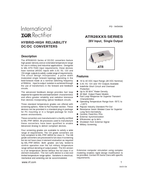
ATR2803R3S
Table I. Electrical performance Characteristics
Test Symbol Conditions -55°C ≤ TC ≤ +125°C VIN = 28VDC ±5%, CL = 0 Unless otherwise specified IOUT = 0 VIN = 16, 28, and 40 VDC VIN = 16, 28, and 40 VDC B.W. = 20Hz to 2 MHz VIN = 16, 28, and 40 VDC IOUT = 0, 3000, and 6000mA VIN = 16,28, and 40 VDC IOUT = 0, 3000, and 6000mA IOUT = 0, inhibit (pin 2) Tied to input return (pin 10) IOUT = 0, inhibit (pin 2) = open IOUT =6000mA B.W. = 20Hz to 2 MHz IOUT =6000mA Input to output or any pin to case (except pin 8) at 500 VDC, TC =+25°C No effect on dc performance TC =+25°C 6 Overload, TC = +25°C Short Circuit IOUT = 7500mA IOUT = 7500mA Load step 50% to/from 100% Load step 50% to/from 100% Load step 50% to/from 100% Load step 50% to/from 100% VOTLINE Input step 16V to/from 40VDC, IOUT = 7500mA Group A Subgroups Device Types Limits Min 1 2,3 1,2,3 1,2,3 1 2,3 1,2,3 1,2,3 1,2,3 1 2,3 1 4 1 1,2,3 4,5,6 4,5,6 4,5,6 4,5,6 4 5,6 4 5,6 4,5,6 01 01 01 01 01 01 01 01 01 01 01 01 01 01 500 500 -500 -500 74 70 100 500 12 9 600 700 +500 +500 100 200 100 200 ±500 3.25 3.20 Max 3.35 3.40 7500 60 ±20 ±30 ±50 18 50 50 V mA mV p-p mV mV mA mA p-p % MΩ µF W KHz KHz mV pk Units
5962-8767904FC资料
Hermetically Sealed,Transistor Output OptocouplersReliability Data SheetDescriptionThe reliability data shown includes Agilent reliability test data from the past three years on this product family. All of these products use the same LEDs, the same logic gate ICs, the same DSCC approved packaging materials, processes, stress conditions and testing.The data in Tables 1 and 2 reflect actual test data on dual channel devices. The single channel HCPL-5501 data in Table 3 is inferred from the demonstrated life test data using the factor (1.5) found in the “Photodiode Detector Isolator” section of MIL-HDBK-217, combined with any single channel data obtained. This dataDefinition of FailureInability to switch, i.e., “functional failure”, is the definition of failure in this data sheet. Specifically,failure occurs when the device fails to switch ON with 2 times the minimum recommended drive current (but not exceeding the max. rating) or fails to switch OFF when there is no input current.Failure Rate ProjectionsThe demonstrated point mean time to failure (MTTF) is measured at the absolutemaximum stress condition. The failure rate projections in Tables 2and 3 use the Arrheniusacceleration relationship, where a 0.43 eV activation energy is used as in the hybrid section of MIL-HDBK-217.Applications InformationThe data of Tables 1, 2, and 3 were obtained on MIL-PRF-38534screened devices with high temperature operating life duration up to 5000 hours. An exponential (random) failuredistribution is assumed, expressed in units of FIT (failures per billionis taken from testing on Agilent Technologies devices using internal Agilent processes,material specifications, design standards, and statistical process controls. THEY ARE NOT TRANSFERABLE TO OTHER MANUFACTURERS’ SIMILAR PART TYPES.device hours) are only defined in the random failure portion of the reliability curve.For valid system reliability calculations, it is necessary to adjust for the time when the system is not in operation.Note that if you are using MIL-HDBK-217 for predictingcomponent reliability, the results may not be comparable to those given in Tables 2 and 3 due to the different conditions and factorsOperating Life TestTable 1. Demonstrated Operating Life Test Performance, 4N55/883BDemonstrated Demonstrated Stress Test Total Devices Total Device Number of MTTF (hr)@FITs @Condition Tested Hours Failed Units T A = +125°C T A = +125°C I f = 20 mA 4301,700,000>1,700,000<588I out = 25 mA V CC = 18 V T A = +125°C T j = +135°CAgilent5962-8767901EX, 5962-8767905KEX 4N55/883B, HCPL-257K5962-8767902PX, 5962-8767906KPX HCPL-5531, HCPL-553K5962-9085401HPX, 5962-9085401KPX HCPL-5501, HCPL-550K5962-87679032A, 5962-8767907K2A HCPL-6531, HCPL-653K5962-8767904FC, 5962-8767908KFC HCPL-6551, HCPL-655K Data subject to change.Copyright © 2000 Agilent Technologies, Inc.Obsoletes 5967-6010E 5968-9394E (2/00)Environmental TestingAll high reliability hermeticoptocouplers listed meet the 100%screening and qualityconformance inspection testing of MIL-PRF-38534, class H or class K as applicable.Table 4. ESDS Classification per Method 3015, MIL-STD-883that have been accounted for in MIL-HDBK-217. For example, it is unlikely that your application will exercise all available channels atfull rated power with the LED(s)always ON as Agilent testing does.Thus, your application total power and duty cycle must be carefullyconsidered when comparing Tables 2 and 3 to predictions using MIL-HDBK-217.Electrostatic Discharge SensitivityPart NumberESD Class 5962-8767905KEX, HCPL-257K 15962-8767901EX, 4N55/883B 15962-8767906KPX, HCPL-553K 35962-8767902PX, HCPL-553135962-9085401KPX, HCPL-550K 15962-9085401HPX, HCPL-550115962-8767907K2A, HCPL-653K 15962-87679032A, HCPL-653115962-8767908KFC, HCPL-655K 35962-8767904FC, HCPL-65513Table 3. Reliability Projections for Single Channel Devices Listed in Title Typical (60% Confidence)90% Confidence AmbientJunctionMTTF FITs MTTF FITs Temperature (°C)Temperature (°C)(hr/fail)(fail/109hr)(hr/fail)(fail/109hr))1251302,786,0003591,881,0005311201253,252,0003072,198,0004551101154,484,0002233,037,0003291001056,289,0001594,268,00023490958,983,0001116,110,000164808513,090,000768,924,000112707519,491,0005113,320,00075606529,713,0003420,359,00049505546,477,0002231,933,00031404574,774,0001351,525,000193035124,069,000885,760,000122530161,833,0006112,046,0009Table 2. Reliability Projections for Dual Channel Devices Listed in Title Typical (60% Confidence)90% Confidence AmbientJunctionMTTF FITs MTTF FITs Temperature (°C)Temperature (°C)(hr/fail)(fail/109hr)(hr/fail)(fail/109hr))1251351,855,000539738,0001,3541201302,159,000463859,0001,1641101202,959,0003381,177,0008491001104,122,0002431,640,000610901005,845,0001712,326,00043080908,450,0001183,362,000297708012,474,000804,964,000201607018,837,000537,496,000133506029,157,0003411,603,00086405046,370,0002218,452,00054304075,964,0001330,229,00033253598,403,0001039,158,00026。
5962-0625602QXC资料
Applications
• Video amplifiers • Cable drivers • RGB amplifiers • Test equipment • Instrumentation • Current to voltage converters
Ordering Information
Pinouts
5962-0625601QXC (10 LD FLAT PACK) TOP VIEW
1 2 3 4 5 NC ININ+ VSNC NC NC CE VS+ OUT 10 9 8 7 6 1 2 3 4 5
5962-0625602QXC (10 LD FLAT PACK) TOP VIEW
DESCRIPTION
AV = +1 AV = +2
1400 800 100 6000 8 1.7 19 50
MHz MHz MHz V/µs ns nV/√Hz pA/√Hz pA/√Hz % °
BW1 SR tS eN iNiN+ dG dP
0.1dB Bandwidth Slew Rate 0.1% Settling Time Input Voltage Noise IN- Input Current Noise IN+ Input Current Noise Differential Gain Error (Note 3) Differential Phase Error (Note 3)
元器件交易网
5962-0625601QXC, 5962-0625602QXC
Absolute Maximum Ratings (TA = +25°C)
Supply Voltage between VS+ and VS- . . . . . . . . . . . . . . . . . . . 12.6V Slewrate between VS+ and VS- . . . . . . . . . . . . . . . . . . . . . . . . 1V/µs Maximum Continuous Output Current . . . . . . . . . . . . . . . . . . . 20mA I into VIN+, VIN-, Enable Pins . . . . . . . . . . . . . . . . . . . . . . . . . ±4mA Pin Voltages . . . . . . . . . . . . . . . . . . . . . . . . . VS- -0.5V to VS+ +0.5V
- 1、下载文档前请自行甄别文档内容的完整性,平台不提供额外的编辑、内容补充、找答案等附加服务。
- 2、"仅部分预览"的文档,不可在线预览部分如存在完整性等问题,可反馈申请退款(可完整预览的文档不适用该条件!)。
- 3、如文档侵犯您的权益,请联系客服反馈,我们会尽快为您处理(人工客服工作时间:9:00-18:30)。
1/11May 2004s LOW DROPOUT VOLTAGEsEMBEDDED OVERTEMPERATURE,OVERCURRENT PROTECTIONSs ADJUSTABLE CURRENT LIMITATION sOUTPUT OVERLOAD MONITORING/SIGNALLINGs FIXED 2.5;3.3V;5.0V OUTPUT VOLTAGES sINHIBIT (ON/OFF)TTL COMPATIBLE CONTROLsPROGRAMMABLE OUTPUT SHORT CIRCUIT CURRENTs REMOTE SENSING OPERATIONsRADHARD:TESTED UP TO 300krad IN MIL 1019.5AND LOW DOSE RATE CONDITIONS sHEAVY IONS SEL,SEU FREE.SUSTAINS 2x10¹⁴proton/cm 2,AND 2x10¹⁴neutron/cm²DESCRIPTIONThe RHFL4913Fixed is a high performance Rad Hard Positive Voltage Regulator family.Available into various hermetic ceramic packages,it is specifically intended for Space and harshradiation environments.Input supply range is from 3to 12volts.RHFL4913Fixed is Qml-V Qualified,DSCC Smd are 5962F02534/02535/02536/02537.RHFL4913FIXED VERSIONRAD-HARD POSITIVE FIXEDVOLTAGEREGULATORSRHFL4913FIXED VERSION2/11Table 1:Absolute Maximum Ratings (Note 1)Note 1:Exceeding maximum ratings may damage the device.Table 2:Thermal DataFigure 1:Connection Diagram (Top view,Bottom view for SMD.5)Table 3:Pin DescriptionSymbol ParameterValue Unit V I DC Input Voltage,V I -V GROUND 14V I O Output CurrentRHFL4913S,ESY 3A RHFL4913KP2P D T C =25°C Power Dissipation 15W T stg Storage Temperature Range-65to +150°C T op Operating Junction Temperature Range -55to +150°CESDElectrostatic Discharge CapabilityClass 3Symbol ParameterFPC-16TO-257SMD.5Unit R thj-case Thermal Resistance Junction-case 8.38.38.3°C/W T soldMaximum soldering Temperature,10sec.300°CPIN N°FPC-16SMD.5TO-257V O 1,2,6,713V I 3,4,521GND 1332I SC 8OCM 10INHIBIT 14SENSE 16NC9,11,12,15RHFL4913FIXED VERSION3/11Table 4:Ordering CodesTable 5:Part Number -Smd EquivalenceNote:3V version is available on request.Table 6:Environmental CharacteristicsFPC-16SMD.5TO-257SOLDER DIPPINGOUTPUT VOLTAGE RHFL4913KP25-01V RHFL4913S25-03V RHFL4913ESY2505V GOLD 2.5V RHFL4913KP25-02V RHFL4913S25-04V RHFL4913ESY2506V SOLDER 2.5V RHFL4913KP30-01V RHFL4913S30-03V RHFL4913ESY3005V GOLD 3.0V RHFL4913KP30-02V RHFL4913S30-04V RHFL4913ESY3006V SOLDER 3.0V RHFL4913KP33-01V RHFL4913S33-03V RHFL4913ESY3305V GOLD 3.3V RHFL4913KP33-02V RHFL4913S33-04V RHFL4913ESY3306V SOLDER 3.3V RHFL4913KP50-01V RHFL4913S50-03V RHFL4913ESY5005V GOLD 5.0V RHFL4913KP50-02VRHFL4913S50-04VRHFL4913ESY5006VSOLDER5.0VST PART NUMBER SMD PART NUMBER RHFL4913KP25-01V 5962F0253401VXC RHFL4913KP25-02V 5962F0253401VXA RHFL4913KP33-01V 5962F0253501VXC RHFL4913KP33-02V 5962F0253501VXA RHFL4913KP50-01V 5962F0253601VXC RHFL4913KP50-02V 5962F0253601VXA RHFL4913S25-03V 5962F0253402VYC RHFL4913S25-04V 5962F0253402VYA RHFL4913S33-03V 5962F0253502VYC RHFL4913S33-04V 5962F0253502VYA RHFL4913S50-03V 5962F0253602VYC RHFL4913S50-04V 5962F0253602VYA RHFL4913ESY2505V 5962F0253402VZC RHFL4913ESY2506V 5962F0253402VZA RHFL4913ESY3305V 5962F0253502VZC RHFL4913ESY3306V 5962F0253502VZA RHFL4913ESY5005V 5962F0253602VZC RHFL4913ESY5006V5962F0253602VZAParameterConditionsTypical Unit Output Voltage thermal drift -55°C to 125°C40ppm/°C Output Voltage radiation drift from 0krad to 300krad at 0.55rad/sec 8ppm/krad Output Voltage radiation driftfrom 0krad to 300krad,Mil 1019.56ppm/kradRHFL4913FIXED VERSION4/11Table 7:Electrical Characteristics (T J =25°C,V I =V O +2.5V,C I =C O =1µF,unless otherwise speci-fied)(*)This value is guaranteed by design.For each application it’s strongly recommended to comply with the maximum current limit of the pack-age used.Symbol ParameterTest ConditionsMin.Typ.Max.Unit V I Operating Input Voltage I O =1AT J =-55to 125°C312V V O Output Voltage accuracy V I =V O +2.5V,I O =5mA-22%I SHORT Output Current Limit (*)Adjustable by mask/external resistor4.5A V O Operating Output Voltage I O =2A,2.5V output voltage 2.45 2.55V V O Operating Output Voltage I O =2A,3.3V output voltage 3.23 3.37V V OOperating Output Voltage I O =2A,5.0V output voltage4.95.1V ∆V O /∆V I Line Regulation V I =V O +2.5V to 12V,I O =5mA 0.35%∆V O /∆V O Load Regulation V I =V O +2.5V,I O =5mA to 400mA 0.3%V I =V O +2.5V,I O =5mA to 1A 0.5%Z OUT Output Impedance I O =100mA DC and 20mA rms 100m ΩI qQuiescent CurrentV I =V O +2.5V,I O =5mA On Mode 6mAV I =V O +2.5V,I O =30mA On Mode 8V I =V O +2.5V,I O =300mA On Mode 25V I =V O +2.5V,I O =1A On Mode 60V I =V O +2V,V INH =2.4VOff Mode1I qQuiescent CurrentV I =V O +2.5V,I O =5mA,T J =-55to 125°C 6mAV I =V O +2.5V,I O =30mA,T J =-55to 125°C 14V I =V O +2.5V,I O =300mA,T J =-55to 125°C 40V I =V O +2.5V,I O =1A,T J =-55to 125°C100V dDropout Voltage I O =400mAV O =2.5to 9V,(-55°C)300400V Dropout VoltageI O =400mAV O =2.5to 9V,(25°C)350450I O =1A V O =2.5to 9V,(25°C)650I O =2AV O =2.5to 9V,(25°C)900Dropout VoltageI O =400mAV O =2.5to 9V,(125°C)450550I O =1A V O =2.5to 9V,(125°C)800I O =2AV O =2.5to 9V,(125°C)950V INH(ON)Inhibit Voltage I O =5mA,T J =-55to 125°C 0.8V V INH(OFF)Inhibit Voltage I O =5mA,T J =-55to 125°C 2.4V SVR Supply Voltage Rejection V I =V O +2.5V ±0.5V,I O =5mA f =120Hz 6070dB f =33KHz3040I SH Shutdown Input Current V INH =5V15µA V OCM OCM Pin Voltage Sinked I OCM =10mA active low0.38V t PLH t PHL Inhibit Propagation Delay V I =V O +2.5V,V INH =2.4V,I O =400mA ON-OFF 20µS OFF-ON100µS eNOutput Noise VoltageB=10Hz to 100KHzI O =5mA to 2A40µVrmsRHFL4913FIXED VERSION5/11Figure 2:Application Diagram For Remote Sensins OperationDEVICE DESCRIPTIONThe RHFL4913Fixed Voltage contains a PNP type power element controlled by a signal resulting from amplified comparison between the internal temperature compensated Band-Gap cell and the fraction of the desired Output Voltage value.This fractional value is obtained from an internal-to-die resistor divider bridge set by STMicroelectronics.The device is protected by several functional blocks.Low pin count Package limitationsSome functions (INHIBIT,OCM,SENSE)are not available due to lack of pins.Corresponding die pads are by default connected inside silicon.SENSE pinThe Load voltage is applied by a Kelvin line connected to SENSE pin:Voltage feed-back comes from the internal divider resistor bridge.Therefore possible output voltages are set by manufacturer mask metal options.SENSE pin is not available in 3pin packages.INHIBIT ON-OFF ControlBy setting INHIBIT pin TTL-High,the Device switches off the Output Current and Voltage.The Device is ON when INHIBIT pin is set Low.Since INHIBIT pin is internally pulled down,it can be left floating in case Inhibit function is not utilized.INHIBIT pin is not available in 3pin packages.Overtemperature protectionA temperature detector internally monitors the power element junction temperature.The Device goes OFF at approx.175°C,returning to ON mode when back to approx.40°C.It is worth noting that when the internal temperature detector reaches 175°C,the active power element can be at 225°C:Device reliability cannot be granted in case of extensive operation under these conditions.Overcurrent protectionI SC pin.An internal non-fold back Short-Circuit limitation is set with I SHORT >3.8A (V O is 0V).This value can be reduced by an external resistor connected between I SC pin and V I pin,with a typical value range of 10k Ωto 200k Ω.This adjustment feature is not available in 3pin packages.To keep excellent V O regulation,it is necessary to set I SHORT 1.6times greater than the maximum desired application I O .When I O reaches I SHORT –300mA,the current limiter overrules Regulation and V O starts to drop and the OCM flag is risen.When no current limitation adjustment is required,I SC pin must be left unbiased (as it is in 3pin packages).OCM pinGoes Low when current limiter starts to be active,otherwise V OCM =V I .It is bufferized and can sink 10mA.OCM pin is internally pulled-up by a 5k Ωresistor.Not available in 3pinpackages.RHFL4913FIXED VERSIONAlternate toRHFL4913Fixed(&custom)Voltages replace all3-terminal Industry Devices,providing essential benefits -Lower Drop-Out-High radiation performance-Better SVR-Saving the high stability external setting resistors.APPLICATION INFORMATIONThe RHFL4913Fixed Voltage is functional as soon as V I-V O voltage difference is slightly above the power element saturation voltage.A minimum0.5mA I O ensures perfect“no-load”regulation.All available V I pins must always be externally interconnected,same thing for all available V O pins, otherwise Device stability and reliability cannot be granted.All NC pins can be connected to Ground.The INHIBIT function switches off the output current in an electronic way,that is very quickly.According to Lenz’s Law,external circuitry reacts with–LdI/dt terms which can be of high amplitude in case some series-inductance exists.The effect would be a large transient voltage developed on both Device terminals.It is necessary to protect the Device with Schottky diodes preventing negative voltage excursions.In the worst case,a14V Zener diode shall protect the Device Input.The Device has been designed for high stability and low drop out operation:Minimum1µF input and output tantalum capacitors are therefore mandatory.Capacitor ESR range is from0.5Ωto over20Ω. Such range turns out to be useful when ESR increases at low temperature.When large transient currents are expected,larger value capacitors are necessary.In case of high current operation with expected short-circuit events,caution must be considered relatively to capacitors.They must be connected as close as possible to device terminals.As some tantalum capacitors may permanently fail when submitted to high charge-up surge currents,it is recommended to decouple them with470nF polyester capacitors.Being RHFL4913Fixed Voltage manufactured with very high speed bipolar technology6GHz f T transistors),the PCB lay-out must be performed with extreme care,very low inductance,low mutually coupling lines,otherwise high frequency parasitic signals may be picked-up by the Device resulting into er’s benefit is a SVR performance extended to far higher frequencies.REMOTE SENSING OPERATIONIn case the Load is located far from the regulator,it is recommended to comply with the scheme below.To obtain the best regulation,it is in addition essential to care about:-The wire connecting R2to the Load end must not be crossed by the Load current(Kelvin sense).The noise captured by the wires between the Load and the chip could bring a noisy output voltage.In case this happens,it is recommended that shielded cables are used for these connections.The external wrap must be used for connecting the ground of the chip with the Load Ground.It is also recommended to place 1uF tantalum capacitors between Output and Ground close to the device and another next to the Load. 6/11RHFL4913FIXED VERSION7/11DIM.mm.inchMIN.TYPMAX.MIN.TYP.MAX.A 2.162.720.0850.107b 0.430.017c 0.130.005D 9.910.390E 6.910.272E2 4.320.170E30.760.030e 1.270.050L 6.720.265Q 0.66 1.140.0260.045S10.130.005ALN FPC-16 (MIL-STD-1835) MECHANICAL DATA7450901A1816eb cLE DS1QAE2E3LE39RHFL4913FIXED VERSION8/11DIM.mm.inchMIN.TYPMAX.MIN.TYP.MAX.A 3.000.118A10.380.015b7.260.286b1 5.720.225b2 2.410.095b3 3.050.120D10.160.400D10.760.030E7.520.296e 1.910.075SMD.5 MECHANICAL DATA7386434ARHFL4913FIXED VERSION9/11DIM.mm.inch MIN.TYP MAX.MIN.TYP.MAX.A 10.540.415B 10.540.415C 16.640.655D 4.75.330.1850.210E 1.020.40F 3.56 3.68 3.810.1400.1450.150G 13.510.532H 5.260.207I 0.760.030J 3.050.120K 2.540.100L 15.216.50.5980.650M 2.290.090N 0.710.028R1.650.065TO-257 MECHANICAL DATA0117268CRHFL4913FIXED VERSIONTable8:Revision HistoryDate Revision Description of Changes 05-May-20045Mistake in Pin description SMD.5on Table310/11RHFL4913FIXED VERSION Information furnished is believed to be accurate and reliable. However, STMicroelectronics assumes no responsibility for the consequences of use of such information nor for any infringement of patents or other rights of third parties which may result from its use. No license is granted by implication or otherwise under any patent or patent rights of STMicroelectronics. Specifications mentioned in this publication are subject to change without notice. This publication supersedes and replaces all information previously supplied. STMicroelectronics products are not authorized for use as critical components in life support devices or systems without express written approval of STMicroelectronics.The ST logo is a registered trademark of STMicroelectronicsAll other names are the property of their respective owners© 2004 STMicroelectronics - All Rights ReservedSTMicroelectronics GROUP OF COMPANIESAustralia - Belgium - Brazil - Canada - China - Czech Republic - Finland - France - Germany - Hong Kong - India - Israel - Italy - Japan - Malaysia - Malta - Morocco - Singapore - Spain - Sweden - Switzerland - United Kingdom - United States.11/11。