MT41J64M16JT-15E IT_G
MEMORY存储芯片MT41J64M16JT-125G中文规格书
Active Power-Down Current (AL = 0) CKE: LOW; External clock: on; tCK, CL: see the previous table; BL: 8;1 AL: 0; CS_n: stable at 1; Command, address, bank group address, bank address inputs: stable at 1; Data I/O: VDDQ; DM_n: stable at 1; Bank activity: all banks open; Output buffer and RTT: Enabled in mode registers;2 ODT signal: stable at 0
Precharge Standby ODT Current CKE: HIGH; External clock: on; tCK, CL: see the previous table; BL: 8;1 AL: 0; CS_n: stable at 1; Command, address, bank gropup address, bank address inputs: partially toggling according to the IDD2NT Measurement-Loop Pattern table; Data I/O: VSSQ; DM_n: stable at 1; Bank activity: all banks closed; Output buffer and RTT: enabled in mode registers;2 ODT signal: toggling according to the IDD2NT Measurement-Loop Pattern table; Pattern details: see the IDD2NT Measurement-Loop Pattern table
MEMORY存储芯片MT41J64M16JT-093G G中文规格书
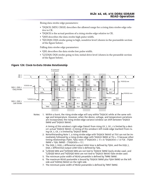
Rising data strobe edge parameters:•t DQSCK (MIN)/(MAX) describes the allowed range for a rising data strobe edge rela-tive to CK.•t DQSCK is the actual position of a rising strobe edge relative to CK.•t QSH describes the data strobe high pulse width.•t HZ(DQS) DQS strobe going to high, nondrive level (shown in the postamble section of the figure below).Falling data strobe edge parameters:•t QSL describes the data strobe low pulse width.•t LZ(DQS) DQS strobe going to low, initial drive level (shown in the preamble section of the figure below).Figure 126: Clock-to-Data Strobe RelationshipRL measuredDQS_t, DQS_cEarly StrobeCK_tCK_cDQS_t, DQS_cLate StrobeNotes: 1.Within a burst, the rising strobe edge will vary within t DQSCKi while at the same volt-age and temperature. However, when the device, voltage, and temperature variations are incorporated, the rising strobe edge variance window can shift between t DQSCK (MIN) and t DQSCK (MAX).A timing of this window's right edge (latest) from rising CK_t, CK_c is limited by a devi-ce's actual t DQSCK (MAX). A timing of this window's left inside edge (earliest) from ris-ing CK_t, CK_c is limited by t DQSCK (MIN).2.Notwithstanding Note 1, a rising strobe edge with t DQSCK (MAX) at T(n) can not be im-mediately followed by a rising strobe edge with t DQSCK (MIN) at T(n + 1) because other timing relationships (t QSH, t QSL) exist: if t DQSCK(n + 1) < 0: t DQSCK(n) < 1.0 t CK - (t QSH (MIN) + t QSL (MIN)) - | t DQSCK(n + 1) |.3.The DQS_t, DQS_c differential output HIGH time is defined by t QSH, and the DQS_t,DQS_c differential output LOW time is defined by t QSL.4.t LZ(DQS) MIN and t HZ(DQS) MIN are not tied to t DQSCK (MIN) (early strobe case), and t LZ(DQS) MAX and t HZ(DQS) MAX are not tied to t DQSCK (MAX) (late strobe case).5.The minimum pulse width of READ preamble is defined by t RPRE (MIN).6.The maximum READ postamble is bound by t DQSCK (MIN) plus t QSH (MIN) on the left side and t HZDSQ (MAX) on the right side.7.The minimum pulse width of READ postamble is defined by t RPST (MIN).8Gb: x4, x8, x16 DDR4 SDRAM READ OperationFigure 170: Rx Mask DQ-to-DQS Timings DQS, DQs Data-In at DRAM Ball DQS, DQs Data-In at DRAM BallRx Mask Rx Mask – Alternative ViewDRAMbDRAMb Notes: 1.DQx represents an optimally centered mask.DQy represents earliest valid mask.DQz represents latest valid mask.2.DRAMa represents a DRAM without any DQS/DQ skews.DRAMb represents a DRAM with early skews (negative t DQS2DQ).DRAMc represents a DRAM with delayed skews (positive t DQS2DQ).3.This figure shows the skew allowed between DRAM-to-DRAM and between DQ-to-DQ for a DRAM. Signals assume data is center-aligned at DRAM latch.TdiPW is not shown; composite data-eyes shown would violate TdiPW.V CENTDQ,midpoint is not shown but is assumed to be midpoint of V diVW .The previous figure shows the basic Rx mask requirements. Converting the Rx mask re-quirements to a classical DQ-to-DQS relationship is shown in the following figure. It should become apparent that DRAM write training is required to take full advantage of the Rx mask.8Gb: x4, x8, x16 DDR4 SDRAM WRITE Operation。
MEMORY存储芯片MT41K128M16JT-125 IT中文规格书
–V DD and V DDQ are driven from a single-power converter output and applyV DD /V DDQ without any slope reversal before or at the same time as V TT andV REFCA .–The voltage levels on all balls other than V DD , V DDQ , V SS , and V SSQ must be lessthan or equal to V DDQ and V DD on one side and must be greater than or equalto V SSQ and V SS on the other side.–V TT is limited to 0.76V MAX when the power ramp is complete.–V REFCA tracks V DD /2.•Condition B:–Apply V PP without any slope reversal before or at the same time as V DD .–Apply V DD without any slope reversal before or at the same time as V DDQ .–Apply V DDQ without any slope reversal before or at the same time as V TT andV REFCA .–The voltage levels on all pins other than V PP , V DD , V DDQ , V SS , and V SSQ must beless than or equal to V DDQ and V DD on one side and must be larger than orequal to V SSQ and V SS on the other side.2.After RESET_n is de-asserted, wait for a minimum of 500μs, but no longer than 3seconds, before allowing CKE to be registered HIGH at clock edge Td. During thistime, the device will start internal state initialization; this will be done independ-ently of external clocks. A reasonable attempt was made in the design to power upwith the following default MR settings: gear-down mode (MR3 A[3]): 0 = 1/2 rate;per-DRAM addressability (MR3 A[4]): 0 = disable; maximum power-down (MR4A[1]): 0 = disable; CS to command/address latency (MR4 A[8:6]): 000 = disable; CAparity latency mode (MR5 A[2:0]): 000 = disable. However, it should be assumedthat at power up the MR settings are undefined and should be programmed asshown below.3.Clocks (CK_t, CK_c) need to be started and stabilized for at least 10ns or 5 t CK(whichever is larger) before CKE is registered HIGH at clock edge Td. Because CKEis a synchronous signal, the corresponding setup time to clock (t IS) must be met.Also, a DESELECT command must be registered (with t IS setup time to clock) atclock edge Td. After the CKE is registered HIGH after RESET, CKE needs to be con-tinuously registered HIGH until the initialization sequence is finished, includingexpiration of t DLLK and t ZQinit.4.The device keeps its ODT in High-Z state as long as RESET_n is asserted. Further,the SDRAM keeps its ODT in High-Z state after RESET_n de-assertion until CKE isregistered HIGH. The ODT input signal may be in an undefined state until t IS be-fore CKE is registered HIGH. When CKE is registered HIGH, the ODT input signalmay be statically held either LOW or HIGH. If R TT(NOM) is to be enabled in MR1,the ODT input signal must be statically held LOW. In all cases, the ODT input sig-nal remains static until the power-up initialization sequence is finished, includingthe expiration of t DLLK and t ZQinit.5.After CKE is registered HIGH, wait a minimum of RESET CKE EXIT time, t XPR, be-fore issuing the first MRS command to load mode register (t XPR = MAX (t XS, 5 ×t CK).6.Issue MRS command to load MR3 with all application settings, wait t MRD.7.Issue MRS command to load MR6 with all application settings, wait t MRD.8.Issue MRS command to load MR5 with all application settings, wait t MRD.9.Issue MRS command to load MR4 with all application settings, wait t MRD.10.Issue MRS command to load MR2 with all application settings, wait t MRD.11.Issue MRS command to load MR1 with all application settings, wait t MRD.8Gb: x4, x8, x16 DDR4 SDRAM RESET and Initialization ProcedureFigure 38: MPR READ-to-WRITE TimingT0T1T2DQ DQS_t,DQS_cTa0Ta1Ta2Ta3Ta4Ta5Ta6Tb0Tb1Tb2Command Address CKECK_tCK_cDon’t CareNotes: 1.Address setting:A[1:0] = 00b (data burst order is fixed starting at nibble, always 00b here)A2 = 0b (for BL = 8, burst order is fixed at 0, 1, 2, 3, 4, 5, 6, 7)BA1 and BA0 indicate the MPR locationA10 and other address pins are "Don’t Care," including BG1 and BG0. A12 is "Don’tCare" when MR0 A[1:0] = 00 and must be 1b when MR0 A[1:0] = 012.Address setting:BA1 and BA0 indicate the MPR locationA[7:0] = data for MPRBA1 and BA0 indicate the MPR locationA10 and other address pins are "Don’t Care"3.Parity latency (PL) is added to data output delay when CA parity latency mode is ena-bled.MPR WritesMPR access mode allows 8-bit writes to the MPR Page 0 using the address bus A[7:0].Data bus inversion (DBI) is not allowed during MPR WRITE operation. The DRAM willmaintain the new written values unless re-initialized or there is power loss.The following steps are required to use the MPR to write to mode register MPR Page 0.1.The DLL must be locked if enabled.2.Precharge all; wait until t RP is satisfied.3.MRS command to MR3[2] = 1 (enable MPR data flow) and MR3[1:0] = 00 (MPRPage 0); writes to 01, 10, and 11 are not allowed.4.t MRD and t MOD must be satisfied.5.Redirect all subsequent WRITE commands to specific MPR x location.6.Issue WR or WRA command:a.BA1 and BA0 indicate MPR x location1.00 = MPR02.01 = MPR13.10 = MPR24.11 = MPR3b.A[7:0] = data for MPR Page 0, mapped A[7:0] to UI[7:0].8Gb: x4, x8, x16 DDR4 SDRAM Multipurpose Register。
MEMORY存储芯片MT41J256M16RE-15EIT中文规格书

10.Release frame sync generators from reset.Note that it is necessary to release the internal frame syncgenerators from reset,even if an external frame sync is being used,because the frame sync errordetection logic is built into the frame sync generator.(a)Take the respective frame sync generator(s)out of reset by setting the RFRST bit for the receiver,and/or the XFRST bit for the transmitter in GBLCTL.All other bits in GBLCTL should be left at theprevious state.(b)Read back from GBLCTL to ensure the bit(s)to which you wrote are successfully latched inGBLCTL before you proceed.11.Upon the first frame sync signal,McASP transfers begin.The McASP synchronizes to an edge on theframe sync pin,not the level on the frame sync pin.This makes it easy to release the state machineand frame sync generators from reset.(a)For example,if you configure the McASP for a rising edge transmit frame sync,then you do notneed to wait for a low level on the frame sync pin before releasing the McASP transmitter statemachine and frame sync generators from reset.23.0.21.1.3Separate Transmit and Receive InitializationIn many cases,it is desirable to separately initialize the McASP transmitter and receiver.For example,you may delay the initialization of the transmitter until the type of data coming in on the receiver is recognized.Or a change in the incoming data stream on the receiver may necessitate a reinitialization of thetransmitter.In this case,you may still follow the sequence outlined in Section23.0.21.1.2,but use it for each section (transmit,receive)individually.The GBLCTL register is aliased to RGBLCTL and XGBLCTL to facilitate separate initialization of transmit and receive sections.Also,make sure that the initialization or reinitialization sequence follows the guidelines in Bits WithRestrictions on When They May be Changed.23.0.21.1.4Importance of Reading Back GBLCTLIn Section23.0.21.1.2,steps4b,5b,7c,9b,and10b state that GBLCTL should be read back until the bits that were written are successfully latched.This is important,because the transmitter and receiver state machines run off of the respective bit clocks,which are typically about tens to hundreds of times slower than the DSP's internal bus clock.Therefore,it takes many cycles between when the DSP writes toGBLCTL(or RGBLCTL and XGBLCTL),and when the McASP actually recognizes the write operation.If you skip this step,then the McASP may never see the reset bits in the global control registers getasserted and deasserted;resulting in an uninitialized McASP.Therefore,the logic in McASP has been implemented such that once the DSP writes GBLCTL,RGBLCTL, or XGBLCTL,the resulting write is not visible by reading back GBLCTL until the McASP has recognized the change.This typically requires two bit clocks plus two DSP bus clocks to occur.Also,if the bit clocks can be completely stopped,any software that polls GBLCTL should be implemented with a time-out.If GBLCTL does not have a time-out,and the bit clock stops,the changes written toGBLCTL will not be reflected until the bit clock restarts.Finally,please note that while RGBLCTL and XGBLCTL allow separate changing of the receive andtransmit halves of GBLCTL,they also immediately reflect the updated value(useful for debug purposes).Only GBLCTL can be used for the read back step.23.0.21.1.5Synchronous Transmit and Receive Operation(ASYNC=0)When ASYNC=0in ACLKXCTL,the transmit and receive sections operate synchronously from thetransmit section clock and transmit frame sync signals(Figure23-15).The receive section may have a different(but compatible in terms of slot size)data format.Note that when ASYNC=0,XCLK isautomatically inverted to produce RCLK(note the inversion on the ASYNC multiplexer as shown inFigure23-16).Table23-3.Channel Status and User Data for Each DIT BlockFrame Subframe Preamble Channel Status defined in:User Data defined in: Defined by DITCSRA0,DITCSRB0,DITUDRA0,DITUDRB001(L)B DITCSRA0[0]DITUDRA0[0]02(R)W DITCSRB0[0]DITUDRB0[0]11(L)M DITCSRA0[1]DITUDRA0[1]12(R)W DITCSRB0[1]DITUDRB0[1]21(L)M DITCSRA0[2]DITUDRA0[2]22(R)W DITCSRB0[2]DITUDRB0[2]……………311(L)M DITCSRA0[31]DITUDRA0[31]312(R)W DITCSRB0[31]DITUDRB0[31] Defined by DITCSRA1,DITCSRB1,DITUDRA1,DITUDRB1321(L)M DITCSRA1[0]DITUDRA1[0]322(R)W DITCSRB1[0]DITUDRB1[0]……………631(L)M DITCSRA1[31]DITUDRA1[31]632(R)W DITCSRB1[31]DITUDRB1[31] Defined by DITCSRA2,DITCSRB2,DITUDRA2,DITUDRB2641(L)M DITCSRA2[0]DITUDRA2[0]642(R)W DITCSRB2[0]DITUDRB2[0]……………951(L)M DITCSRA2[31]DITUDRA2[31]952(R)W DITCSRB2[31]DITUDRB2[31] Defined by DITCSRA3,DITCSRB3,DITUDRA3,DITUDRB3961(L)M DITCSRA3[0]DITUDRA3[0]962(R)W DITCSRB3[0]DITUDRB3[0]……………1271(L)M DITCSRA3[31]DITUDRA3[31]1272(R)W DITCSRB3[31]DITUDRB3[31] Defined by DITCSRA4,DITCSRB4,DITUDRA4,DITUDRB41281(L)M DITCSRA4[0]DITUDRA4[0]1282(R)W DITCSRB4[0]DITUDRB4[0]……………1591(L)M DITCSRA4[31]DITUDRA4[31]1592(R)W DITCSRB4[31]DITUDRB4[31] Defined by DITCSRA5,DITCSRB5,DITDRA5,DITUDRB51601(L)M DITCSRA5[0]DITUDRA5[0]1602(R)W DITCSRB5[0]DITUDRB5[0]……………1911(L)M DITCSRA5[31]DITUDRA5[31]1912(R)W DITCSRB5[31]DITUDRB5[31]。
MEMORY存储芯片MT41J128M16HA-15EIT中文规格书
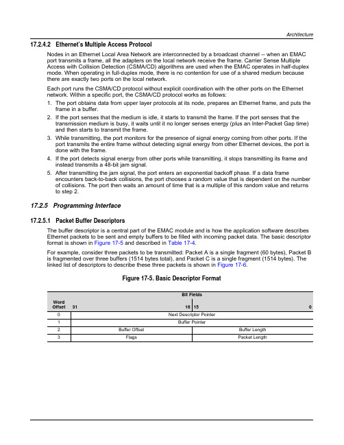
Architecture 17.2.4.2Ethernet’s Multiple Access ProtocolNodes in an Ethernet Local Area Network are interconnected by a broadcast channel--when an EMAC port transmits a frame,all the adapters on the local network receive the frame.Carrier Sense MultipleAccess with Collision Detection(CSMA/CD)algorithms are used when the EMAC operates in half-duplex mode.When operating in full-duplex mode,there is no contention for use of a shared medium because there are exactly two ports on the local network.Each port runs the CSMA/CD protocol without explicit coordination with the other ports on the Ethernet network.Within a specific port,the CSMA/CD protocol works as follows:1.The port obtains data from upper layer protocols at its node,prepares an Ethernet frame,and puts theframe in a buffer.2.If the port senses that the medium is idle,it starts to transmit the frame.If the port senses that thetransmission medium is busy,it waits until it no longer senses energy(plus an Inter-Packet Gap time)and then starts to transmit the frame.3.While transmitting,the port monitors for the presence of signal energy coming from other ports.If theport transmits the entire frame without detecting signal energy from other Ethernet devices,the port isdone with the frame.4.If the port detects signal energy from other ports while transmitting,it stops transmitting its frame andinstead transmits a48-bit jam signal.5.After transmitting the jam signal,the port enters an exponential backoff phase.If a data frameencounters back-to-back collisions,the port chooses a random value that is dependent on the number of collisions.The port then waits an amount of time that is a multiple of this random value and returnsto step2.17.2.5Programming Interface17.2.5.1Packet Buffer DescriptorsThe buffer descriptor is a central part of the EMAC module and is how the application software describes Ethernet packets to be sent and empty buffers to be filled with incoming packet data.The basic descriptor format is shown in Figure17-5and described in Table17-4.For example,consider three packets to be transmitted:Packet A is a single fragment(60bytes),Packet B is fragmented over three buffers(1514bytes total),and Packet C is a single fragment(1514bytes).The linked list of descriptors to describe these three packets is shown in Figure17-6.Figure17-5.Basic Descriptor FormatBit FieldsWordOffset3116150 0Next Descriptor Pointer1Buffer Pointer2Buffer Offset Buffer Length3Flags Packet LengthIntroduction 17.1Introduction17.1.1Purpose of the PeripheralThe EMAC module is used to move data between the device and another host connected to the same network,in compliance with the Ethernet protocol.The EMAC controls the flow of packet data from the system to the PHY.The MDIO module controls PHY configuration and status monitoring.Both the EMAC and the MDIO modules interface to the system core through a custom interface thatallows efficient data transmission and reception.This custom interface is referred to as the EMAC control module and is considered integral to the EMAC/MDIO peripheral.17.1.2FeaturesThe EMAC/MDIO has the following features:•Synchronous10/100Mbps operation.•Standard Media Independent Interface(MII)and/or Reduced Media Independent Interface(RMII)to physical layer device(PHY).•EMAC acts as DMA master to either internal or external device memory space.•Eight receive channels with VLAN tag discrimination for receive quality-of-service(QOS)support.•Eight transmit channels with round-robin or fixed priority for transmit quality-of-service(QOS)support.•Ether-Stats and802.3-Stats statistics gathering.•Transmit CRC generation selectable on a per channel basis.•Broadcast frames selection for reception on a single channel.•Multicast frames selection for reception on a single channel.•Promiscuous receive mode frames selection for reception on a single channel(all frames,all good frames,short frames,error frames).•Hardware flow control.•8k-byte local EMAC descriptor memory that allows the peripheral to operate on descriptors without affecting the CPU.The descriptor memory holds enough information to transfer up to512Ethernetpackets without CPU intervention.(This memory is also known as CPPI RAM.)•Programmable interrupt logic permits the software driver to restrict the generation of back-to-back interrupts,which allows more work to be performed in a single call to the interrupt service routine.。
MEMORY存储芯片MT41K128M16JT-125 M AIT K中文规格书
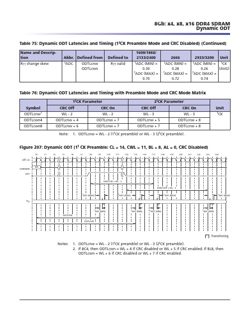
Table 75: Dynamic ODT Latencies and Timing (1t CK Preamble Mode and CRC Disabled) (Continued)Table 76: Dynamic ODT Latencies and Timing with Preamble Mode and CRC Mode MatrixNote: 1.ODTLcnw = WL - 2 (1t CK preamble) or WL - 3 (2t CK preamble).Figure 207: Dynamic ODT (1t CK Preamble; CL = 14, CWL = 11, BL = 8, AL = 0, CRC Disabled)diff_CKCommandODTR TT TransitioningNotes: 1.ODTLcnw = WL - 2 (1t CK preamble) or WL - 3 (2t CK preamble).2.If BC4, then ODTLcwn = WL + 4 if CRC disabled or WL + 5 if CRC enabled; If BL8, thenODTLcwn = WL + 6 if CRC disabled or WL + 7 if CRC enabled.8Gb: x4, x8, x16 DDR4 SDRAM Dynamic ODT7.Early data transitions may not always happen at the same DQ. Data transitions of a DQ can vary (either early or late) within a burst.t LZ(DQS), t LZ(DQ), t HZ(DQS), and t HZ(DQ) Calculationst HZ and t LZ transitions occur in the same time window as valid data transitions. These parameters are referenced to a specific voltage level that specifies when the device out-put is no longer driving t HZ(DQS) and t HZ(DQ), or begins driving t LZ(DQS) and t LZ(DQ). The figure below shows a method to calculate the point when the device is no longer driving t HZ(DQS) and t HZ(DQ), or begins driving t LZ(DQS) and t LZ(DQ), by measuring the signal at two different voltages. The actual voltage measurement points are not critical as long as the calculation is consistent. t LZ(DQS), t LZ(DQ), t HZ(DQS),and t HZ(DQ) are defined as singled-ended parameters.Figure 128: t LZ and t HZ Method for Calculating Transitions and EndpointsBegin point: Extrapolated point (low level)t LZ(DQ): CK_t, CK_c rising crossing at RL t HZ(DQ) with BL8: CK_t, CK_c rising crossing at RL + 4CKt HZ(DQ) with BC4: CK_t, CK_c rising crossing at RL + 2CKNotes: 1.V sw1 = (0.70 - 0.04) × V DDQ for both t LZ and t HZ.2.V sw2 = (0.70 + 0.04) × V DDQ for both t LZ and t HZ.3.Extrapolated point (low level) = V DDQ /(50 + 34) × 34 = 0.4 × V DDQDriver impedance = RZQ/7 = 34˖V TT test load = 50˖ to V DDQ .8Gb: x4, x8, x16 DDR4 SDRAM READ Operation。
MEMORY存储芯片MT41J64M16LA-25E中文规格书
Per-DRAM AddressabilityDDR4 allows programmability of a single, specific DRAM on a rank. As an example, thisfeature can be used to program different ODT or V REF values on each DRAM on a givenrank. Because per-DRAM addressability (PDA) mode may be used to program optimalV REF for the DRAM, the data set up for first DQ0 transfer or the hold time for the lastDQ0 transfer cannot be guaranteed. The DRAM may sample DQ0 on either the first fall-ing or second rising DQS transfer edge. This supports a common implementation be-tween BC4 and BL8 modes on the DRAM. The DRAM controller is required to drive DQ0to a stable LOW or HIGH state during the length of the data transfer for BC4 and BL8cases. Note, both fixed and on-the-fly (OTF) modes are supported for BC4 and BL8 dur-ing PDA mode.1.Before entering PDA mode, write leveling is required.•BL8 or BC4 may be used.2.Before entering PDA mode, the following MR settings are possible:•R TT(Park) MR5 A[8:6] = Enable•R TT(NOM) MR1 A[10:8] = Enable3.Enable PDA mode using MR3 [4] = 1. (The default programed value of MR3[4] = 0.)4.In PDA mode, all MRS commands are qualified with DQ0. The device capturesDQ0 by using DQS signals. If the value on DQ0 is LOW, the DRAM executes theMRS command. If the value on DQ0 is HIGH, the DRAM ignores the MRS com-mand. The controller can choose to drive all the DQ bits.5.Program the desired DRAM and mode registers using the MRS command andDQ0.6.In PDA mode, only MRS commands are allowed.7.The MODE REGISTER SET command cycle time in PDA mode, AL + CWL + BL/2 -0.5t CK + t MRD_PDA + PL, is required to complete the WRITE operation to themode register and is the minimum time required between two MRS commands.8.Remove the device from PDA mode by setting MR3[4] = 0. (This command re-quires DQ0 = 0.)Note: Removing the device from PDA mode will require programming the entire MR3when the MRS command is issued. This may impact some PDA values programmedwithin a rank as the EXIT command is sent to the rank. To avoid such a case, the PDAenable/disable control bit is located in a mode register that does not have any PDAmode controls.In PDA mode, the device captures DQ0 using DQS signals the same as in a normalWRITE operation; however, dynamic ODT is not supported. Extra care is required forthe ODT setting. If R TT(NOM) MR1 [10:8] = enable, device data termination needs to becontrolled by the ODT pin, and applies the same timing parameters (defined below).overall read latency (RL) is defined as additive latency (AL) + CAS latency (CL): RL = AL +CL.Test ModeThe normal operating mode is selected by MR0[7] and all other bits set to the desiredvalues shown in the MR0 Register Definition table. Programming MR0[7] to a value of 1places the device into a DRAM manufacturer-defined test mode to be used only by themanufacturer, not by the end user. No operations or functionality is specified if MR0[7]= 1.Write Recovery (WR)/READ-to-PRECHARGEThe programmed write recovery (WR) value is used for the auto precharge feature alongwith t RP to determine t DAL. WR for auto precharge (MIN) in clock cycles is calculatedby dividing t WR (in ns) by t CK (in ns) and rounding to the next integer using the round-ing algorithms found in the Converting Time-Based Specifications to Clock-Based Re-quirements section. The WR value must be programmed to be equal to or larger thant WR (MIN). When both DM and write CRC are enabled in the mode register, the devicecalculates CRC before sending the write data into the array; t WR values will changewhen enabled. If there is a CRC error, the device blocks the WRITE operation and dis-cards the data.Internal READ-to-PRECHARGE (RTP) command delay for auto precharge (MIN) inclock cycles is calculated by dividing t RTP (in ns) by t CK (in ns) and rounding to the nextinteger using the rounding algorithms found in the Converting Time-Based Specifica-tions to Clock-Based Requirements section. The RTP value in the mode register must beprogrammed to be equal to or larger than RTP (MIN). The programmed RTP value isused with t RP to determine the ACT timing to the same bank.DLL RESETThe DLL reset bit is self-clearing, meaning that it returns to the value of 0 after the DLLRESET function has been issued. After the DLL is enabled, a subsequent DLL RESETshould be applied. Any time the DLL RESET function is used, t DLLK must be met beforefunctions requiring the DLL can be used. Such as READ commands or synchronousODT operations, for example.。
MEMORY存储芯片MT41J64M16JT-15EG中文规格书
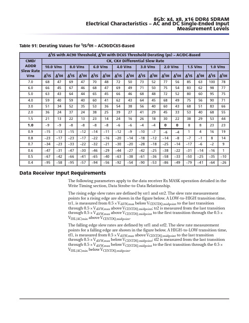
Table 91: Derating Values for t IS/t IH – AC90/DC65-BasedData Receiver Input RequirementsThe following parameters apply to the data receiver Rx MASK operation detailed in theWrite Timing section, Data Strobe-to-Data Relationship.The rising edge slew rates are defined by srr1 and srr2. The slew rate measurementpoints for a rising edge are shown in the figure below. A LOW-to-HIGH transition time,tr1, is measured from 0.5 × V diVW,max below V CENTDQ,midpoint to the last transitionthrough 0.5 × V diVW,max above V CENTDQ,midpoint ; tr2 is measured from the last transitionthrough 0.5 × V diVW,max above V CENTDQ,midpoint to the first transition through the 0.5 ×V IHL(AC)min above V CENTDQ,midpoint .The falling edge slew rates are defined by srf1 and srf2. The slew rate measurementpoints for a falling edge are shown in the figure below. A HIGH-to-LOW transition time,tf1, is measured from 0.5 × V diVW,max above V CENTDQ,midpoint to the last transitionthrough 0.5 × V diVW,max below V CENTDQ,midpoint ; tf2 is measured from the last transitionthrough 0.5 × V diVW,max below V CENTDQ,midpoint to the first transition through the 0.5 ×V IHL(AC)min below V CENTDQ,midpoint .8Gb: x4, x8, x16 DDR4 SDRAM Electrical Characteristics – AC and DC Single-Ended Input Measurement Levels2.Micron recommends calibrating pull-up ODT resistors at 0.8 × V DDQ . Other calibrationschemes may be used to achieve the linearity specification shown here.3.The tolerance limits are specified under the condition that V DDQ = V DD and V SSQ = V SS .4.The DQ-to-DQ mismatch within byte variation for a given component including DQS_tand DQS_c.5.R TT variance range ratio to R TT nominal value in a given component, including DQS_tand DQS_c.DQ-to-DQ mismatch =R TT(MAX) - R TT(MIN)R TT(NOM)× 1006.DQ-to-DQ mismatch for a x16 device is treated as two separate bytes.7.For IT, AT, and UT devices, the minimum values are derated by 9% when the device op-erates between –40°C and 0°C (TC).ODT Temperature and Voltage SensitivityIf temperature and/or voltage change after calibration, the tolerance limits widen ac-cording to the following equations and tables.˂T = T - T(@ calibration); ˂V = V DDQ - V DDQ (@ calibration); V DD = V DDQTable 129: ODT Sensitivity DefinitionsTable 130: ODT Voltage and Temperature SensitivityODT Timing DefinitionsThe reference load for ODT timings is different than the reference load used for timingmeasurements.Figure 241: ODT Timing Reference Load8Gb: x4, x8, x16 DDR4 SDRAM Electrical Characteristics – On-Die Termination Characteristics。
MEMORY存储芯片MT41K512M16TSR-125AIT E中文规格书
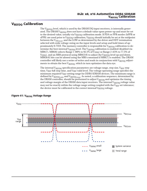
V REFDQ CalibrationThe V REFDQ level, which is used by the DRAM DQ input receivers, is internally gener-ated. The DRAM V REFDQ does not have a default value upon power-up and must be setto the desired value, usually via V REFDQ calibration mode. If PDA or PPR modes (hPPR orsPPR) are used prior to V REFDQ calibration, V REFDQ should initially be set at the midpointbetween the V DD,max , and the LOW as determined by the driver and ODT terminationselected with wide voltage swing on the input levels and setup and hold times of ap-proximately 0.75UI. The memory controller is responsible for V REFDQ calibration to de-termine the best internal V REFDQ level. The V REFDQ calibration is enabled/disabled viaMR6[7], MR6[6] selects Range 1 (60% to 92.5% of V DDQ ) or Range 2 (45% to 77.5% ofV DDQ ), and an MRS protocol using MR6[5:0] to adjust the V REFDQ level up and down.MR6[6:0] bits can be altered using the MRS command if MR6[7] is enabled. The DRAMcontroller will likely use a series of writes and reads in conjunction with V REFDQ adjust-ments to obtain the best V REFDQ , which in turn optimizes the data eye.The internal V REFDQ specification parameters are voltage range, step size, V REF steptime, V REF full step time, and V REF valid level. The voltage operating range specifies theminimum required V REF setting range for DDR4 SDRAM devices. The minimum range isdefined by V REFDQ,min and V REFDQ,max . As noted, a calibration sequence, determined bythe DRAM controller, should be performed to adjust V REFDQ and optimize the timingand voltage margin of the DRAM data input receivers. The internal V REFDQ voltage valuemay not be exactly within the voltage range setting coupled with the V REF set tolerance;the device must be calibrated to the correct internal V REFDQ voltage.Figure 61: V REFDQ Voltage RangeV DDQV REF rangeV SWING smallV SWING large System variance Total rangeV REF ,maxV REF,min8Gb: x8, x16 Automotive DDR4 SDRAM V REFDQ CalibrationWhen the CAL mode is enabled, additional time is required for the MRS command tocomplete. The earliest the next valid command can be issued is t MOD_CAL, whichshould be equal to t MOD + t CAL. The two following figures are examples.Figure 24: CAL Enable Timing – t MOD_CALCK_cCK_tAddress CS_nSettings CommandNote: 1.CAL mode is enabled at T1.Figure 25: t MOD_CAL, MRS to Valid Command Timing with CAL EnabledCK_cCK_tAddress CS_n Settings Command Note: 1.MRS at Ta1 may or may not modify CAL, t MOD_CAL is computed based on new t CAL set-ting if modified.8Gb: x8, x16 Automotive DDR4 SDRAM Command Address Latency。
MEMORY存储芯片MT41J64M16LA-15F B中文规格书
SELF REFRESH OperationThe SELF REFRESH command can be used to retain data in the device, even if the restof the system is powered down. When in self refresh mode, the device retains data with-out external clocking. The device has a built-in timer to accommodate SELF REFRESHoperation. The SELF REFRESH command is defined by having CS_n, RAS_n, CAS_n,and CKE held LOW with WE_n and ACT_n HIGH at the rising edge of the clock.Before issuing the SELF REFRESH ENTRY command, the device must be idle with allbanks in the precharge state and t RP satisfied. Idle state is defined as: All banks areclosed (t RP , t DAL, and so on, satisfied), no data bursts are in progress, CKE is HIGH, andall timings from previous operations are satisfied (t MRD, t MOD, t RFC, t ZQinit, t ZQoper,t ZQCS, and so on). After the SELF REFRESH ENTRY command is registered, CKE mustbe held LOW to keep the device in self refresh mode. The DRAM automatically disablesODT termination, regardless of the ODT pin, when it enters self refresh mode and auto-matically enables ODT upon exiting self refresh. During normal operation (DLL_on),the DLL is automatically disabled upon entering self refresh and is automatically ena-bled (including a DLL reset) upon exiting self refresh.When the device has entered self refresh mode, all of the external control signals, exceptCKE and RESET_n, are “Don’t Care.” For proper SELF REFRESH operation, all powersupply and reference pins (V DD , V DDQ , V SS , V SSQ , V PP , and V REFCA ) must be at valid levels.The DRAM internal V REFDQ generator circuitry may remain on or be turned off depend-ing on the MR6 bit 7 setting. If the internal V REFDQ circuit is on in self refresh, the firstWRITE operation or first write-leveling activity may occur after t XS time after self re-fresh exit. If the DRAM internal V REFDQ circuitry is turned off in self refresh, it ensuresthat the V REFDQ generator circuitry is powered up and stable within the t XSDLL periodwhen the DRAM exits the self refresh state. The first WRITE operation or first write-lev-eling activity may not occur earlier than t XSDLL after exiting self refresh. The device ini-tiates a minimum of one REFRESH command internally within the t CKE period once itenters self refresh mode.The clock is internally disabled during a SELF REFRESH operation to save power. Theminimum time that the device must remain in self refresh mode is t CKESR/t CKESR_PAR. The user may change the external clock frequency or halt the externalclock t CKSRE/t CKSRE_PAR after self refresh entry is registered; however, the clock mustbe restarted and t CKSRX must be stable before the device can exit SELF REFRESH oper-ation.The procedure for exiting self refresh requires a sequence of events. First, the clock mustbe stable prior to CKE going back HIGH. Once a SELF REFRESH EXIT command (SRX,combination of CKE going HIGH and DESELECT on the command bus) is registered,the following timing delay must be satisfied:Commands that do not require locked DLL:•t XS = ACT, PRE, PREA, REF , SRE, and PDE.•t XS_FAST = ZQCL, ZQCS, and MRS commands. For an MRS command, only DRAMCL, WR/RTP register, and DLL reset in MR0; R TT(NOM) register in MR1; the CWL andR TT(WR) registers in MR2; and gear-down mode register in MR3; WRITE and READ pre-amble registers in MR4; R TT(PARK) register in MR5; Data rate and V REFDQ calibrationvalue registers in MR6 may be accessed provided the DRAM is not in per-DRAMmode. Access to other DRAM mode registers must satisfy t XS timing. WRITE com-mands (WR, WRS4, WRS8, WRA, WRAS4, and WRAS8) that require synchronous ODTand dynamic ODT controlled by the WRITE command require a locked DLL.8Gb: x4, x8, x16 DDR4 SDRAM SELF REFRESH OperationREAD Followed by WRITE with CRC EnabledFigure 161: READ (BL8) to WRITE (BL8 or BC4: OTF) with 1t CK Preamble and Write CRC in Same or Different Bank GroupCommand DQ x4,BL = 8CK_t CK_cDQS_t,DQS_cBank GroupAddress Address DQ x8/X16,BL = 8DQ x4,READ: BL = 8,WRITE: BC = 4 (OTF)DQ x8/X16,READ: BL = 8,WRITE: BC = 4 (OTF)Notes: 1.BL = 8 (or BC = 4: OTF for Write), RL = 11 (CL = 11, AL = 0), READ preamble = 1t CK, WL =9 (CWL = 9, AL = 0), WRITE preamble = 1t CK.2.DO n = data-out from column n , DI b = data-in from column b .3.DES commands are shown for ease of illustration; other commands may be valid atthese times.4.BL8 setting activated by either MR0[1:0] = 00 or MR0[1:0] = 01 and A12 = 1 during READcommands at T0 and WRITE commands at T8.5.BC4 setting activated by MR0[1:0] = 01 and A12 = 0 during WRITE commands at T8.6.CA parity = Disable, CS to CA latency = Disable, Read DBI = Disable, Write DBI = Disable,Write CRC = Enable.8Gb: x4, x8, x16 DDR4 SDRAM READ Operation。
MEMORY存储芯片MT41J64M16LA-15EIT B中文规格书

Low-Power Auto Self Refresh ModeAn auto self refresh mode is provided for application ease. Auto self refresh mode is en-abled by setting MR2[6] = 1 and MR2[7] = 1. The device will manage self refresh entry over the supported temperature range of the DRAM. In this mode, the device willchange its self refresh rate as the DRAM operating temperature changes, going lower at low temperatures and higher at high temperatures.Manual Self Refresh ModeIf auto self refresh mode is not enabled, the low-power auto self refresh mode register must be manually programmed to one of the three self refresh operating modes. This mode provides the flexibility to select a fixed self refresh operating mode at the entry of the self refresh, according to the system memory temperature conditions. The user is responsible for maintaining the required memory temperature condition for the mode selected during the SELF REFRESH operation. The user may change the selected mode after exiting self refresh and before entering the next self refresh. If the temperature condition is exceeded for the mode selected, there is a risk to data retention resulting in loss of data.Table 27: Auto Self Refresh Mode8Gb: x4, x8, x16 DDR4 SDRAM Low-Power Auto Self Refresh Mode。
MEMORY存储芯片MT41J64M16JT-15E XIT G中文规格书
3.DES commands are shown for ease of illustration; other commands may be valid atthese times.4.BC4 setting activated by MR0[1:0] = 10.5.CA parity = Disable, CS to CA latency = Disable, Read DBI = Disable, Write DBI = Disable,Write CRC = Disable.6.The write timing parameter (t WTR_L) is referenced from the first rising clock edge afterthe last write data shown at T11.WRITE Operation Followed by PRECHARGE OperationThe minimum external WRITE command to PRECHARGE command spacing is equal toWL (AL + CWL) plus either 4t CK (BL8/BC4-OTF) or 2t CK (BC4-fixed) plus t WR. The min-imum ACT to PRE timing, t RAS, must be satisfied as well.Figure 190: WRITE (BL8/BC4-OTF) to PRECHARGE with 1t CK PreambleCommand DQCK_t CK_cDQS_t,DQS_c AddressDQ DQS_t,DQS_c Notes: 1.BL = 8 with BC4-OTF , WL = 9 (CWL = 9, AL = 0 ), Preamble = 1t CK, t WR = 12.2.DI n = data-in from column n .3.DES commands are shown for ease of illustration; other commands may be valid atthese times.4.BC4 setting activated by MR0[1:0] = 01 and A12 = 0 during WRITE command at T0. BL8setting activated by MR0[1:0] = 00 or MR0[1:0] = 01 and A12 = 1 during WRITE commandat T0.5.CA parity = Disable, CS to CA latency = Disable, Read DBI = Disable, CRC = Disable.6.The write recovery time (t WR) is referenced from the first rising clock edge after the lastwrite data shown at T13. t WR specifies the last burst WRITE cycle until the PRECHARGEcommand can be issued to the same bank.8Gb: x4, x8, x16 DDR4 SDRAM WRITE OperationFigure 146: READ (BC4) OTF to WRITE (BC4) OTF with 2t CK Preamble in Same or Different Bank GroupCommand DQ CK_t CK_cDQS_t,DQS_cBank GroupAddress Address Notes: 1.BC = 4, RL = 11 (CL = 11, AL = 0), READ preamble = 2t CK, WL = 10 (CWL = 9 + 1 [see Note5], AL = 0), WRITE preamble = 2t CK.2.DO n = data-out from column n ; DI b = data-in from column b .3.DES commands are shown for ease of illustration; other commands may be valid atthese times.4.BC4 (OTF) setting activated by MR0[1:0] = 01 and A12 = 0 during READ commands at T0and WRITE commands at T6.5.When operating in 2t CK WRITE preamble mode, CWL may need to be programmed to avalue at least 1 clock greater than the lowest CWL setting.6.CA parity = Disable, CS to CA latency = Disable, Read DBI = Disable, Write DBI = Disable,Write CRC = Disable.Figure 147: READ (BC4) Fixed to WRITE (BC4) Fixed with 1t CK Preamble in Same or Different BankGroupCommand DQCK_t CK_cDQS_t,DQS_cBank GroupAddress Address Notes: 1.BC = 4, RL = 11 (CL = 11, AL = 0), READ preamble = 1t CK, WL = 9 (CWL = 9, AL = 0),WRITE preamble = 1t CK.2.DO n = data-out from column n ; DI b = data-in from column b .8Gb: x4, x8, x16 DDR4 SDRAM READ Operation。
MEMORY存储芯片MT41J256M8HX-15EIT中文规格书
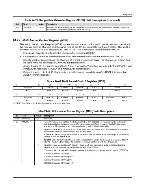
RegistersTable24-28.Sample Rate Generator Register(SRGR)Field Descriptions(continued) Bit Field Value Description7-0CLKGDV0-FFh Sample-rate generator clock(CLKG)divider value is used as the divide-down number to generatethe required sample-rate generator clock frequency.24.3.7Multichannel Control Register(MCR)The multichannel control register(MCR)has control and status bits for multichannel selection operation in the receiver(with an R prefix)and the same type of bits for the transmitter(with an X prefix).The MCR is shown in Figure24-48and described in Table24-29.This I/O-mapped register enables you to:•Enable all channels or only selected channels for reception(RMCM).•Choose which channels are enabled/disabled and masked/unmasked for transmission(XMCM).•Specify whether two partitions(32channels at a time)or eight partitions(128channels at a time)can be used(RMCME for reception,XMCME for transmission).•Assign blocks of16channels to partitions A and B when the2-partition mode is selected(RPABLK and RPBBLK for reception,XPABLK and XPBBLK for transmission).•Determine which block of16channels is currently involved in a data transfer(RCBLK for reception, XCBLK for transmission).Figure24-48.Multichannel Control Registers(MCR) 3126252423222120181716 Reserved XMCME XPBBLK XPABLK XCBLK XMCM R-0R/W-0R/W-0R/W-0R-0R/W-0 1510987654210 Reserved RMCME RPBBLK RPABLK RCBLK Reserved RMCM R-0R/W-0R/W-0R/W-0R-0R-0R/W-0 LEGEND:R=Read only;R/W=Read/Write;-n=value after resetTable24-29.Multichannel Control Register(MCR)Field Descriptions Bit Field Value Description31-26Reserved0Reserved.25XMCME Transmit multichannel partition mode bit.XMCME is only applicable if channels can be individuallydisabled/enabled or masked/unmasked for transmission(XMCM is nonzero).XMCME determineswhether only32channels or all128channels are to be individually selectable.02-partition mode.Only partitions A and B are used.You can control up to32channels in the transmitmultichannel selection mode selected with the XMCM bit.If XMCM=1or2h:assign16channels to partition A with the XPABLK bit and assign16channels topartition B with the XPBBLK bit.If XMCM=3h:(for symmetric transmission and reception),assign16channels to receive partition Awith the RPABLK bit and assign16channels to receive partition B with the RPBBLK bit.18-partition mode.All partitions(A through H)are used.You can control up to128channels in thetransmit multichannel selection mode selected with the XMCM bit.You control the channels with the appropriate enhanced transmit channel enable register(XCERE n):XCERE0:Channels0through31XCERE1:Channels32through63XCERE2:Channels64through95XCERE3:Channels96through127Registers e of the Transmit Channel Enable Registers(continued)Number of selectable channelsBlock Assignments Channel Assignments XCERE n Block assigned(1)Bit inXCERE n Channel assigned(1) XCERE3Block6XCE0Channel96......XCE15Channel111Block7XCE16Channel112......XCE31Channel12724.3.10Pin Control Register(PCR)The serial port is configured via the serial port control register(SPCR)and the pin control register(PCR).The PCR contains McBSP status control bits.The PCR is shown in Figure24-51and described inTable24-34.Figure24-51.Pin Control Register(PCR)3116ReservedR-015141312111098 Reserved Reserved(1)Reserved(1)FSXM FSRM CLKXM CLKRM R-0R/W-0R/W-0R/W-0R/W-0R/W-0R/W-0 76543210 SCLKME Reserved(1)Reserved Reserved FSXP FSRP CLKXP CLKRP R/W-0R-0R/W-0R-0R/W-0R/W-0R/W-0R/W-0 LEGEND:R=Read only;R/W=Rear/Write;-n=value afer reset(1)If writing to this field,always write the default value of0to ensure proper McBSP operation.Table24-34.Pin Control Register(PCR)Field Descriptions Bit Field Value Description31-14Reserved0Reserved.The reserved bit location is always read as0.A value written to this field has no effect.13-12Reserved0Reserved.The reserved bit location is always read as0.A value written to this field has no effect.Ifwriting to this field,always write the default value of0to ensure proper McBSP operation.11FSXM Transmit frame-synchronization mode bit.0Frame-synchronization signal is derived from an external source.1Frame-synchronization signal is determined by FSGM bit in SRGR.10FSRM Receive frame-synchronization mode bit.0Frame-synchronization signal is derived from an external source.FSR is an input pin.1Frame-synchronization signal is generated internally by the sample-rate generator.FSR is an outputpin.9CLKXM Transmit clock mode bit.When CLKSTP bit in SPCR is cleared to0:0CLKX is an input pin and is driven by an external clock.1CLKX is an output pin and is driven by the internal sample-rate generator.。
MEMORY存储芯片MT41J64M16LA-187E IT中文规格书
3. Burst sequence driven on each DQ signal by a READ command. Outside burst operation, DQ signals are VDDQ.
4. For x4 and x8 only.
8Gb: x4, x8, x16 DDR4 SDRAM Ball Descriptions
NC NF
Type I/O
I/O
I/O
Output
Output
Supply Supply Supply Supply Supply Supply Reference
– – –
Description
Data input/output: Bidirectional data bus. DQ represents DQ[3:0], DQ[7:0], and DQ[15:0] for the x4, x8, and x16 configurations, respectively. If write CRC is enabled via mode register, the write CRC code is added at the end of data burst. Any one or all of DQ0, DQ1, DQ2, and DQ3 may be used to monitor the internal VREF level during test via mode register setting MR[4] A[4] = HIGH, training times change when enabled. During this mode, the RTT value should be set to High-Z. This measurement is for verification purposes and is NOT an external voltage supply pin.
MEMORY存储芯片MT41J256M16RE-15ED中文规格书
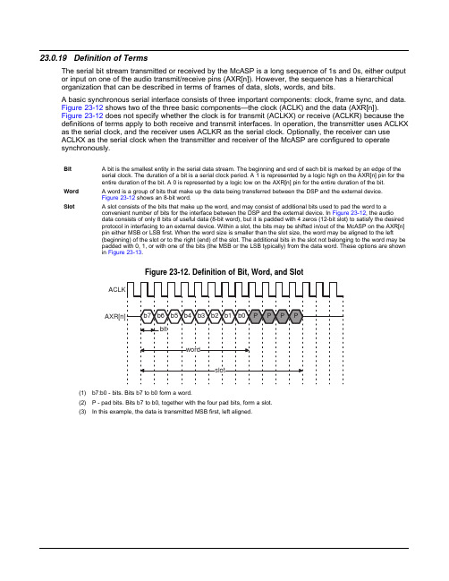
23.0.19Definition of TermsThe serial bit stream transmitted or received by the McASP is a long sequence of1s and0s,either output or input on one of the audio transmit/receive pins(AXR[n]).However,the sequence has a hierarchicalorganization that can be described in terms of frames of data,slots,words,and bits.A basic synchronous serial interface consists of three important components:clock,frame sync,and data.Figure23-12shows two of the three basic components—the clock(ACLK)and the data(AXR[n]).Figure23-12does not specify whether the clock is for transmit(ACLKX)or receive(ACLKR)because the definitions of terms apply to both receive and transmit interfaces.In operation,the transmitter uses ACLKX as the serial clock,and the receiver uses ACLKR as the serial clock.Optionally,the receiver can useACLKX as the serial clock when the transmitter and receiver of the McASP are configured to operatesynchronously.Bit A bit is the smallest entity in the serial data stream.The beginning and end of each bit is marked by an edge of the serial clock.The duration of a bit is a serial clock period.A1is represented by a logic high on the AXR[n]pin for theentire duration of the bit.A0is represented by a logic low on the AXR[n]pin for the entire duration of the bit.Word A word is a group of bits that make up the data being transferred between the DSP and the external device.Figure23-12shows an8-bit word.Slot A slot consists of the bits that make up the word,and may consist of additional bits used to pad the word to a convenient number of bits for the interface between the DSP and the external device.In Figure23-12,the audiodata consists of only8bits of useful data(8-bit word),but it is padded with4zeros(12-bit slot)to satisfy the desiredprotocol in interfacing to an external device.Within a slot,the bits may be shifted in/out of the McASP on the AXR[n]pin either MSB or LSB first.When the word size is smaller than the slot size,the word may be aligned to the left(beginning)of the slot or to the right(end)of the slot.The additional bits in the slot not belonging to the word may bepadded with0,1,or with one of the bits(the MSB or the LSB typically)from the data word.These options are shownin Figure23-13.Figure23-12.Definition of Bit,Word,and Slot(1)b7:b0-bits.Bits b7to b0form a word.(2)P-pad bits.Bits b7to b0,together with the four pad bits,form a slot.(3)In this example,the data is transmitted MSB first,left aligned.23.0.21.2Format UnitThe McASP has two data formatting units,one for transmit and one for receive.These units automatically remap the data bits within the transmitted and received words between a natural format for the DSP(such as a Q31representation)and the required format for the external serial device(such as"I2S format").During the remapping process,the format unit also can mask off certain bits or perform sign extension.Since all transmitters share the same data formatting unit,the McASP only supports one transmit format at a time.For example,the McASP will not transmit in"I2S format"on serializer0,while transmitting"Left Justified"on serializer1.Likewise,the receiver section of the McASP only supports one data format at a time,and this format applies to all receiving serializers.However,the McASP can transmit in one format while receiving in a completely different format.This formatting unit consists of three stages:•Bit mask and pad(masks off bits,performs sign extension)•Rotate right(aligns data within word)•Bit reversal(selects between MSB first or LSB first)Figure23-19shows a block diagram of the receive formatting unit,and Figure23-20shows the transmit formatting unit.Note that the order in which data flows through the three stages is different between the transmit and receive formatting units.Figure23-19.Receive Format UnitParallel read fromXRBUF[n]。
MEMORY存储芯片MT41J128M16HA-15E D中文规格书
Transfer ExamplesFigure16-20.Data Sorting Example PaRAM Configuration(a)EDMA ParametersParameter Contents Parameter00900004h Channel Options Parameter(OPT)40000000h Channel Source Address(SRC)0400h0004h Count for2nd Dimension(BCNT)Count for1st Dimension(ACNT)11800000h Channel Destination Address(DST)0010h0004h Destination BCNT Index(DSTBIDX)Source BCNT Index(SRCBIDX)0000h FFFFh BCNT Reload(BCNTRLD)Link Address(LINK)0004h1000h Destination CCNT Index(DSTCIDX)Source CCNT Index(SRCCIDX)0000h0004h Reserved Count for3rd Dimension(CCNT)(b)Channel Options Parameter(OPT)Content31302827242322212019181716 0000000010010000PRIV Reserved PRIVID ITCCHEN TCCHEN ITCINTEN TCINTEN Reserved TCC151211108743210 0000000000000100 TCC TCCMOD FWID Reserved STATIC SYNCDIM DAM SAMTransfer Examples 16.3.4.4.1Synchronization with the CPUIn order to utilize the ping-pong buffering technique,the system must signal the CPU when to begin toaccess the new data set.After the CPU finishes processing an input buffer(ping),it waits for the EDMA3 to complete before switching to the alternate(pong)buffer.In this example,both channels provide their channel numbers as their report word and set the TCINTEN bit to1to generate an interrupt aftercompletion.When channel3fills an input buffer,the E3bit in the interrupt pending register(IPR)is set to 1;when channel2empties an output buffer,the E2bit in IPR is set to1.The CPU must manually clear these bits.With the channel parameters set,the CPU polls IPR to determine when to switch.The EDMA3 and CPU could alternatively be configured such that the channel completion interrupts the CPU.By doing this,the CPU could service a background task while waiting for the EDMA3to complete.Figure16-28.Ping-Pong Buffering for McBSP Data Example01D0 0004h。
MEMORY存储芯片MT41J64M16LA-187E B中文规格书
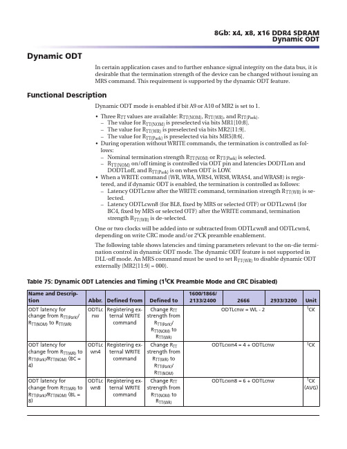
Dynamic ODTIn certain application cases and to further enhance signal integrity on the data bus, it is desirable that the termination strength of the device can be changed without issuing an MRS command. This requirement is supported by the dynamic ODT feature.Functional DescriptionDynamic ODT mode is enabled if bit A9 or A10 of MR2 is set to 1.•Three R TT values are available: R TT(NOM), R TT(WR), and R TT(Park).–The value for R TT(NOM) is preselected via bits MR1[10:8].–The value for R TT(WR) is preselected via bits MR2[11:9].–The value for R TT(Park) is preselected via bits MR5[8:6].•During operation without WRITE commands, the termination is controlled as fol-lows:–Nominal termination strength R TT(NOM) or R TT(Park) is selected.–R TT(NOM) on/off timing is controlled via ODT pin and latencies DODTLon and DODTLoff, and R TT(Park) is on when ODT is LOW.•When a WRITE command (WR, WRA, WRS4, WRS8, WRAS4, and WRAS8) is regis-tered, and if dynamic ODT is enabled, the termination is controlled as follows:–Latency ODTLcnw after the WRITE command, termination strength R TT(WR) is se-lected.–Latency ODTLcwn8 (for BL8, fixed by MRS or selected OTF) or ODTLcwn4 (for BC4, fixed by MRS or selected OTF) after the WRITE command, termination strength R TT(WR) is de-selected.One or two clocks will be added into or subtracted from ODTLcwn8 and ODTLcwn4,depending on write CRC mode and/or 2t CK preamble enablement.The following table shows latencies and timing parameters relevant to the on-die termi-nation control in dynamic ODT mode. The dynamic ODT feature is not supported in DLL-off mode. An MRS command must be used to set R TT(WR) to disable dynamic ODT externally (MR2[11:9] = 000).Table 75: Dynamic ODT Latencies and Timing (1t CK Preamble Mode and CRC Disabled)8Gb: x4, x8, x16 DDR4 SDRAM Dynamic ODT8.The maximum READ preamble is bound by t LZDQS (MIN) on the left side and t DQSCK (MAX) on the right side.Read Timing – Data Strobe-to-Data RelationshipThe data strobe-to-data relationship is shown below and is applied when the DLL is en-abled and locked.Note: t DQSQ: both rising/falling edges of DQS; no t AC defined.Rising data strobe edge parameters:•t DQSQ describes the latest valid transition of the associated DQ pins.•t QH describes the earliest invalid transition of the associated DQ pins.Falling data strobe edge parameters:•t DQSQ describes the latest valid transition of the associated DQ pins.•t QH describes the earliest invalid transition of the associated DQ pins.Data valid window parameters:•t DVWd is the Data Valid Window per device per UI and is derived from [t QH - t DQSQ]of each UI on a given DRAM•t DVWp is the Data Valid Window per pin per UI and is derived [t QH - t DQSQ] of each UI on a pin of a given DRAMFigure 127: Data Strobe-to-Data RelationshipCK_tCK_cCommand 3Address 4DQ 2DQ 2DVWd DVWd T0T1T2T9T10T11T12T13Don’t CareT14T15T16Notes: 1.BL = 8, RL = 11 (AL = 0, CL = 1), Premable = 1t CK.2.D OUT n = data-out from column n .3.DES commands are shown for ease of illustration; other commands may be valid at these times.4.BL8 setting activated by either MR0[A1:0 = 00] or MR0[A1:0 = 01] and A12 = 1 during READ commands at T0.5.Output timings are referenced to V DDQ , and DLL on for locking.6.t DQSQ defines the skew between DQS to data and does not define DQS to clock.8Gb: x4, x8, x16 DDR4 SDRAM READ Operation。
- 1、下载文档前请自行甄别文档内容的完整性,平台不提供额外的编辑、内容补充、找答案等附加服务。
- 2、"仅部分预览"的文档,不可在线预览部分如存在完整性等问题,可反馈申请退款(可完整预览的文档不适用该条件!)。
- 3、如文档侵犯您的权益,请联系客服反馈,我们会尽快为您处理(人工客服工作时间:9:00-18:30)。
DDR3 SDRAMMT41J256M4 – 32 Meg x 4 x 8 banks MT41J128M8 – 16 Meg x 8 x 8 banksMT41J64M16 – 8 Meg x 16 x 8 banksFeatures•V DD = V DDQ = 1.5V ±0.075V•1.5V center-terminated push/pull I/O•Differential bidirectional data strobe•8n-bit prefetch architecture•Differential clock inputs (CK, CK#)•8 internal banks•Nominal and dynamic on-die termination (ODT)for data, strobe, and mask signals•Programmable CAS READ latency (CL)•POSTED CAS ADDITIVE latency (AL)•Programmable CAS WRITE latency (CWL) based ont CK•Fixed burst length (BL) of 8 and burst chop (BC) of 4 (via the mode register set [MRS])•Selectable BC4 or BL8 on-the-fly (OTF)•Self refresh mode•T C of 0°C to 95°C–64ms, 8192 cycle refresh at 0°C to 85°C–32ms, 8192 cycle refresh at 85°C to 95°C•Self refresh temperature (SRT)•Automatic self refresh (ASR)•Write leveling•Multipurpose register•Output driver calibration Options1Marking •Configuration–256 Meg x 4256M4–128 Meg x 8128M8–64 Meg x 1664M16•FBGA package (Pb-free) – x4, x8–78-ball (8mm x 11.5mm) Rev. G JP–78-ball (8mm x 10.5mm) Rev. J DA •FBGA package (Pb-free) – x16–96-ball (8mm x 14mm) Rev. G JT–96-ball (8mm x 14mm) Rev. J TW •Timing – cycle time–938ps @ CL = 14 (DDR3-2133)-093– 1.07ns @ CL = 13 (DDR3-1866)-107– 1.25ns @ CL = 11 (DDR3-1600)-125– 1.5ns @ CL = 9 (DDR3-1333)-15E– 1.87ns @ CL = 7 (DDR3-1066)-187E •Operating temperature–Commercial (0°C ≤ T C≤ +95°C)None–Industrial (–40°C ≤ T C≤ +95°C)IT •Revision:G / :J Note: 1.Not all options listed can be combined todefine an offered product. Use the partcatalog search on for available offerings.Table 1: Key Timing ParametersNotes: 1.Backward compatible to 1066, CL = 7 (-187E).2.Backward compatible to 1333, CL = 9 (-15E).3.Backward compatible to 1600, CL = 11 (-125).4.Backward compatible to 1866, CL = 13 (-107).Table 2: AddressingFigure 1: DDR3 Part NumbersExample Part Number: MT41J256M4DA-107:JNote:1.Not all options listed can be combined to define an offered product. Use the part catalog search on for available offerings.FBGA Part Marking DecoderDue to space limitations, FBGA-packaged components have an abbreviated part marking that is different from the part number. For a quick conversion of an FBGA code, see the FBGA Part Marking Decoder on Micron’s Web site: .Important Notes and WarningsMicron Technology, Inc. ("Micron") reserves the right to make changes to information published in this document,including without limitation specifications and product descriptions. This document supersedes and replaces all information supplied prior to the publication hereof. You may not rely on any information set forth in this docu-ment if you obtain the product described herein from any unauthorized distributor or other source not authorized by Micron.Automotive Applications. Products are not designed or intended for use in automotive applications unless specifi-cally designated by Micron as automotive-grade by their respective data sheets. Distributor and customer/distrib-utor shall assume the sole risk and liability for and shall indemnify and hold Micron harmless against all claims,costs, damages, and expenses and reasonable attorneys' fees arising out of, directly or indirectly, any claim of product liability, personal injury, death, or property damage resulting directly or indirectly from any use of non-automotive-grade products in automotive applications. Customer/distributor shall ensure that the terms and con-ditions of sale between customer/distributor and any customer of distributor/customer (1) state that Micronproducts are not designed or intended for use in automotive applications unless specifically designated by Micron as automotive-grade by their respective data sheets and (2) require such customer of distributor/customer to in-demnify and hold Micron harmless against all claims, costs, damages, and expenses and reasonable attorneys'fees arising out of, directly or indirectly, any claim of product liability, personal injury, death, or property damage resulting from any use of non-automotive-grade products in automotive applications.Critical Applications. Products are not authorized for use in applications in which failure of the Micron compo-nent could result, directly or indirectly in death, personal injury, or severe property or environmental damage ("Critical Applications"). Customer must protect against death, personal injury, and severe property and environ-mental damage by incorporating safety design measures into customer's applications to ensure that failure of the Micron component will not result in such harms. Should customer or distributor purchase, use, or sell any Micron component for any critical application, customer and distributor shall indemnify and hold harmless Micron and its subsidiaries, subcontractors, and affiliates and the directors, officers, and employees of each against all claims,costs, damages, and expenses and reasonable attorneys' fees arising out of, directly or indirectly, any claim of product liability, personal injury, or death arising in any way out of such critical application, whether or not Mi-cron or its subsidiaries, subcontractors, or affiliates were negligent in the design, manufacture, or warning of the Micron product.Customer Responsibility. Customers are responsible for the design, manufacture, and operation of their systems,applications, and products using Micron products. ALL SEMICONDUCTOR PRODUCTS HAVE INHERENT FAIL-URE RATES AND LIMITED USEFUL LIVES. IT IS THE CUSTOMER'S SOLE RESPONSIBILITY TO DETERMINE WHETHER THE MICRON PRODUCT IS SUITABLE AND FIT FOR THE CUSTOMER'S SYSTEM, APPLICATION, OR PRODUCT. Customers must ensure that adequate design, manufacturing, and operating safeguards are included in customer's applications and products to eliminate the risk that personal injury, death, or severe property or en-vironmental damages will result from failure of any semiconductor component.Limited Warranty. In no event shall Micron be liable for any indirect, incidental, punitive, special or consequential damages (including without limitation lost profits, lost savings, business interruption, costs related to the removal or replacement of any products or rework charges) whether or not such damages are based on tort, warranty,breach of contract or other legal theory, unless explicitly stated in a written agreement executed by Micron's duly authorized representative.1Gb: x4, x8, x16 DDR3 SDRAMImportant Notes and WarningsState DiagramFigure 2: Simplified State DiagramSRX = Self refresh exit WRITE = WR, WRS4, WRS8WRITE AP = WRAP , WRAPS4, WRAPS8ZQCL = ZQ LONG CALIBRATION ZQCS = ZQ SHORT CALIBRATIONCommand sequenceACT = ACTIVATEMPR = Multipurpose register MRS = Mode register set PDE = Power-down entry PDX = Power-down exit PRE = PRECHARGE PREA = PRECHARGE ALL READ = RD, RDS4, RDS8READ AP = RDAP , RDAPS4, RDAPS8REF = REFRESHRESET = START RESET PROCEDURE SRE = Self refresh entryFunctional DescriptionDDR3 SDRAM uses a double data rate architecture to achieve high-speed operation.The double data rate architecture is an 8n-prefetch architecture with an interface de-signed to transfer two data words per clock cycle at the I/O pins. A single read or writeoperation for the DDR3 SDRAM effectively consists of a single 8n-bit-wide, four-clock-cycle data transfer at the internal DRAM core and eight corresponding n-bit-wide, one-half-clock-cycle data transfers at the I/O pins.The differential data strobe (DQS, DQS#) is transmitted externally, along with data, foruse in data capture at the DDR3 SDRAM input receiver. DQS is center-aligned with datafor WRITEs. The read data is transmitted by the DDR3 SDRAM and edge-aligned to thedata strobes.The DDR3 SDRAM operates from a differential clock (CK and CK#). The crossing of CKgoing HIGH and CK# going LOW is referred to as the positive edge of CK. Control, com-mand, and address signals are registered at every positive edge of CK. Input data is reg-istered on the first rising edge of DQS after the WRITE preamble, and output data is ref-erenced on the first rising edge of DQS after the READ preamble.Read and write accesses to the DDR3 SDRAM are burst-oriented. Accesses start at a se-lected location and continue for a programmed number of locations in a programmedsequence. Accesses begin with the registration of an ACTIVATE command, which is thenfollowed by a READ or WRITE command. The address bits registered coincident withthe ACTIVATE command are used to select the bank and row to be accessed. The ad-dress bits registered coincident with the READ or WRITE commands are used to selectthe bank and the starting column location for the burst access.The device uses a READ and WRITE BL8 and BC4. An auto precharge function may beenabled to provide a self-timed row precharge that is initiated at the end of the burstaccess.As with standard DDR SDRAM, the pipelined, multibank architecture of DDR3 SDRAMallows for concurrent operation, thereby providing high bandwidth by hiding row pre-charge and activation time.A self refresh mode is provided, along with a power-saving, power-down mode. Industrial TemperatureThe industrial temperature (IT) device requires that the case temperature not exceed–40°C or 95°C. JEDEC specifications require the refresh rate to double when T C exceeds85°C; this also requires use of the high-temperature self refresh option. Additionally,ODT resistance and the input/output impedance must be derated when T C is < 0°C or>95°C.General Notes•The functionality and the timing specifications discussed in this data sheet are for theDLL enable mode of operation (normal operation).•Throughout this data sheet, various figures and text refer to DQs as “DQ.” DQ is to beinterpreted as any and all DQ collectively, unless specifically stated otherwise.•The terms “DQS” and “CK” found throughout this data sheet are to be interpreted asDQS, DQS# and CK, CK# respectively, unless specifically stated otherwise.•Complete functionality may be described throughout the document; any page or dia-gram may have been simplified to convey a topic and may not be inclusive of all re-quirements.•Any specific requirement takes precedence over a general statement.•Any functionality not specifically stated is considered undefined, illegal, and not sup-ported, and can result in unknown operation.•Row addressing is denoted as A[n:0]. For example, 1Gb: n = 12 (x16); 1Gb: n = 13 (x4, x8); 2Gb: n = 13 (x16) and 2Gb: n = 14 (x4, x8); 4Gb: n = 14 (x16); and 4Gb: n = 15 (x4, x8).•Dynamic ODT has a special use case: when DDR3 devices are architected for use in a single rank memory array, the ODT ball can be wired HIGH rather than routed. Refer to the Dynamic ODT Special Use Case section.•A x16 device's DQ bus is comprised of two bytes. If only one of the bytes needs to be used, use the lower byte for data transfers and terminate the upper byte as noted:–Connect UDQS to ground via 1kΩ* resistor.–Connect UDQS# to V DD via 1kΩ* resistor.–Connect UDM to V DD via 1kΩ* resistor.–Connect DQ[15:8] individually to either V SS, V DD, or V REF via 1kΩ resistors,* or float DQ[15:8].*If ODT is used, 1kΩ resistor should be changed to 4x that of the selected ODT.Functional Block DiagramsDDR3 SDRAM is a high-speed, CMOS dynamic random access memory. It is internallyconfigured as an 8-bank DRAM.Figure 3: 256 Meg x 4 Functional Block DiagramFigure 4: 128 Meg x 8 Functional Block DiagramFigure 5: 64 Meg x 16 Functional Block Diagram。