DT-2R722-A7;中文规格书,Datasheet资料
TMDSDCDCLEDKIT;中文规格书,Datasheet资料

Quick Start GuideSPRUGV0–May2010 TMS320C2000™DC/DC LED Lighting Developer's KitQuick Start GuideThis document provides instructions to run a GUI that controls the DC/DC LED Lighting Developer’s Kit board using the Piccolo F28035microcontroller.Contents of the DC/DC LED Lighting Developer’s Kit include:•DC/DC LED Lighting power board•Piccolo F28035controlCARD.•LED panel•12V power adapter•Banana Plug Cable•USB Cable•USB drive with GUI executable•CCS4Installation CDFeatures of the DC/DC LED Lighting Developer’s Kit include:•Independent closed-loop brightness control of eight LED strings(six strings included with kit)with PWM dimming•Closed-loop voltage control of the LED bus using a shared SEPIC stage•On-board isolated JTAG emulation•Over-current and over-voltage protection for the SEPIC stage using the F28x trip-zone(TZ)submodule •UART communication available for host-control•Hardware Developer’s Package is available and includes schematics,bill of materials,Gerber files,etc. 1OverviewThe DC/DC LED Lighting Developer’s Kit uses a12to36V DC input.This voltage is then regulated to a different level by a SEPIC converter.SEPIC,as a buck-boost topology,is able to increase or decrease the input voltage.For our application,we will be setting the SEPIC output voltage to approximately20V,independent of the board input.The SEPIC output is then connected to each of the LED strings.To1 SPRUGV0–May2010TMS320C2000™DC/DC LED Lighting Developer's Kit Quick Start GuideDC12-Overview perform independent LED string dimming,a MOSFET is placed in series with each string,and the on-time of this string’s MOSFET will control the average current through an LED string.Since the brightness of an LED is roughly proportional to the LED current,we use the duty cycle of each string’s PWM to control the average current drawn.The figure below illustrates the hardware that is present on the DC/DC LEDLighting Developer’s Kit.A typical power conversion board is made up of several power stages.On the Lighting_DCDC board,each of these power stages takes the form of a macro section.Each of these macro sections is bounded by its own silkscreen area.Below is a list of all the macro blocks’names and a short description of theirfunctions.Refer to the image on the next page for placement of macro areas.Lighting_DCDC Main Board -Consists of a controlCARD socket,a few communications jumpers,[Main]and the routing of signals between the controlCARD and the macroblocks.This section includes all of the area outside of the macroblocks.DC-PwrEntry Macro –[M1]Generates the 15V,5V,and 3.3V DC rails from a 12V supplyincluded with the kit or an external DC power supply.Isolated-USB-to-JTAG Macro –Provides on-board isolated JTAG connection through USB to the[M2]host.It is also used to provide isolated SCI (UART)communicationfor connection with the GUI.SEPIC-LV Macro –[M3]A SEPIC DC/DC conversion stage,used to increase or decrease theinput voltage to the voltage needed by the LED strings.LED-dimming Macro –[M4]-[M7]Stages used to individually dim an LED string.Each macro consistsof the components needed to control two strings.In this guide,each component is named first with its macro number,followed by the reference name.For example,[M2]-J1would refer to the jumper J1located in the macro M2,and [Main]-J1would refer to theJ1located on the board outside of the other defined macro blocks.2TMS320C2000™DC/DC LED Lighting Developer's Kit Quick Start GuideSPRUGV0–May 2010[Main]-J6EmulationEnable/DisableJumper [Main]-BS2Sepic Out Connector[M1]-JP1 12V Input Connector[M1]-J1JP1=DcBusEnable/Disable [M1]-TB1External DCSupply (not used)[M1]-SW1Main PowerSwitch [M2]-JP1 USBEmulatorConnector [Main]-BS3LED Bus ConnectorM7M6M5M4M2 Quick Start GUI 2Quick Start GUIThis kit comes with a GUI which provides a convenient way to evaluate the functionality of this kit and the F28035device,without having to learn and configure the underlying project software or install CodeComposer Studio™.The interactive interface using sliders,buttons,and text boxes,allows LED lighting with the C2000device to be demonstrated quickly and easily.2.1Hardware SetupListed below are some of the major connectors and features of the DC/DC LED Lighting board.Step 1.On the Piccolo F28035controlCARD,check the following switches:•SW1,make sure this switch is in the “OFF”(down)position •SW2,make sure position 1and 2are both in the “ON”(up)position Step 2.Put a F28035control card into the socket on the LED Lighting board,and connect a cablefrom the USB connector on the board to the computer.[M2]-LD1,near the LED Lightingboard’s USB connector,should turn on.3SPRUGV0–May 2010TMS320C2000™DC/DC LED Lighting Developer's Kit Quick Start GuideQuick Start GUI On the next screen select“Install from specific location”Click next and the drivers will be installed.The driver install screen will appearthree times,repeat this procedure each time.Step3.Connect the LED panel to the LED Lighting board via[Main]-TB1to TB8.Step4.Connect of verify the following:•Connect a jumper on[M1]-J1•Connect a jumper on[M2]-J4•Remove any jumpers placed on[Main]-J6Step5.Connect the banana-to-banana plug wire that came with the kit between the SEPIC-out Connector(BS2)and the LED Bus connector(BS3).Step6.Place[M1]-SW2into the"OFF"position.This switch will not be used in this demonstration.Step7.Connect a12V power supply to power up to[M1]-JP1of the board.Turn[M1]-SW1to the "ON"position.When on,[M1]-LD1and[M1]-LD2should turn on.2.2Software SetupThe GUI used to conveniently evaluate the kit can be found on the USB drive that is included with this kit.It is named Lighting_DCDC.exe.This.exe contains all the software necessary to do a quick evaluation of this kit.To explore deeper,the underlying reference software can be found as a Code Composer Studio project within controlSUITE.NOTE:The GUI requires framework3.0to run.Please ensure that this software isinstalled prior to running this program.•To install the CCS4project built to run with this kit,use the most up-to-date software,and find all reference software for the C2000MCU.Please install controlSUITE which can be downloaded at:/controlSUITE•Once controlSUITE is installed,the GUI mentioned in this guide can be found at the following location:c controlSUITE/development_kits/Lighting_DCDC_vX.X/~GUI/Lighting_DCDC.exe4TMS320C2000™DC/DC LED Lighting Developer's Kit Quick Start Guide SPRUGV0–May2010 Quick Start GUI •The source code for this GUI was written in C#using Microsoft Visual and can be found at:controlSUITE/development_kits/Lighting_DCDC_vX.X/~GUI/~Source/•The kit ships with a F28035controlCARD that has been pre-flashed with the code that enables it to run with the GUI that comes with this kit.If for any reason,the software needs to be reflashed so that itworks with the GUI again,this flash image can be found at:controlSUITE/development_kits/Lighting_DCDC_vX.X/~GUI/Lighting_DCDC-FlashImage_v1.0.out •The underlying Code Composer Studio4project documentation and how to run guide can be found at: controlSUITE/development_kits/Lighting_DCDC_vX.X/Lighting_DCDC/~Docs/Lighting_DCDC.pdf2.3Running the GUIThe following steps will allow you to run the GUI:1.Browse to and double-click on Lighting_DCDC.exe.If this is the first time that the GUI is run,the GUIwill ask the user to read a license agreement.Assuming that the license is accepted,the image belowwill be seen:2.Click“Setup Connection”on the GUI and ensure the Baud Rate is set to57600and that the“Boot onConnect”box is unchecked.3.Next you will need to select your serial comport.This can be found by going to:Control Panel->System->Hardware tab->Device Manager->Ports(COM&LPT)Look for the comport that is named“USB Serial Port”or similar,then select this comport in the“SetupConnection”window.4.Click“OK.”This will close the“Setup Connection”window.5.Turn on the board by switching[M1]-SW1to the“ON”position.6.On the Main Window,click“Connect.”When connected,the status bar at the bottom left of the GUIshould say“Connected.”5 SPRUGV0–May2010TMS320C2000™DC/DC LED Lighting Developer's Kit Quick Start GuideReferences 7.Move the“Sepic Output”slider to approximately20V.This sets the reference to which the controllerwill try to regulate the output of the Sepic.8.Change the value of LED string1’s target current to0.04A.Note that the“LED String1Current”rampsuntil it reaches approximately0.04A.9.Edit the other strings’target currents as desired.Note that the average LED current draw isproportional to LED lumen output for most high brightness LEDs.Therefore,in this program,thebrightness of the LEDs is being controlled.NOTE:Near the bottom of the GUI there is a checkbox control named“Merge LED controls.”Thiscontrol enables/disables individual control of each LED string and has the controller try andoutput the same current for each string.This reference is set by a slider.NOTE:There will be some variation from LED to LED from0.0to approximately0.02A.This isbecause the LEDs used are not guaranteed,from the manufacturer,to be identical until theLED current is greater than0.05A.10.When finished,set the“Sepic Output”to0V then click“Disconnect.”11.Power off the board by switching[M1]-SW1to the"OFF"position.3ReferencesFor more information,please see the following guides:•Lighting_DCDC–provides detailed information on the CCS4Lighting_DCDC project within an easy to use lab-style format.C:\TI\controlSUITE\development_kits\Lighting_DCDC_vX.X\Lighting_DCDC\~Docs\Lighting_DCDC.pdf •Lighting_DCDC-HWdevPkg–a folder containing various files related to the hardware on the Motor Control and PFC Developer’s Kit board(schematics,bill of materials,Gerber files,PCB layout,etc).C:\TI\controlSUITE\development_kits\Lighting_DCDC_vX.X\~Lighting_DCDC-HwdevPkg\•Lighting_DCDC-HWGuide–presents full documentation on the hardware found on the Lighting_DCDC board.C:\TI\controlSUITE\development_kits\Lighting_DCDC_vX.X\~Docs\Lighting_DCDC-HWGuide.pdf6TMS320C2000™DC/DC LED Lighting Developer's Kit Quick Start Guide SPRUGV0–May2010IMPORTANT NOTICETexas Instruments Incorporated and its subsidiaries(TI)reserve the right to make corrections,modifications,enhancements,improvements, and other changes to its products and services at any time and to discontinue any product or service without notice.Customers should obtain the latest relevant information before placing orders and should verify that such information is current and complete.All products are sold subject to TI’s terms and conditions of sale supplied at the time of order acknowledgment.TI warrants performance of its hardware products to the specifications applicable at the time of sale in accordance with TI’s standard warranty.Testing and other quality control techniques are used to the extent TI deems necessary to support this warranty.Except where mandated by government requirements,testing of all parameters of each product is not necessarily performed.TI assumes no liability for applications assistance or customer product design.Customers are responsible for their products and applications using TI components.To minimize the risks associated with customer products and applications,customers should provide adequate design and operating safeguards.TI does not warrant or represent that any license,either express or implied,is granted under any TI patent right,copyright,mask work right, or other TI intellectual property right relating to any combination,machine,or process in which TI products or services are rmation published by TI regarding third-party products or services does not constitute a license from TI to use such products or services or a warranty or endorsement e of such information may require a license from a third party under the patents or other intellectual property of the third party,or a license from TI under the patents or other intellectual property of TI.Reproduction of TI information in TI data books or data sheets is permissible only if reproduction is without alteration and is accompanied by all associated warranties,conditions,limitations,and notices.Reproduction of this information with alteration is an unfair and deceptive business practice.TI is not responsible or liable for such altered rmation of third parties may be subject to additional restrictions.Resale of TI products or services with statements different from or beyond the parameters stated by TI for that product or service voids all express and any implied warranties for the associated TI product or service and is an unfair and deceptive business practice.TI is not responsible or liable for any such statements.TI products are not authorized for use in safety-critical applications(such as life support)where a failure of the TI product would reasonably be expected to cause severe personal injury or death,unless officers of the parties have executed an agreement specifically governing such use.Buyers represent that they have all necessary expertise in the safety and regulatory ramifications of their applications,and acknowledge and agree that they are solely responsible for all legal,regulatory and safety-related requirements concerning their products and any use of TI products in such safety-critical applications,notwithstanding any applications-related information or support that may be provided by TI.Further,Buyers must fully indemnify TI and its representatives against any damages arising out of the use of TI products in such safety-critical applications.TI products are neither designed nor intended for use in military/aerospace applications or environments unless the TI products are specifically designated by TI as military-grade or"enhanced plastic."Only products designated by TI as military-grade meet military specifications.Buyers acknowledge and agree that any such use of TI products which TI has not designated as military-grade is solely at the Buyer's risk,and that they are solely responsible for compliance with all legal and regulatory requirements in connection with such use. TI products are neither designed nor intended for use in automotive applications or environments unless the specific TI products are designated by TI as compliant with ISO/TS16949requirements.Buyers acknowledge and agree that,if they use any non-designated products in automotive applications,TI will not be responsible for any failure to meet such requirements.Following are URLs where you can obtain information on other Texas Instruments products and application solutions:Products ApplicationsAmplifiers Audio /audioData Converters Automotive /automotiveDLP®Products Communications and /communicationsTelecomDSP Computers and /computersPeripheralsClocks and Timers /clocks Consumer Electronics /consumer-appsInterface Energy /energyLogic Industrial /industrialPower Mgmt Medical /medicalMicrocontrollers Security /securityRFID Space,Avionics&/space-avionics-defenseDefenseRF/IF and ZigBee®Solutions /lprf Video and Imaging /videoWireless /wireless-appsMailing Address:Texas Instruments,Post Office Box655303,Dallas,Texas75265Copyright©2010,Texas Instruments Incorporated分销商库存信息: TI TMDSDCDCLEDKIT。
三鼎光电sts-722说明书

目录前言 (1)一、仪器各部件名称及其功能 (5)1.1 各部件名称 (5)1.2 显示屏 (7)1.3 键盘 (8)1.4 固定键 (8)1.5 软按键(功能键) (9)1.6 符号 (10)1.7 图标 (10)1.8 菜单树 (11)二、测量前的准备 (12)2.1 仪器开箱和存放 (12)2.2 安置仪器 (12)2.3 电池电量信息 (14)2.4 反射棱镜 (15)2.5 基座的装卸 (15)2.6 望远镜目镜调整和目标照准 (16)2.7 输入模式 (16)2.7.1 输入字符 (17)2.7.2 编辑字符 (18)2.7.3 删除字符 (19)2.8 点搜索 (19)2.9 通配符搜索 (22)三、★星号键功能 (23)3.1 常用设置 (23)3.2 补偿状态 (24)3.3 EDM设置 (24)3.3.1 设置EDM模式 (24)3.3.2 设置目标类型 (25)3.3.3 设置棱镜常数 (25)3.3.4 设置气象数据 (26)3.3.5 格网因子的设置 (28)3.3.6设置仪器常数 (29)3.3.7 查看测距信号 (30)3.4 作业设置 (31)3.4.1 作业文件 (32)3.4.2 调用文件 (32)四、基本测量 (34)4.1 测量注意事项 (34)4.2 基本测量界面 (35)4.3 设置测站点 (36)4.4 定向设置 (38)4.5 数据采集 (41)4.5.1 测存 (43)4.5.2测量 (44)4.5.3 存储 (45)4.5.4编码(调用和添加) (46)4.5.5查看 (46)4.5.6 距离和角度偏心设置 (47)4.6 水平角设置功能 (48)4.7 放样 (49)4.7.1 极坐标法 (50)4.7.2输入放样点 (52)4.7.3从作业中提取坐标 (53)4.7.4 极坐标放样 (54)4.7.5正交法放样 (56)4.7.6 坐标差放样 (58)4.8 系统信息 (60)4.8.1日期和时间设置 (60)五、应用程序 (62)5.1 后方交会 (63)5.2 悬高测量 (66)5.3 对边测量 (69)5.3.1折线对边(A-B,B-C) (69)5.3.2射线对边(A-B,A-C) (71)5.4 面积测量 (73)5.5 道路 (76)5.5.1 道路设计 (76)5.5.1.1编辑水平定线 (77)5.5.1.2修改水平定线 (84)5.5.1.3编辑垂直定线 (85)5.5.1.4修改垂直定线 (86)5.5.1.5删除水平定线 (87)5.5.1.6删除垂直定线 (88)5.5.2道路放样 (88)5.5. 3 斜坡放样 (94)六、文件管理 (97)6.1 测量文件 (98)6.2 坐标文件 (99)6.3 编码.文件 (101)6.4 磁盘信息 (102)6.5 文件导入 (103)6.6 文件导出 (105)6.7 读卡器模式 (107)七、系统设置 (108)八、误差校准 (112)8.1 管水准器 (112)8.2 圆水准器 (112)8.3 望远镜分划板 (113)8.4 竖盘指标零点自动补偿 (114)8.5 指标差( i 角)和竖盘指标零点设置 (114)8.6 视准差(视准轴与横轴的垂直度(2C)) (116)8.7横轴误差的校准 (118)8.8 误差信息 (120)8.9 光学对中器 (120)8.10 仪器常数(K) (121)8.11 视准轴与发射电光轴的平行度 (123)8.12 无棱镜测距 (124)8.13 基座脚螺旋 (124)8.14 反射镜有关组合件 (124)九、技术参数 (126)十、附件 (128)【附录A】计算道路定线元素 (129)1、道路定线元素 (129)2、计算道路定线元素 (131)非常感谢您选购三鼎STS720系列全站仪!本手册使用范围:适用于STS720系列全站仪。
FMB2222A;中文规格书,Datasheet资料
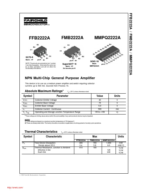
Thermal Characteristics
Symbol
PD RθJA
TA = 25°C unless otherwise noted
Characteristic
Total Device Dissipation Derate above 25°C Thermal Resistance, Junction to Ambient Effective 4 Die Each Die FFB2222A 300 2.4 415
*Pulse Test: Pulse Width ≤ 300 µs, Duty Cycle ≤ 2.0%
Spice Model
NPN (Is=14.34f Xti=3 Eg=1.11 Vaf=74.03 Bf=255.9 Ne=1.307 Ise=14.34f Ikf=.2847 Xtb=1.5 Br=6.092 Nc=2 Isc=0 Ikr=0 Rc=1 Cjc=7.306p Mjc=.3416 Vjc=.75 Fc=.5 Cje=22.01p Mje=.377 Vje=.75 Tr=46.91n Tf=411.1p Itf=.6 Vtf=1.7 Xtf=3 Rb=10)
300
VCE(sat) VBE(sat)
Collector-Emitter Saturation Voltage* Base-Emitter Saturation Voltage*
0.3 1.0 1.2 2.0
V V V V
SMALL SIGNAL CHARACTERISTICS
fT Cobo Cibo NF Current Gain - Bandwidth Product Output Capacitance Input Capacitance Noise Figure IC = 20 mA, VCE = 20 V, f = 100 MHz VCB = 10 V, IE = 0, f = 100 kHz VEB = 0.5 V, IC = 0, f = 100 kHz IC = 100 µA, VCE = 10 V, RS = 1.0 kΩ, f = 1.0 kHz 300 4.0 20 2.0 MHz pF pF dB
1A6(Won-Top Electronics)中文数据手册「EasyDatasheet」
1A1 – 1A71.0A 标准二极管特征!!!!!扩散结低正向压降高电流能力高可靠性高浪涌电流能力A B A机械数据!!!!!!!案例:R-1,模压塑料终端:每焊镀信息MIL-STD-202,方法208极性:阴极频带重量:0.181克(约)安装位置:任意标记:型号数量无铅:对于符合RoHS /无铅版本,新增"-LF"后缀型号,见第4页DR-1Dim Min Max 20.0—A 2.90 3.50B 0.530.64C 2.202.60D在毫米所有尺寸C最大额定值和电气特性单相,半波,60赫兹,电阻或电感性负载.对于容性负载,减免电流20%.@T = 25°C 除非另有说明特有峰值重复反向电压工作峰值反向电压阻断电压DCRM S 反向电压平均整流输出电流(注1)@T = 75°C非重复性峰值正向浪涌电流8.3ms 单半正弦波叠加额定负荷(JEDEC 方法)正向电压峰值反向电流在额定阻断电压DC @I = 1.0A @T = 25°C @T = 100°C符V RRM V RWM V R V R(RM S)I O 1A11A21A31A41A51A61A7Unit 5035100702001404002801.06004208005601000700V V A I FSMV FM I RM C j R J A T j T ST G301.05.0501550-65到+125-65到+150A V µA pF °C/W °C °C典型结电容(注2)典型热阻结到环境(注1)工作温度范围存储温度范围注意:防护持在环境温度下1信息在从情况下距离9.5毫米.2.测4.0V DC 应用反向电压为1.0 M Hz 和1A 1 – 1A 71 of 4I(AV),平均正向整流电流(A )1.0I F ,正向电流(A )100.81.00.60.40.10.20406080100120140160180T A ,环境温度(℃)图. 1正向电流降额曲线0.010.60.8 1.0 1.2 1.4 1.6V F ,正向电压(V )图. 2典型正向特性50100T = 25ºCf = 1MHzIFSM ,峰值正向浪涌电流(A )4030Cj ,电容(pF )8.3ms Single half sine-w aveJEDEC M ethod1020100 1.010循环次数为60 Hz图. 3最大非重复性峰值正向浪涌电流1001.01.010V R ,反向电压(V )图. 4典型结电容1001A 1 – 1A 72 of 4标识信息带卷0.8mm M AX5mm1斧阴极1A x x=极性带=设备号= 1,2,3,4,5,6或71.2mm M AX6mm52.4mm Cathode T ape: Red Anode T ape: White0.8mm M AX封装信息带盒带卷产品ID 标签150mm检查孔(两端)330mm255mm 75mmBULK80±5mm20mm198mm产品ID 标签84mm包装带卷带盒BULK卷轴直径/箱尺寸(mm )330255 x 75 x 150198 x 84 x 20数量(PCS)5,0005,0001,000外箱尺寸(mm)370 x 370 x 420400 x 273 x 415459 x 214 x 256数量(PCS)25,00050,00050,000约.总重量(KG)9.020.018.5Note:1. Paper reel, white or gray color. Core material: plas tic or metal.2. Components are pack ed in accordance with EIA s tandard RS-296-E.1A 1 – 1A 73 of 4订购信息产品编号1A 1-T31A1-TB 1A 11A 2-T31A2-TB 1A 21A 3-T31A3-TB 1A 31A 4-T31A4-TB 1A 41A 5-T31A5-TB 1A 51A 6-T31A6-TB 1A 61A 7-T31A7-TB 1A 71.2.3.封装类型R-1R-1R-1R-1R-1R-1R-1R-1R-1R-1R-1R-1R-1R-1R-1R-1R-1R-1R-1R-1R-1出货数量5000 /磁带和卷轴5000 /带盒1000单位/箱5000 /磁带和卷轴5000 /带盒1000单位/箱5000 /磁带和卷轴5000 /带盒1000单位/箱5000 /磁带和卷轴5000 /带盒1000单位/箱5000 /磁带和卷轴5000 /带盒1000单位/箱5000 /磁带和卷轴5000 /带盒1000单位/箱5000 /磁带和卷轴5000 /带盒1000单位/箱Products lis ted in bold are W TE Preferred devices .Shipping quantity given is for minimum pack ing quantity only. For minimum order quantity, pleas e cons ult the Sales Department.T o order RoHS / Lead Free version (with Lead Free finish), add “-LF” suffix to part number above. For example, 1A1-T B-LF.W on-Top Electronics Co., Ltd (W TE) has check ed all information carefully and believes it to be correct and accurate. However, W TE cannot as s ume any res pons ibility for inaccuracies . Furthermore, this information does not give the purchas er of s emiconductor devices any licens e under patent rights to manufacturer. W TE res erves the right to change any or all information herein without further notice.WARNING:DO NOT USE IN LIFE SUPPORT EQUIPMENT.W TE power s emiconductor products are not authorized for us e as critical components in lifes upport devices or s ys tems without the expres s written approval.1A 1 – 1A 74 of 4。
2N7002K,215;中文规格书,Datasheet资料

2N7002KTrenchMOS™ logic level FETRev. 01 — 20 October 2003Product dataM3D0881.Product profile1.1DescriptionN-channel enhancement mode field-effect transistor in a plastic package using TrenchMOS™ technology.1.2Features1.3Applications1.4Quick reference data2.Pinning informations Logic level compatible s Very fast switchings Subminiature surface mount package s Gate-source ESD protection diodes.s Relay drivers High speed line driver.s V DS ≤60V s I D ≤340mA s P tot ≤0.83Ws R DSon ≤3.9Ω.Table 1:Pinning - SOT23, simplified outline and symbolPin Description Simplified outlineSymbol1gate (g)SOT232source (s)3drain (d)MSB003Top view123gds03ab603.Ordering informationTable 2:Ordering informationType number PackageName Description Version2N7002K SOT23Plastic surface mounted package; 3 leads.SOT23 4.Limiting valuesTable 3:Limiting valuesIn accordance with the Absolute Maximum Rating System (IEC 60134).Symbol Parameter Conditions Min Max Unit V DS drain-source voltage (DC)25°C≤T j≤150°C-60VV DGR drain-gate voltage (DC)25°C≤T j≤150°C; R GS=20kΩ-60VV GS gate-source voltage (DC)-±15VI D drain current (DC)T sp=25°C; V GS=10V;Figure2and3-340mAT sp=100°C; V GS=10V;Figure2-215mA I DM peak drain current T sp=25°C; pulsed; t p≤10µs;Figure3-680mA P tot total power dissipation T sp=25°C;Figure1-0.83W T stg storage temperature−65+150°C T j junction temperature−65+150°C Source-drain diodeI S source (diode forward) current (DC)T sp=25°C-340mA I SM peak source (diode forward) current T sp=25°C; pulsed; t p≤10µs-680mA Electrostatic discharge voltageV esd electrostatic discharge voltage Human Body Model1; C=100pF; R=1.5kΩ-1kVFig 1.Normalized total power dissipation as afunction of solder point temperature.Fig 2.Normalized continuous drain current as afunction of solder point temperature.T sp =25°C; I DM is single pulse; V GS =10VFig 3.Safe operating area; continuous and peak drain currents as a function of drain-source voltage.03aa1704080120050100150200(%)T sp (°C)P der 03aa2504080120050100150200T sp (°C)I der (%)P der P totP tot 25C °()-----------------------100%×=I der I DI D 25C °()-------------------100%×=03an6610-210-11110102V DS (V)I D (A)DC100 ms10 msLimit R DSon = V DS / I D1 mst p = 10 µs100 µs5.Thermal characteristics5.1Transient thermal impedanceTable 4:Thermal characteristicsSymbol ParameterConditionsMin Typ Max Unit R th(j-sp)thermal resistance from junction to solder point Figure 4--150K/W R th(j-a)thermal resistance from junction to ambientminimum footprint;mounted on a printed-circuit board-350-K/WFig 4.Transient thermal impedance from junction to solder point as a function of pulse duration.03aa3911010210310-510-410-310-210-1110t p (s)Z th(j-sp)(K/W)single pulseδ = 0.50.20.10.050.02t pt p TPtTδ =6.CharacteristicsTable 5:CharacteristicsT j=25°C unless otherwise specified.Symbol Parameter Conditions Min Typ Max Unit Static characteristicsV(BR)DSS drain-source breakdown voltage I D=10µA; V GS=0VT j=25°C6075-VT j=−55°C55--VV(BR)GSS drain-source breakdown voltage I G=±1mA; V DS=0V1622-VV GS(th)gate-source threshold voltage I D=1mA; V DS=V GS;Figure9VT j=25°C12-VT j=150°C0.6--VT j=−55°C-- 3.5VI DSS drain-source leakage current V DS=48V; V GS=0VT j=25°C-0.011µAT j=150°C--10µA I GSS gate-source leakage current V GS=±10V; V DS=0V-50500nA R DSon drain-source on-state resistance V GS=10V; I D=500mA;Figure7and8T j=25°C- 2.8 3.9ΩT j=150°C- 5.27.2ΩV GS=4.5V; I D=200mA;Figure7and8- 3.8 5.3ΩDynamic characteristicsC iss input capacitance V GS=0V; V DS=10V; f=1MHz;Figure11-1340pFC oss output capacitance-830pF C rss reverse transfer capacitance-410pFt on turn-on time V DD=50V; R L=250Ω;V GS=10V;R G=50Ω; R GS=50Ω-310nst off turn-off time-915ns Source-drain diodeV SD source-drain (diode forward) voltage I S=300mA; V GS=0V;Figure12-0.93 1.5Vt rr reverse recovery time I S=300mA; dI S/dt=−100A/µs;V GS=0V; V R=25V -30-nsQ r recovered charge-30-nCT j =25°C T j =25°C and 150°C; V DS >I D x R DSonFig 5.Output characteristics: drain current as afunction of drain-source voltage;typical values.Fig 6.Transfer characteristics: drain current as afunction of gate-source voltage; typical values.T j =25°CFig 7.Drain-source on-state resistance as a functionof drain current; typical values.Fig 8.Normalized drain-source on-state resistance factor as a function of junction temperature.03an7000.10.20.30.40.500.511.52V DS (V)I D (A) 3.5 VT j = 25 °CV GS = 10V4 V4.5 V3 V6 V03an7200.10.20.30.40.50246V GS (V)I D (A)V DS > I D x R DSonT j = 25 °C150 °C03an71024681000.10.20.30.40.5I D (A)R DSon (Ω)V GS = 3.5 VT j = 25 °C4.5 V4 V10 V6 V 03aa2800.61.21.82.4-6060120180a T j (°C)a RDSon R DSon 25C °()----------------------------=I D =1mA; V DS =V GS T j =25°C; V DS =5VFig 9.Gate-source threshold voltage as a function ofjunction temperature.Fig 10.Sub-threshold drain current as a function ofgate-source voltage.V GS =0V; f =1MHzFig 11.Input, output and reverse transfer capacitances as a function of drain-source voltage; typical values.03aa3400.61.21.82.4-6060120180T j (°C)V GS(th)(V)typmin03aa3710-610-510-410-310-210-100.61.21.82.4V GS (V)I D (A)typmin03aa4611010210-11 10102V DS (V)C (pF)C issC ossC rssT j =25°C and 150°C; V GS =0V I D =0.5A; V DD =48VFig 12.Source (diode forward) current as a function ofsource-drain (diode forward) voltage; typical values.Fig 13.Gate-source voltage as a function of gatecharge; typical values.03an7300.10.20.30.40.500.30.60.91.2V SD (V)I S (A)T j = 25 °C150 °CV GS = 0 V03ab090510150.30.60.91.2Q G (nC)V GS (V)I D = 0.5AV DD = 48 V T j = 25 °C7.Package outlineFig 14.SOT23.UNIT A 1max.b p c D E e 1H E L p Q w v REFERENCESOUTLINE VERSION EUROPEAN PROJECTIONISSUE DATE 97-02-2899-09-13IECJEDEC EIAJmm0.10.480.380.150.093.02.81.41.20.95e 1.92.52.10.550.450.10.2DIMENSIONS (mm are the original dimensions)0.450.15SOT23TO-236ABb pD e 1eAA 1L pQdetail XH EE w M v M ABAB 01 2 mmscaleA 1.10.9cX123Plastic surface mounted package; 3 leadsSOT238.Revision historyTable 6:Revision historyRev Date CPCN Description0120031020Product data (9397 750 11703)分销商库存信息: NXP2N7002K,215。
74HC245DTR2G, 规格书,Datasheet 资料
74HC245Octal 3−State Noninverting Bus TransceiverHigh −Performance Silicon −Gate CMOSThe 74HC245 is identical in pinout to the LS245. The device inputs are compatible with standard CMOS outputs; with pull −up resistors,they are compatible with LSTTL outputs.The HC245 is a 3−state noninverting transceiver that is used for 2−way asynchronous communication between data buses. The device has an active −low Output Enable pin, which is used to place the I/O ports into high −impedance states. The Direction control determines whether data flows from A to B or from B to A.Features•Output Drive Capability: 15 LSTTL Loads•Outputs Directly Interface to CMOS, NMOS, and TTL •Operating V oltage Range: 2.0 to 6.0 V •Low Input Current: 1.0 m A•High Noise Immunity Characteristic of CMOS Devices•In Compliance with the Requirements Defined by JEDEC Standard No. 7A•ESD Performance: HBM > 2000 V; Machine Model > 200 V•Chip Complexity: 308 FETs or 77 Equivalent Gates •This is a Pb −Free Device120MARKING DIAGRAMSHC 245ALYW GGTSSOP −20DT SUFFIX CASE 948ESee detailed ordering and shipping information in the package dimensions section on page 2 of this data sheet.ORDERING INFORMATIONHC245= Device CodeA = Assembly Location L = Wafer Lot Y = YearW = Work WeekG = Pb −Free Package(Note: Microdot may be in either location)Figure 1. Pin Assignment A5A3A2A1DIRECTIONGNDA8A7A6A4B3B2B1OUTPUT ENABLE V CCB8B7B6B5B4A DATA PORTA8A7A6A5A3A4A2A1DIRECTION OUTPUT ENABLEPIN 10 = GND PIN 20 = V CCB1B2B3B4B5B6B7B8B DATA PORTFigure 2. Logic DiagramFUNCTION TABLEControl Inputs OperationOutput Enable DirectionL L Data Transmitted from Bus B to Bus A L H Data Transmitted from Bus A to Bus B H XBuses Isolated (High −Impedance State)X = don’t careORDERING INFORMATIONDevicePackage Shipping †74HC245DTR2GTSSOP −20*2500 / Tape & Reel†For information on tape and reel specifications, including part orientation and tape sizes, please refer to our Tape and Reel Packaging Specifications Brochure, BRD8011/D.*This package is inherently Pb −Free.MAXIMUM RATINGS (Note 1)Symbol Parameter Value Unit V CC DC Supply Voltage*0.5 to )7.0V V IN DC Input Voltage*0.5 to V CC)0.5V V OUT DC Output Voltage(Note 2)*0.5 to V CC)0.5VI IK DC Input Diode Current$20mAI OK DC Output Diode Current$35mA I OUT DC Output Sink Current$35mAI CC DC Supply Current per Supply Pin$75mA I GND DC Ground Current per Ground Pin$75mA T STG Storage Temperature Range*65 to )150_C T L Lead Temperature, 1 mm from Case for 10 Seconds260_C T J Junction Temperature Under Bias)150_C q JA Thermal Resistance TSSOP128_C/W P D Power Dissipation in Still Air at 85_C TSSOP450mW MSL Moisture Sensitivity Level 1F R Flammability Rating Oxygen Index: 30% to 35%UL 94 V−0 @ 0.125 inV ESD ESD Withstand Voltage Human Body Model (Note 3)Machine Model (Note 4)u2000u200VI LATCHUP Latchup Performance Above V CC and Below GND at 85_C (Note 5)$300mA Stresses exceeding Maximum Ratings may damage the device. Maximum Ratings are stress ratings only. Functional operation above theRecommended Operating Conditions is not implied. Extended exposure to stresses above the Recommended Operating Conditions may affect device reliability.1.Measured with minimum pad spacing on an FR4 board, using 10 mm−by−1 inch, 20 ounce copper trace with no air flow.2.I O absolute maximum rating must observed.3.Tested to EIA/JESD22−A114−A.4.Tested to EIA/JESD22−A115−A.5.Tested to EIA/JESD78.RECOMMENDED OPERATING CONDITIONSSymbol Parameter Min Max Unit V CC DC Supply Voltage (Referenced to GND) 2.0 6.0VV in, V out DC Input Voltage, Output Voltage (Referenced to GND)0V CC V T A Operating Temperature, All Package Types–55+125_Ct r, t f Input Rise and Fall Time V CC = 2.0 V (Figure 3)V CC = 4.5 VV CC = 6.0 V 01000500400nsDC ELECTRICAL CHARACTERISTICS (Voltages Referenced to GND)Guaranteed LimitSymbol Parameter Test Conditions V CCV–55 to25_C v 85_C v 125_C UnitV IH Minimum High−Level Input Voltage V out = V CC – 0.1 V|I out| v 20 m A 2.03.04.56.01.52.13.154.21.52.13.154.21.52.13.154.2VV IL Maximum Low−Level Input Voltage V out = 0.1 V|I out| v 20 m A 2.03.04.56.00.50.91.351.80.50.91.351.80.50.91.351.8VV OH Minimum High−Level Output Voltage V in = V IH|I out| v 20 m A2.04.56.01.94.45.91.94.45.91.94.45.9VV in = V IH|I out| v 2.4 mA|I out| v 6.0 mA|I out| v 7.8 mA3.04.56.02.483.985.482.343.845.342.23.75.2V OL Maximum Low−Level Output Voltage V in = V IL|I out| v 20 m A2.04.56.00.10.10.10.10.10.10.10.10.1VV in = V IL|I out| v 2.4 mA|I out| v 6.0 mA|I out| v 7.8 mA3.04.56.00.260.260.260.330.330.330.40.40.4I in Maximum Input Leakage Current V in = V CC or GND 6.0±0.1±1.0±1.0m AI OZ Maximum Three−State LeakageCurrent Output in High−Impedance StateV in = V IL or V IHV out = V CC or GND6.0±0.5±5.0±10m AI CC Maximum Quiescent SupplyCurrent (per Package)V in = V CC or GNDI out = 0 m A6.0 4.04040m Armation on typical parametric values and high frequency or heavy load considerations can be found in the ON SemiconductorHigh−Speed CMOS Data Book (DL129/D).AC ELECTRICAL CHARACTERISTICS (C L = 50 pF, Input t r = t f = 6 ns)Symbol Parameter V CCVGuaranteed LimitUnit –55 to25_C v85_C v 125_Ct PLH, t PHL Maximum Propagation Delay,A to B,B to A(Figures 1 and 3)2.03.04.56.07555151395701916110802219nst PLZ, t PHZ Maximum Propagation Delay,Direction or Output Enable to A or B(Figures 2 and 4)2.03.04.56.011090221914011028241651303328nst PZL, t PZH Maximum Propagation Delay,Output Enable to A or B(Figures 2 and 4)2.03.04.56.011090221914011028241651303328nst TLH, t THL Maximum Output Transition Time,Any Output(Figures 1 and 3)2.03.04.56.0602312107527151390321815nsC in Maximum Input Capacitance (Pin 1 or Pin 19)−101010pFC out Maximum Three−State I/O Capacitance(I/O in High−Impedance State)−151515pF7.For propagation delays with loads other than 50 pF, and information on typical parametric values, see the ON Semiconductor High−SpeedCMOS Data Book (DL129/D).C PD Power Dissipation Capacitance (Per Transceiver Channel) (Note 8)Typical @ 25°C, V CC = 5.0 VpF40ed to determine the no−load dynamic power consumption: P D = C PD V CC f + I CC V CC. For load considerations, see the ONSemiconductor High−Speed CMOS Data Book (DL129/D).V CCGNDFigure 3. Switching Waveform OUTPUT ENABLE A OR B A OR BV CCGNDHIGHIMPEDANCEV OLV OHHIGHIMPEDANCEV CCGNDFigure 4. Switching WaveformDIRECTION*Includes all probe and jig capacitanceC L*TEST POINTFigure 5. Test Circuit*Includes all probe and jig capacitanceTEST POINTFigure 6. Test CircuitCONNECT TO V CC WHENTESTING t PLZ AND t PZL.CONNECT TO GND WHENTESTING t PHZ AND t PZH.A DATA PORTBDATAPORTB1B2B3B4B5B6B7B8Figure 7. Expanded Logic DiagramPACKAGE DIMENSIONSTSSOP −20CASE 948E −02ISSUE CDIM A MIN MAX MIN MAX INCHES 6.600.260MILLIMETERS B 4.30 4.500.1690.177C 1.200.047D 0.050.150.0020.006F 0.500.750.0200.030G 0.65 BSC 0.026 BSC H 0.270.370.0110.015J 0.090.200.0040.008J10.090.160.0040.006K 0.190.300.0070.012K10.190.250.0070.010L 6.40 BSC 0.252 BSCM0 8 0 8 ____NOTES:1.DIMENSIONING AND TOLERANCING PER ANSI Y14.5M, 1982.2.CONTROLLING DIMENSION:MILLIMETER.3.DIMENSION A DOES NOT INCLUDE MOLD FLASH, PROTRUSIONS OR GATE BURRS. MOLD FLASH OR GATE BURRS SHALL NOT EXCEED 0.15 (0.006) PER SIDE.4.DIMENSION B DOES NOT INCLUDE INTERLEAD FLASH OR PROTRUSION.INTERLEAD FLASH OR PROTRUSIONSHALL NOT EXCEED 0.25 (0.010) PER SIDE.5.DIMENSION K DOES NOT INCLUDE DAMBAR PROTRUSION. ALLOWABLE DAMBAR PROTRUSION SHALL BE 0.08(0.003) TOTAL IN EXCESS OF THE K DIMENSION AT MAXIMUM MATERIAL CONDITION.6.TERMINAL NUMBERS ARE SHOWN FOR REFERENCE ONLY .7.DIMENSION A AND B ARE TO BE DETERMINED AT DATUM PLANE −W −.6.400.252−−−−−−16X0.360.65PITCHSOLDERING FOOTPRINT**For additional information on our Pb −Free strategy and soldering details, please download the ON Semiconductor Soldering and Mounting Techniques Reference Manual, SOLDERRM/D.ON Semiconductor and are registered trademarks of Semiconductor Components Industries, LLC (SCILLC). SCILLC reserves the right to make changes without further notice to any products herein. SCILLC makes no warranty, representation or guarantee regarding the suitability of its products for any particular purpose, nor does SCILLC assume any liability arising out of the application or use of any product or circuit, and specifically disclaims any and all liability, including without limitation special, consequential or incidental damages.“Typical” parameters which may be provided in SCILLC data sheets and/or specifications can and do vary in different applications and actual performance may vary over time. All operating parameters, including “Typicals” must be validated for each customer application by customer’s technical experts. SCILLC does not convey any license under its patent rights nor the rights of others. SCILLC products are not designed, intended, or authorized for use as components in systems intended for surgical implant into the body, or other applications intended to support or sustain life, or for any other application in which the failure of the SCILLC product could create a situation where personal injury or death may occur. Should Buyer purchase or use SCILLC products for any such unintended or unauthorized application, Buyer shall indemnify and hold SCILLC and its officers, employees, subsidiaries, affiliates, and distributors harmless against all claims, costs, damages, and expenses, and reasonable attorney fees arising out of, directly or indirectly, any claim of personal injury or death associated with such unintended or unauthorized use, even if such claim alleges that SCILLC was negligent regarding the design or manufacture of the part. SCILLC is an Equal Opportunity/Affirmative Action Employer. This literature is subject to all applicable copyright laws and is not for resale in any manner.PUBLICATION ORDERING INFORMATION。
74271112S;中文规格书,Datasheet资料
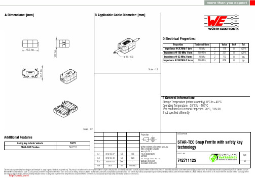
7.1 7.0 6.02012-06-272012-04-302008-01-03SStSStSMuSStSMu-Würth Elektronik eiSos GmbH & Co. KGEMC & Inductive SolutionsMax-Eyth-Str. 174638 WaldenburgGermanyTel. +49 (0) 79 42 945 - 0A Dimensions: [mm] Additional FeaturesSafety key to lock/ unkock STAR-CLIP Fixation74271 7427711D2 General Properties:Ferrite core Ferrite core Ferrite core Plastic housing Plastic housing Test cable Test cablePropertiesMaterial Initial permeability Curie temperatureColourFlammability ClassificationApplicable cable Applicable cable lengthµi T CValue 4 W 620620150Black UL94-V0AWG2690Unit°Cmm Tol.typ.typ.F Typical Impedance Characteristics:I Cautions and Warnings:The following conditions apply to all goods within the product series of WE-STAR TECof Würth Elektronik eiSos GmbH & Co. KG:General:All recommendations according to the general technical specifications of the data sheet have to be complied with.The disposal and operation of the product within ambient conditions which probably alloy or harm the component surface has to be avoided.The packaging of the product is to encase the needed humidity of the plastic housing. To ensure the humidity level, the products have to be stored in this delivered packaging. If not, the products are losing their humidity. In this case you can re-condition the components according to the internal standard WE1883 to ensure the necessary humidity in the plastic.To ensure the operating mode of the product, the ambient temperature at processing (when the part will be mounted on the cable) has to be in the range of 15 to 25 °C.Before mounting, the part should be stored for one hour in this condition.The responsibility for the applicability of customer specific products and the use in a particular customer design is always within the authority of the customer. All technical specifications for standard products do also apply for customer specific products.Direct mechanical impact to the product and the forcible closing of this shall be prevented as the ferrite material of the ferrite body or the pla-stic housing could flake or in the worst case it could break.Product specific:Follow all instructions mentioned in the datasheet, especially:•The cable diameter must be pointed out, otherwise no warranty will be sustained.•Violation of the technical product specifications such as exceeding the nominal rated current will result in the loss of warranty.1. General Customer ResponsibilitySome goods within the product range of Würth Elektronik eiSos GmbH & Co. KG contain statements regarding general suitability for certain application areas. These statements about suitability are based on our knowledge and experience of typical requirements concerning the are-as, serve as general guidance and cannot be estimated as binding statements about the suitability for a customer application. The responsibi-lity for the applicability and use in a particular customer design is always solely within the authority of the customer. Due to this fact it is up to the customer to evaluate, where appropriate to investigate and decide whether the device with the specific product characteristics described in the product specification is valid and suitable for the respective customer application or not.2. Customer Responsibility related to Specific, in particular Safety-Relevant ApplicationsIt has to be clearly pointed out that the possibility of a malfunction of electronic components or failure before the end of the usual lifetime can-not be completely eliminated in the current state of the art, even if the products are operated within the range of the specifications.In certain customer applications requiring a very high level of safety and especially in customer applications in which the malfunction or failure of an electronic component could endanger human life or health it must be ensured by most advanced technological aid of suitable design of the customer application that no injury or damage is caused to third parties in the event of malfunction or failure of an electronic component.3. Best Care and AttentionAny product-specific notes, warnings and cautions must be strictly observed.4. Customer Support for Product SpecificationsSome products within the product range may contain substances which are subject to restrictions in certain jurisdictions in order to serve spe-cific technical requirements. Necessary information is available on request. In this case the field sales engineer or the internal sales person in charge should be contacted who will be happy to support in this matter.5. Product R&DDue to constant product improvement product specifications may change from time to time. As a standard reporting procedure of the Product Change Notification (PCN) according to the JEDEC-Standard inform about minor and major changes. In case of further queries regarding the PCN, the field sales engineer or the internal sales person in charge should be contacted. The basic responsibility of the customer as per Secti-on 1 and 2 remains unaffected.6. Product Life CycleDue to technical progress and economical evaluation we also reserve the right to discontinue production and delivery of products. As a stan-dard reporting procedure of the Product Termination Notification (PTN) according to the JEDEC-Standard we will inform at an early stage about inevitable product discontinuance. According to this we cannot guarantee that all products within our product range will always be available. Therefore it needs to be verified with the field sales engineer or the internal sales person in charge about the current product availability ex-pectancy before or when the product for application design-in disposal is considered.The approach named above does not apply in the case of individual agreements deviating from the foregoing for customer-specific products.7. Property RightsAll the rights for contractual products produced by Würth Elektronik eiSos GmbH & Co. KG on the basis of ideas, development contracts as well as models or templates that are subject to copyright, patent or commercial protection supplied to the customer will remain with Würth Elektronik eiSos GmbH & Co. KG.8. General Terms and ConditionsUnless otherwise agreed in individual contracts, all orders are subject to the current version of the “General Terms and Conditions of Würth Elektronik eiSos Group”, last version available at .J Important Notes:The following conditions apply to all goods within the product range of Würth Elektronik eiSos GmbH & Co. KG:分销商库存信息: WURTH-ELECTRONICS 74271112S。
ATT7022中文资料
2、引脚描述 引脚 标识 1 RESET 2 SIG
3,4 6,7 9,10 5 11 13,14 16,17 19,20 24 26 27
V1P/V1N V3P/V3N V5P/V5N REFCAP REFOUT V2P/V2N V4P/V4N V6P/V6N TEST SEL CF1
28
CF2
35 36 37 38 40
RESET 1 SIG V1P V1N
2 3 4
33 VDD 32 NC 31 NC 30 NC
REFCAP 5 V3P 6 V3N AGND V5P
7 8 9
ATT7022
29 NC 28 CF2 27 CF1 26 SEL 25
NC
V5N 10 REFOUT 11
12 13 14 15 16 17 18 19 20 21 22
24 TEST 23 GND
A V C C
V V 2 2 P N
A V V G 4 4 N P N D
A V C C
V 6 P
V 6 N
N C
N C
第 5 页 共 32 页
珠海炬力集成电路设计有限公司
Actions Semiconductor Co., Ltd.
时间
复位
运行
复位
片内电源监控特性 §2.2 模数转换 ATT7022 片内集成了 6 路 16 位的 ADC,采用双端差分信号输入。最大输入电 压是 1.5v,即可以输入最大的正弦信号有效值是 1v。建议将电压通道 Un 对应到 ADC 的输入选在 0.5v 左右,而电流通道 Ib 时的 ADC 输入选在 0.1v 左右。 ADC 内部结构图:
第 3 页 共 32 页
AT91SAM7A3-AU;中文规格书,Datasheet资料
Features Array•Incorporates the ARM7TDMI ® ARM® Thumb® Processor–High-performance 32-bit RISC Architecture–High-density 16-bit Instruction Set–Leader in MIPS/Watt•EmbeddedICE™ In-circuit Emulation, Debug Communication Channel Support•256 Kbytes of Internal High-speed Flash, Organized in 1024 Pages of 256 Bytes –Single Cycle Access at Up to 30 MHz in Worst Case Conditions–Prefetch Buffer Optimizing Thumb Instruction Execution at Maximum Speed–Page Programming Time: 6 ms, Including Page Auto-erase, Full Erase Time: 15 ms –10,000 Write Cycles, 10-year Data Retention Capability, Sector Lock Capabilities •32K Bytes of Internal High-speed SRAM, Single-cycle Access at Maximum Speed •Memory Controller (MC)–Embedded Flash Controller, Abort Status and Misalignment Detection–Memory Protection Unit•Reset Controller (RSTC)–Based on Three Power-on Reset Cells–Provides External Reset Signal Shaping and Reset Sources Status•Clock Generator (CKGR)–Low-power RC Oscillator, 3 to 20 MHz On-chip Oscillator and One PLL•Power Management Controller (PMC)–Power Optimization Capabilities, including Slow Clock Mode (Down to 500 Hz), Idle Mode, Standby Mode and Backup Mode–Four Programmable External Clock Signals•Advanced Interrupt Controller (AIC)–Individually Maskable, Eight-level Priority, Vectored Interrupt Sources–Four External Interrupt Sources and One Fast Interrupt Source, Spurious Interrupt Protected•Debug Unit (DBGU)–2-wire UART and Support for Debug Communication Channel interrupt •Periodic Interval Timer (PIT)–20-bit Programmable Counter plus 12-bit Interval Counter•Windowed Watchdog (WDT)–12-bit key-protected Programmable Counter–Provides Reset or Interrupt Signal to the System–Counter May Be Stopped While the Processor is in Debug Mode or in Idle State •Real-time Timer (RTT)–32-bit Free-running Counter with Alarm–Runs Off the Internal RC Oscillator•Two Parallel Input/Output Controllers (PIO)–Sixty-two Programmable I/O Lines Multiplexed with up to Two Peripheral I/Os–Input Change Interrupt Capability on Each I/O Line–Individually Programmable Open-drain, Pull-up resistor and Synchronous Output •Shutdown Controller (SHDWC)–Programmable Shutdown Pin and Wake-up Circuitry•Two 32-bit Battery Backup Registers for a Total of 8 Bytes•One 8-channel 20-bit PWM Controller (PWMC)•One USB 2.0 Full Speed (12 Mbits per Second) Device Port–On-chip Transceiver, 2376-byte Configurable Integrated FIFOs26042DS–ATARM–14-Dec-06AT91SAM7A3•Nineteen Peripheral DMA Controller (PDC) Channels•Two CAN 2.0B Active Controllers, Supporting 11-bit Standard and 29-bit Extended Identifiers –16 Fully Programmable Message Object Mailboxes, 16-bit Time Stamp Counter •Two 8-channel 10-bit Analog-to-Digital Converter•Three Universal Synchronous/Asynchronous Receiver Transmitters (USART)–Individual Baud Rate Generator, IrDA ® Infrared Modulation/Demodulation–Support for ISO7816 T0/T1 Smart Card, Hardware Handshaking, RS485 Support •Two Master/Slave Serial Peripheral Interfaces (SPI)–8- to 16-bit Programmable Data Length, Four External Peripheral Chip Selects •Three 3-channel 16-bit Timer/Counters (TC)–Three External Clock Inputs, Two Multi-purpose I/O Pins per Channel –Double PWM Generation, Capture/Waveform Mode, Up/Down Capability •Two Synchronous Serial Controllers (SSC)–Independent Clock and Frame Sync Signals for Each Receiver and Transmitter –I²S Analog Interface Support, Time Division Multiplex Support–High-speed Continuous Data Stream Capabilities with 32-bit Data Transfer •One Two-wire Interface (TWI)–Master Mode Support Only, All Two-wire Atmel EEPROM’s Supported •Multimedia Card Interface (MCI)–Compliant with Multimedia Cards and SD Cards–Automatic Protocol Control and Fast Automatic Data Transfers with PDC, MMC and SDCard Compliant •IEEE ® 1149.1 JTAG Boundary Scan on All Digital Pins •Required Power Supplies–Embedded 1.8V Regulator, Drawing up to 130 mA for the Core and the External Components, Enables 3.3V Single Supply Mode–3.3V VDD3V3 Regulator, I/O Lines and Flash Power Supply–1.8V VDD1V8 Output of the Voltage Regulator and Core Power Supply –3V to 3.6V VDDANA ADC Power Supply –3V to 3.6V VDDBU Backup Power Supply •5V-tolerant I/Os•Fully Static Operation: Up to 60 MHz at 1.65V and 85°C Worst Case Conditions •Available in a 100-lead LQFP Green Package36042DS–ATARM–14-Dec-06AT91SAM7A31.DescriptionThe AT91SAM7A3 is a member of a series of 32-bit ARM7™ microcontrollers with an integrated CAN controller. It features a 256-Kbyte high-speed Flash and 32-Kbyte SRAM, a large set of peripherals, including two 2.0B full CAN controllers, and a complete set of system functions min-imizing the number of external components. The device is an ideal migration path for 8-bit microcontroller users looking for additional performance and extended memory.The embedded Flash memory can be programmed in-system via the JTAG-ICE interface. Built-in lock bits protect the firmware from accidental overwrite.The AT91SAM7A3 integrates a complete set of features facilitating debug, including a JTAG Embedded ICE interface, misalignment detector, interrupt driven debug communication channel for user configurable trace on a console, and JTAG boundary scan for board level debug and test.By combining a high-performance 32-bit RISC processor with a high-density 16-bit instruction set, Flash and SRAM memory, a wide range of peripherals including CAN controllers, 10-bit ADC, Timers and serial communication channels, on a monolithic chip, the AT91SAM7A3 is ideal for many compute-intensive embedded control applications.46042DS–ATARM–14-Dec-06AT91SAM7A32.Block DiagramFigure 2-1.AT91SAM7A3 Block Diagram56042DS–ATARM–14-Dec-06AT91SAM7A33.Signal DescriptionTable 3-1.Signal DescriptionSignal NameFunctionTypeActive LevelCommentsPowerVDD3V3 1.8V Voltage Regulator, I/O Lines and Flash Power SupplyPower 3.0V to 3.6V VDDBU Backup I/O Lines Power Supply Power 3V to 3.6V VDDANA Analog Power SupplyPower 3V to 3.6V VDD1V8 1.8V Voltage Regulator Output and Core Power SupplyPower 1.85V typical VDDPLL 1.8V PLL Power Supply Power 1.65V to 1.95VGNDGroundGroundClocks, Oscillators and PLLsXIN Main Oscillator Input Input XOUT Main Oscillator Output Output PLLRC PLL FilterInput PCK0 - PCK3Programmable Clock Output Output SHDWShut-Down Control Output Open Drain.WKUP0 - WKUP1Wake-Up Inputs Input Accept between 0V and VDDBU FWKUPForce Wake UpInputAccept between 0V and VDDBU External pull-up resistor needed.ICE and JTAGTCK T est Clock Input No pull-up resistor TDI T est Data In Input No pull-up resistorTDO T est Data Out Output TMS T est Mode Select Input No pull-up resistor JT AGSELJTAG SelectionInputPull-down resistor Reset/TestNRST Microcontroller Reset I/O Low TSTT est Mode SelectInputHighPull-down resistorDebug UnitDRXD Debug Receive Data Input DTXDDebug Transmit DataOutput66042DS–ATARM–14-Dec-06AT91SAM7A3AICIRQ0 - IRQ3External Interrupt Inputs Input FIQFast Interrupt InputInputPIOP A0 - P A31Parallel IO Controller A I/O Pulled-up input at reset PB0 - PB29Parallel IO Controller BI/OPulled-up input at resetMultimedia Card InterfaceMCCK Multimedia Card Clock Output MCCDAMultimedia Card A Command I/O MCDA0 - MCDA3Multimedia Card A DataI/OUSB Device PortDDM USB Device Port Data - Analog DDPUSB Device Port Data +Analog USARTSCK0 - SCK1 - SCK2Serial Clock I/O TXD0 - TXD1 - TXD2T ransmit Data I/O RXD0 - RXD1 - RXD2Receive Data Input RTS0 - RTS1 - RTS2Request To Send Output CTS0 - CTS1 - CTS2Clear To SendInputSynchronous Serial ControllerTD0 - TD1T ransmit Data Output RD0 - RD1Receive Data Input TK0 - TK1T ransmit Clock I/O RK0 - RK1Receive Clock I/O TF0 - TF1T ransmit Frame Sync I/O RF0 - RF1Receive Frame SyncI/O Timer/CounterTCLK0 - TCLK8External Clock Input Input TIOA0 - TIOA8I/O Line A I/O TIOB0 - TIOB8I/O Line BI/O PWM ControllerPWM0 - PWM7PWM ChannelsOutput Table 3-1.Signal Description (Continued)Signal NameFunctionTypeActive LevelComments76042DS–ATARM–14-Dec-06AT91SAM7A3SPISPI0_MISO SPI1_MISO Master In Slave Out I/O SPI0_MOSI SPI1_MOSI Master Out Slave In I/O SPI0_SPCK SPI1_SPCK SPI Serial ClockI/O SPI0_NPCS0SPI1_NPCS0SPI Peripheral Chip Select 0I/O Low SPI0_NPCS1 - SPI0_NPCS3SPI1_NPCS1 - SPI1_NPCS3SPI Peripheral Chip SelectOutputLowTwo-wire InterfaceTWD T wo-wire Serial Data I/O TWCKT wo-wire Serial ClockI/OAnalog-to-Digital ConverterADC0_AD0 - ADC0_AD7ADC1_AD0 - ADC1_AD7Analog InputsAnalog Digital pulled-up inputs at resetADVREFP Analog Positive Reference Analog ADC0_ADTRG ADC1_ADTRGADC TriggerInputCAN ControllerCANRX0-CANRX1CAN Inputs Input CANTX0-CANTX1CAN OutputsOutput Table 3-1.Signal Description (Continued)Signal NameFunctionTypeActive LevelComments86042DS–ATARM–14-Dec-06AT91SAM7A34.Package4.1100-lead LQFP Package OutlineFigure 4-1shows the orientation of the 100-lead LQFP package. A detailed mechanical descrip-tion is given in the Mechanical Characteristics section of the full datasheet.Figure 4-1.100-lead LQFP Outline (Top View)96042DS–ATARM–14-Dec-06AT91SAM7A34.2PinoutTable 4-1.Pinout in 100-lead LQFP Package1GND 26VDDBU 51P A2076PLLRC 2NRST 27FWKUP 52P A2177VDDANA 3TST 28WKUP053P A2278ADVREFP 4PB1329WKUP154P A2379GND 5PB1230SHDW 55P A2480PB14/ADC0_AD06PB1131GND 56P A2581PB15/ADC0_AD17PB1032P A457P A2682PB16/ADC0_AD28PB933P A558P A2783PB17/ADC0_AD39PB834P A659VDD1V884PB18/ADC0_AD410PB735P A760GND 85PB19/ADC0_AD511PB636P A861VDD3V386PB20/ADC0_AD612PB537P A962P A2887PB21/ADC0_AD713PB438VDD3V363P A2988VDD3V314PB339GND 64P A3089PB22/ADC1_AD015VDD3V340VDD1V865P A3190PB23/ADC1_AD116GND 41P A1066JTAGSEL 91PB24/ADC1_AD217VDD1V842P A1167TDI 92PB25/ADC1_AD318PB243P A1268TMS 93PB26/ADC1_AD419PB144P A1369TCK 94PB27/ADC1_AD520PB045P A1470TDO 95PB28/ADC1_AD621P A046P A1571GND 96PB29/ADC1_AD722P A147P A1672VDDPLL 97DDM 23P A248P A1773XOUT 98DDP 24P A349P A1874XIN 99VDD1V825GND50P A1975GND100VDD3V3106042DS–ATARM–14-Dec-06AT91SAM7A35.Power Considerations5.1Power SuppliesThe AT91SAM7A3 has five types of power supply pins:•VDD3V3 pins. They power the voltage regulator, the I/O lines, the Flash and the USB transceivers; voltage ranges from 3.0V to 3.6V , 3.3V nominal.•VDD1V8 pins. They are the outputs of the 1.8V voltage regulator and they power the logic of the device.•VDDPLL pin. It powers the PLL; voltage ranges from 1.65V to 1.95V , 1.8V typical. They can be connected to the VDD1V8 pin with decoupling capacitor.•VDDBU pin. It powers the Slow Clock oscillator and the Real Time Clock, as well as a part of the System Controller; ranges from 3.0V and 3.6V , 3.3V nominal.•VDDANA pin. It powers the ADC; ranges from 3.0V and 3.6V , 3.3V nominal.No separate ground pins are provided for the different power supplies. Only GND pins are pro-vided and should be connected as shortly as possible to the system ground plane.5.2Voltage RegulatorThe AT91SAM7A3 embeds a voltage regulator that consumes less than 120 µA static current and draws up to 130 mA of output current.Adequate output supply decoupling is mandatory for VDD1V8 (pin 99)to reduce ripple and avoid oscillations. The best way to achieve this is to use two capacitors in parallel: one external 470 pF (or 1 nF) NPO capacitor must be connected between VDD1V8 and GND as close to the chip as possible. One external 3.3 µF (or 4.7 µF) X7R capacitor must be connected between VDD1V8and GND.All other VDD1V8 pins must be externally connected and have a proper decoupling capacitor (at least 100 nF).Adequate input supply decoupling is mandatory for VDD3V3 (pin 100) in order to improve star-tup stability and reduce source voltage drop. The input decoupling capacitor should be placed close to the chip. For example, two capacitors can be used in parallel: 100 nF NPO and 4.7 µF X7R.All other VDD3V3 pins must be externally connected and have a proper decoupling capacitor (at least 100 nF).分销商库存信息: ATMELAT91SAM7A3-AU。
RC7222-A2

V1.1
2005-09-20
V1.20
2005-12-22
V1.21
2007-09-19
注意:V2.00 以上版本适用于 RC7222-A1 芯片 V2.00 V2.01 V2.02 2009-06-01 2009-06-18 EL: +86-10-80106100
RC7222-A2 用户手册 V2.11
Page 3
3.修改通过 I2C 接口访问 PHY 的指令 2 芯片 注意:V2.10 以上版本适用于 RC7222-A RC7222-A2 V2.10 V2.11 2010-07-01 2010-07-20 1.增加 SSI 接口描述; 2.增加 GFP 封装描述; 1. 章节整理,文字错误整理;
Page 2
版本记录
版本编号 V1.0 日期 2005-01-30 更改说明 文档创建。本文档适用于 RC7222 1、原文档的 23 页,删除表 3.2.2。 2、原文档中管脚 119,名称由 STBUS_PLUSO,改为 STBUS_PULSEO。 3、原文档的37页,4.6.3节中“和网管寄存器04H 的bit1-0 bit3-1”。 4、 原文档的 37 页“建议 ADDR_FILTI 与以太网 PHY 芯片的全 /半双工指示管脚连接”描述不全面,改为“建议使用 PHY 芯片输 出的固定电平的信号(半双工指示或 10M 速率指示)连接 RC7222 的 ADDR_FILTI 管脚”。 5、 原文档 46 页, 4.13.1 节修改对 TEST3_LEDO、 TEST4_LEDO 的功能描述。 6、原文档 49 页,表 5.1.2.3,对指令类型的描述“00H02H:查 询 RC7222”。 7、原文档 49 页,表 5.1.2.3,对配置数据的描述“如果配置 RC7222 内部寄存器,只有字节 98 有效;配置 PHY 的 MDIO 寄存器,字节 9、118、10 有效,其中 9 8 为高字节”。 8、原文档表5.4.1中04H的bit2,将名称MAC_FULL改为 DUPLEX_MOD。 9、原文档60页,表5.4.6对53H-56H的带宽对应顺序描述颠倒 了,“对07H 至0AH 的配置,53H 对应07H,56H 对应0AH” 改为“对0AH至07H的配置,53H对应0AH,56H对应07H”。 10、增加了与 SDRAM 兼容型号的提示。 1、 网管寄存器 06H 改为不允许被配置。 要求不写入 52H 和 59H。 2、 更改了 Uart 查询和设置指令帧格式, 将表 5.1.2.1 和表 5.1.2.3 中 REGAddr 的排列顺序进行了颠倒。 3、更改 P121 UART_DO/SDA 管脚属性,该管脚不是三态。 4、将表 5.4.1 中“从 REG07 最高比特 7 至 REG10 最低比特 0” 的描述改称为“从 07H 最高比特 7 至 0AH 最低比特 0”。 5、将 State_Alarm0、State_Alarm1、State_Alarm2、 State_Alarm3 命名改为 Status_Alarm0、Status_Alarm1、 Status_Alarm2、Status_Alarm3。 6、在 4.5.1 节增加了对 sdram 型号支持的说明。 1.更新管脚排列图 2.修改 5.6 章节和 5.7 章节的内容 文档创建。本文档适用于 RC7222-A1 增加 RJ017 帧格式描述 1.修改书签显示错误; 2.将各图中环回方向进行精确描述
2N7002-7-F;2N7002-7;中文规格书,Datasheet资料
Marking Information
Date Code Key
Year
2002
Code
NБайду номын сангаас
C72
Chengdu A/T Site
YM YM
K72
Shanghai A/T Site
K = SAT (Shanghai Assembly/ Test site) C = CAT (Chengdu Assembly/ Test site) 72= Product Type Marking Code YM = Date Code Marking Y = Year (ex: N = 2002) M = Month (ex: 9 = September)
Applications
• Motor control • Power Management Functions
Mechanical Data
• Case: SOT23 • Case Material: Molded Plastic, “Green” Molding Compound.
UL Flammability Classification Rating 94V-0 • Moisture Sensitivity: Level 1 per J-STD-020 • Terminals: Matte Tin Finish annealed over Alloy 42 leadframe
Code V12 are built with Non-Green Molding Compound and may contain Halogens or Sb2O3 Fire Retardants. 5. For packaging details, go to our website at .
FDS8949;中文规格书,Datasheet资料

tmOctober 2006FDS8949 Dual N-Channel Logic Level PowerTrench®MOSFET FDS8949Dual N-Channel Logic Level PowerTrench® MOSFET40V, 6A, 29mΩFeaturesMax r DS(on)= 29mΩ at V GS = 10VMax r DS(on)= 36mΩ at V GS = 4.5VLow gate chargeHigh performance trench technology for extremely lowr DS(on)High power and current handling capabilityRoHS compliantGeneral DescriptionThese N-Channel Logic Level MOSFETs are producedusing Fairchild Semiconductor’s advancedPowerTrench® process that has been especially tailoredto minimize the on-state resistance and yet maintainsuperior switching performance.These devices are well suited for low voltage andbattery powered applications where low in-line powerloss and fast switching are required.ApplicationsInverterPower suppliersMOSFET Maximum Ratings TA = 25°C unless otherwise notedThermal CharacteristicsPackage Marking and Ordering InformationSymbol Parameter Ratings UnitsV DS Drain to Source Voltage40VV GS Gate to Source Voltage±20VI DDrain Current -Continuous (Note 1a)6A -Pulsed 20E AS Drain-Source Avalanche Energy (Note 3)26mJP DPower Dissipation for Dual Operation 2W Power Dissipation for Single Operation (Note 1a)(Note 1b)1.60.9T J, T STG Operating and Storage Junction Temperature Range-55 to 150°CRθJA Thermal Resistance-Single operation, Junction to Ambient (Note 1a)81°C/WRθJA Thermal Resistance-Single operation, Junction to Ambient (Note 1b)135RθJC Thermal Resistance, Junction to Case (Note 1)40Device Marking Device Reel Size Tape Width Quantity FDS8949FDS894913’’12mm2500 unitsPin 1SO-8D1D1D2D2S2S1G1G2FDS8949 Dual N-Channel Logic Level PowerTrench ® MOSFETElectrical Characteristics TJ = 25°C unless otherwise notedSymbolParameterTest ConditionsMinTypMaxUnitsOff Characteristics BV DSS Drain to Source Breakdown Voltage I D = 250µA, V GS = 0V 40 V ∆BV DSS ∆T J Breakdown Voltage Temperature CoefficientI D = 250µA, referenced to 25°C33mV/°C I DSS Zero Gate Voltage Drain Current V DS = 32V, V GS = 0V1µA T J = 55°C10µA I GSSGate to Source Leakage CurrentV GS = ±20V,V DS = 0V±100nAOn Characteristics V GS(th)Gate to Source Threshold Voltage V GS = V DS , I D = 250µA 1 1.93V ∆V GS(th) ∆T J Gate to Source Threshold Voltage Temperature Coefficient I D = 250µA, referenced to 25°C -4.6 mV/°Cr DS(on)Drain to Source On Resistance V GS = 10V, I D = 6A2129m ΩV GS = 4.5V, I D = 4.5A 2636V GS = 10V, I D = 6A,T J = 125°C 2943g FSForward TransconductanceV DS = 10V,I D = 6A22S (Note 2)Dynamic CharacteristicsC iss Input Capacitance V DS = 20V, V GS = 0V,f = 1MHz 715955pF C oss Output Capacitance105140pF C rss Reverse Transfer Capacitance6090pF R gGate Resistancef = 1MHz1.1ΩSwitching Characteristicst d(on)Turn-On Delay Time V DD = 20V, I D = 1A V GS = 10V, R GEN = 6Ω918ns t r Rise Time510ns t d(off)Turn-Off Delay Time 2337ns t f Fall Time36ns Q g Total Gate ChargeV DS = 20V, I D = 6A,V GS = 5V 7.711nC Q gs Gate to Source Gate Charge 2.4nC Q gdGate to Drain “Miller”Charge2.8nCDrain-Source Diode Characteristics V SD Source to Drain Diode Forward Voltage V GS = 0V, I S = 6A (note 2) 0.8 1.2V t rr Reverse Recovery Time (note 3)I F = 6A, d iF /d t = 100A/µs1726ns Q rrReverse Recovery Charge711nCand Maximum RatingsNotes:1: R θJA is the sum of the junction-to-case and case-to- ambient thermal resistance where the case thermal reference is defined as the solder mounting surface of the drain pins. R θJC is guaranteed by design while R θJA is determined by the user’s board design.2: Pulse Test: Pulse Width < 300 us, Duty Cycle < 2.0%.3: Starting T J = 25°C, L = 1mH, I AS = 7.3A, V DD = 40V, V GS = 10V.Scale 1:1 on letter size papera) 81°C/W when mounted on a 1in 2 pad of 2 oz copperb) 135°C/W when mounted on a minimum pad .MOSFETMOSFETMOSFETFDS8949 Rev. 6FDS8949 Dual N-Channel Logic Level PowerTrench ® MOSFETTRADEMARKSThe following are registered and unregistered trademarks Fairchild Semiconductor owns or is authorized to use and is not intended to be an exhaustive list of all such trademarks.DISCLAIMERFAIRCHILD SEMICONDUCTOR RESERVES THE RIGHT TO MAKE CHANGES WITHOUT FURTHER NOTICE TO ANY PRODUCTS HEREIN TO IMPROVE RELIABILITY, FUNCTION OR DESIGN. FAIRCHILD DOES NOT ASSUME ANY LIABILITY ARISING OUT OF THE APPLICATION OR USE OF ANY PRODUCT OR CIRCUIT DESCRIBED HEREIN; NEITHER DOES IT CONVEY ANY LICENSE UNDER ITS PATENT RIGHTS, NOR THE RIGHTS OF OTHERS. THESE SPECIFICATIONS DO NOT EXPAND THE TERMS OF FAIRCHILD’S WORLDWIDE TERMS AND CONDITIONS, SPECIFICALLY THE WARRANTY THEREIN, WHICH COVERS THESE PRODUCTS.LIFE SUPPORT POLICYFAIRCHILD’S PRODUCTS ARE NOT AUTHORIZED FOR USE AS CRITICAL COMPONENTS IN LIFE SUPPORT DEVICES OR SYSTEMS WITHOUT THE EXPRESS WRITTEN APPROVAL OF FAIRCHILD SEMICONDUCTOR CORPORATION.As used herein:1. Life support devices or systems are devices or systems which, (a) are intended for surgical implant into the body, or (b) support or sustain life, or (c) whose failure to perform when properly used in accordance with instructions for use provided in the labeling, can be reasonably expected to result in significant injury to the user.2. A critical component is any component of a life support device or system whose failure to perform can be reasonably expected to cause the failure of the life support device or system, or to affect its safety or effectiveness.PRODUCT STATUS DEFINITIONS Definition of TermsACEx™ActiveArray™Bottomless™Build it Now™CoolFET™CROSSVOLT ™DOME™EcoSPARK™E 2CMOS™EnSigna™FACT™FAST ®FASTr™FPS™FRFET™FACT Quiet Series™ GlobalOptoisolator™GTO™HiSeC™I 2C™i-Lo ™ImpliedDisconnect ™IntelliMAX™ISOPLANAR™LittleFET™MICROCOUPLER™MicroFET™MicroPak™MICROWIRE™MSX ™MSXPro ™OCX ™OCXPro ™OPTOLOGIC ®OPTOPLANAR™PACMAN™POP™Power247™PowerEdge™PowerSaver™PowerTrench ®QFET ®QS™QT Optoelectronics™Quiet Series™RapidConfigure ™RapidConnect ™µSerDes ™ScalarPump ™SILENT SWITCHER ®SMART START™SPM™Stealth™SuperFET™SuperSOT™-3SuperSOT™-6SuperSOT™-8SyncFET™TCM™TinyBoost™TinyBuck™TinyPWM™TinyPower™TinyLogic ®TINYOPTO™TruTranslation™UHC™UniFET™UltraFET ®VCX™Wire™Across the board. Around the world.™The Power Franchise ®Programmable Active Droop™Datasheet Identification Product Status DefinitionAdvance InformationFormative or In Design This datasheet contains the design specifications for product development. Specifications may change in any manner without notice.PreliminaryFirst ProductionThis datasheet contains preliminary data, andsupplementary data will be published at a later date.Fairchild Semiconductor reserves the right to make changes at any time without notice in order to improve design.No Identification Needed Full ProductionThis datasheet contains final specifications. Fairchild Semiconductor reserves the right to make changes at any time without notice in order to improve design. Obsolete Not In ProductionThis datasheet contains specifications on a product that has been discontinued by Fairchild semiconductor.The datasheet is printed for reference information only.Rev. I20分销商库存信息: FAIRCHILDFDS8949。
AUIPS7221RTRL;AUIPS7221RTRR;AUIPS7221RTR;AUIPS7221R;中文规格书,Datasheet资料
Symbol
Vout Voffset Vin Vcc max. I in max. Pd Tj max.
Parameter
Maximum output voltage Maximum logic ground to load ground offset Maximum input voltage Maximum Vcc voltage Maximum input current Maximum power dissipation (internally limited by thermal protection) Rth=50°C/W 1”sqrt. footprint Max. storage & operating temperature junction temperature
Parameter
ON state resistance Tj=25°C ON state resistance Tj=150°C Operating voltage range with short circuit protection Supply current when Sleep mode Output leakage current Supply current when On Output current when Off Input high threshold voltage Input low threshold voltage Input hysteresis Input current when the part is on Input voltage when the part is in fault mode
July, 2nd 2010
Automotive grade
MAC722 PAC722 中文产品说明书

I N S T A L L A T I O N I N S T R U C T I O N SMedium/Large Side-by-Side Accessoryfor Carts and StandsDutch Product DescriptionMAC722 / PAC722MAC722 / PAC722Installation Instructions2DISCLAIMERMilestone AV Technologies and its affiliated corporations and subsidiaries (collectively "Milestone"), intend to make thismanual accurate and complete. However, Milestone makes no claim that the information contained herein covers all details,conditions or variations, nor does it provide for every possible contingency in connection with the installation or use of this product. The information contained in this document is subject to change without notice or obligation of any kind. Milestone makes no representation of warranty, expressed or implied,regarding the information contained herein. Milestone assumes no responsibility for accuracy, completeness or sufficiency of the information contained in this document.Chief® is a registered trademark of Milestone AV Technologies.All rights reserved.IMPORTANT WARNINGS AND CAUTIONS!WARNING: A WARNING alerts you to the possibility ofserious injury or death if you do not follow the instructions.CAUTION: A CAUTION alerts you to the possibility ofdamage or destruction of equipment if you do not follow the corresponding instructions.WARNING:Failure to read, thoroughly understand, andfollow all instructions can result in serious personal injury,damage to equipment, or voiding of factory warranty! It is the installer’s responsibility to make sure all components are properly assembled and installed using the instructions provided.WARNING:Failure to provide adequate structural strengthfor this component can result in serious personal injury or damage to equipment! It is the installer’s responsibility to make sure the structure to which this component is attached can support five times the combined weight of all equipment.Reinforce the structure as required before installing the component. The wall to which the mount is being attached may have a maximum drywall thickness of 5/8" (1.6cm).WARNING:Exceeding the weight capacity can result inserious personal injury or damage to equipment! It is the installer’s responsibility to make sure the combined weight of all components located on the accessory does not exceed 150 lbs (68.0 kg) [75 lbs (34.0) per faceplate].LEGENDApretar elemento de fijación Befestigungsteil festziehen Apertar fixador Serrare il fissaggio Bevestiging vastdraaien Serrez les fixations Aflojar elemento de fijación Befestigungsteil lösen Desapertar fixador Allentare il fissaggio Bevestiging losdraaien Desserrez les fixationsLlave de cabeza hexagonal Sechskantschlüssel Chave de cabeça sextavada Chiave esagonale Zeskantsleutel Clé à tête hexagonale Llave de boca Gabelschlüssel Chave de bocas Chiave a punte aperte Steeksleutel Clé à fourcheInstallation Instructions MAC722 / PAC722 DIMENSIONS3MAC722 / PAC722Installation Instructions TOOLS REQUIRED FOR INSTALLATIONPARTS4Installation Instructions MAC722 / PAC722Assembly and InstallationThe MAC722 and PAC722 side-by-side accessories are for usewith Chief carts and stands.3.Attach faceplates (B and C)OR(D and E) to the extensionassembly (A) using two 5/16-18 x 3-1/2" button head capscrews (F) and two 5/16" locking nuts (G) for eachfaceplate. (See Figure 3)6WARNING:CART/STAND OR DISPLAY FALLING CAUSING SERIOUS PERSONAL INJURY OR DAMAGE TO EQUIPMENT!Extension measurement MUST be the same for both sides of the MAC722/PAC722.Attaching DisplaysWARNING:MAY LEAD TO SERIOUS PERSONAL INJURY ORDAMAGE TO EQUIPMENT! It is the installer’s responsibility to ensure the total amount of weight placed on the MAC722/PAC722 does not exceed 150 lbs (68.0 kg) [75 lbs (34.0) per faceplate].WARNING:PAC722 ensure the stand or cart is on a level surface.CAUTION:MAC722/PAC722 is evenly distributed.CAUTION:adjusting the height of the stand or cart.1.Adjust the stand or cart to the desired height by slightly lifting the inner column, pulling out knob on the center post and turning 90mechanism. (See Figure 6)2.Raise or lower the center post, then turn the knob 90direction to engage the knob and lock the stand at desired height. (See Figure 6)3.Attach interface brackets to the displays following the instructions included with the bracket.4.While supporting both sides of display, align four mounting buttons on display or interface bracket with four mounting holes in head assembly. (See Figures 10 and 11)(PAC722 shown)Two holes for full extensionInner ColumnWARNING:40 LBS! Always use two people and proper lifting techniques when installing or positioning display on stand.5.Lower display into place listening for audible "click" toensure recessed area of mounting buttons are properlyseated in lower area of mounting holes.(See Figure 7) and (See Figure 8)WARNING:STAND OR DISPLAY FALLING CAUSING SERIOUS PERSONAL INJURY OR DAMAGE TO EQUIPMENT! Ensure mounting buttons are completely engaged in mounting holes.NOTE:the pin and nut may be removed from the upper holesand moved to the lower holes for use as a morepermanent locking device. (See Figure 8)Figure 8Tilting DisplayThe display(s) can be tilted up to 5o either backward or forward from a straight upright position.1.Turn knob counterclockwise on back of faceplate to loosenthe tilt. (See Figure 9)Figure 92.Tilt display as desired, to a maximum of 5o either forward orbackward.3.Turn knob clockwise to tighten display on head assembly.(See Figure 9)CAUTION:Tighten knob on back of faceplate to prevent damage to the stand or cart.4.If leaving the display in a straight upright position, it isrecommended that a bolt (not provided) be placed through the faceplate (See Figure 9) to lock the display into theupright position.5.Repeat Steps 1-4 for remaining faceplate and display. Cable Management1.The display power cords can be run through the front of theextension assembly (A). (See Figure 4)2.The cords can then run through the extension assembly tothe center of the assembly. (See Figure 4)3.When the cords are run to the center of the extensionassembly, they can either exit out the front, or down through the cart or stand column. (See Figure 4)4.Any accessory power cords can be run through the frontFigure 10Remove pinand nut andmove to lower holes7MAC722 / PAC722Installation InstructionsUSA/InternationalA 8401 Eagle Creek Parkway, Savage, MN 55378P 800.582.6480 / 952.894.6280F 877.894.6918 / 952.894.6918EuropeA Fellenoord 130 5611 ZB EINDHOVEN, The Netherlands P +31 (0)40 2668620F +31 (0)40 2668615Asia PacificARoom 24F, Block D, Lily YinDu International BuildingLuoGang, BuJi Town, Shenzhen, CHINA.P +86-755-8996 9226F +86-755-8996 9217Chief Manufacturing, a products division of Milestone AV Technologies 8807-002006 Rev002009 Milestone AV Technologies, a Duchossois Group Company 06/09。
721分光光度计
6.1.2 开罩检视 ······································································································ 10
6.1.3 更换光源········································································································ 10
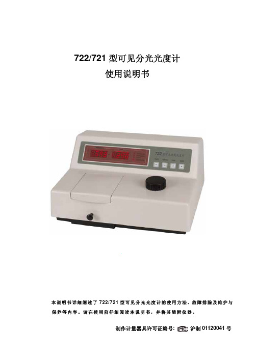
722/721 型可见分光光度计 使用说明书
本 说 明 书 详 细 阐 述 了 722/721 型 可 见 分 光 光 度 计 的 使 用 方 法 、故 障 排 除 及 维 护 与 保养等内容。请在使用前仔细阅读本说明书,并将其随附仪器。
制作计量器具许可证编号:
沪制 01120041 号
722 / 721 型可见分光光度计
7
5.2.4 运用 A-C(吸光度-浓度)标准曲线测定物质浓度················································
8
5.2.5 浓度直读应用··································································································
6
5.1.8 浓度因子设定和浓度直读设定········································································
6
5.1.9 RS232C 串行接口交换数据···········································································
IRMCK311TR;中文规格书,Datasheet资料
Data Sheet No. PD60338IRMCK311 Dual Channel Sensorless Motor Control IC forAppliancesFeaturesMCE TM (Motion Control Engine) - Hardware based computation engine for high efficiency sinusoidal sensorless control of permanent magnet AC motor Integrated Power Factor Correction controlSupports both interior and surface permanent magnet motorsBuilt-in hardware peripheral for single shunt current feedback reconstructionNo external current or voltage sensing operational amplifier requiredDual channel three/two-phase Space Vector PWM Three-channel analog output (PWM)Embedded 8-bit high speed microcontroller (8051) for flexible I/O and man-machine controlJTAG programming port for emulation/debugger Two serial communication interface (UART)I2C/SPI serial interfaceWatchdog timer with independent analog clockThree general purpose timers/countersTwo special timers: periodic timer, capture timer Internal ‘One-Time Programmable’ (OTP) memory and internal RAM for final production usagePin compatible with IRMCF311 RAM version1.8V/3.3V CMOS Product SummaryMaximum crystal frequency 60 MHz Maximum internal clock (SYSCLK) frequency 128 MHz Maximum 8051 clock frequency 33 MHz Sensorless control computation time 11 μsec typ MCE TM computation data range 16 bit signed 8051 OTP Program memory 56K bytes MCE program and Data RAM 8K bytes GateKill latency (digital filtered) 2 μsec PWM carrier frequency counter 16 bits/ SYSCLK A/D input channels 6 A/D converter resolution 12 bits A/D converter conversion speed 2 μsec 8051 instruction execution speed 2 SYSCLK Analog output (PWM) resolution 8 bits UART baud rate (typ) 57.6K bps Number of I/O (max) 14 Package (lead-free) QFP64 Operating temperature -40°C ~ 85°CDescriptionIRMCK311 is a high performance OTP based motion control IC designed primarily for appliance applications. IRMCK311 is designed to achieve low cost and high performance control solutions for advanced inverterized appliance motor control. IRMCK311 contains two computation engines. One is Motion Control Engine (MCE TM) for sensorless control of permanent magnet motors; the other is an 8-bit high-speed microcontroller (8051). Both computation engines are integrated into one monolithic chip. The MCE TM contains a collection of control elements such as Proportional plus Integral, Vector rotator, Angle estimator, Multiply/Divide, Low loss SVPWM, Single Shunt IFB. The user can program a motion control algorithm by connecting these control elements using a graphic compiler. Key components of the sensorless control algorithms, such as the Angle Estimator, are provided as complete pre-defined control blocks implemented in hardware. A unique analog/digital circuit and algorithm to fully support single shunt current reconstruction is also provided. The 8051 microcontroller performs 2-cycle instruction execution (16MIPS at 33MHz). The MCE and 8051 microcontroller are connected via dual port RAM to process signal monitoring and command input. An advanced graphic compiler for the MCE TM is seamlessly integrated into the MATLAB/Simulink environment, while third party JTAG based emulator tools are supported for 8051 developments. IRMCK311 comes with a small QFP64 pin lead-free package.TABLE OF CONTENTS1 Overview (5)2 IRMCK311 Block Diagram and Main Functions (6)3 Pinout (8)4 Input/Output of IRMCK311 (9)4.1 8051 Peripheral Interface Group (10)4.2 Motion Peripheral Interface Group (10)4.3 Analog Interface Group (11)4.4 Power Interface Group (11)4.5 Test Interface (12)5 Application Connections (13)6 DC Characteristics (14)6.1 Absolute Maximum Ratings (14)6.2 System Clock Frequency and Power Consumption (14)6.3 Digital I/O DC Characteristics (15)6.4 PLL and Oscillator DC Characteristics (15)6.5 Analog I/O DC Characteristics (16)6.6 Under Voltage Lockout DC Characteristics (17)6.7 AREF Characteristics (17)7 AC Characteristics (18)7.1 PLL AC Characteristics (18)7.2 Analog to Digital Converter AC Characteristics (19)7.3 Op Amp AC Characteristics (19)7.4 SYNC to SVPWM and A/D Conversion AC Timing (20)7.5 GATEKILL to SVPWM AC Timing (21)7.6 Interrupt AC Timing (21)7.7 I2C AC Timing (22)7.8 SPI AC Timing (23)7.8.1 SPI Write AC timing (23)7.8.2 SPI Read AC Timing (24)7.9 UART AC Timing (25)7.10 CAPTURE Input AC Timing (26)7.11 JTAG AC Timing (27)7.12 OTP Programming Timing (28)8 I/O Structure (29)9 Pin List (32)Dimensions (35)10 Package11 Part Marking Information (36)Information (36)12 OrderingTABLE OF FIGURESFigure 1. Typical Application Block Diagram Using IRMCK311 (5)Figure 2. IRMCK311 Internal Block Diagram (6)Figure 3. IRMCK311 Pin Configuration (8)Figure 4. Input/Output of IRMCK311 (9)Figure 5. Application Connection of IRMCK311 (13)Figure 6. Clock Frequency vs. Power Consumption (14)Figure 7 Crystal oscillator circuit (18)Figure 8 Voltage droop of sample and hold (19)Figure 9 SYNC to SVPWM and A/D conversion AC Timing (20)Figure 10 GATEKILL to SVPWM AC Timing (21)Figure 11 Interrupt AC Timing (21)Figure 12 I2C AC Timing (22)Figure 13 SPI AC Timing (23)Figure 14 SPI Read AC Timing (24)Figure 15 UART AC Timing (25)Figure 16 CAPTURE Input AC Timing (26)Figure 17 JTAG AC Timing (27)Figure 18 OTP Programming Timing (28)Figure 19 All digital I/O except motor PWM output (29)Figure 20 RESET, GATEKILL I/O (29)Figure 21 Analog input (30)Figure 22 Analog operational amplifier output and AREF I/O structure (30)Figure 23 VPP programming pin I/O structure (30)Figure 24 VSS and AVSS pin structure (31)Figure 25 VDD1 and VDDCAP pin structure (31)Figure 26 XTAL0/XTAL1 pins structure (31)TABLE OF TABLESTable 1. Absolute Maximum Ratings (14)Table 2. System Clock Frequency (14)Table 3. Digital I/O DC Characteristics (15)Table 4. PLL DC Characteristics (15)Table 5. Analog I/O DC Characteristics (16)Table 6. UVcc DC Characteristics (17)Table 7. AREF DC Characteristics (17)Table 8. PLL AC Characteristics (18)Table 9. A/D Converter AC Characteristics (19)Table 10. Current Sensing OP Amp AC Characteristics (19)Table 11. SYNC AC Characteristics (20)Table 12. GATEKILL to SVPWM AC Timing (21)Table 13. Interrupt AC Timing (21)Table 14. I2C AC Timing (22)Table 15. SPI Write AC Timing (23)Table 16. SPI Read AC Timing (24)Table 17. UART AC Timing (25)Table 18. CAPTURE AC Timing (26)Table 19. JTAG AC Timing (27)Table 20. OTP Programming Timing (28)Table 21. Pin List (32)1 OverviewIRMCK311 is a new International Rectifier integrated circuit device primarily designed as a one-chip solution for complete inverter controlled appliance dual motor control applications. Unlike a traditional microcontroller or DSP, the IRMCK311 provides a built-in closed loop sensorless control algorithm using the unique Motion Control Engine (MCE TM) for permanent magnet motors. The MCE TM consists of a collection of control elements, motion peripherals, a dedicated motion control sequencer and dual port RAM to map internal signal nodes. IRMCK311 also employs a unique single shunt current reconstruction circuit to eliminate additional analog/digital circuitry and enables a direct shunt resistor interface to the IC. The sensorless control is the same for both motors with a single shunt current sensing capability. Motion control programming is achieved using a dedicated graphical compiler integrated into the MATLAB/Simulink TM development environment. Sequencing, user interface, host communication, and upper layer control tasks can be implemented in the 8051 high-speed 8-bit microcontroller. The 8051 microcontroller is equipped with a JTAG port to facilitate emulation and debugging tools. Figure 1 shows a typical application schematic using IRMCK311.IRMCK311 is intended for volume production purpose and contains 64K bytes of OTP (One Time Programming) ROM, which can be programmed through a JTAG port. For a development purpose use, IRMCF311 contains a 48k byte of RAM in place of program OTP to facilitate an application development work. Both IRMCF311 and IRMCK311 come in the same 64-pin QFP package with identical pin configuration to facilitate PC board layout and transition to mass productionFigure 1. Typical Application Block Diagram Using IRMCK3112 IRMCK311 Block Diagram and Main FunctionsM o t i o n C o n t r o l B u sFigure 2. IRMCK311 Internal Block DiagramIRMCK311 contains the following functions for sensorless AC motor control applications:• Motion Control Engine (MCE TM )o Proportional plus Integral block o Low pass filtero Differentiator and lag (high pass filter) o Ramp o Limito Angle estimate (sensorless control) o Inverse Clark transformation o Vector rotator o Bit latch o Peak detect o Transitiono Multiply-divide (signed and unsigned)o Divide (signed and unsigned)o Addero Subtractoro Comparatoro Countero Accumulatoro Switcho Shifto ATAN (arc tangent)o Function block (any curve fitting, nonlinear function)o16-bit wide Logic operations (AND, OR, XOR, NOT, NEGATE)o MCE TM program and data memory (6K byte). Note 1o MCE TM control sequencer• 8051 microcontrollero Three 16-bit timer/counterso16-bit periodic timero16-bit analog watchdog timero16-bit capture timero Up to 36 discrete I/Oso Eleven-channel 12-bit A/DFive buffered channels (0 – 1.2V input)One unbuffered channel (0 – 1.2V input)o JTAG port (4 pins)o Up to three channels of analog output (8-bit PWM)o Two UARTo I2C/SPI porto 64K byte Note 1program One-Time Programmable memoryo2K byte data RAM. Note 2Note 1: Total size of OTP memory is 64K byte, however MCE program occupiesmaximum 8K byte which will be loaded into internal RAM at a powerup/bootprocess. Therefore only 56K byte OTP memory area is usable for 8051microcontroller.Note 2: Total size of RAM is 8K byte including MCE program, MCE data, and 8051data. Different sizes can be allocated depending on applications.3 PinoutXTAL0XTAL1P1.1/RXD P1.2/TXDVDD1VSS VDD2P1.3/SYNC/SCKP1.4/CAPP 3.6/R X D 1P 3.7/T X D 1FPWMVL FPWMUL V S SV D D 2A V D DA V S SA I N 0A R E FP 2.7/A O P W M 1P 2.6/A O P W M 0CPWMUH CPWMVH CPWMWH CPWMUL CPWMVL CPWMWL CGATEKILL VDD1VSS I F B C OI F B C +I F B C -P L L V S SP L L V D DR E S E TN CT C KP 5.3/T D IP 5.2/T D OP 5.1/T M SS D A /C S 0S C L /S O -S I /V P PP 5.0/P F C G K I L LP F C P W M V S SFGATEKILL FPWMWL VAC-VAC+VACO IPFCO IPFC+IPFC-I F B F OI F B F +I F B F -P3.0/INT2/CS1C M E X TFPWMVH FPWMUHFPWMWH A I N 1P 3.2/I N T 0Figure 3. IRMCK311 Pin Configuration4 Input/Output of IRMCK311All I/O signals of IRMCK311 are shown in Figure 4. All I/O pins are 3.3V logic interface except A/D interface pins.Figure 4. Input/Output of IRMCK3114.1 8051 Peripheral Interface GroupUART InterfaceP1.1/RXD Input, Receive data to IRMCK311, can be configured as P1.1P1.2/TXD Output, Transmit data from IRMCK311, can be configured as P1.22nd channel Receive data to IRMCK311, can be configured as P3.6 P3.6/RXD1 Input,P3.7/TXD1 Output,2nd channel Transmit data from IRMCK311, can be configured as P3.7Discrete I/O InterfaceP1.3/SYNC/SCK Input/output port 1.3, can be configured as SYNC output or SPI clock P1.4/CAP Input/output port 1.4, can be configured as Capture Timer inputP3.0/INT2/CS1 Input/output port 3.0, can be configured as external interrupt 2 or SPIchip select 1P3.2/INT0 Input/output port 3.2, can be configured as external interrupt 0Analog Output InterfaceP2.6/AOPWM0 Input/output, can be configured as 8-bit PWM output 0 withprogrammable carrier frequencyP2.7/AOPWM1 Input/output, can be configured as 8-bit PWM output 1 withprogrammable carrier frequencyCrystal InterfaceXTAL0 Input, connected to crystalXTAL1 Output, connected to crystalReset InterfaceRESET Inout, system reset, needs to be pulled up to VDD1 but doesn’t requireexternal RC time constantI2C/SPI InterfaceSCL/SO-SI/VPP Output, I2C clock output, SPI SO-SII2C Data line, Chip Select 0 of SPISDA/CS0 Input/output,P3.0/INT2/CS1 Input/output port 3.0, can be configured as external interrupt 2 or SPIchip select 1P1.3/SYNC/SCK Input/output port 1.3, can be configured as SYNC output or SPI clock 4.2 Motion Peripheral Interface GroupPWMCPWMUH Output, motor 1 PWM phase U high side gate signalCPWMUL Output, motor 1 PWM phase U low side gate signalCPWMVH Output, motor 1 PWM phase V high side gate signalCPWMVL Output, motor 1 PWM phase V low side gate signalCPWMWH Output, motor 1 PWM phase W high side gate signalCPWMWL Output, motor 1 PWM phase W low side gate signalFPWMUH Output, motor 2 PWM phase U high side gate signalFPWMUL Output, motor 2 PWM phase U low side gate signal分销商库存信息: IRIRMCK311TR。
FC722芯片使用手册
增强性能低成本M-BUS接口芯片(FC722)1、简介Meter-BUS(简称“M-BUS”)是一种专门用于各种类型仪表、控制装置的远程通信的总线系统。
FC722是专门针对M-BUS通信标准设计生产的仪表总线专用终端收发接口芯片,芯片采用TSSOP8封装,将整个数据发送与接收功能集成于一体,可使用最少的外围元器件实现高可靠性能的终端总线接口。
FC722内部除了符合M-BUS标准的接收发送电路外,还包含一个可调节电源,可为终端提供多达20mA的输出电流。
2、特点◆完全符合M-BUS国际标准和国家标准◆总线电流200uA—3mA连续可设置◆总线电压15V-42V均可适应◆增强的5V稳压输出可提供最大超过20mA输出电流◆TSSOP8封装,最少只需3只外围元件◆300—19200BPS通信速率◆支持UART协议,只在数据传输时总线有效3、应用领域◆智能水表气表热量表抄表◆智能电网自动抄表◆智能家庭控制网络◆消防报警及联动网络◆中央空调控制系统◆智能传感器网络4、应用电路图1.0 FC722典型应用原理图5、管脚描述注释1:VDO输出电流的能力,取决于编程电阻的大小,见图7.0所示。
除去FC722自身要消耗的电流外,其余可由VDO输出;另外,当客户需要短时的大电流输出时,可将RXD拉低,此时VDO的输出电流能力可达20mA。
6、原理框图图2.0 FC722内部结构框图7、工作原理1,主→从此模式下采用电压调制传输数据,总线电流保持不变。
即主机发送的数据码流是一种电压脉冲序列,用+36V 标识逻辑‘1’,用+24V 标识逻辑‘0’。
在稳态时,线路将保持‘1’状态。
如图3.0 所示:图3.0 FC722接收时序图连接在管脚RXC上的电容C RXC的充放电流是不同的,存在以下关系:I SCcharge=I SCdischage/40这个比例关系是独立于数据内容运行任意UART协议所必须的条件(例如,传输采用11位UART协议,当所有数据只有停止位是“1”,其他都是“0”),必须有足够的时间对电容C RXC进行再充电,内部电压比较器TC3检测来自主机的调制电压,并根据电压VIN=SPACE 或MARK来开关正端输出TXD,输出数据给从机。
SFH 7222-Z;中文规格书,Datasheet资料
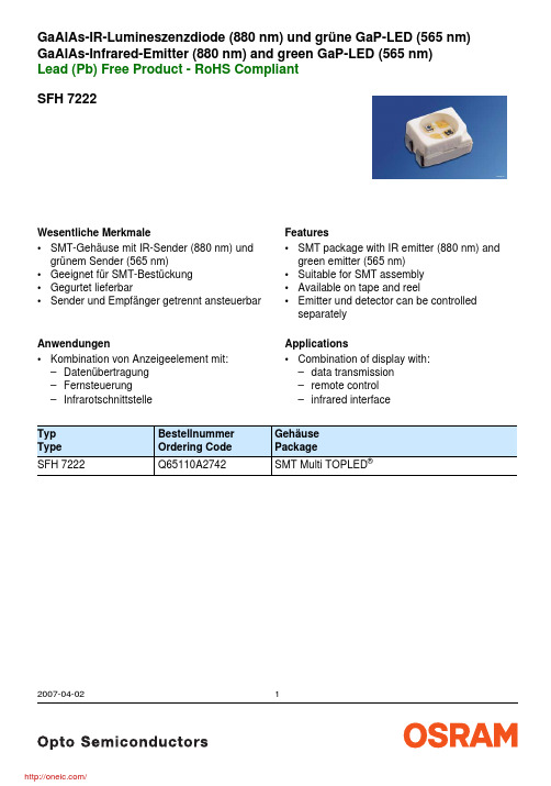
SFH 7222GaAlAs-IR-Lumineszenzdiode (880 nm) und grüne GaP-LED (565 nm) GaAlAs-Infrared-Emitter (880 nm) and green GaP-LED (565 nm)Lead (Pb) Free Product - RoHS Compliant2007-04-021Wesentliche Merkmale•SMT-Gehäuse mit IR-Sender (880 nm) und grünem Sender (565 nm)•Geeignet für SMT-Bestückung •Gegurtet lieferbar•Sender und Empfänger getrennt ansteuerbar Anwendungen•Kombination von Anzeigeelement mit:–Datenübertragung –Fernsteuerung –Infrarotschnittstelle Typ Type Bestellnummer Ordering Code Gehäuse PackageSFH 7222Q65110A2742SMT Multi TOPLED ®Features•SMT package with IR emitter (880 nm) and green emitter (565 nm)•Suitable for SMT assembly •Available on tape and reel•Emitter und detector can be controlled separately Applications•Combination of display with:–data transmission –remote control –infrared interface2007-04-022Hinweis/NotesDie angegebenen Grenzdaten gelten für einen Chip, wenn nicht anders angegeben. The stated maximum ratings refer to one chip, unless otherwise specified.GrenzwerteMaximum Ratings Bezeichnung ParameterSymbol SymbolWert ValueEinheit Unit IREDLEDBetriebstemperaturOperating temperature range T op – 40 … + 100– 40 … + 100°C LagertemperaturStorage temperature range T stg – 40 … + 100– 40 … + 100°C Sperrspannung Reverse voltage V R 55V Durchlassstrom Forward current I F (DC)10030mA Stoßstrom Surge current t p ≤ 10 μs, D = 0I FSM2.50.5AVerlustleistungTotal power dissipationP tot 180100mW WärmewiderstandThermal resistance junction/ambient 1)R th JA 450500K/W WärmewiderstandThermal resistance junction/ambient 2)R th JA650K/W1)nur ein Chip betrieben / only one chip on 2)beide Chips betrieben / both chips onCharacteristicsBezeichnung Parameter SymbolSymbolWertValueEinheitUnitIRED LEDWellenlänge der Strahlung Wavelength of peak emissionI F = 100 mAλpeak880565(I F = 10 mA)nmDominantwellenlänge Dominant wavelengthI F = 10 mAλdom–570nmSpektrale Bandbreite bei 50% von I max Spectral bandwidth at 50% of I maxI F = 100 mAΔλ8025(I F = 10 mA)nmAbstrahlwinkel Half angle ϕ± 60± 60Graddeg.Abmessungen der aktiven Chipfläche Dimensions of the active chip area L × BL × W0.4 × 0.40.25 × 0.25mm2SchaltzeitenSwitching times10%/90%, I F = 100 mA, R L = 50 Ωtr, t f500450, 200nsKapazität CapacitanceV R = 0 V, f = 1 MHzCo2515pFDurchlassspannung Forward voltageI F = 10 mAI F = 100 mA, t p = 20 msI F = 1 A, t p = 100 μsVF–1.5 (≤ 1.8)3.0 (≤ 3.8)2.0 (≤ 2.6)––VSperrstrom, V R = 5 V Reverse current IR0.01 (≤ 1)0.01 (≤ 10)μAGesamtstrahlungsfluss Total radiant fluxI F = 100 mA, t p = 20 msΦe23–mWLichtstärke Luminous intensityI F = 2 mAI V–>0.25mcdTemperaturkoeffizient von I e bzw. Φe Temperature coefficient of I e or ΦeI F = 100 mATCI– 0.5– 0.3%/K2007-04-0232007-04-024IRED Radiation Characteristics I rel = f (ϕ) LED Directional Characteristics S rel = f (ϕ)Temperaturkoeffizient von V F Temperature coefficient of V F I F = 100 mATC V– 2– 1.4mV/KTemperaturkoeffizient von λ Temperature coefficient of λ I F = 100 mATC λ+ 0.250.30 (λpeak ) 0.07 (λdom )nm/KStrahlstärke I e der IRED in Achsrichtung gemessen bei einem RaumwinkelΩ = 0.01 srRadiant Intensity I e of the IRED in Axial Direction at a solid angle of Ω = 0.01 sr Bezeichnung DescriptionSymbol Symbol Werte Values Einheit Unit StrahlstärkeRadiant intensityI F = 100 mA, t p = 20 ms I e min.≥ 4mW/srStrahlstärkeRadiant intensity I F = 1 A, t p = 100 μsI e typ.48mW/srCharacteristics (cont’d)Bezeichnung ParameterSymbol SymbolWert ValueEinheit UnitIREDLED 50˚60˚70˚80˚90˚100˚2007-04-025Forward Current I F = f (V F ) T A = 25 °CI F = f (T)Rel Luminous Intensity I V / I V(10 mA) = f (I F )I Perm. Pulse Handling Capability I F = f (t p ), Duty cycle D = parameter, T AForward Current I F = f (V F) TA= 25 °CIFF A IRelative Luminous IntensityI V / I V(10 mA) = f(I F), T A = 25 °CIPerm. Pulse Handling CapabilityIF= f (tp)Cλ2007-04-026MaßzeichnungPackage OutlinesMaße in mm (inch) / Dimensions in mm (inch).Gehäuse / Package weiß, klarer Verguss / white, clear resinAnschlussbelegung pin configuration 1: Kathode (cathode) 880nm 2: Anode (anode) 880nm 3: Kathode (cathode) 565nm 4: Anode (anode) 565nm2007-04-027Empfohlenes LötpaddesignRecommended Solder PadMaße in mm (inch) / Dimensions in mm (inch).2007-04-028Lötbedingungen Vorbehandlung nach JEDEC Level 2 Soldering Conditions Preconditioning acc. to JEDEC Level 2 Reflow Lötprofil für bleifreies Löten(nach J-STD-020C)Reflow Soldering Profile for lead free soldering(acc. to J-STD-020C)Wellenlöten (TTW)(nach CECC 00802)TTW Soldering(acc. to CECC 00802)2007-04-029OSRAM Opto Semiconductors GmbHWernerwerkstrasse 2, D-93049 Regensburg© All Rights Reserved.The information describes the type of component and shall not be considered as assured characteristics.Terms of delivery and rights to change design reserved. Due to technical requirements components may contain dangerous substances. For information on the types in question please contact our Sales Organization.PackingPlease use the recycling operators known to you. We can also help you – get in touch with your nearest sales office. By agreement we will take packing material back, if it is sorted. You must bear the costs of transport. For packing material that is returned to us unsorted or which we are not obliged to accept, we shall have to invoice you for any costs incurred.Components used in life-support devices or systems must be expressly authorized for such purpose! Critical components 1 , may only be used in life-support devices or systems 2 with the express written approval of OSRAM OS.1 A critical component is a component usedin a life-support device or system whose failure can reasonably be expected to cause the failure of that life-support device or system, or to affect its safety or effectiveness of that device or system.2 Life support devices or systems are intended (a) to be implanted in the human body, or (b) to support and/or maintain and sustain human life. If they fail, it is reasonable to assume that the health of the user may be endangered.2007-04-0210分销商库存信息: OSRAMSFH 7222-Z。