MAX7418中文资料
MAX038资料中文

高频信号发生器_______________概述MAX038是一种只需极少外围电路就能实现高 频、高精度输出三角波、锯齿波、正弦波、方波 和脉冲波的精密高频函数发生器芯片。
内部提供 的2.5V 基准电压和一个外接电阻和电容可以控制 输出频率范围在0.1Hz 到20MHz 。
占空比可在较大 的范围内由一个±2.3V的线性信号控制变化,便 于进行脉冲宽度调制和产生锯齿波。
频率调整和 频率扫描可以用同样的方式实现。
占空比和频率 控制是独立的。
通过设置2个TTL 逻辑地址引脚合适的逻辑电 平,能设定正弦波,方波或三角波的输出。
所有 波形的输出都是峰-峰值为±2VP -P 的信号。
低阻 抗输出能力可以达到±20mA。
____________________________性能o 频率调节范围:0.1Hz 到20MHzo 三角波, 锯齿波, 正弦波, 方波和脉冲波 o 频率和占空比独立可调 o 频率扫描范围:350:1 o 可控占空比:15%到85% o 低阻抗输出缓冲器: 0.1Ω o 低失真正弦波: 0.75% o 低温度漂移: 200ppm/°C______________型号信息TTL 逻辑地址引脚SYNC 从内部振荡器输出占 空比固定为50%的信号,不受其它波占空比的影 响,从而同步系统中其它振荡器。
内部振荡器 允许被连接着相位检波器输入端(PDI )的外部 TTL 时钟同步。
型号 MAX038CPP MAX038CWP MAX038C/D MAX038EPP MAX038EWP工作温度 0°C 到 +70°C 0°C 到 +70°C 0°C 到 +70°C -40°C 到 +85°C -40°C 到 +85°C引脚--封装 20 Plastic DIP 20 SO Dice* 20 Plastic DIP 20 SO.__________________应用精密函数信号发生器 压控振荡器 频率调制器*Contact factory for dice specifications.__________________引脚图脉宽调制器 锁相环 频率合成器FSK 发生器(正弦波和方波)________________________________________________________________ Maxim Integrated Products1For free samples & the latest literature: , or phone 1-800-998-8800. For small orders, phone 408-737-7600 ext. 3468MAX038高频信号发生器图1. 内部结构及基本工作电路_______________ 详细说明MAX038是一种高频函数信号发生器,它可以使 用最少的外部元件而产生低失真正弦波,三角波, 锯齿波,方波(脉冲波)。
MAX7221的资料

MAX72211 概述MAX7221 是Maxim(美信)公司专为LED 显示驱动而设计生产的串行接口八位LED 显示驱动芯片.该芯片包含有七段译码器、位和段驱动器、多路扫描器、段驱动电流调节器、亮度脉宽调节器及多个特殊功能寄存器.该芯片采用串行接口方式,可以很方便地和单片机相连,未经扩展最多可用于 8 位数码显示或 64 段码显示.经实际使用发现,该芯片具有占用单片机 I/O 口少(仅三线)、显示多样、可靠性高、简单实用、编程灵活方便的特点.2 MAX7221 功能简介MAX7221 的功能特点(1)10MHz 的串行接口;(2)BCD 译码/非译码模式选择;(3)耗电仅150uA 的省电模式(显示关闭);(4)数字和模拟双重亮度控制;(5)SPI、QSPI、Microwire 等多种串行接口;(6)显示位数可方便地进行扩展.MAX7221 引脚介绍(见图1)Din 脚,串行数据输入端,数据存入内部16 位移位寄存器.DIG0~DIG7 脚,8 位共阴极数码管的控制输入端,显示关闭时输出高电平.GND 脚,接地端,4 和9 脚都要接地.CS 脚,片选输入端,当CS=0 时,串行数据存入移位寄存器,当CS 为上升沿时锁存最后16 位数据.CLK 脚,串行时钟输入端,最高频率10MHz,在时钟上升沿数据移位存入内部移位寄存器,当时钟下降沿时,数据由Dout 输出,CLK 输入仅当CS=0 时有效.SEGA~SEGG,SEGDP 脚,数码管七段驱动和小数点驱动端,关闭显示时各段驱动输出为高电平.收稿日期:2003-11-20作者简介:张华林(1973-),男,福建诏安县人,讲师,学士.Iset 脚,连接到Vdd 的电阻连接端,用来模拟设定各段驱动电流.Vdd 脚,5V 正电压输入端.Dout 脚,串行数据输出端,数据由 Din 输入,经个时钟延迟后由 Dout 引脚输出,此引脚用来扩展MAX7221.MAX7221 功能串行数据输入和控制寄存器串行数据输入输出时CS 必须为低电平,串行数据由Din 送入一个16 位的数据包,并在每个时钟上升沿时存入内部 16 位移位寄存器.数据经个周期后,在时钟的下降沿由 Dout 引脚输出.16 位数据D0~D15 的排列见表~D7 包含数据,D8~D11 包含寄存器地址,D12~D15 为未定义位,芯片最先接收D15 位.控制寄存器的地址图见表2.表1表2省电模式MAX7221 允许工作在省电模式(显示关闭,见表3),在该模式下,供电电流可降低到150uA.器件在这种模式下上电时,250us 内即可进入正常工作模式.在测试状态下,省电模式被屏蔽.表3译码/非译码模式译码模式寄存器可以设置对每一位数字的BCD 译码模式或非译码模式,寄存器的每一位对应一个数字,高电平代表译码,低电平代表旁路译码器.见表4.当芯片处于译码模式时,数据位只有D0~D3 有效,D4~D6 位为无效位,D7 为小数点位,见表5.当芯片处于非译码模式时,数据D0~D7 位对应8 个笔划段,见表6.表5表6亮度控制寄存器本芯片允许由外加在Vdd 和Iset 之间的电阻Rset 调节LED 亮度,Rset 阻值至少为,它也允许由亮度控制寄存器进行设置,通过设置每一笔划的扫描脉冲占空比达到调整亮度的目的,见表7.扫描位数控制寄存器扫描位数控制寄存器可以设置显示1~8 位(见表8),多路扫描器在显示8 位时典型的扫描频率为 800Hz.显示位数减少时,扫描频率上升为 8f/N(f 为扫描频率,N 为显示位数).当显示位数为3 位、2 位、1 位时,Rset 应至少增大为15K、20K、40K.表8显示测试模式和空操作模式显示测试寄存器操作有两种模式:正常模式和显示测试模式(见表9).显示测试时屏蔽所有功能设置,全部8 位的每一笔划的扫描脉冲占空比均为15/16.空操作模式用于芯片扩展,后面的芯片要显示的数据经过前面的芯片时,前面的芯片应处于空操作模式.表93 MAX7221 与PIC 单片机的连接MAX7221 与 PIC16C73 单片机的接口电路如图 2 所示,该电路是某型号打码机的显示部分电路,U1、U2、U3 分别用来显示打码速度、打码碳带温度、打码位置.U1、U2、U3 共占用 7 个数码管,另有4 个指示灯,分别为工作指示、测试指示、温度过高报警指示、碳带用完报警指示.PIC 单片机的RC3、RC4、RC5 分别接MAX7221 的CLK、DATAIN、CS 引脚.本文介绍的显示电路应用于某型号打码机,经实践证明,其显示简单,运行可靠.该芯片还A可以广泛应用于段曲线显示、工业控制、LED 矩阵显示等.图1G4DIG510 G5DIG6 5G6DIG78 +5LED1图2LED3。
MAX488中文资料
74系列芯片简介

74248/249、74LS248/249BCD—七段译码器/驱动器
有驱动灯缓冲器的有效高电平输出;有灯测试装置;前沿/后沿零熄灭;能调节灯光强度;248为有升压电阻,249为集电极开路输出,引脚图与74246相同。
功能表
74251、74LS251、74F251、74ALS251、74S251、74HC2518选1数据选择器/驱动器(三态)
74290、74LS290十进制计数器
二分频和五分频;有门置零及门置9输入。电性能和功能分别与7490A和74LS290A相同,只是改变了引线排列。
BCD计数时序
二—五混合进制
复位/计数功能表
74 LS292、74HC292可编程分频器/数字定时器(最大231)
链式计数分频;从22的231数字程序。
有多路输入/输出线;四种工作模式,保持(存贮)左移、右移、送数;三态输出直接驱动总线;74LS299与相电路相似, 但有异步复位。
功能表
74LS324压控振荡器(双相输出、允许控制)
输出频率由外接元件决定;可在30~120Hz之间任一频率下工作;若在频控和范围输入端加2伏电压,则输出频率近似为(10-4CEXT)有互补输出。
功能表
74192、74L192、74LS192、74F192、74 ALS192、74 HC192、74 C192可预置BCD十进制同步可逆计数器(双时钟带清除)
功能表
74193、74L193、74LS193、74F193、74 ALS193、74 HC193、74 C193可预置4位二进制同步可逆计数器(双时钟带清除)引脚图与74192相同。
74系列芯片简介
默认分类2009-05-25 11:25:01阅读406评论0字号:大中小
MAXIM MAX5417 5418 5419 说明书

________________________________概述MAX5417/MAX5418/MAX5419是非易失、线性数字电位器,与机械电位器功能相似,但可通过简单的2线数字接口控制,允许多个器件进行通信。
每个器件具有分离电位器或可变电阻的功能,具有256个抽头点。
这些器件内置非易失EEPROM ,用于存储滑动端的位置,上电时进行初始化处理。
快速模式I 2C TM 兼容接口允许400kbps 的通信速率,在许多应用场合可有效减小电路板面积,简化电路连接。
每个器件有一个工厂预置地址,有四种地址选择(见选择指南),配合地址选择输入,共提供八个唯一的地址组合。
MAX5417/MAX5418/MAX5419提供了三个标称阻值:50kΩ(MAX5417)、100kΩ(MAX5418)和200kΩ(MAX5419)。
标称电阻的端到端温度系数为35ppm/°C, 比率温度系数仅为5ppm/°C ,非常适合低温漂可变电阻的应用,如低漂移、可编程增益放大器。
MAX5417/MAX5418/MAX5419采用3mm x 3mm 、8引脚TDFN 封装,工作在-40°C 至+85°C 扩展级温度范围。
________________________________应用替代机械电位器低漂移可编程增益放大器音量控制液晶显示屏(LCD)对比度控制________________________________特性♦上电后从非易失存储器调用滑动端位置♦微型3mm x 3mm 、8引脚TDFN 封装♦端到端电阻温度系数:35ppm/°C ♦比率温度系数:5ppm/°C ♦阻值:50k Ω/100k Ω/200k Ω♦快速I 2C 兼容串行接口♦500nA (典型值)静态电流♦单电源+2.7V 至+5.25V 供电♦256抽头♦分压模式下DNL 为:±0.5 LSB ♦分压模式下INL 为:±0.5 LSBMAX5417/MAX5418/MAX5419256抽头、非易失、I 2C 接口数字电位器________________________________________________________________Maxim Integrated Products1功能图19-3185; Rev 2; 8/04本文是Maxim 正式英文资料的译文,Maxim 不对翻译中存在的差异或由此产生的错误负责。
MAX038中文

MAX038芯片中文资料及在波形发生器中的应用(1)简介:波形发生器的应用范围很广。
在分析检测设备、超声设备、医疗设备及通讯设备中广泛应用。
函数发生器作为信号激励源,其参数精度是设计时应考虑的重要因素 ...波形发生器的应用范围很广。
在分析检测设备、超声设备、医疗设备及通讯设备中广泛应用。
函数发生器作为信号激励源,其参数精度是设计时应考虑的重要因素。
常用的波形产生电路有RC震荡电路、LC震荡电路、文氏震荡电路以及由555芯片构成的震荡电路等,但这些震荡电路由于核心芯片、选频及限幅元件特性的限制,在幅频精度方面或多或少的存在着不稳定或实现电路复杂等情况。
如果需要实现波形变换、幅频大小调整以及提高幅频的稳定度,设计的外围电路将会变得更为复杂。
由MAX038设计组成的波形产生电路能够输出幅频精度很高且易于调整的波形信号,在电路参数要求苛刻的工作场合能够得到较好的应用。
1 芯片功能介绍1.1 MAX038芯片的性能特点MAX038CPP芯片采用20引脚DIP封装,引脚图如图1所示。
各引脚功能简述如下:REF:芯片内部2.5 V参考电压输出;GND:模拟地;A1,A0:输出波形选择,TTL/CMOS兼容;COSC:内部震荡器外接电容;FADJ,DADJ:输出频率、占空比调节;IIN:震荡频率控制器电流输入;PDI,PDO:内部鉴相器输入、输出;SYNC:同步信号输出,允许内部震荡器与外电路同步;DGND,DV+:内部数字电路电源;V+,V-:MAX038电源(+5 V,-5 V);OUT:波形输出端。
MAX038芯片附加少许外围电路就能够产生三角波、锯齿波、正弦波、方波、矩形脉冲波形。
该芯片具有如下的功能特点:(1)输出频率范围:0.1~20 MHz,最高可达40 MHz:(2)输出波形占空比(15%~85%)独立可调,占空比可由DADJ端调整,如果DADJ 端接地,则输出占空比为50%;(3)具有低输出阻抗的输出缓冲器,输出阻抗的典型值为0.1 Ω;(4)备有TTL兼容的独立同步信号SYNC(方波输出,固定占空比为50%),方便组建频率合成器系统;(5)低温度漂移。
MAX3841中文资料

PARAMETER
SYMBOL
CONDITIONS
MIN TYP MAX UNITS
Core Supply Current Data Rate
ICC
Excluding CML termination currents
(Note 1)
65
90
mA
0
12.5 Gbps
CML Input Differential CML Input Common Mode
Termination Currents)
Ordering Information
PART
TEMP RANGE
MAX3841ETG -40°C to +85°C
PINPACKAGE
24 Thin QFN
PKG. CODE
T2444-1
Pin Configuration appears at end of data sheet.
12
dB
CML Output Differential CML Output Termination
VOUT
(Note 2) Single ended
400
500
42.5
50
600 57.5
mVP-P Ω
CML Output Transition Time Deterministic Jitter Random Jitter Propagation Delay
Note 4: Measured at 9.953Gbps using a pattern of 100 ones, 27 - 1 PRBS, 100 zeros, 27 - 1 PRBS, and at 12.5Gbps using a ±K28.5 pattern. VCC_IN = VCC_OUT = 1.8V, and VIN = 400mVP-P differential.
MAX1978中文数据手册

用于Peltier模块的集成温度控制器概论MAX1978 / MAX1979是用于Peltier热电冷却器(TEC)模块的最小, 最安全, 最精确完整的单芯片温度控制器。
片上功率FET和热控制环路电路可最大限度地减少外部元件, 同时保持高效率。
可选择的500kHz / 1MHz开关频率和独特的纹波消除方案可优化元件尺寸和效率, 同时降低噪声。
内部MOSFET的开关速度经过优化, 可降低噪声和EMI。
超低漂移斩波放大器可保持±0.001°C的温度稳定性。
直接控制输出电流而不是电压, 以消除电流浪涌。
独立的加热和冷却电流和电压限制提供最高水平的TEC保护。
MAX1978采用单电源供电, 通过在两个同步降压调节器的输出之间偏置TEC, 提供双极性±3A输出。
真正的双极性操作控制温度, 在低负载电流下没有“死区”或其他非线性。
当设定点非常接近自然操作点时, 控制系统不会捕获, 其中仅需要少量的加热或冷却。
模拟控制信号精确设置TEC 电流。
MAX1979提供高达6A的单极性输出。
提供斩波稳定的仪表放大器和高精度积分放大器, 以创建比例积分(PI)或比例积分微分(PID)控制器。
仪表放大器可以连接外部NTC或PTC热敏电阻, 热电偶或半导体温度传感器。
提供模拟输出以监控TEC温度和电流。
此外, 单独的过热和欠温输出表明当TEC温度超出范围时。
片上电压基准为热敏电阻桥提供偏置。
MAX1978 / MAX1979采用薄型48引脚薄型QFN-EP 封装, 工作在-40°C至+ 85°C温度范围。
采用外露金属焊盘的耐热增强型QFN-EP封装可最大限度地降低工作结温。
评估套件可用于加速设计。
应用光纤激光模块典型工作电路出现在数据手册的最后。
WDM, DWDM激光二极管温度控制光纤网络设备EDFA光放大器电信光纤接口ATE特征♦尺寸最小, 最安全, 最精确完整的单芯片控制器♦片上功率MOSFET-无外部FET♦电路占用面积<0.93in2♦回路高度<3mm♦温度稳定性为0.001°C♦集成精密积分器和斩波稳定运算放大器♦精确, 独立的加热和冷却电流限制♦通过直接控制TEC电流消除浪涌♦可调节差分TEC电压限制♦低纹波和低噪声设计♦TEC电流监视器♦温度监控器♦过温和欠温警报♦双极性±3A输出电流(MAX1978)♦单极性+ 6A输出电流(MAX1979)订购信息* EP =裸焊盘。
课程设计-- 位数字电压表

课程设计-- 位数字电压表┊┊┊┊┊┊┊┊┊┊┊┊┊装┊┊┊┊┊订┊┊┊┊┊线┊214位数字电压表[摘要] 数字电压表(DVM )是将被测的电压模拟量自动转换成开关量,然后进行数字编码、译码,以数字形式显示出来的一种电测仪表,本文所介绍的是采用ICL7135高精度AD转换电路,将模拟量输入电压变换为数字量,通过芯片74LS47译码显示到数码管上,测量范围为直流0 —±1.9999伏。
该电路外接正5v作为电源,用74hc04进行负变,为ICL7135提供-5v电压,并用时钟芯片ICM7556组建了一个产生脉冲的震荡电路,为电路提供时钟信号。
[关键字] AD转换;译码;时钟信号;数字电压表┊┊┊┊┊┊┊┊┊┊┊┊┊装┊┊┊┊┊订┊┊┊┊┊线┊Four And a Half Digital Voltmeter[Abstract] Digital voltage meter ( DVM ) is the measured voltage simulation quantity automatically converted to the switch, and then digital encoding, decoding, displayed in digital form out of a measuring instrument, described in this article is the use of ICL7135 high precision AD conversion circuit, the analog input voltage into digital quantity, through the chip 74LS47 decoding display to digital control, the measuring range is 0± 1.9999 volts dc. The circuit of external 5V as power source, with 74hc04 were negative, as ICL7135 -5v voltage, and the clock chip ICM7556 formed a pulse oscillating circuit, a clock signal supplying circuit for.[Key words]AD conversion; decoding; Clock signal ;Digital voltage meter┊┊┊┊┊┊┊┊┊┊┊┊┊装┊┊┊┊┊订┊┊┊┊┊线┊目录第1章前言 (1)1.1 数字电压表的特点及发展趋势 (1)1.1.1数字电压表的特点 (1)1.1.2数字电压表的发展趋势 (1)1.2 设计要求及方案选择 (2)1.2.1设计要求 (2)1.2.2方案选择 (2)第2章数字电压表单元电路设计 (4)2.1 A/D转换单元电路设计 (4)2.1.1 A/D转换器ICL7135的功能介绍 (4)2.1.2 A/D转换电路设计 (6)2.2 时钟产生单元电路设计 (6)2.2.1 ICM7556功能介绍 (6)2.2.2 ICM7556组成的多谐振荡器 (7)2.3.1驱动电路设计 (9)2.3.2译码电路设计 (11)2.3.3显示电路设计 (12)2.4 电源单元电路设计 (12)2.4.1正电源电路设计 (12)2.4.2负电源电路设计 (13)第3章调试要点及测试方法 (15)3.1 调试要点及测试方法 (15)3.2 故障及排除 (15)第4章设计总结 (16)4.1 设计总结 (16)4.2 设计心得 (16)参考文献 (17)┊┊┊┊┊┊┊┊┊┊┊┊┊装┊┊┊┊┊订┊┊┊┊┊线┊第1章前言1.1 数字电压表的特点及发展趋势1.1.1数字电压表的特点数字电压表(DVM )是将被测的电压模拟量自动转换成开关量,然后进行数字编码、译码,以数字形式显示出来的一种电测仪表,它具有如下主要特点:(1)准确度高:目前可达到10^-6数量级,因此用它代替直读仪表,可大大提高测量精度。
max038资料及应用
高频函数信号发生器MAX038及其应用作者:李琳来源:网络目前广泛应用的函数发生器芯片是ICL8038(国产5G8038),他的主要技术指标是最高振荡频率仅为100 kHz,而且三种输出波形从不同的引脚输出,使用很不方便。
MAX038是ICL8038的升级产品,他的最高振荡频率可达40 MHz,而且由于在芯片内采用了多路选择器,使得三种输出波形可通过编程从同一个引脚输出,输出波形的切换时间可在0.3μs内完成,使用更加方便。
1 MAX038芯片介绍MAX038是MAXIM公司生产的一个只需要很少外部元件的精密高频波形产生器,在适当调整其外部控制条件时,它可以产生准确的高频方波、正弦波、三角波、锯齿波等信号,这些信号的峰峰值精确地固定在2V,频率从0.1Hz~20MHz连续可调,方波的占空比从10%~90%连续可调。
通过MAX038的A0、A1引脚上电平的不同组合,可以选择不同的输出波形类型。
其性能特点如下:(1) 0.1 Hz~20 MHz工作频率范围;(2) 15%~85%可变的占空比;(3) 低阻抗输出缓冲器:0.1;(4) 低失真正弦波:0.75%;(5) 低温度漂移:200 ppm/℃。
MAX038引脚排列如图所示各引脚功能如图所示:Max038内部电路,如图:2 MAX038芯片使用方法2.1 波形选择MAX038可以产生正弦波、方波或三角波。
具体的输出波形由地址A0和A1的输入数据进行设置,如表1所示。
波形切换可通过程序控制在任意时刻进行,而不必考虑输出信号当时的相位。
2.2 波形调整2.2.1 输出频率的调整输出频率调整方式分为粗调和细调两种方法:粗调取决于IIN引脚的输入电流IIN,COSC引脚的电容量CF(对地)以及FADJ引脚上的电压。
当VFADJ=0 V时,输出的中心频率f0为:fo(MHz)=Iin(μA)÷COSC (pF) 。
当IIN在10~400μA 这个范围变化时,电路可以获得最佳的工作性能。
最全ua741中文资料

更多同类免费资料下载:淘宝小店:UA741中文资料uA741M,uA741I,uA741C(单运放)是高增益运算放大器,用于军事,工业和商业应用.这类单片硅集成电路器件提供输出短路保护和闭锁自由运作。
这些类型还具有广泛的共同模式,差模信号范围和低失调电压调零能力与使用适当的电位。
uA741M,uA741I,uA741C芯片引脚和工作说明:1和5为偏置(调零端),2为正向输入端,3为反向输入端,4接地,6为输出,7接电源 8空脚温度等级 Package 封装Part Number 零件型号 Temperature Range 工作温度范围 N D UA741C 0℃ - +70℃ • • UA741I -40℃ - +105℃ • • UA741M-55℃ - +125℃• •例如 : UA741CNABSOLUTE MAXIMUM RATINGS 最大额定值 Symbol 符号 Parameter 参数 UA741MUA741I UA741CUnit 单位 VCC Supply voltage 电源电压±22 V Vid Differential Input Voltage 差分输入电压±30 V Vi Input Voltage 输入电压±15 V PtotPower Dissipation 功耗500mWToperOutput Short-circuit Duration 输出短路持续时间 Infinite 无限制Operating Free-air Temperature Range 工作温度 -55 to +125 -40 to +105 0 to +70 ℃ELECTRICAL CHARACTERISTICS VCC = ±15V, Tamb = +25°C (unless otherwise specified) 电气特性虚拟通道连接= ± 15V , Tamb = 25 ℃(除非另有说明)上升时间单位增益Kov Overshoot Vi=20mV,RL=2KΩ,CL=100pF,unity Gain超虚拟单位增益- 5 -%Ri Input Resistance 输入阻抗 2 -MΩGBP Gain Bandwith Pro duct Vi = 10mV, RL =2KΩ,CL = 100pF,f =100kHz 带宽增益1 -MHzTHD Total Harmonic Distortion f = 1kHz, Av = 20dB,RL=2KΩ,Vo=2Vpp, CL=100pF,Tamb=+25℃总谐波失真--%en Equivalent Input Noise Voltage f=1kHz,Rs=100Ω 等效输入噪声电压-23 -nV √Hz¢m Phase Margin 相位裕度-50 -Degrees UA741/ LM741应用电路:图6 12V的电池监视器图7 低功耗放大器图8 741驱动三极管的5瓦功率放大器图9 自动感光电路图图10 夜间自动感光电路图图11 声音探测器图12 数字/模拟输出接口电路更多同类免费资料下载:淘宝小店:。
MAX1241中文资料datasheet

MAX1240 / MAX1241 采用 8 引脚封装的低 功耗、12 位模数转换器转换器(ADC)。 MAX1240 采 用 + 2.7V 至 + 3.6V 的 电 源 供 电,MAX1241 采用单电源供电范围是+ 2.7V 至+ 5.25V。这两款设备都具有 7.5μs 的功 能 逐次逼近 ADC,快速跟踪/保持(1.5μs), 片上时钟和高速 3 线串行接口。 在 73ksps 的 最 大 采 样 速 度 下 , 功 耗 仅 为 37mW(VDD = 3V)。2μA 关断模式以较 慢的吞吐率来降低功耗。 MAX1240 具 有 内 部 2.5V 参 考 电 压 , 而 MAX1241 需要外部参考电 压。MAX1241 接受从 0V 到VREF 和参考信号输入范围包括 正电源轨。外部的时钟从 3 线接口访问数据, 它直接连接到标准微控制器的 I/O 港口。该 接口与 SPI™,QSPI™和 MICROWIRE™兼容。 该接卓越的交流特性和极低的功耗,易于使 用和小封装尺寸,使这些转换器成为远程传 感器和数据采集应用的理想之选,或者是要 求降低功耗和对空间有要求的电路的最好 选择。MAX1240/MAX1241 采用 8 引脚 PDIP 和 SO 封装。
兑换率
转换时间 跟踪/保持采集时 间 转换时间 吞吐率 光圈抖动
tCONV
t ACQ
t APR
fSCLK=2.1MHz 图8
5.5
7.5
us
1.5
us
73
ksps
30
ns
<50
ps
模拟输入
输入电压范围 输入电容
0
VREF V
16
pF
电源要求
DM7417中文资料
© 2000 Fairchild Semiconductor Corporation DS006505August 1986Revised February 2000DM7417 Hex Buffers with High Voltage Open-Collector OutputsDM7417Hex Buffers with High Voltage Open-Collector OutputsGeneral DescriptionThis device contains six independent gates each of which performs a buffer function. The open-collector outputs require external pull-up resistors for proper logical opera-tion.Pull-Up Resistor EquationsWhere: N 1 (I OH ) = total maximum output high currentfor all outputs tied to pull-up resistorN 2 (I IH ) = total maximum input high current for all inputs tied to pull-up resistorN 3 (I IL ) = total maximum input low current for all inputs tied to pull-up resistorOrdering Code:Devices also available in T ape and Reel. Specify by appending the suffix letter “X” to the ordering code.Connection Diagram Function TableY = AH = HIGH Logic Level L = LOW Logic LevelOrder Number Package NumberPackage DescriptionDM7417M M14A 14-Lead Small Outline Integrated Circuit (SOIC), JEDEC MS-012, 0.150 Narrow DM7417NN14A14-Lead Plastic Dual-In-Line Package (PDIP), JEDEC MS-001, 0.300 WideInput Output A Y L L HH 2D M 7417Absolute Maximum Ratings (Note 1)Note 1: The “Absolute Maximum Ratings” are those values beyond which the safety of the device cannot be guaranteed. The device should not be operated at these limits. The parametric values defined in the Electrical Characteristics tables are not guaranteed at the absolute maximum ratings.The “Recommended Operating Conditions” table will define the conditions for actual device operation.Recommended Operating ConditionsElectrical Characteristicsover recommended operating free air temperature range (unless otherwise noted)Note 2: All typicals are at V CC = 5V, T A = 25°C.Switching Characteristicsat V CC = 5V and T A = 25°C Supply Voltage 7V Input Voltage 5.5V Output Voltage15VOperating Free Air Temperature Range 0°C to +70°CStorage Temperature Range−65°C to +150°CSymbol ParameterMin Nom Max Units V CC Supply Voltage4.7555.25V V IH HIGH Level Input Voltage 2V V IL LOW Level Input Voltage 0.8V V OH HIGH Level Output Voltage 15V I OL LOW Level Output Current 40mA T AFree Air Operating Temperature070°CSymbol ParameterConditionsMinTyp Max Units (Note 2)V I Input Clamp Voltage V CC = Min, I I = −12 mA −1.5V I CEX HIGH Level V CC = Min, V O = 15V 250µAOutput Current V IH = Min V OLLOW Level V CC = Min, I OL = Max0.7Output VoltageV IL = MaxVI OL = 16 mA, V CC = Min 0.4I I Input Current @ Max V CC = Max, V I = 5.5V1mA Input VoltageI IH HIGH Level Input Current V CC = Max, V I = 2.4V 40µA I IL LOW Level Input CurrentV CC = Max, V I = 0.4V −1.6mA I CCH Supply Current with Outputs HIGH V CC = Max 2941mA I CCLSupply Current with Outputs LOWV CC = Max2130mASymbol ParameterConditionsMinMax Units t PLH Propagation Delay Time C L = 15 pF 10ns LOW-to-HIGH Level Output R L = 110Ωt PHLPropagation Delay Time 30nsHIGH-to-LOW Level Output DM7417Physical Dimensions inches (millimeters) unless otherwise noted14-Lead Small Outline Integrated Circuit (SOIC), JEDEC MS-012, 0.150 NarrowPackage Number M14A4D M 7417 H e x B u f f e r s w i t h H i g h V o l t a g e O p e n -C o l l e c t o r O u t p u t sPhysical Dimensions inches (millimeters) unless otherwise noted (Continued)14-Lead Plastic Dual-In-Line Package (PDIP), JEDEC MS-001, 0.300 WidePackage Number N14AFairchild does not assume any responsibility for use of any circuitry described, no circuit patent licenses are implied and Fairchild reserves the right at any time without notice to change said circuitry and specifications.LIFE SUPPORT POLICYFAIRCHILD’S PRODUCTS ARE NOT AUTHORIZED FOR USE AS CRITICAL COMPONENTS IN LIFE SUPPORT DEVICES OR SYSTEMS WITHOUT THE EXPRESS WRITTEN APPROVAL OF THE PRESIDENT OF FAIRCHILD SEMICONDUCTOR CORPORATION. As used herein:1.Life support devices or systems are devices or systems which, (a) are intended for surgical implant into the body, or (b) support or sustain life, and (c) whose failure to perform when properly used in accordance with instructions for use provided in the labeling, can be rea-sonably expected to result in a significant injury to the user. 2. A critical component in any component of a life support device or system whose failure to perform can be rea-sonably expected to cause the failure of the life support device or system, or to affect its safety or effectiveness.。
MAXFILTERBRD+;中文规格书,Datasheet资料

_______________________________________________________________ Maxim Integrated Products 1For pricing, delivery, and ordering information, please contact Maxim Direct at 1-888-629-4642, MAXFILTERBRDEvaluates: MAX7408–MAX7415/MAX7418–MAX7425General DescriptionThe MAXFILTERBRD is an unpopulated PCB design to evaluate the MAX7408–MAX7415/MAX7418–MAX7425 5th-order, lowpass, switched-capacitor filters (SCFs).Contact the factory for free samples of the pin-compat-ible MAX7408–MAX7415/MAX7418–MAX7425 SCFs to evaluate these devices.FeaturesS CLK Pad for External Clock Frequency S Lead(Pb)-Free and RoHS Compliant S Proven PCB LayoutOrdering InformationComponent SupplierPart Selection TableComponent List(Suggested Components)19-4884; Rev 0; 8/09+Denotes lead(Pb)-free and RoHS compliant.Note: Contact the factory to order a free sample of any of the SCF parts.µMAX is a registered trademark of Maxim Integrated Products, Inc.Note: Indicate that you are using the MAXFILTERBRD when contacting this component supplier.PART TYPE MAXFILTERBRD+EV KitPARTOPERATING VOLTAGEFILTER TYPEMAX7408CUA+5V Elliptic MAX7409CUA+5V Bessel MAX7410CUA+5V Butterworth MAX7411CUA+5V Elliptic MAX7412CUA+3V Elliptic MAX7413CUA+3V Bessel MAX7414CUA+3V Butterworth MAX7415CUA+3V Elliptic MAX7418CUA+5V Elliptic MAX7419CUA+5V Bessel MAX7420CUA+5V Butterworth MAX7421CUA+5V Elliptic MAX7422CUA+3V Elliptic MAX7423CUA+3V Bessel MAX7424CUA+3V Butterworth MAX7425CUA+3VEllipticDESIGNATIONQTY DESCRIPTIONC1Not installed, 47pF Q 5%, 50V C0G ceramic capacitor (0805)Murata GRM2165C1H470J or similarC20Not installed, 2200pF Q 5%, 50V C0G ceramic capacitor (0805)Murata GRM2165C1H222J or similarC3, C40Not installed, 0.1F F Q 10%, 16V X7R ceramic capacitors (0603)Murata GCM188R71C104K or similarJU1, JU20Not installed, 2-pin headers—shorted by PC traceR1Not installed, 10k I Q 1% resistor (0805)U10Not installed, lowpass SCF (8 F MAX M )See the Part Selection Table —1PCB: MAXFILTERBRD+SUPPLIERPHONE WEBSITEMurata Electronics North America, Inc.770-436-1300MAXFILTERBRD E v a l u a t e s : M A X 7408–M A X 7415/M A X 7418–M A X 74252 ______________________________________________________________________________________Quick StartRequired Equipment• MAXFILTERBRD• Suggested components (see Component List )• 5V or 3V DC power supply (depending on the IC installed)• Function generator (e.g., HP 33120A)• 2-channel digital oscilloscope (e.g., Tektronix TDS3012)ProcedureCaution: Do not turn on power supply until all connec-tions are completed.1) I nstall all suggested components shown in theComponent List onto the MAXFILTERBRD.2) I f the installed IC is the MAX7408–MAX7411 orMAX7418–MAX7421, connect the positive terminal ofthe 5V supply to the VDD pad and the negative termi-nal of the supply to the GND pad closest to the VDDpad. If the installed IC is the MAX7412–MAX7415 or MAX7422–MAX7425, connect the positive terminal of the 3V supply to the VDD pad and the negative terminal of the supply to the GND pad closest to the VDD pad (see Figure 1). Set the function generator to 4V P-P max, 2.2V offset (typ), and 1kHz sine wave, and connect the signal to the IN pad.3) C onnect the first channel of the oscilloscope to theIN pad.4) C onnect the second channel of the oscilloscope tothe OUT pad.5) C onnect the oscilloscope’s ground probe to any GNDpads.6) Turn on the power supply.7) Verify the output on the OUT pad.Figure 1. Filter Evaluation Test Block DiagramMAXFILTERBRDEvaluates: MAX7408–MAX7415/MAX7418–MAX7425_______________________________________________________________________________________ 3Detailed Description of HardwareThe MAXFILTERBRD is an unpopulated PCB design to evaluate the MAX7408–MAX7415/MAX7418–MAX7425 5th-order, lowpass SCFs.Internal ClockThe MAXFILTERBRD uses the internal oscillator when a capacitor is installed on C1. Refer to corresponding installed IC data sheet.For the MAX7409/MAX7410/MAX7413/MAX7414, the frequency can be altered using the following formula:f OSC (kHz) = k/C1 (pF)where k = 30 x 103 and f OSC is the internal oscillator frequency.For the MAX7408/MAX7411/MAX7412/MAX7415, k = 27 x 103.For the MAX7418/MAX7421/MAX7422/MAX7425, k = 87 x 103.For the MAX7419/MAX7420/MAX7423/MAX7424, k = 110 x 103.External ClockAn external clock that matches the specification of the corresponding IC data sheet can be used by cutting the trace of jumper JU2. Drive the CLK pin with a CMOS gate powered from 0 to VDD. Apply the clock signal to the CLK pad.ShutdownThe MAXFILTERBRD is configured for normal operation once the desired IC is installed. The desired IC enters shutdown by cutting the trace of jumper JU1 and driving the IC SHDN pin low through the side of the jumper that is still connected to the part.MAXFILTERBRDE v a l u a t e s : M A X 7408–M A X 7415/M A X 7418–M A X 74254 ______________________________________________________________________________________Figure 2. MAXFILTERBRD SchematicMaxim cannot assume responsibility for use of any circuitry other than circuitry entirely embodied in a Maxim product. No circuit patent licenses are implied. Maxim reserves the right to change the circuitry and specifications without notice at any time.Maxim Integrated Products, 120 San Gabriel Drive, Sunnyvale, CA 94086 408-737-7600 5© 2009 Maxim Integrated ProductsMaxim is a registered trademark of Maxim Integrated Products, Inc.MAXFILTERBRDEvaluates: MAX7408–MAX7415/MAX7418–MAX7425Figure 3. MAXFILTERBRD Component Placement Guide—Component SideFigure 5. MAXFILTERBRD PCB Layout—Solder SideFigure 4. MAXFILTERBRD Component PCB Layout—Component Side Figure 6. MAXFILTERBRD Component Placement Guide—Solder Side分销商库存信息: MAXIM MAXFILTERBRD+。
MAX5841中文资料
o Rail-to-Rail Output Buffer Amplifiers
o Three Software-Selectable Power-Down Output Impedances 100kΩ, 1kΩ, and High Impedance
ELECTRICAL CHARACTERISTICS
(VDD = +2.7V to +5.5V, GND = 0, VREF = VDD, RL = 5kΩ, CL = 200pF, TA = TMIN to TMAX, unless otherwise noted. Typical values are at VDD = +5V, TA = +25°C.) (Note 1)
元器件交易网
19-1777; Rev 0; 1/02
MAX5841
Quad, 10-Bit, Low-Power, 2-Wire, Serial Voltage-Output DAC
General Description
The MAX5841 is a quad, 10-bit voltage output, digitalto-analog converter (DAC) with an I2C™-compatible, 2-wire interface that operates at clock rates up to 400kHz. The device operates from a single 2.7V to 5.5V supply and draws only 230µA at VDD = 3.6V. A powerdown mode decreases current consumption to less than 1µA. The MAX5841 features three software-selectable power-down output impedances: 100kΩ, 1kΩ, and high impedance. Other features include internal precision Rail-to-Rail® output buffers and a power-on reset (POR) circuit that powers up the DAC in the 100kΩ power-down mode. The MAX5841 features a double-buffered I2C-compatible serial interface that allows multiple devices to share a single bus. All logic inputs are CMOS-logic compatible and buffered with Schmitt triggers, allowing direct interfacing to optocoupled and transformer-isolated interfaces. The MAX5841 minimizes digital noise feedthrough by disconnecting the clock (SCL) signal from the rest of the device when an address mismatch is detected.
数字温度传感器AD7418及其应用
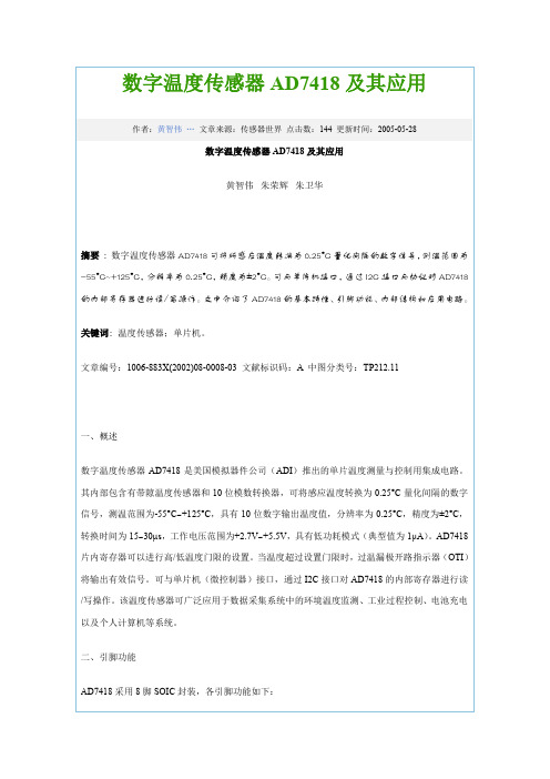
表1温度与输出数据的关系
温度(>°C)
数字输出
–125
–100
–75
–50
–25
–0.25
0
+0.25
+10
+25
+50Leabharlann +75+100
+125
引脚7:VDD,正电源端,2.7V5.5V。
引脚8:/CONVST,逻辑输入信号,转换启动信号。
三、芯片内部结构
AD7418的内部结构框图如图1所示。芯片内包含有温度传感器、基准电压源、10位模数转换器、控制逻辑电路、I2接口电路,温度值寄存器、TOTI温度点寄存器、THYST温度点寄存器、ADC寄存器、配置寄存器1和配置寄存器2、地址指示器寄存器等电路。
1
TOTI寄存器
1
0
0
ADC寄存器
1
0
1
配置寄存器2(读/写)
温度数值寄存器(地址00H)是一个16位的只读寄存器,数据位D15D6用来储存从ADC读出的10位数据,数据位D5D0未使用。
配置寄存器1(地址01H)是一个8位的读/写寄存器。数据位D7D5为通道选择,D7D6D5=000时,选择温度传感器;D7D6D5=100时,选择模拟通道AIN。D4、D3用于设置故障排队长度,以防止测温系统在受到干扰时错误地触发过温指示器(OTI),故障排队长度可分别设置为1、2、4和6次。D2用于设置OTI的输出极性,0表示低电平输出,1表示高电平输出;D1用于设置OTI的工作方式,0表示采用比较方式工作,1表示采用中断方式工作。D0用于设置工作方式,0表示采用自动测温方式,1表示采用低功耗方式。
多功能译码器

课程名称多功能译码器摘要-------------------------------3绪论-------------------------------4工作原理及原---------------------------5方案框图-------------------------------6电路设计余3码转化为格雷码------------------------ 68421BCD码转化为格雷码------------------------------98421码转化为余3码------------------------------------12实验操作图-----------------------------18结论 ------------------------------19 深得体会 ------------------------------20摘要随着电子科学技术日新月异的发展,译码器在我们的生活中广泛应用,它属于组合逻辑电路,它的逻辑功能是将二进制代码按照其编码时的原意译成对应的输出高、低电平相号,又叫解码器。
在数字电子技术中,它具有非常重要的地位,应用也很广泛。
它除了常为其它集成电路长生片选信号之外,还可以作为数据分配器、函数发生器用,而且在组合逻辑电路设计中它可以代替繁多的逻辑门,简化设计电路。
绪论利用多功能译码器可以在很多方面都起着重要作用。
更为显然的是,利用它进行通信可以大大提高信道利用率、缩短信息传输时间、降低传输成本,系统运用组合逻辑电路,采用数据结构知识实现,完成系统的设计、编码和调试。
多功能译码器1、工作原理以及原件:原件:11、08、32、04芯片工作原理:根据所学数电知识,运用组合电路原理,利用与门、或门、非门等门电路实现。
代码简介:8421BCD码:二进制编码的十进制数,简称BCD码(Binarycoded Decimal). 这种方法是用4位二进制码的组合代表十进制数的0,1,2,3,4,5,6 ,7,8,9 十个数符。
- 1、下载文档前请自行甄别文档内容的完整性,平台不提供额外的编辑、内容补充、找答案等附加服务。
- 2、"仅部分预览"的文档,不可在线预览部分如存在完整性等问题,可反馈申请退款(可完整预览的文档不适用该条件!)。
- 3、如文档侵犯您的权益,请联系客服反馈,我们会尽快为您处理(人工客服工作时间:9:00-18:30)。
For price, delivery, and to place orders,please contact Maxim Distribution at 1-888-629-4642,or visit Maxim’s website at .General DescriptionThe MAX7418–MAX7425 5th-order, low-pass, switched-capacitor filters (SCFs) operate from a single +5V (MAX7418–MAX7421) or +3V (MAX7422–MAX7425)supply. These devices draw only 3mA of supply current and allow corner frequencies from 1Hz to 45kHz, mak-ing them ideal for low-power post-DAC filtering and anti-aliasing applications. They feature a shutdown mode that reduces supply current to 0.2µA.Two clocking options are available: self-clocking (through the use of an external capacitor), or external clocking for tighter corner-frequency control. An offset adjust pin allows for adjustment of the DC output level.The MAX7418/MAX7422 deliver 53dB of stopband rejection and a sharp rolloff with a 1.6 transition ratio.The MAX7421/MAX7425 achieve a sharper rolloff with a 1.25 transition ratio while still providing 37dB of stop-band rejection. The MAX7419/MAX7423 Bessel filters provide low overshoot and fast settling, and the MAX7420/MAX7424 Butterworth filters provide a maxi-mally flat passband response. Their fixed response sim-plifies the design task of selecting a clock frequency.ApplicationsADC Anti-Aliasing CT2 Base Stations DAC PostfilteringSpeech ProcessingFeatureso 5th-Order, Lowpass FiltersElliptic Response (MAX7418/MAX7421/ MAX7422/MAX7425)Bessel Response (MAX7419/MAX7423)Butterworth Response (MAX7420/MAX7424)o Clock-Turnable Corner Frequency (1Hz to 45kHz)o Single-Supply Operation+5V (MAX7418–MAX7421)+3V (MAX7422–MAX7425)o Low Power3mA (Operating Mode)0.2µA (Shutdown Mode)o Available in 8-Pin µMAX Package o Low Output Offset: ±4mVMAX7418–MAX74255th-Order, Lowpass,Switched-Capacitor Filters________________________________________________________________Maxim Integrated Products1Typical Operating Circuit19-1821; Rev 0; 11/00Pin ConfigurationOrdering InformationSelector GuideSelector Guide continued at end of data sheet.Ordering Information continued at end of data sheet.M A X 7418–M A X 74255th-Order, Lowpass,Switched-Capacitor Filters 2_______________________________________________________________________________________ABSOLUTE MAXIMUM RATINGSELECTRICAL CHARACTERISTICS —MAX7418–MAX7421(V DD = +5V, filter output measured at OUT, 10k Ω|| 50pF load to GND at OUT, OS = COM, 0.1µF capacitor from COM to GND,SHDN = V DD , f CLK = 2.2MHz, T A = T MIN to T MAX , unless otherwise noted. Typical values are at T A = +25°C.)Stresses beyond those listed under “Absolute Maximum Ratings” may cause permanent damage to the device. These are stress ratings only, and functional operation of the device at these or any other conditions beyond those indicated in the operational sections of the specifications is not implied. Exposure to absolute maximum rating conditions for extended periods may affect device reliability.V DD to GND..............................................................-0.3V to +6V IN, OUT, COM, OS, CLK, SHDN ................-0.3V to (V DD + 0.3V)OUT Short-Circuit Duration.......................................................1s Continuous Power Dissipation (T A = +70°C)8-Pin µMAX (derate 4.1mW/°C above +70°C).............330mWOperating Temperature RangesMAX74 _ _C_A ...................................................0°C to +70°C MAX74 _ _E_A ................................................-40°C to +85°C Junction Temperature......................................................+150°C Storage Temperature Range.............................-65°C to +160°C Lead Temperature (soldering, 10s).................................+300°CMAX7418–MAX74255th-Order, Lowpass,_______________________________________________________________________________________3Switched-Capacitor FiltersELECTRICAL CHARACTERISTICS —MAX7418–MAX7421 (continued)(V DD = +5V, filter output measured at OUT, 10k Ω|| 50pF load to GND at OUT, OS = COM, 0.1µF capacitor from COM to GND,SHDN = V DD , f CLK = 2.2MHz, T A = T MIN to T MAX , unless otherwise noted. Typical values are at T A = +25°C.)ELECTRICAL CHARACTERISTICS —MAX7422–MAX7425(V DD = +3V, filter output measured at OUT pin, 10k Ω|| 50pF load to GND at OUT, OS = COM, 0.1µF capacitor from COM to GND,SHDN = V DD , f CLK = 2.2MHz, T A = T MIN to T MAX , unless otherwise noted. Typical values are at T A = +25°C.)M A X 7418–M A X 74255th-Order, Lowpass,Switched-Capacitor Filters 4_______________________________________________________________________________________FILTER CHARACTERISTICS(V DD = +5V for MAX7418–MAX7421, V DD = +3V for MAX7422–MAX7425 filter output measured at OUT, 10k Ω||50pF load to GND at OUT, SHDN = V DD , f CLK = 2.2MHz, T A = T MIN to T MAX ,unless otherwise noted.)ELECTRICAL CHARACTERISTICS —MAX7422–MAX7425 (continued)(V DD = +3V, filter output measured at OUT pin, 10k Ω|| 50pF load to GND at OUT, OS = COM, 0.1µF capacitor from COM to GND,SHDN = V DD , f CLK = 2.2MHz, T A = T MIN to T MAX , unless otherwise noted. Typical values are at T A = +25°C.)MAX7418–MAX74255th-Order, Lowpass,Switched-Capacitor Filters_______________________________________________________________________________________5Note 1:The maximum f C is defined as the clock frequency f CLK = 100 x f C at which the peak S / (THD+N) drops to 68dB with asinusoidal input at 0.2f C . Maximum f C increases as V IN signal amplitude decreases.Note 2:DC insertion gain is defined as ∆V OUT / ∆V IN .Note 3:MAX7418/MAX7421/MAX7422/MAX7425: f OSC (kHz) ≅ 87x103/ C OSC (pF).MAX7419/MAX7420/MAX7423/MAX7424: f OSC (kHz) ≅ 110x103/ C OSC (pF).Note 4:PSRR is the change in output voltage from a V DD of 4.5V and a V DD of 5.5V.FILTER CHARACTERISTICS(V DD = +5V for MAX7418–MAX7421, V DD = +3V for MAX7422–MAX7425 filter output measured at OUT, 10k Ω||50pF load to GND at OUT, SHDN = V DD , f CLK = 2.2MHz, T A = T MIN to T MAX ,unless otherwise noted.)__________________________________________Typical Operating Characteristics(V DD = +5V for MAX7418–MAX7421, V DD = +3V for MAX7422–MAX7425, f CLK = 2.2MHz, SHDN = V DD , V COM = V OS = V DD / 2, T A = +25°C, unless otherwise noted.)-90-60-70-80-50-40-30-20-1001040206080100MAX7418/MAX7422FREQUENCY RESPONSE (ELLIPTIC, r = 1.6)M A X 7418 t o c 01INPUT FREQUENCY (kHz)G A I N (d B )-60-40-50-20-300-1010040206080100MAX7419/MAX7423FREQUENCY RESPONSE (BESSEL)INPUT FREQUENCY (kHz)G A I N (d B )-80-60-70-30-40-500-10-2010040206080100MAX7420/MAX7424FREQUENCY RESPONSE (BUTTERWORTH)INPUT FREQUENCY (kHz)G A I N (d B )____________________________Typical Operating Characteristics (continued)(V DD = +5V for MAX7418–MAX7421, V DD = +3V for MAX7422–MAX7425, f CLK = 2.2MHz, SHDN = V DD , V COM = V OS = V DD / 2, T A = +25°C, unless otherwise noted.M A X 7418–M A X 74255th-Order, Lowpass,Switched-Capacitor Filters 6_______________________________________________________________________________________-90-60-70-80-50-40-30-20-10010040206080100MAX7421/MAX7425FREQUENCY RESPONSE (ELLIPTIC, r = 1.25)INPUT FREQUENCY (kHz)G A I N (d B)-4.0-3.0-3.5-1.5-2.0-2.50-0.5-1.00.59.04.513.518.022.5MAX7420/MAX7424PASSBAND FREQUENCY RESPONSEINPUT FREQUENCY (kHz)G A I N (d B)-1.0-0.6-0.8-0.2-0.40.200.409.04.513.518.022.5MAX7418/MAX7422PASSBAND FREQUENCY RESPONSE(ELLIPTIC, r = 1.6)INPUT FREQUENCY (kHz)G A I N (d B)-4.0-3.0-3.5-1.5-2.0-2.50-0.5-1.00.509.04.513.518.022.5MAX7419/MAX7423PASSBAND FREQUENCY RESPONSE(BESSEL)INPUT FREQUENCY (kHz)G A I N (d B )-1.0-0.6-0.8-0.2-0.40.200.409.04.513.518.022.5MAX7421/MAX7425PASSBAND FREQUENCY RESPONSE(ELLIPTIC, r = 1.25)INPUT FREQUENCY (kHz)G A I N (d B )-450-350-400-200-250-300-50-100-15000812416202428MAX7418/MAX7422PHASE RESPONSE (ELLIPTIC, r = 1.6)INPUT FREQUENCY (kHz)P H A S E S H I F T (D E G R E E S )M A X 7418 t o c 09-250-200-100-150-5000841216202428MAX7419/MAX7423PHASE RESPONSE (BESSEL)M A X 7418 t o c 10INPUT FREQUENCY (kHz)P H A S E S H I F T (D E G R E E S )-350-250-300-150-200-50-10000812416202428MAX7420/MAX7424PHASE RESPONSE (BUTTERWORTH)M A X 7418 t o c 11INPUT FREQUENCY (kHz)P H A S E S H I F T (D E G R E E S )-450-350-400-200-250-300-50-100-1500812416202428MAX7424/MAX7425PHASE RESPONSE (ELLIPTIC, r = 1.25)M A X 7418 t o c 12INPUT FREQUENCY (kHz)P H A S E S H I F T (D E G R E E S )____________________________Typical Operating Characteristics (continued)(V DD = +5V for MAX7418–MAX7421, V DD = +3V for MAX7422–MAX7425, f CLK = 2.2MHz, SHDN = V DD , V COM = V OS = V DD / 2, T A = +25°C, unless otherwise noted.MAX7418–MAX74255th-Order, Lowpass,Switched-Capacitor Filters_______________________________________________________________________________________7-90-70-80-40-50-60-10-20-300021345MAX7418THD + NOISE vs. INPUT SIGNAL AMPLITUDE(ELLIPTIC, r = 1.6)AMPLITUDE (Vp-p)T H D + N (d B )-90-70-80-40-50-60-10-20-300021345MAX7421THD + NOISE vs. INPUT SIGNAL AMPLITUDE(ELLIPTIC, r = 1.25)AMPLITUDE (Vp-p)T H D + N (d B )-90-70-80-40-50-60-10-20-300021345MAX7419THD + NOISE vs. INPUT SIGNAL AMPLITUDE(BESSEL)AMPLITUDE (Vp-p)T H D + N (d B )-90-70-80-40-50-60-10-20-30021345MAX7420THD + NOISE vs. INPUT SIGNAL AMPLITUDE(BUTTERWORTH)AMPLITUDE (Vp-p)T H D + N (d B )-90-70-80-40-50-60-10-20-30001.00.51.52.0 2.53.0MAX7422THD + NOISE vs. INPUT SIGNAL AMPLITUDE(ELLIPTIC, r = 1.6)AMPLITUDE (Vp-p)T H D + N (d B)-90-70-80-40-50-60-10-20-3001.00.51.52.02.53.0MAX7423THD + NOISE vs. INPUT SIGNAL AMPLITUDE(BESSEL)AMPLITUDE (Vp-p)T H D + N (d B)-90-70-80-40-50-60-30-20-10000.51.01.52.02.53.0MAX7424THD + NOISE vs. INPUT SIGNAL AMPLITUDE(BUTTERWORTH)AMPLITUDE (Vp-p)T H D + N (d B )-90-70-80-40-50-60-30-20-10000.51.01.52.02.53.0MAX7425THD + NOISE vs. INPUT SIGNAL AMPLITUDE(ELLIPTIC, r = 1.25)AMPLITUDE (Vp-p)T H D + N (d B )02000100040003000600050007000INTERNAL OSCILLATOR FREQUENCY vs. SMALL CAPACITANCE (pF)CAPACITANCE ( pF)O S C I L L A T O R F R E Q U E N C Y (k H z )110100100010000____________________________Typical Operating Characteristics (continued)(V DD = +5V for MAX7418–MAX7421, V DD = +3V for MAX7422–MAX7425, f CLK = 2.2MHz, SHDN = V DD , V COM = V OS = V DD / 2, T A = +25°C, unless otherwise noted.M A X 7418–M A X 74255th-Order, Lowpass,Switched-Capacitor Filters 8_______________________________________________________________________________________0214356101001000INTERNAL OSCILLATOR FREQUENCY vs. LARGE CAPACITANCE (nF)CAPACITANCE (nF)O S C I L L A T O R F R E Q U E N C Y (H z )2.32.52.92.73.13.32.53.53.04.04.55.05.5ELLIPTIC SUPPLY CURRENT vs. SUPPLY VOLTAGEM A X 7418 t o c 25SUPPLY VOLTAGE (V)S U P P L Y C U R R E N T (µA )84.085.084.586.085.586.587.02.53.54.03.04.55.05.5ELLIPTIC INTERNAL OSCILLATOR FREQUENCY vs. SUPPLY VOLTAGESUPPLY VOLTAGE (V)O S C I L L A T O R F R E Q U E N C Y (k H z )84.085.084.586.085.586.587.0-4010-15356085ELLIPTIC INTERNAL OSCILLATOR FREQUENCY vs. TEMPERATURETEMPERATURE (°C)O S C I L L A T O R F R E Q U E N C Y (k H z) 2.52.62.82.72.93.0-4010-15356085ELLIPTIC SUPPLY CURRENTvs. TEMPERATURETEMPERATURE (°C)S U P P L Y C U R R E N T (m A )MAX7418–MAX74255th-Order, Lowpass,Switched-Capacitor Filters_______________________________________________________________________________________9Pin Description_______________Detailed DescriptionThe MAX7418/MAX7421/MAX7422/MAX7425 elliptic lowpass filters provide sharp rolloff with good stopband rejection. The MAX7419/MAX7423 Bessel filters provide low overshoot and fast settling responses, and the MAX7420/MAX7424 Butterworth filters provide a maxi-mally flat passband response. All parts operate with a 100:1 clock-to-corner frequency ratio.Most switch capacitor filters (SCFs) are designed with biquadratic sections. Each section implements two pole-zero pairs, and the sections can be cascaded toproduce higher order filters. The advantage to this approach is ease of design. H owever, this type of design is highly sensitive to component variations if any section’s Q is high. The MAX7418–MAX7425 use an alternative approach, which is to emulate a passive net-work using switched-capacitor integrators with sum-ming and scaling. The passive network may be synthesized using CAD programs, or may be found in many filter books. Figure 1 shows a basic 5th-order lad-der filter structure.Typical Operating Characteristics (continued)(V DD = +5V for MAX7418–MAX7421, V DD = +3V for MAX7422–MAX7425, f CLK = 2.2MHz, SHDN = V DD , V COM = V OS = V DD / 2, T A = +25°C, unless otherwise noted.0.51.51.02.02.52.53.53.04.04.55.05.5DC OFFSET VOLTAGE vs. SUPPLY VOLTAGEM A X 7418 t o c 28SUPPLY VOLTAGE (V)D C O F F SE T V O L T A G E (m V )01.00.52.01.52.53.0-4010-15356085DC OFFSET VOLTAGE vs. TEMPERATURETEMPERATURE (°C)D C O F F SE T V O L T A G E (m V )Filter OutputOUT 5Offset Adjust Input. To adjust output offset, connect OS to an external supply through a resistive voltage-divider (Figure 4). Connect OS to COM if no offset adjustment is needed. See the Offset and Common-Mode Input Adjustment section.OS 6Shutdown Input. Drive low to enable shutdown mode; drive high or connect to V DD for normal operation. SHDN 7Clock Input. Connect an external capacitor (C OSC ) from CLK to ground. To override the internal oscillator,connect CLK to an external clock: f C = f CLK /100.CLK8Positive Supply Input: +5V for MAX7418–MAX7421, +3V for MAX7422–MAX7425. Bypass V DD to GND with a 0.1µF capacitor.V DD 4GroundGND 3PIN Filter Input IN 2Common Input Pin. Biased internally at midsupply. Bypass COM externally to GND with a 0.1µF capacitor.To override internal biasing, drive COM with an external 1FUNCTIONNAMEM A X 7418–M A X 74255th-Order, Lowpass,Switched-Capacitor Filters 10______________________________________________________________________________________An SCF that emulates a passive ladder filter retains many of the same advantages. The component sensi-tivity of a passive ladder filter is low when compared to a cascaded biquadratic design because each compo-nent affects the entire filter shape rather than a single pole-zero pair. In other words, a mismatched compo-nent in a biquadratic design has a concentrated error on its respective poles, while the same mismatch in a ladder filter design spreads its error over all poles.Elliptic CharacteristicsLowpass elliptic filters such as the MAX7418/MAX7421/MAX7422/MAX7425 provide the steepest possible rolloff with frequency of the four most common filter types (Butterworth, Bessel, Chebyshev, and elliptic).The high-Q value of the poles near the passband edge combined with the stopband zeros allow for the sharp attenuation characteristic of elliptic filters, making these devices ideal for anti-aliasing and post-DAC filtering in single-supply systems (see Anti-Aliasing and Post-DAC Filtering ).In the frequency domain, the first transmission zero causes the filter’s amplitude to drop to a minimum level (Figure 2). Beyond this zero, the response rises as the frequency increases until the next transmission zero.The stopband begins at the stopband frequency, f S . At frequencies above f S , the filter’s gain does not exceed the gain at f S . The corner frequency, f C , is defined as the point at which the filter output attenuation falls just below the passband ripple. The transition ratio (r) is defined as the ratio of the stopband frequency to the corner frequency:r = f S / f CThe MAX7418/MAX7422 have a transition ratio of 1.6and typically 53dB of stopband rejection. The MAX7421/MAX7425 have a transition ratio of 1.25 (pro-viding a steeper rolloff) and typically 37dB of stopband rejection.Bessel CharacteristicsLowpass Bessel filters such as the MAX7419/MAX7423delay all frequency components equally, preserving the line up shape of step inputs (subject to the attenuation of the higher frequencies). Bessel filters settle quickly—an important characteristic in applications that use a multiplexer (mux) to select an input signal for an ana-log-to-digital converter (ADC). An anti-aliasing filter placed between the mux and the ADC must settle quickly after a new channel is selected.Butterworth CharacteristicsLowpass Butterworth filters such as the MAX7420/MAX7424 provide a maximally flat passband response,making them ideal for instrumentation applications that require minimum deviation from the DC gain throughout the passband.The difference between Bessel and Butterworth filters can be observed when a 1kHz square wave is applied to the filter input (Figure 3, trace A). With the filter cutoff frequencies set at 5kHz, trace B shows the Bessel filter response and trace C shows the Butterworth filter response.Clock SignalExternal ClockThese SCFs are designed for use with external clocks that have a 40% to 60% duty cycle. When using an external clock, drive the CLK pin with a CMOS gate powered from 0 to V DD . Varying the rate of the external clock adjusts the corner frequency of the filter:Figure 1. 5th-Order Ladder Filter NetworkFigure 2. Elliptic Filter ResponseMAX7418–MAX74255th-Order, Lowpass, Switched-Capacitor Filters______________________________________________________________________________________11Internal ClockWhen using the internal oscillator, the capacitance (C OSC ) on CLK determines the oscillator frequency:wherek = 87 x 103 for theMAX7418/MAX7421/MAX7422/MAX7425 andk = 110 x 103for theMAX7419/MAX7420/MAX7423/ MAX7424.Since C OSC is in the low picofarads, minimize the stray capacitance at CLK so that it does not affect the inter-nal oscillator frequency. Varying the rate of the internal oscillator adjusts the filter’s corner frequency by a100:1 clock-to-corner frequency ratio. For example, an internal oscillator frequency of 2.2MHz produces a nominal corner frequency of 2.2kHz.Input Impedance vs. Clock FrequenciesThe MAX7418–MAX7425s’ input impedance is effective as a switched-capacitor resistor and is inversely propor-tional to frequency. The input impedance values deter-mined by the equation represents the average input impedance, since the input current is not continuous.As a rule, use a driver with an output resistance less than 10% of the filter’s input impedance.Estimate the input impedance of the filter by using the following formula:where f CLK = clock frequency and C IN = 1pF.Low-Power Shutdown ModeThe MAX7418–MAX7425have a shutdown mode that isactivated by driving SHDN low. In shutdown mode, the filter supply current reduces to 0.2µA, and the output of the filter becomes high impedance. For normal opera-tion, drive SHDN high or connect to V DD .Applications InformationOffset (OS) and Common-Mode (COM)Input AdjustmentCOM sets the common-mode input voltage and is biased at midsupply with an internal resistor-divider. If the application does not require offset adjustment, con-nect OS to COM. For applications in which offset adjustment is required, apply an external bias voltage through a resistor-divider network to OS, as shown in Figure 4. For applications that require DC level shifting,adjust OS with respect to COM. (Note:Do not leave OS unconnected.) The output voltage is represented bywhere (V IN - V COM ) is lowpass filtered by the SCF and OS is added at the output stage. See the Electrical Characteristics table for the input voltage range of COMf OSC (kHz) kC OSC (pF)=Figure 4. Offset Adjustment CircuitA: 1kHz INPUT SIGNALB: MAX7419 BESSEL FILTER RESPONSE; f C = 5kHzC: MAX7420 BUTTERWORTH FILTER RESPONSE; f C = 5kHz200µs/divFigure 3. Bessel vs. Butterworth Filter ResponseM A X 7418–M A X 74255th-Order, Lowpass,Switched-Capacitor Filtersand OS. Changing the voltage on COM or OS signifi-cantly from midsupply reduces the dynamic range.Power SuppliesThe MAX7418–MAX7421 operate from a single +5V supply and the MAX7422–MAX7425 operate from a sin-gle +3V supply. Bypass V DD to GND with a 0.1µF capacitor. If dual supplies are required, connect COM to the system ground and GND to the negative supply.Figure 5 shows an example of dual-supply operation.Single-supply and dual-supply performance are equiv-alent. For either single-supply or dual-supply operation,drive CLK and SHDN from GND (V- in dual supply operation) to V DD . Use the MAX7418–MAX7421 for ±2.5, and use the MAX7422–MAX7425 for ±1.5V. For ±5V dual-supply applications, refer to the MAX291/MAX292/MAX295/MAX296 and MAX293/MAX294/MAX297 data sheets.Input Signal Amplitude RangeThe optimal input signal range is determined by observ-ing the voltage level at which the signal-to-noise plus distortion (SINAD) ratio is maximized for a given corner frequency. The Typic al Operating Charac teristic s show the THD + Noise response as the input signal’s peak-to-peak amplitude is varied.Anti-Aliasing and Post-DAC FilteringWhen using the MAX7418–MAX7425 for anti-aliasing or post-DAC filtering, synchronize the DAC (or ADC) and the filter clocks. If the clocks are not synchronized, beat frequencies may alias into the desired passband.Harmonic DistortionHarmonic distortion arises from nonlinearities within the filter. These nonlinearities generate harmonics when a pure sine wave is applied to the filter input. Tables 1, 2,and 3 list typical harmonic distortion values with a 10k Ωload at T A = +25°C.Table 1. MAX7418/MAX7421/MAX7422/MAX7425 Typical Harmonic DistortionFigure 5. Dual-Supply OperationMAX7418–MAX74255th-Order, Lowpass,Switched-Capacitor Filters______________________________________________________________________________________13Chip InformationTRANSISTOR COUNT:1457PROCESS: BiCMOSOrdering Information (continued)Selector Guide (continued)M A X 7418–M A X 74255th-Order, Lowpass,Switched-Capacitor Filters Maxim c annot assume responsibility for use of any c irc uitry other than c irc uitry entirely embodied in a Maxim produc t. No c irc uit patent lic enses are implied. Maxim reserves the right to change the circuitry and specifications without notice at any time.14____________________Maxim Integrated Products, 120 San Gabriel Drive, Sunnyvale, CA 94086 408-737-7600© 2000 Maxim Integrated ProductsPrinted USAis a registered trademark of Maxim Integrated Products.________________________________________________________Package Information。