L7386A中文资料
HT7136A中文资料
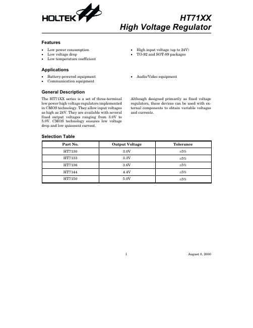
HT71XXHigh Voltage RegulatorSelection TablePart No.Output VoltageToleranceHT7130 3.0V ±5%HT7133 3.3V ±5%HT7136 3.6V ±5%HT7144 4.4V ±5%HT71505.0V±5%1August 8,2000Features·Low power consumption ·Low voltage drop·Low temperature coefficient·High input voltage (up to 24V)·TO-92and SOT-89packagesApplications·Battery-powered equipment ·Communication equipment·Audio/Video equipmentGeneral DescriptionThe HT71XX series is a set of three-terminal low power high voltage regulators implemented in CMOS technology.They allow input voltages as high as 24V.They are available with several fixed output voltages ranging from 3.0V to 5.0V.CMOS technology ensures low voltage drop and low quiescent current.Although designed primarily as fixed voltage regulators,these devices can be used with ex-ternal components to obtainvariable voltages and currents.Block DiagramPin AssignmentPad Assignment Pad CoordinatesUnit:m m Pad No.X Y 1-480.00-451.50287.50-444.503482.00-444.50Chip size:1374´1294(m m)2*The IC substrate should be connected to VDD in the PCB layout artwork.2August 8,2000Absolute Maximum RatingsSupply Voltage..............................-0.3V to28V Storage Temperature................-50°C to125°C Power Consumption.............................200mW Operating Temperature.................0°C to70°CNote:These are stress ratings only.Stresses exceeding the range specified under Absolute Maxi-mum Ratings may cause substantial damage to the device.Functional operation of this de-vice at other conditions beyond those listed in the specification is not implied and prolonged exposure to extreme conditions may affect device reliability.Electrical CharacteristicsHT7130,+3.0V output typeHT7133,+3.3V output type Ta=25°C3August8,2000HT7144,+4.4V output type Ta=25°C4August8,2000Application CircuitsBasic circuits5August8,2000High output current positive voltage regulatorShort-Circuit protection by Tr1Circuit for increasing output voltageV V (1+R2R1)I R2OUT XX SS =+HT71XX6August 8,2000Circuit for increasing output voltageV OUT=V XX+V D1 Constant current regulatorI VR IOUTXXA SS=+Dual supply7August8,20008August 8,2000Copyright Ó2000by HOLTEK SEMICONDUCTOR INC.The information appearing in this Data Sheet is believed to be accurate at the time of publication.However,Holtek assumes no responsibility arising from the use of the specifications described.The applications mentioned herein are used solely for the purpose of illustration and Holtek makes no warranty or representation that such applications will be suitable without further modification,nor recommends the use of its products for application that may pres-ent a risk to human life due to malfunction or otherwise.Holtek reserves the right to alter its products without prior notification.For the most up-to-date information,please visit our web site at .Holtek Semiconductor Inc.(Headquarters)No.3Creation Rd.II,Science-based Industrial Park,Hsinchu,Taiwan,R.O.C.Tel:886-3-563-1999Fax:886-3-563-1189Holtek Semiconductor Inc.(Taipei Office)5F,No.576,Sec.7Chung Hsiao E.Rd.,Taipei,Taiwan,R.O.C.Tel:886-2-2782-9635Fax:886-2-2782-9636Fax:886-2-2782-7128(International sales hotline)Holtek Semiconductor (Hong Kong)Ltd.RM.711,Tower 2,Cheung Sha Wan Plaza,833Cheung Sha Wan Rd.,Kowloon,Hong Kong Tel:852-2-745-8288Fax:852-2-742-8657。
ST L7800AB AC SERIES 说明书

现货库存、技术资料、百科信息、热点资讯,精彩尽在鼎好!L7800AB/ACSERIESPRECISION 1A REGULATORS®November 1999s OUTPUT CURRENT IN EXCESS OF 1AsOUTPUT VOLTAGESOF 5;6;8;9;12;15;18;20;24Vs THERMAL OVERLOAD PROTECTIONs OUTPUT TRANSITION SOA PROTECTION s 2%OUTPUT VOLTAGE TOLERANCE sGUARANTEED IN EXTENDED TEMPERATURE RANGEDESCRIPTIONThe L7800A series of three-terminal positive regulators is available in TO-220and D 2PAK packages and several fixed output voltages,making it useful in a wide range of applications.These regulators can provide local on-card regulation,eliminating the distribution problems associated with single point regulation.Each type employs internal current limiting,thermal shut-down and safe area protection,making it essentially indestructible.If adequate heat sinking is provided,they can deliver over 1A output current.Although designed primarily as fixed voltage regulators,these devices can be used with external components to obtain adjustable voltages and currents.TO-220D 2PAKBLOCK DIAGRAM1/17CONNECTION DIAGRAM AND ORDERING NUMBERS (top view)TO-220D 2PAKTHERMAL DATASymbolParameterD 2PAK TO-220UnitR thj-ca se R thj-amb Thermal Resistance Junction-case Max Thermal Resistance Junction-ambient Max362.5350o C/W oC/WTypeTO-220D 2PAK (*)Output VoltageL7805AB L7805AC L7806AB L7806AC L7808AB L7808AC L7809AB L7809AC L7812AB L7812AC L7815AB L7815AC L7818AB L7818AC L7820AB L7820AC L7824AB L7824ACL7805ABV L7805ACV L7806ABV L7806ACV L7808ABV L7808ACV L7809ABV L7809ACV L7812ABV L7812ACV L7815ABV L7815ACV L7818ABV L7818ACV L7820ABV L7820ACV L7824ABV L7824ACVL7805ABD2T L7805ACD2T L7806ABD2T L7806ACD2T L7808ABD2T L7808ACD2T L7809ABD2T L7809ACD2T L7812ABD2T L7812ACD2T L7815ABD2T L7815ACD2T5V 5V 6V 6V 8V 8V 9V 9V 12V 12V 15V 15V 18V 18V 24V 24V(*)AVAILABLE IN TAPE AND REEL WITH ”-TR”SUFFIXABSOLUTE MAXIMUM RATINGSSymbol ParameterValue Unit V i DC Input Voltage (for V O =5to 18V)(for V O =20,24V)3540V VI o Output Current Internally limited P tot Power DissipationInternally limitedT op Operating Junction Temperature Range (for L7800AC )(for L7800AB )0to 150-40to 125o C o C T st gStorage Temperature Range-65to 150oCL7800AB/AC2/17L7800AB/AC APPLICATION CIRCUITSCHEMATIC DIAGRAM3/17TEST CIRCUITSFigure3:Ripple Rejection.Figure2:Load Regulation.Figure1:DC Parameter L7800AB/AC4/17*Load and line regulation are specified at constant junction temperature.Changes in V o due to heating effects must be taken into account separately.Pulse testing with low duty cycle is used.ELECTRICAL CHARACTERISTICS FOR L7805A (V i =10V,I o =1A,T j =0to 125o C (L7805AC),T j =-40to 125o C (L7805AB)unless otherwise specified)Symbol ParameterTest ConditionsMin.Typ.Max.Unit V o Output Voltage T j =25o C 4.95 5.1V V o Output Voltage I o =5mA to 1A P o ≤15W V i =7.5to 20V 4.85 5.2V ∆V o *Line RegulationV i =7.5to 25V I o =500mA V i =8to 12V V i =8to 12V T j =25o C V i =7.3to 20VT j =25o C710275052550mV mV mV mV ∆V o *Load RegulationI o =5mA to 1AI o =5mA to 1.5A T j =25o C I o =250to 750mA 2530810010050mV mV mV I d Quiescent Current T j =25oC4.366mA ∆I dQuiescent Current ChangeV i =8to 25V I o =500mAV i =7.5to 20VT j =25o C I o =5mA to 1A 0.80.80.5mA mA mA SVR Supply Voltage Rejection V i =8to 18V f =120HzI o =500mA 68dB V d Dropout Voltage I o =1AT j =25o C2V e N Output Noise Voltage B =10Hz to 100KHz T j =25oC10µV/V o R o Output Resistance f =1KHz 17m ΩI s c Short Circuit Current V i =35V T amb =25o C0.2A I scp Short Circuit Peack Current T j =25o C2.2A ∆V o∆TOutput Voltage Drift-1.1mV/o CL7800AB/AC5/17ELECTRICAL CHARACTERISTICS FOR L7806A(V i=11V,I o=1A,T j=0to125o C(L7806AC),T j=-40to125o C(L7806AB)unless otherwise specified)Symbol Parameter Test Conditions Min.Typ.Max.Unit V o Output Voltage T j=25o C 5.886 6.12V V o Output Voltage I o=5mA to1A P o≤15WV i=8.6to21V5.7666.24V∆V o*Line Regulation V i=8.6to25V I o=500mAV i=9to13VV i=9to13V T j=25o CV i=8.3to21V T j=25o C9113960603060mVmVmVmV∆V o*Load Regulation I o=5mA to1AI o=5mA to1.5A T j=25o CI o=250to750mA 25301010010050mVmVmVI d Quiescent Current T j=25o C 4.366mA∆I d Quiescent Current Change V i=9to25V I o=500mAV i=8.6to21V T j=25o CI o=5mA to1A 0.80.80.5mAmAmASVR Supply Voltage Rejection V i=9to19V f=120HzI o=500mA65dB V d Dropout Voltage I o=1A T j=25o C2Ve N Output Noise Voltage B=10Hz to100KHz T j=25o C10µV/V oR o Output Resistance f=1KHz17mΩI s c Short Circuit Current V i=35V T amb=25o C0.2AI scp Short Circuit Peack Current T j=25o C 2.2A∆V o∆TOutput Voltage Drift-0.8mV/o C*Load and line regulation are specified at constant junction temperature.Changes in V o due to heating effects must be taken into account separately.Pulse testing with low duty cycle is used.L7800AB/AC6/17ELECTRICAL CHARACTERISTICS FOR L7808A(V i=14V,I o=1A,T j=0to125o C(L7808AC),T j=-40to125o C(L7808AB)unless otherwise specified)Symbol Parameter Test Conditions Min.Typ.Max.Unit V o Output Voltage T j=25o C7.8488.16V V o Output Voltage I o=5mA to1A P o≤15WV i=10.6to23V7.788.3V∆V o*Line Regulation V i=10.6to25V I o=500mAV i=11to17VV i=11to17V T j=25o CV i=10.4to23V T j=25o C 121551280804080mVmVmVmV∆V o*Load Regulation I o=5mA to1AI o=5mA to1.5A T j=25o CI o=250to750mA 25301010010050mVmVmVI d Quiescent Current T j=25o C 4.366mA∆I d Quiescent Current Change V i=11to25V I o=500mAV i=10.6to23V T j=25o CI o=5mA to1A 0.80.80.5mAmAmASVR Supply Voltage Rejection V i=11.5to21.5V f=120HzI o=500mA62dB V d Dropout Voltage I o=1A T j=25o C2Ve N Output Noise Voltage B=10Hz to100KHz T j=25o C10µV/V oR o Output Resistance f=1KHz18mΩI s c Short Circuit Current V i=35V T amb=25o C0.2AI scp Short Circuit Peack Current T j=25o C 2.2A∆V o∆TOutput Voltage Drift-0.8mV/o C*Load and line regulation are specified at constant junction temperature.Changes in V o due to heating effects must be taken into account separately.Pulse testing with low duty cycle is used.L7800AB/AC7/17ELECTRICAL CHARACTERISTICS FOR L7809A(V i=15V,I o=1A,T j=0to125o C(L7809AC),T j=-40to125o C(L7809AB)unless otherwise specified)Symbol Parameter Test Conditions Min.Typ.Max.Unit V o Output Voltage T j=25o C8.8299.18V V o Output Voltage I o=5mA to1A P o≤15WV i=10.6to23V8.6599.35V∆V o*Line Regulation V i=10.6to25V I o=500mAV i=11to17VV i=11to17V T j=25o CV i=10.4to23V T j=25o C 121551290904590mVmVmVmV∆V o*Load Regulation I o=5mA to1AI o=5mA to1.5A T j=25o CI o=250to750mA 25301010010050mVmVmVI d Quiescent Current T j=25o C 4.366mA∆I d Quiescent Current Change V i=11to25V I o=500mAV i=10.6to23V T j=25o CI o=5mA to1A 0.80.80.5mAmAmASVR Supply Voltage Rejection V i=11.5to21.5V f=120HzI o=500mA61dB V d Dropout Voltage I o=1A T j=25o C2Ve N Output Noise Voltage B=10Hz to100KHz T j=25o C10µV/V oR o Output Resistance f=1KHz18mΩI s c Short Circuit Current V i=35V T amb=25o C0.2AI scp Short Circuit Peack Current T j=25o C 2.2A∆V o∆TOutput Voltage Drift-0.8mV/o C*Load and line regulation are specified at constant junction temperature.Changes in V o due to heating effects must be taken into account separately.Pulse testing with low duty cycle is used.L7800AB/AC8/17ELECTRICAL CHARACTERISTICS FOR L7812A(V i=19V,I o=1A,T j=0to125o C(L7812AC),T j=-40to125o C(L7812AB)unless otherwise specified)Symbol Parameter Test Conditions Min.Typ.Max.Unit V o Output Voltage T j=25o C11.751212.25V V o Output Voltage I o=5mA to1A P o≤15WV i=14.8to27V11.51212.5V∆V o*Line Regulation V i=14.8to30V I o=500mAV i=16to22VV i=16to22V T j=25o CV i=14.5to27V T j=25o C 131661312012060120mVmVmVmV∆V o*Load Regulation I o=5mA to1AI o=5mA to1.5A T j=25o CI o=250to750mA 25301010010050mVmVmVI d Quiescent Current T j=25o C 4.466mA∆I d Quiescent Current Change V i=15to30V I o=500mAV i=14.8to27V T j=25o CI o=5mA to1A 0.80.80.5mAmAmASVR Supply Voltage Rejection V i=15to25V f=120HzI o=500mA60dB V d Dropout Voltage I o=1A T j=25o C2Ve N Output Noise Voltage B=10Hz to100KHz T j=25o C10µV/V oR o Output Resistance f=1KHz18mΩI s c Short Circuit Current V i=35V T amb=25o C0.2AI scp Short Circuit Peack Current T j=25o C 2.2A∆V o∆TOutput Voltage Drift-1mV/o C*Load and line regulation are specified at constant junction temperature.Changes in V o due to heating effects must be taken into account separately.Pulse testing with low duty cycle is used.L7800AB/AC9/17ELECTRICAL CHARACTERISTICS FOR L7815A(V i=23V,I o=1A,T j=0to125o C(L7815AC),T j=-40to125o C(L7815AB)unless otherwise specified)Symbol Parameter Test Conditions Min.Typ.Max.Unit V o Output Voltage T j=25o C14.71515.3V V o Output Voltage I o=5mA to1A P o≤15WV i=17.9to30V14.41515.6V∆V o*Line Regulation V i=17.9to30V I o=500mAV i=20to26VV i=20to26V T j=25o CV i=17.5to30V T j=25o C 131661315015075150mVmVmVmV∆V o*Load Regulation I o=5mA to1AI o=5mA to1.5A T j=25o CI o=250to750mA 25301010010050mVmVmVI d Quiescent Current T j=25o C 4.466mA∆I d Quiescent Current Change V i=17.5to30V I o=500mAV i=17.5to30V T j=25o CI o=5mA to1A 0.80.80.5mAmAmASVR Supply Voltage Rejection V i=18.5to28.5V f=120HzI o=500mA58dB V d Dropout Voltage I o=1A T j=25o C2Ve N Output Noise Voltage B=10Hz to100KHz T j=25o C10µV/V oR o Output Resistance f=1KHz19mΩI s c Short Circuit Current V i=35V T amb=25o C0.2AI scp Short Circuit Peack Current T j=25o C 2.2A∆V o∆TOutput Voltage Drift-1mV/o C*Load and line regulation are specified at constant junction temperature.Changes in V o due to heating effects must be taken into account separately.Pulse testing with low duty cycle is used.L7800AB/AC10/17ELECTRICAL CHARACTERISTICS FOR L7818A(V i=27V,I o=1A,T j=0to125o C(L7818AC),T j=-40to125o C(L7818AB)unless otherwise specified)Symbol Parameter Test Conditions Min.Typ.Max.Unit V o Output Voltage T j=25o C17.641818.36V V o Output Voltage I o=5mA to1A P o≤15WV i=21to33V17.31818.7V∆V o*Line Regulation V i=21to33V I o=500mAV i=24to30VV i=24to30V T j=25o CV i=20.6to33V T j=25o C 252810518018090180mVmVmVmV∆V o*Load Regulation I o=5mA to1AI o=5mA to1.5A T j=25o CI o=250to750mA 25301010010050mVmVmVI d Quiescent Current T j=25o C 4.566mA∆I d Quiescent Current Change V i=21to33V I o=500mAV i=21to33V T j=25o CI o=5mA to1A 0.80.80.5mAmAmASVR Supply Voltage Rejection V i=22to32V f=120HzI o=500mA57dB V d Dropout Voltage I o=1A T j=25o C2Ve N Output Noise Voltage B=10Hz to100KHz T j=25o C10µV/V oR o Output Resistance f=1KHz19mΩI s c Short Circuit Current V i=35V T amb=25o C0.2AI scp Short Circuit Peack Current T j=25o C 2.2A∆V o∆TOutput Voltage Drift-1mV/o C*Load and line regulation are specified at constant junction temperature.Changes in V o due to heating effects must be taken into account separately.Pulse testing with low duty cycle is used.11/17ELECTRICAL CHARACTERISTICS FOR L7820A(V i=28V,I o=1A,T j=0to125o C(L7820AC),T j=-40to125o C(L7820AB)unless otherwise specified)Symbol Parameter Test Conditions Min.Typ.Max.Unit V o Output Voltage T j=25o C19.62020.4V V o Output Voltage I o=5mA to1A P o≤15WV i=23to35V19.22020.8V∆V o*Line Regulation V i=23to35V I o=500mAV i=26to32VV i=26to32V T j=25o CV i=23to32V T j=25o C 200200100200mVmVmVmV∆V o*Load Regulation I o=5mA to1AI o=5mA to1.5A T j=25o CI o=250to750mA 25301010010050mVmVmVI d Quiescent Current T j=25o C 4.566mA∆I d Quiescent Current Change V i=23to35V I o=500mAV i=23to35V T j=25o CI o=5mA to1A 0.80.80.5mAmAmASVR Supply Voltage Rejection V i=24to35V f=120HzI o=500mA56dB V d Dropout Voltage I o=1A T j=25o C2Ve N Output Noise Voltage B=10Hz to100KHz T j=25o C10µV/V oR o Output Resistance f=1KHz20mΩI s c Short Circuit Current V i=35V T amb=25o C0.2AI scp Short Circuit Peack Current T j=25o C 2.2A∆V o∆TOutput Voltage Drift-1mV/o C*Load and line regulation are specified at constant junction temperature.Changes in V o due to heating effects must be taken into account separately.Pulse testing with low duty cycle is used.12/17ELECTRICAL CHARACTERISTICS FOR L7824A(V i=33V,I o=1A,T j=0to125o C(L7824AC),T j=-40to125o C(L7824AB)unless otherwise specified)Symbol Parameter Test Conditions Min.Typ.Max.Unit V o Output Voltage T j=25o C23.52424.5V V o Output Voltage I o=5mA to1A P o≤15WV i=27.3to38V232425V∆V o*Line Regulation V i=27to38V I o=500mAV i=30to36VV i=30to36V T j=25o CV i=26.7to38V T j=25o C 31351431240240120240mVmVmVmV∆V o*Load Regulation I o=5mA to1AI o=5mA to1.5A T j=25o CI o=250to750mA 25301010010050mVmVmVI d Quiescent Current T j=25o C 4.666mA∆I d Quiescent Current Change V i=27.3to38V I o=500mAV i=27.3to38V T j=25o CI o=5mA to1A 0.80.80.5mAmAmASVR Supply Voltage Rejection V i=28to38V f=120HzI o=500mA54dB V d Dropout Voltage I o=1A T j=25o C2Ve N Output Noise Voltage B=10Hz to100KHz T j=25o C10µV/V oR o Output Resistance f=1KHz20mΩI s c Short Circuit Current V i=35V T amb=25o C0.2AI scp Short Circuit Peack Current T j=25o C 2.2A∆V o∆TOutput Voltage Drift-1.5mV/o C*Load and line regulation are specified at constant junction temperature.Changes in V o due to heating effects must be taken into account separately.Pulse testing with low duty cycle is used.13/17APPLICATIONS INFORMATIONDESIGN CONSIDERATIONSThe L7800A Series of fixed voltage regulators are designed with Thermal Overload Protection that shuts down the circuit when subjected to an excessive power overload condition,Internal Short-circuit Protection that limits the maximum current the circuit will pass,and Output Transistor Safe-Area Compensation that reduces the output short-circuit current as the voltage across the pass transistor is increased.In many low current applications,compensation capacitors are not required.However,it is recommended that the regulator input be bypassed with a capacitor if the regulator is connected to the power supply filter with long wire lengths,or if the output load capacitance is large.An input bypass capacitor should be selected to provide good high-frequency characteristics to insure stable operation under all load conditions.A 0.33µF or larger tantalum,mylar,or other capacitor having low internal impedance at high frequencies should be chosen.The bypass capacitor should be mounted with the shortest possible leads directly across the regulators input terminals.Normally good construction techniques should be used to minimize ground loops and lead resistance drops since the regulator has no external sense lead.Figure 4:Current Regulator.Figure 5:Adjustable Output Regulator.Figure 6:Current Boost Regulator.Figure 7:Short-circuit Protection.V O ,7.0V to 20V V i –V O ≥2.0VThe addition of an operational amplifier allows adjustment to higher or intermediate values while retaining regulation characteristics.The minimum voltage obtainable with this arrangement is 2.0V greater than the regulator voltage.The circuit of figure 6can be modified to provide supply protection against short circuit by adding a short-circuit sense resistor,R sc ,and an additional PNP transistor.The current sensing PNP must be able to handle the short-circuit current of the three-terminal regulator.Therefore,a four-ampere plastic power transistor is specified.R 1=V BEQ 1I REQ −I Q 1βQ 1I O =IREG+Q 1(I REG −V BEQ 1R 1)I O =V XXR 1+I d 14/17DIM.mminch MIN.TYP.MAX.MIN.TYP.MAX.A 4.40 4.600.1730.181C 1.23 1.320.0480.051D 2.402.720.0940.107D1 1.270.050E 0.490.700.0190.027F 0.610.880.0240.034F1 1.14 1.700.0440.067F2 1.14 1.700.0440.067G 4.95 5.150.1940.203G1 2.4 2.70.0940.106H210.010.400.3930.409L216.40.645L413.014.00.5110.551L5 2.65 2.950.1040.116L615.2515.750.6000.620L7 6.2 6.60.2440.260L9 3.5 3.930.1370.154DIA.3.75 3.850.1470.151L6ACDED 1FGL7L2Dia.F 1L5L4H 2L9F 2G 1TO-220MECHANICAL DATAP011C15/17DIM.mminch MIN.TYP.MAX.MIN.TYP.MAX.A 4.4 4.60.1730.181A1 2.49 2.690.0980.106B 0.70.930.0270.036B2 1.14 1.70.0440.067C 0.450.60.0170.023C2 1.23 1.360.0480.053D 8.959.350.3520.368E 1010.40.3930.409G 4.88 5.280.1920.208L 1515.850.5900.624L2 1.27 1.40.0500.055L31.41.750.0550.068L2L3LB2B GEAC2DCA1DETAIL”A”DETAIL”A”A 2P011P6/FTO-263(D 2PAK)MECHANICAL DATA16/17Information furnished is believed to be accurate and reliable.However,STMicroelectroni c s assumes no responsibility for the consequences of use of such information nor for any infringement of patents or other rights of third parties which may result from its use.No license is granted by implication or otherwise under any patent or patent rights of STMicroelectroni c s.Specification mentioned in this publication are subject to change without notice.This publication supersedes and replaces all informati o n previously supplied.STMicroelectronics products are not authorized for use as critical components in life support devices or systems withoutexpress written approval of STMicroelectronics.The ST logo is a registered trademark of STMicroelectronics©1999STMicroelectronics–Printed in Italy–All Rights ReservedSTMicroelectronics GROUP OF COMPANIESAustralia-Brazil-China-Finland-France-Germany-Hong Kong-India-Italy-Japan-Malaysia-Malta-MoroccoSingapore-Spain-Sweden-Switzerland-United Kingdom-U.S.A..17/17。
A67L8316资料

A67L8316/A67L8318/ A67L7332/A67L7336 Series
256K X 16/18, 128K X 32/36 Preliminary
Features
n Fast access time: 4.5/5.0/6.0 ns (117/100/83MHz) n Direct Bus Alternation between READ and WRITE cycles allows 100% bus utilization n Signal +3.3V ± 5% power supply n Individual Byte Write control capability n Clock enable ( CEN ) pin to enable clock and suspend operations n Clock-controlled and registered address, data and control signals n Registered output for pipelined applications n Three separate chip enables allow wide range of options for CE control, address pipelining n Internally self-timed write cycle n Selectable BURST mode (Linear or Interleaved) n SLEEP mode (ZZ pin) provided n Available in 100 pin LQFP package
元器件交易网
A67L8316/A67L8318/ A67L7332/A67L7336 Series
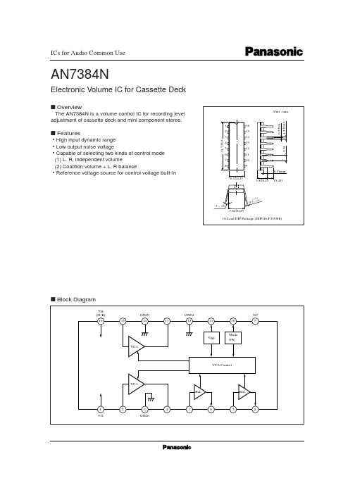
AN7384N中文资料
4 13
1.8kΩ
5
30µA
元器件交易网
AN7384N
s Pin Descriptions (Cont.)
Pin No.
Pin Name
Description
6
A-ch. Control Voltage Output
Control DC voltage buffer output pin
Tstg
ICs for Audio Common Use
Rating
Unit
±12
V
30
mA
800
mW
–20 ~ + 70
˚C
–55 ~ +150
˚C
s Recommended Operating Range (Ta = 25˚C)
Parameter Operating Supply Voltage Range
10
Volume Mode/Balance Low – independent volume control
Mode Switching
High – coalition volume balance control
mode
10
Vref 2
11
Reference Voltage Output
Reference voltage output pin
Negative Side Circuit Current Attenuation – 1 Attenuation – 2 Channel Balance – 1 Distortion Rate – 1 Distortion Rate – 2 Noise Output Voltage – 1 Noise Output Voltage – 2 Channel Balance – 2 Max. Input Voltage Max. Output Voltage Control Voltage Range
7383-G1C3-ATVA中文资料

元器件交易网EVERLIGHT ELECTRONICS CO.,LTD.Technical Data Sheet 7383/G1C3-ATVA/X/MSFeatures˙Popular T-1 3/4 diameter package. ˙Choice of various viewing angles. ˙Available on tape and reel. ˙Reliable and robust. ˙ESD-withstand voltage: up to 4KV. ˙The product itself will remain within RoHS compliant version. ˙UV resistant epoxyDescriptions˙The series is specially designed for applications requiring higher brightness. ˙The LED lamps are available with different colors, intensities, epoxy colors, etc. ˙Superior performance in outdoor environmentApplications˙Color Graphic Signs ˙Message boards ˙Variable message signs (VMS) ˙Commercial outdoor advertisingDevice Selection GuideLED Part No.7383/G1C3-ATVA/MS 7383/G1C3-ATVA/P/MSChip Mterial InGaN InGaNEmitted Color Super Green Super GreenLens Color Water Clear Water ClearStopper No YesEverlight Electronics Co., Ltd. Device Number : DLE-738-037http\\: Prepared date:05-26-2006Rev :1Page: 1 of 8Prepared : Grace Shen元器件交易网EVERLIGHT ELECTRONICS CO.,LTD.Technical Data Sheet 7383/G1C3-ATVA/X/MSPackage DimensionsStopper type No Stopper typeNotes: ˙All dimensions are in millimeters, tolerance is 0.25mm except being specified. ˙Lead spacing is measured where the lead emerges from the package. ˙Protruded resin under flange is 1.5mm Max LED.Everlight Electronics Co., Ltd. Device Number : DLE-738-037http\\: Prepared date:05-26-2006Rev :1Page: 2 of 8Prepared : Grace Shen元器件交易网EVERLIGHT ELECTRONICS CO.,LTD.Technical Data Sheet 7383/G1C3-ATVA/X/MSAbsolute Maximum Ratings (Ta=25℃)Parameter Forward Current Pulse Forward Current*1 Operating Temperature Storage Temperature Electrostatic Discharge*2Symbol IF IFP Topr Tstg ESD Tsol Pd Iz VRRating 30 100 -40 ~ +85 -40 ~ +100 4K 260 ±5 120 100 5Units mA mA ℃ ℃ V ℃ mW mA VSoldering Temperature Power Dissipation Zener Reverse Current Reverse VoltageNotes: *1:IFP Conditions--Pulse Width≦10msec and Duty≦1/10. *2:Soldering time≦5 seconds.Electro-Optical Characteristics (Ta=25℃)Parameter Forward Voltage Zener Reverse Voltage Luminous Intensity Viewing Angle Peak Wavelength Dominant Wavelength Spectrum Radiation Bandwidth Reverse Current Symbol VF Vz IV 2θ1/2 λp λd Δλ IR Condition IF=20mA IZ=5mA IF=20mA IF=20mA IF=20mA IF=20mA IF=20mA VR=5V Min. 2.8 5.2 7150 ----524 --Typ. ---30 518 528 35 -Max. 3.6 -14250 ----532 -50 Units V V mcd deg nm nm nm μAEverlight Electronics Co., Ltd. Device Number : DLE-738-037http\\: Prepared date:05-26-2006Rev :1Page: 3 of 8Prepared : Grace Shen元器件交易网EVERLIGHT ELECTRONICS CO.,LTD.Technical Data Sheet 7383/G1C3-ATVA/X/MSRank Combination (IF=20mA)Rank Luminous Intensity T 7150~9000 U 9000~11250 V 11250~14250Unit: :mcd*Measurement Uncertainty of Luminous Intensity: ±15%Rank Forward Voltage0 2.8~3.01 3.0~3.22 3.2~3.43 3.4~3.6Unit:V*Measurement Uncertainty of Forward Voltage: ±0.1VRank Dominant Wavelength12Unit:nm524~528 528~532 *Measurement Uncertainty of Dominant Wavelength ±1.0nm*The quantity ratio of the ranks is decided by EVERLIGHT.Everlight Electronics Co., Ltd. Device Number : DLE-738-037http\\: Prepared date:05-26-2006Rev :1Page: 4 of 8Prepared : Grace Shen元器件交易网EVERLIGHT ELECTRONICS CO.,LTD.Technical Data Sheet 7383/G1C3-ATVA/X/MSTypical Electro-Optical Characteristics CurvesEverlight Electronics Co., Ltd. Device Number : DLE-738-037http\\: Prepared date:05-26-2006Rev :1Page: 5 of 8Prepared : Grace Shen元器件交易网EVERLIGHT ELECTRONICS CO.,LTD.Technical Data Sheet 7383/G1C3-ATVA/X/MSPacking Quantity Specification1.500PCS/1Bag,5Bags/1Box 2.10Boxes/1CartonLabel Form SpecificationEVERLIGHT CPN: P/N: 7383/G1C3-ATVA/X/MS QTY: CAT: HUE: LOT NO: REF: MADE IN TAIWAN CPN: Customer’s Production Number P/N : Production Number QTY: Packing Quantity CAT: Ranks of Luminous Intensity and Forward Voltage HUE: Ranks of Dominant Wavelength REF: Reference LOT No: Lot Number MADE IN TAIWAN: Production PlaceEverlight Electronics Co., Ltd. Device Number : DLE-738-037http\\: Prepared date:05-26-2006Rev :1Page: 6 of 8Prepared : Grace Shen元器件交易网EVERLIGHT ELECTRONICS CO.,LTD.Technical Data Sheet 7383/G1C3-ATVA/X/MSNotes 1. Above specification may be changed without notice. EVERLIGHT will reserve authority on material change for above specification. 2. When using this product, please observe the absolute maximum ratings and the instructions for using outlined in these specification sheets. EVERLIGHT assumes no responsibility for any damage resulting from use of the product which does not comply with the absolute maximum ratings and the instructions included in these specification sheets. 3. These specification sheets include materials protected under copyright of EVERLIGHT corporation. Please don’t reproduce or cause anyone to reproduce them without EVERLIGHT’s consent. 4. Below the zener reference voltage Vz, all the current flows through LED and as the voltage rises to Vz, the zener diode “breakdown." If the voltage tries to rise above Vz current flows through the zener branch to keep the voltage at exactly Vz. 5. When the LED is connected using serial circuit, if either piece of LED is no light up but current can’t flow through causing others to light down. In new design, the LED is parallel with zener diode. if either piece of LED is no light up but current can flow through causing others to light up.Everlight Electronics Co., Ltd. Device Number : DLE-738-037http\\: Prepared date:05-26-2006Rev :1Page: 7 of 8Prepared : Grace Shen元器件交易网EVERLIGHT ELECTRONICS CO.,LTD.Technical Data Sheet 7383/G1C3-ATVA/X/MS6. Soldering ConditionCareful attention should be paid during soldering. When soldering, leave more then 3mm from solder joint to case, and soldering beyond the base of the tie bar is recommended. Avoiding applying any stress to the lead frame while the LEDs are at high temperature particularly when soldering. Recommended soldering conditions: Hand Soldering Temp. at tip of iron Soldering time Distance 400℃ Max. (30W Max.) 3 sec Max. 3mm Min.(From solder joint to case) Preheat temp. Bath temp. Bath time. Distance DIP Soldering 100℃ Max. (60 sec Max.) 265 Max. 5 sec Max. 3mm Min.EVERLIGHT ELECTRONICS CO., LTD. Office: No 25, Lane 76, Sec 3, Chung Yang Rd, Tucheng, Taipei 236, Taiwan, R.O.CTel: 886-2-2267-2000, 2267-9936 Fax: 886-2267-6244, 2267-6189, 2267-6306 http:\\Everlight Electronics Co., Ltd. Device Number : DLE-738-037http\\: Prepared date:05-26-2006Rev :1Page: 8 of 8Prepared : Grace Shen。
LS7366中文资料

GENERAL FEATURES:• Operating voltage: 3.0V to 5.5V (V DD - V SS )• 5V count frequency: 40MHz • 3V count frequency: 20MHz • 32-bit counter (CNTR).• 32-bit data register (DTR) and comparator.• 32-bit output register (OTR).• Two 8-bit mode registers (MDR0, MDR1) for programmable functional modes.• 8-bit instruction register (IR).• 8-bit status register (STR).• Latched Interrupt output on Carry or Borrow or Compare or Index.• Index driven counter load, output register load or counter reset.• Internal quadrature clock decoder and filter.• x1, x2 or x4 mode of quadrature counting.• Non-quadrature up/down counting.• Modulo-N, Non-recycle, Range-limit or Free-running modes of counting• 8-bit, 16-bit, 24-bit and 32-bit programmable configuration synchronous (SPI) serial interface• LS7366 (DIP); LS7366-S (SOIC); LS7366-TS (TSSOP) - See Figure 1-SPI/MICROWIRE (Serial Peripheral Interface):• Standard 4-wire connection: MOSI, MISO, SS/ and SCK. • Slave mode only.GENERAL DESCRIPTION:LS7366 is a 32-bit CMOS counter, with direct interface for quadra-ture clocks from incremental encoders. It also interfaces with the index signals from incremental encoders to perform variety of marker functions.For communications with microprocessors or microcontrollers, it provides a 4-wire SPI/MICROWIRE bus.The four standard bus I/Os are SS/, SCK, MISO and MOSI. The data transfer between a micro-controller and a slave LS7366 is synchronous. The synchronization is done by the SCK clocks supplied by the microcontroller.Each transmission is organized in blocks of 1 to 5 bytes of data. A transmission cycle is intitiated by a high to low transition of the SS/ input. The first byte received in a transmission cycle is always an instruction byte, whereas the second through the fifth bytes are always interpreted as data bytes. A transmission cycle is terminated with the low to high transition of the SS/ input. Received bytes are shifted in at the MOSI input, MSB first, with the leading edges (high transition) of the SCK clocks. Output data are shifted out on the MISO output, MSB first, with the trailing edges (low transition) of the SCK clocks.32-BIT QUADRATURE COUNTER WITH SERIAL INTERFACE1234567891011121314Vss V DD B A INDEX LFLAG/SS/SCK LS7366MISO MOSIf CKi f CKO PIN ASSIGNMENT TOP VIEWCNT_EN DFLAG/FIGURE 1LSI/CSILSI Computer Systems, Inc. 1235 Walt Whitman Road, Melville, NY 11747 (631) 271-0400 FAX (631) 271-0405LS7366U L®A3800January 2005Read and write commands cannot be combined.For example, when the device is shifting out read data on MISO output, it ignores the MOSI input,even though the SS/ input is active. SS/ must be terminated and reasserted before the device will accept a new command.The counter can be configured to operate as a 1, 2, 3 or 4-byte counter. When configured as a n-byte counter, the CNTR, DTR and OTR are all configured as n-byte registers, where n = 1, 2, 3 or 4. The content of the instruction/data identity is automatically adjusted to match the n-byte configu-ration. For example, if the counter is configured as a 2-byte counter, the instruction “write to DTR”expects 2 data bytes following the instruction byte.If the counter is configured as a 3-byte counter, the same instruction will expect 3 bytes of data follow-ing the instruction byte.Following the transfer of the appropriate number of bytes any further attempt of data transfer is ignored until a new instruction cycle is started by switching the SS/ input to high and then low.The counter can be programmed to operate in a number of different modes, with the operating characteristics being written into the two mode registers MDR0 and MDR1. Hardware I/Os are provided for event driven operations, such as processor interrupt and index related functions.I/O Pins:Following is a description of all the input/output pins.A (Pin 12)B (Pin 11)Inputs. A and B quadrature clock outputs from incremental encoders are directly applied to the A and B inputs of the LS7366. These clocks are ideally 90 degrees out-of-phase signals. A and B inputs are validated by on-chip digital filters and then decoded for up/down direction and count clocks.In non-quadrature mode, A serves as the count input andB serves as the direction input (B = high enables up count, B = low enables down count). In non-quadrature mode,the A and B inputs are not filtered internally, and are instantaneous in nature.INDEX (Pin 10)Input. The INDEX is a programmable input that canbe driven directly by the Index output of an incremental encoder. It can be programmed via the MDR to functionas one of the following:LCNTR (load CNTR with data from DTR), RCNTR(reset CNTR), or LOTR (load OTR with data from CNTR). Alternatively, the INDEX input can be masked out for"no functionality".In quadrature mode, the INDEX input is validated with the filter clock in order to synchronize with the quadrature inputs A and B. To be valid, the INDEX signal in quadrature mode must overlap the condition in which both A and B are low or both A and B are high. In non-quadrature mode, however, the INDEX input is instantaneous in nature and totally independent of A and B.f CK i (Pin 2), f CK0 (Pin 1)Input, Output. A crystal connected between these 2 pins generates the basic clock for filtering the A, B and INDEX inputs in the quadrature count mode. Instead of a crystal the f CKi input may also be driven by an external clock.The frequency at the f CKi input is either divided by 2(if MDR0 <B7> = 1) or divided by 1 (if MDR0 <B7> = 0)for the filter circuit. For proper filtering of the A, B andthe Index inputs the following condition must be satisfied:f f≥ 4f QAWhere f f is the internal filter clock frequency derived from the fCKi in accordance with the status of MDR0 <B7> and f QA is the maximum frequency of Clock A in quadrature mode.In non-quadrature count mode, f CKi is not used and should be tied off to any stable logic state.SS/ (Pin 4)A high to low transition at the SS/ (Slave Select) input selects the LS7366 for serial bi-directional data transfer;a low to high transition disables serial data transferand brings the MISO output to high impedance state.This allows for the accommodation of multiple slave units on the serial I/O.CNT_EN (Pin 12)Input. Counting is enabled when CNT_EN input is high; counting is disabled when this input is low.There is an internal pull-up resistor on this input.LFLAG/ (Pin 8), DFLAG/ (Pin 9)Outputs. LFLAG/ and DFLAG/ are programmable outputs to flag the occurences of Carry (counter overflow), Borrow (counter underflow), Compare (CNTR = DTR) and INDEX. The LFLAG/ is an open drain latched output. In contrast, the DFLAG/ is a push-pull instantaneous output. The LFLAG/ can be wired in multi-slave configuration, forming a single processor interrupt line. When active LFLAG/ switches to logic 0 and can be restored to the high impedence state only by clearing the status register, STR. In contrast, the DFLAG/ dynamically switches low with occurences of Carry, Borrow, Compare and INDEX conditions. The configuration of LFLAG/ and DFLAG/ are made through the control register MDR1. In free-running count mode LFLAG/ and DFLAG/ output the same status information in latched and dynamic form, respectively. In single-cycle mode the DFLAG/ outputs CY and BW signals independent of the MDR1 configura-tion. In range-limit and modulo-n modes, DFLAG/ outputs CMP signal in count-up direction (at CNTR = DTR) and BW signal when CNTR underflows independent of the MDR1 configuration. In effect, DFLAG/ generates mode-relevant marker signals in all modes, excepting the free-running count mode wherein MDR1 configures the output signal selection.MOSI (RXD) (Pin 7)Input. Serial output data from the host processor is shifted into the LS7366 at this input.MISO (TXD) (Pin 6)Output. Serial output data from the LS7366 is shifted out on the MISO (Master In Slave Out) pin. The MISO output goes into high impedance state when SS/ input is at logic high, providing multiple slave-unit serial outputs to be wire-ORed.SCK (Pin 5)Input. The SCK input serves as the shift clock input for transmit-ting data in and out of LS7366 on the MOSI and the MISO pins, respectively. Since the LS7366 can operate only in the slave mode, the SCK signal is provided by the host processor as a means for synchronizing the serial transmission between itself and the slave LS7366.REGISTERS:The following is a list of LS7366 internal registers:Upon power-up the registers DTR, CNTR, STR, MDR0 and MDR1 are reset to zero.DTR. The DTR is a software configurable 8, 16, 24 or 32-bit input data register which can be written into directly from MOSI, the serial input. The DTR data can be transferred into the 32-bit counter (CNTR) under program control or by hardware index signal. The DTR can be cleared to zero by software control.In certain count modes, such as modulo-n and range-limit,DTR holds the data for "n" and the count range, respectively.In compare operations, whereby compare flag is set, the DTR is compared with the CNTR.STR. The STR is an 8-bit status register which stores count related status information.CY BW CMP IDX CEN PLS U/D S 7 6 5 4 3 2 1 0CY: Carry (CNTR overflow) latchBW: Borrow (CNTR underflow) latch CMP: Compare (CNTR = DTR) latch IDX: Index latchCEN: Count enable status: 0: counting disabled, 1: counting enabled7366-012405-3IR . The IR is an 8-bit register that fetches instruction bytes from the received data stream and executes them to perform such functions as setting up the operating mode for the chip (load the MDR) and data transfer among the various registers.B7 B6 B5 B4 B3 B2 B1 B0B2 B1 B0 = XXX (Don’t care)B5 B4 B3 = 000: Select none= 001: Select MDR0 = 010: Select MDR1= 011: Select DTR = 100: Select CNTR = 101: Select OTR = 110: Select STR = 111: Select noneB7 B6 = 00: CLR register= 01: RD register = 10: WR register = 11: LOAD register The actions of the four functions, CLR, RD, WR and LOAD are elaborated in Table 1.TABLE 1Number of Bytes OP Code Register OperationMDR0Clear MDR0 to zero MRD1Clear MDR1 to zero1 CLR DTR NoneCNTR Clear CNTR to zero OTR None STR Clear STR to zero MDR0Output MDR0 serially on TXD (MISO)MDR1Output MDR1 serially on TXD (MISO)2 to 5 RD DTR NoneCNTR Transfer CNTR to OTR, then output OTR seriallyon TXD (MISO)OTR Output OTR serially on TXD (MISO)STR Output STR serially on TXD (MISO)MDR0Write serial data at RXD (MOSI) into MDR0MDR1Write serial data at RXD (MOSI) into MDR12 to 5 WR DTR Write serial data at RXD (MOSI) into DTRCNTR None OTR None STR None MDR0None MDR1None1 LOAD DTR NoneCNTR Transfer DTR to CNTR in “parallel”OTR Transfer CNTR to OTR in “parallel”CNTR. The CNTR is a software configurable 8, 16, 24 or 32-bit up/down counter which counts the up/down pulses resulting from the quadrature clocks applied at the A and B inputs, or alternatively, in non-quadrature mode, pulses applied at the A input. By means of IR intructions the CNTR can be cleared, loaded from the DTR or in turn, can be transferred into the OTR. The “clear CNTR”and the “load CNTR” commands in the ”range-limit” mode, however have limitations. In this mode when the CNTR is frozen in up count direction at CNTR = DTR, a “clear CNTR” command will only function if the count direction is reversed from up to down. Similarly, in the down direction at CNTR = 0, a “load CNTR” command will only function if the direction is reversed from down to up.OTR. The OTR is a software configuration 8, 16, 24 or 32-bit register which can be read back on the MISO output. Since instantaneous CNTR value is often needed to be read while the CNTR continues to count, the OTR serves as a convenient dump site for instantaneous CNTR data which can then be read without interfering with the counting process.PLS: Power loss indicator latch; set upon power upU/D: Count direction indicator: 0: count down, 1: count up S: Sign bit. 1: negative, 2: positiveA “CLR STR” command to IR resets all status bits except CEN and U/D. In quadrature mode, if the quadrature clocks have been halted, the status bits CY, BW and CMP are not affected by a “CLR STR” command under the following conditions: CY: If CNTR = FFFFFFFF with status bit U/D = 1 BW: If CNTR = 0 with status bit U/D = 0 CMP: If CNTR = DTRIn non-quadrature mode the same rules apply if input A is held at logic low.7366-112204-4ABSOLUTE MAXIMUM RATINGS: (All voltages referenced to Vss)Parameter Symbol Values Unit DC Supply Voltage V DD +7.0V Voltage V IN Vss - 0.3 to V DD + 0.3 VOperating Temperature T A -25 to +85o C Storage Temperature T STG -65 to +150o C MDR1. The MDR1 (Mode Register 1) is an 8-bit read/write register which is appended to MDR0 for additional modes. Upon power-up MDR1 is cleared to zero.B7 B6 B5 B4 B3 B2 B1 B0B1 B0 = 00: 4-byte counter mode = 01: 3-byte counter mode = 10: 2-byte counter mode. = 11: 1-byte counter mode B2 = 0: Enable counting = 1: Disable counting B3 = : not used B4 = 0: NOP= 1: FLAG on IDX (B4 of STR) B5 = 0: NOP= 1: FLAG on CMP (B5 of STR) B6 = 0: NOP= 1: FLAG on BW (B6 of STR) B7 = 0: NOP= 1: FLAG on CY (B7 of STR)MDR0. The MDR0 (Mode Register 0) is an 8-bit read/write register that sets up the operating mode for the LS7366. The MDR0 is written into by executing the "write-to-MDR0" instruction via the instruction register. Upon power up MDR0 is cleared to zero. The following is a breakdown of the MDR bits:B7 B6 B5 B4 B3 B2 B1 B0B1 B0 = 00: non-quadrature count mode. (A = clock, B = direction). = 01: x1 quadrature count mode (one count per quadrature cycle). = 10: x2 quadrature count mode (two counts per quadrature cycle). = 11: x4 quadrature count mode (four counts per quadrature cycle).B3 B2 = 00: free-running count mode.= 01: single-cycle count mode (counter disabled with carry or borrow, re-enabled with reset or load). = 10: range-limit count mode (up and down count-ranges are limited between DTR and zero, respectively; counting freezes at these limits but resumes when direction reverses). = 11: modulo-n count mode (input count clock frequency is divided by a factor of (n+1), where n = DTR, in both up and down directions).B5 B4 = 00: disable index.= 01: configure index as the "load CNTR" input (transfers DTR to CNTR). = 10: configure index as the "reset CNTR" input (clears CNTR to 0). = 11: configure index as the "load OTR" input (transfers CNTR to OTR). B6 = 0: Negative index input = 1: Positive index inputB7 = 0: Filter clock division factor = 1 = 1: Filter clock division factor = 2NOTE: Applicable to both LFLAG/ and DFLAG/DC Electrical Characteristics. (T A = -25˚C to +85°C)Parameter Symbol Min. TYP Max. Unit RemarksSupply Voltage V DD 3.0- 5.5V-Supply Current I DD300400450µA V DD = 3.0VI DD700800950µA V DD = 5.0VInput Voltagesf CK i, Logic high V CH- 2.1 2.3V V DD = 3.0VV CH- 3.5 3.7V V DD = 5.0Vf CKi, Logic Low V CL0.70.9-V V DD = 3.0VV CL 1.3 1.5-V V DD = 5.0VAll other inputs, Logic High V AH- 1.9 2.1V V DD = 3.0VV AH- 3.2 3.5V V DD = 5.0VAll other inputs, Logic Low V AL0.50.7-V V DD = 3.0VV AL 1.0 1.2-V V DD = 5.0VInput Currents:CNT_EN Low I IEL- 3.0 5.0µA V AL = 0.7V, V DD = 3.0VI IEL-10.015.0µA V AL = 1.2V, V DD = 5.0V CNT_EN High I IEH- 1.0 3.0µA V AH = 1.9V, V DD = 3.0VI IEH- 4.0 6.0µA V AH = 3.2V, V DD = 5.0V All other inputs, High or Low--00µA-Output Currents:FLAG Sink I OFL-1.3-2.0-mA V OUT = 0.5V, V DD = 3.0VI OFL-3.2-4.0-mA V OUT = 0.5V, V DD = 5.0V FLAG Source- 0 0-mA Open Drain Outputf CKO Sink I OCL-1.3-2.0-mA V OUT = 0.5V, V DD = 3.0VI OCL-3.2-4.0-mA V OUT = 0.5V, V DD = 5.0V f CKO Source I OCH 1.3 2.0-mA V OUT = 2.5V, V DD = 3.0VI OCH 3.2 4.0-mA V OUT = 4.5V, V DD = 5.0V TXD/MISO:Sink I OML-1.5-2.4-mA V OUT = 0.5V, V DD = 3.0VI OML-3.8-4.8-mA V OUT = 0.5V, V DD = 5.0V Source I OMH 1.5 2.4-mA V OUT = 0.5V, V DD = 3.0VI OMH 3.8 4.8-mA V OUT = 0.5V, V DD = 5.0V Transient Characteristics. (T A = -25˚C to +85˚C, V DD = 5V ± 10%)Parameter Symbol Min. Value Max.Value Unit Remarks(See Fig. 2 & 3)SCK High Pulse Width t CH100-ns-SCK Low Pulse Width t CL100-ns-SS/ Set Up Time t CSL100-ns-SS/ Hold Time t CSH100-ns-Quadrature Mode(See Fig. 4, 6 & 7)f CKI High Pulse Width t112-ns-f CKI Pulse Width t212-ns-f CKI Frequency f FCK-40MHz-Effective Filter Clock fF Period t325-ns t3 = t1+t2, MDR0 <7> = 0t350-ns t3 = 2(t1+t2), MDR0 <7> = 1 Effective Filter Clock f F frequency f F-40MHz f F = 1/ t3Quadrature Separation t426-ns t4 > t3Quadrature Clock Pulse Width t552-ns t5≥ 2t3Quadrature Clock frequency f QA, f QB-9.6MHz f QA = f QB < 1/4t3 Quadrature Clock to Count Delay t Q14t35t3--x1 / x2 / x4 Count Clock Pulse Width t Q212-ns t Q2 = (t3)/2Index Input Pulse Width ti d32-ns t id > t4Index Set Up Time ti s-5ns-Index Hold Time ti h-5ns-Quadrature clock to t fl 4.5t3 5.5t3ns-DFLAG/ or LFLAG/ delayDFLAG/ output width t fw26-ns t fw = t4Parameter Symbol Min. Value Max.Value Unit RemarksNon-Quadrature Mode(See Fig. 5 & 8)Clock A - High Pulse Width t612-ns-Clock A - Low Pulse Width t712-ns-Direction Input B Set-up Time t8S12-ns-Direction Input B Hold Time t8H10-ns-Clock Frequency (non-Mod-N)f A-40MHz f A = (1/(t6 + t7))Clock to DFLAG/ or t920-ns-LFLAG/ delayDFLAG/ output width t1012-ns t10 = t7Transient Characteristics. (T A = -25˚C to +85˚C, V DD = 3.3V ± 10%)Parameter Symbol Min. Value Max.Value Unit Remarks(See Fig. 2 & 3)SCK High Pulse Width t CH120-ns-SCK Low Pulse Width t CL120-ns-SS/ Set Up Time t CSL120-ns-SS/ Hold Time t CSH120-ns-Quadrature Mode(See Fig. 4, 6 & 7)f CKI High Pulse Width t124-ns-f CKI Pulse Width t224-ns-f CKI Frequency f FCK-20MHz-Effective Filter Clock fF Period t350-ns t3 = t1+t2, MDR0 <7> = 0t3100-ns t3 = 2(t1+t2), MDR0 <7> = 1 Effective Filter Clock f F frequency f F-20MHz f F = 1/t3Quadrature Separation t452-ns t4 > t3Quadrature Clock Pulse Width t5105-ns t5≥ 2t3Quadrature Clock frequency f QA, f QB- 4.5MHz f QA = f QB < 1/4t3 Quadrature Clock to Count Delay t Q14t35t3--x1/x2/x4 Count Clock Pulse Width t Q225-ns t Q2 = (t3)/2Index Input Pulse Width t id60-ns t id > t4Index Set Up Time t is-10ns-Index Hold Time t ih-10ns-Quadrature clock to t fl 4.5t3 5.5t3ns-DFLAG/ or LFLAG/ delayDFLAG/ output width t fw52-ns t fw = t4Non-Quadrature Mode(See Fig. 5 & 8)Clock A - High Pulse Width t624-ns-Clock A - Low Pulse Width t724-ns-Direction Input B Set-up Time t8S24-ns-Direction Input B Hold Time t8H24-ns-Clock Frequency (non-Mod-N)f A-40MHz f A = (1/(t6 + t7))Clock to DFLAG/or t940-ns-LFLAG/ delayDFLAG/ output width t1024-ns t10 = t7。
LA76810功能参数

LA76810LA76810是三洋公司于99年开发成功的用于PAL/NTSC 制彩色电视信号处理的大规模集成电路单片可完成图像伴音的解调色解码亮度处理同步及行场小信号的处理LA76810集成度高外围元件少用于替代三洋A6机芯的LA7687A 单片被称为A12机芯LA76810具有以下特点单片多制式适用于处理PAL/NTSC 视频信号配合免调试SECAM 解码电路可实现全制式解码采用PLL 图像和伴音解调采用单晶体完成PAL NTSC 制信号解调内藏一行基带延迟线亮度延迟线不需外接各种带通滤波器陷波器内置伴音和视频选择开关50/60Hz 场频自动识别I 2C 总线控制等芯片还内置了峰化清晰度改善电路挖芯降噪处理电路黑电平延伸电路对比度改善电路等A12机芯电视整机线路比较简单外接元件也很少便于生产与维修海信电器股份有限公司在2000年研制投产了A12单片机芯并在升级彩电系列休闲系列及环保二代系列产品中大量使用其主要机型有TC1410L TC1423TC2102G TC2110L TC2166L TC2175G TC2181F TC2199A TC2505TC2540AM TC2588D TC2961L TC2975DL TC2999L TF2110D 等对地阻值k 引脚序号标 号 功 能 电压值V 黑笔接地 红笔接地1 AUDIO OUT 伴音输出 2.25 8.5 9.12 FM OUT 伴音调频解调 2.37 9.4 11.03 PIF AGC 中放AGC 滤波 2.40 9.8 11.4 4 RF AGC OUT 高放AGC 输出 3.50 9.4 33.05 PIF IN 中频输入 2.85 9.5 9.96 PIF IN 中频输入 2.85 9.5 9.97 IF GND 中频电路地 0 0 08 VCC(VIF) 图像中频供电 4.90 1.4 1.49 FM FIL 调频解调滤波 2.20 9.8 12.2 10 AFT OUT AFT 信号输出 2.40 7.5 10.5 11 BUS DATA 总线数据线 4.50 8.0 12.5 12 BUS CLOCK 总线时钟线 4.48 7.9 12.5 13 ABL 自动亮度限制输入 2.21 6.4 8.0 14 R IN 字符红信号输入 0.02 9.4 10.8 15 G IN 字符绿信号输入 0.02 9.4 10.8 16 B IN 字符蓝信号输入 0.02 9.4 10.8 17 BL IN 字符消隐信号输入 0.80 3.3 3.3 18 VCC(RGB) RGB 电路供电 8.24 1.0 0.9 19 R OUT 红信号输出 2.46 9.0 8.5 20 G OUT 绿信号输出 2.50 9.1 8.5 21 B OUT 蓝信号输出 2.55 9.3 8.5 22 SYNC 同步信号输出 0.37 7.3 10.6 23 V OUT 场激励信号输出 2.60 2.0 2.0 24 V RAMP ALC FIL 场信号形成滤波 2.07 9.5 11.0 25 VCC(H/D) 行场激励信号电路供电 5.10 1.0 1.026 AFC FIL AFC 滤波 2.56 9.5 11.5 27 H.OUT 行激励信号输出 0.64 2.2 2.2 28 FBP IN 反馈脉冲输入 1.12 9.2 10.1REF行振荡参考输入 1.63 4.7 4.729 IOUT 行振荡信号输出 0.64 6.6 11.630 CLOCK1.4 1.431 1 HDL VCC 1行延迟线供电 4.5032 1 HDL VCC OUT 1行延迟线自举升压 8.30 633 GND 1行延迟/行电路地 0 0 034 SECAM B-Y IN SECAM蓝色差输入 2.50 9.6 10.735 SECAM R-Y IN SECAM红色差输入 2.50 9.6 10.711.236 C AFC2 FIL 彩色AFC2滤波 3.9010.011.79.8OUT SECAM制使用 2.6337 FSC9.911.1 38 XTAL 晶振 3.789.5 10.639 C AFC1 FIL 彩色AFC1滤波 3.30V.OUT 视频信号选择输出 2.20 9.5 11.440 SELECT41 GND(V/C/D) 地 0V.IN 外部视频信号输入 2.50 9.6 11.242 EXT1.4 43 VCC(V/C/D) 供电 5.031.4V.IN 内部视频信号输入 2.80 9.5 11.544 INTSTR 黑电平延伸滤波 2.60 8.0 8.645 BLACK1.2 1.2OUT 视频信号输出 2.7046 VIDEOFIL 38MHz解调APC滤波 3.95 9.5 11.647 APC1.8 1.848 VCOCOIL 中频解调中周 4.201.8 1.8COIL 中频解调中周 4.2049 VCOFIL 压控振荡器滤波 2.40 9.1 11.050 VCO51 EXT AUDIO IN 外部音频信号输入 2.10 9.5 11.111.59.152 SIFOUT 伴音中频输出 1.9053 SIF APC FIL 伴音解调APC滤波 2.20 9.4 11.511.69.654 SIFIN 伴音中频输入 3.10说明测量机型为海信TC2199A采用MF10B型万用表在线电阻采用R1k挡。
AN13300A资料
7 8
Note) *:
Supply current Power dissipation
ICC PD
mA W
Expect for the operating ambient temperature and storage temperature , all ratings are for Ta = 25°C.
DATA SHEET
Part No. Package Code No.
AN13300A
*SOP022 - P - 0375C
SEMICONDUCTOR COMPANY MATSUSHITA ELECTRIC INDUSTRIAL CO., LTD.
Publication date: January 2005
2003 SEP
SDF00039AEB
1
AN13300A Contents
Features …………………………………………………………………………………………………………… 3 Applications ………………………………………………………………………………………………………… 3 Package ……………………………………………………………………………………………………………. 3 Block Diagram ………………………………………………………………………………………………………. 4 Pin Descriptions …………………………………………………………………………………………………… 4 Absolute Maximum Ratings ………………………………………………………………………………………. 5 Operating Supply Voltage Range ………………………………………………………………………………. 5
AU6366中文资料

AU6366USB2.0 Single LUNMultiple Flash Card Reader Controller Technical Reference ManualAU6366USB2.0 Single LUN Multiple Flash Card Reader ControllerC o p y r i g h tCopyright © 1997 - 2007. Alcor Micro, Corp. All Rights Reserved. No part of this data sheet may be reproduced, transmitted, transcribed, stored in a retrieval system or translated into any language or computer language, in any form or by any means, electronic, mechanical, magnetic, optical, chemical, manual or otherwise, without prior written permission from Alcor Micro, Corp.T r a d e m a r k A c k n o w l e d g e m e n t sThe company and product names mentioned in this document may be the trademarks or registered trademarks of their manufacturers.D i s c l a i m e rAlcor Micro, Corp. reserves the right to change this product without prior notice. Alcor Micro, Corp. makes no warranty for the use of its products and bears no responsibility for any error that appear in this document. Specifications are subject to change without prior notice.R e v i s i o n H i s t o r yDate Revision DescriptionJan 2006 1.00W Official ReleaseAug 2006 1.01W Update new address of Los Angeles OfficeNov 2006 1.02W Modify “1.2 Features”July 2007 1.03W Modify “5.6 Power Switch Feature”C o n t a c t I n f o r m a t i o n:Web site: /Taiwan China ShenZhen OfficeAlcor Micro, Corp. Rm.2407-08, Industrial Bank Building 4F, No 200 Kang Chien Rd., Nei Hu, No.4013, Shennan Road,Taipei, Taiwan, R.O.C. ShenZhen,China. 518026Phone: 886-2-8751-1984 Phone: (0755) 8366-9039Fax: 886-2-2659-7723 Fax: (0755) 8366-9101Santa Clara Office Los Angeles Office2901 Tasman Drive, Suite 206 9070 Rancho Park CourtSanta Clara, CA 95054 Rancho Cucamonga, CA 91730USA USA Phone: (408) 845-9300 Phone: (909) 483-9900Fax: (408) 845-9086 Fax: (909) 944-0464<Memo>Table of Contents1. Introduction (1)1.1 Description (1)1.2 Features (1)2. Application Block Diagram (2)3. Pin Assignment (3)4. System Architecture and Reference Design (6)4.1 AU6366 Block Diagram (6)5. Electrical Characteristics (7)5.1 Absolute Maximum Ratings (7)5.2 Recommended Operating Conditions (7)5.3 General DC Characteristics (7)5.4 DC Electrical Characteristics of 3.3V I/O Cells (8)5.5 USB Transceiver Characteristics (8)5.6 Power Switch Feature (12)6. Mechanical Information (13)7. Abbreviations (14)iList of FiguresFigure 2.1 Block Diagram (2)Figure 3.1 Pin Assignment Diagram (3)Figure 4.1 AU6366 Block Diagram (6)Figure 5.1 Built-in card power switch I-V curve (12)Figure 5.2 Card Detect Power-on Timing (12)Figure 6.1 Mechanical Information Diagram (13)List of TablesTable 3.1 Pin Descriptions (4)Table 5.1 Absolute Maximum Ratings (7)Table 5.2 Recommended Operating Conditions (7)Table 5.3 General DC Characteristics (7)Table 5.4 DC Electrical Characteristics of 3.3V I/O Cells (8)Table 5.5 Electrical characteristics (8)Table 5.6 Static characteristic:Digital pin (9)Table 5.7 Static characteristic:Analog I/O pins(DP/DM) (9)Table 5.8 Dynamic characteristic:Analog I/O pins(DP/DM) (10)ii1. Introduction1.1D e s c r i p t i o nThe AU6366 is a single chip integrated USB 2.0 multimedia card reader controller that enables PC/DVD/Printer to read/write various type of flash media cards. Flash media cards such as CF, SMC, XD, SD, MMC, Memory Stick are widely used in digital camera, cell phone, PDA and MP3 player to store digital photos and compressed music.Performance of AU6366 is maximized by implementing the latest and fastest card specification available form the industry.The AU6366 is designed in shared pin architecture to meet cost and space regulate for Notebook end reunite.1.2F e a t u r e sSupport USB V2.0 specification and USB Device Class Definition for Mass Storage, Bulk-Transport V1.0Support CF/MD/SD/MMC/MS/MS_Pro/MS_Duo/xD/SMC compatible flash cardSupport the latest flash card specification: CF 3.0 (16-bit IDE mode), SD1.1 (HS-SD), MMC4.0 (8-bit), MSPro parallel mode (4-bit), xD 1.2 Hardware DMA engine integrated for performance enhancementWork with default driver from Windows ME/2000/XP and Mac OS X; Windows 98/2000(SP1/SP2) and Mac OS 9 are supported by vendor driver fromAlcor.Ping-pong FIFO implementation for concurrent bus operationSupport multiple sectors transfer optimize performanceSupport slot-to-slot read/write operationSupport Dynamic Icon UtilitySupport LED for bus operating indicationPower switch integrated to reduce production BOM cost30MHz 8051 CPUBuilt in 3.3V to 2.5V regulatorRun at 12MHz crystalAvailable in 48-pin LQFP packageAU6366 USB 2.0 Single LUN Multiple Flash Card Reader Controller V1.03W 12. Application Block DiagramThe following application drawing demonstrates a typical card reader block diagram using AU6366. By connecting one card reader to a desktop or notebook PC through USB bus, the AU6366 becomes a bus-powered, high speed USB card reader, which can be used as a bridge for data transfer between Desktop PC and Notebook PC.Figure 2.1 Block DiagramSMC/SD/MMCAU6366AU6366 USB 2.0 Single LUN Multiple Flash Card Reader Controller V1.03W 2AU6366 USB 2.0 Single LUN Multiple Flash Card Reader Controller V1.03W33. Pin AssignmentThe AU6366 is delivered in 48pin LQFP form factor. Documented below is a figure shows signal names of each pin and a table in the following page describes each pin in more details.Figure 3.1 Pin Assignment DiagramCARDDATA15CFWTN CLEDCHIPRESETN GNDAVDDARPUAVDD DPDMAVSS RREFXDCDNCONTROLOUT5CONTROLOUT4CONTROLOUT3CONTROLOUT2CONTROLOUT1CONTROLOUT0VDDCARDDATA1CARDDATA2GNDCARDDATA0SDCDNVSSHCPWR_V33SMCDNCFCDNMSINSVDD25VPVSSPVDDXOVDDHXICARDDATA3CARDDATA4CARDDATA5CARDDATA6CARDDATA7CARDDATA8CARDDATA9CARDDATA10CARDDATA11CARDDATA12CARDDATA14CARDDATA13AU6366 USB 2.0 Single LUN Multiple Flash Card Reader Controller V1.03W4Table 3.1 Pin DescriptionsPin #Pin NameI/ODescription1 CARDDATA15 I/O CF Data15/xD Data72 CFWTN I CF WAITN3 CLED O Card Operating LED4 CHIPRESETNI Chip Reset, Pull up with RC 5 GNDA PLL Ground 6 VDDA I PLL VDD 2.5V7 RPU I Connected with an 1.5k pull up resistor to 3.3 VDD 8 AVDD I Analog Power 3.3V 9 DP I/O DP 10 DM I/O DM11 AVSS Analog Ground12 RREF I Connected an 1k resistor to GND for impedance match13 PVDD I OSC Power 3.3V 14 XI I 12 MHz crystal input. 15 XO O 12 MHz crystal output. 16 PVSS OSC Ground 17 VDD25V O Core Power 2.5V 18 VDDH I 3.3V for IO pad 19 CPWR_V33 O Card Power 3.3V 20 VSSH Power Ground 21 MSINS I MS INS22 SMCDN I SMC Card Detect 23 CFCDN I CF Card Detect 24 SDCDN I SD Card Detect 25 XDCDN I xD Card Detect26 CONTROLOUT5 O CFRESETN and SMWRN/XDWRN 27 CONTROLOUT4 O CFWRN and SMRDN/XDRDN 28 CONTROLOUT3 O CFRDN and XDCEN/SMCEN 29CONTROLOUT2OCFAD2 and SMALE/XDALEAU6366 USB 2.0 Single LUN Multiple Flash Card Reader Controller V1.03W5Pin #Pin NameI/ODescription30 CONTROLOUT1 O CFAD1, MSCLK and SMCLE/XDCLE 31 CONTROLOUT0O CFAD0, SDCLK and MSBS 32 VDD I Core power 2.5V 33 GND Core Ground34 CARDDATA0 I/O CFDATA0, MSDATA0,and SDCMD 35 CARDDATA1 I/O CFDATA1,MSDATA1,XDWPN,and SMWPN 36 CARDDATA2 I/O CFDATA2,MSDATA2,and SDWP37 CARDDATA3 I/O CFDATA3,MSDATA3,SMRBN,and XDRBN 38 CARDDATA4 I/O CFDATA4 and SDDATA0 39 CARDDATA5 I/O CFDATA5 and SDDATA1 40 CARDDATA6 I/O CFDATA6 and SDDATA2 41 CARDDATA7 I/O CFDATA7 and SDDATA342 CARDDATA8 I/O CFDATA8,XDDATA0, and SDDATA4 43 CARDDATA9 I/O CFDATA9,XDDATA1, and SDDATA5 44 CARDDATA10 I/O CFDATA10,XDDATA2, and SDDATA6 45 CARDDATA11 I/O CFDATA11,XDDATA3, and SDDATA7 46 CARDDATA12 I/O CFDATA12 and XDDATA4 47 CARDDATA13 I/O CFDADA13 and XDDATA5 48CARDDATA14I/OCFDATA14 and XDDATA64. System Architecture and Reference Design4.1 A U 6366 B l o c k D i a g r a mFigure 4.1 AU6366 Block DiagramCF MD SMC SD MMC MS xDUSB Upstream PortAU6366 USB 2.0 Single LUN Multiple Flash Card Reader Controller V1.03W65. Electrical Characteristics5.1A b s o l u t e M a x i m u m R a t i n g sTable 5.1 Absolute Maximum RatingsSYMBOL PARAMETER RATING UNITS V DDH Power Supply -0.3 to V DDH +0.3 VV IN Input Signal Voltage -0.3 to 3.6 VV OUT Output Signal Voltage-0.3 to V DDH +0.3 VT STG Storage Temperature-40 to 150 O C5.2 Recommended Operating ConditionsTable 5.2 Recommended Operating ConditionsSYMBOL PARAMETER MIN TYP MAX UNITS V DDH Power Supply 3.0 3.3 3.6 V V DD Digital Supply 2.25 2.5 2.75 V V IN Input Signal Voltage 0 3.3 3.6 V T OPR Operating Temperature 0 70 O C 5.3G e n e r a l D C C h a r a c t e r i s t i c sTable 5.3 General DC CharacteristicsSYMBOL PARAMETER CONDITIONS MIN TYP MAX UNITSI IN Input current No pull-up orpull-down-10 ±1 10 µAI OZ Tri-state leakage current-10 ±1 10 µA C IN Input capacitance Pad Limit 2.8 ρF C OUT Output capacitance Pad Limit 2.8 ρFC BID Bi-directional buffercapacitancePad Limit 2.8 ρFAU6366 USB 2.0 Single LUN Multiple Flash Card Reader Controller V1.03W 75.4D C E l e c t r i c a l C h a r a c t e r i s t i c s o f3.3V I/O C e l l sTable 5.4 DC Electrical Characteristics of 3.3V I/O CellsLimitsSYMBOL PARAMETER CONDITIONSMIN TYP MAXUNIT V DDH Power supply 3.3V I/O 3.0 3.3 3.6 V V il Input low voltage 0.8 VV ih Input high voltage LVTTL2.0 VV ol Output low voltage ∣I ol∣=2~16mA 0.4 V V oh Output high voltage ∣I oh∣=2~16mA 2.4 V R pu Input pull-up resistance PU=high, PD=low55 75 190 KΩR pd Input pull-down resistance PU=low, PD=high40 75 190 KΩI in Input leakage current V in= V DDH or 0 -10 ±1 10 μAI oz Tri-state output leakagecurrent-10 ±1 10 μA5.5U S B T r a n s c e i v e r C h a r a c t e r i s t i c sTable 5.5 Electrical characteristicsSymbol Parameter Conditions Min.Typ. Max.Unit VD33 Analog supply Voltage 3.0 3.3 3.6 V VDDUVDDADigital supply Voltage 2.25 2.5 2.75 VI CC Operating supply current High speed operatingat 480 MHz73mAI CC (susp)Suspend supply currentIn suspend mode,current with 1.5kΩpull-up resistor on pinRPU disconnected120µAAU6366 USB 2.0 Single LUN Multiple Flash Card Reader Controller V1.03W 8Table 5.6 Static characteristic:Digital pinSymbol Parameter Conditions Min. Typ. Max. UnitInput levelsV IL Low-level input voltage 0.8 V V IH High-level input voltage 2.0 VOutput levelsV OL Low-level output voltage 0.2 V V OH High-level output voltage VDDH-0.2V Table 5.7 Static characteristic:Analog I/O pins(DP/DM)Symbol Parameter Conditions Min.Typ. Max. UnitUSB2.0 Transceiver(HS)Input Levels(differential receiver)V HSDIFF High speed differentialinput sensitivity∣V I(DP)-V I(DM)∣measured at theconnection asapplication circuit300 mVV HSCM High speed data signalingcommon mode voltagerange-50 500mVSquelch detected 100 mVV HSSQ High speed squelchdetection threshold No squelch detected150 mVDisconnectiondetected625 mVV HSDSC High speed disconnectiondetection threshold Disconnection notdetected525mVOutput LevelsV HSOIHigh speed idle leveloutput voltage(differential)-10 10mVV HSOLHigh speed low leveloutput voltage(differential)-10 10mVV HSOHHigh speed high leveloutput voltage(differential)-360 400mVV CHIRPJ Chirp-J output voltage(differential)700 1100mVV CHIRPK Chirp-K output voltage(differential)-900 -500mVResistanceR DRV Driver output impedance Equivalent resistanceused as internal chiponly3 6 9 ΩAU6366 USB 2.0 Single LUN Multiple Flash Card Reader Controller V1.03W 9Overallresistanceincluding externalresistor40.5 45 49.5 TerminationV TERM Termination voltage forpull-up resistor on pinRPU3.0 3.6V USB1.1 Transceiver(FS/LS)Input Levels(differential receiver)V DI Differential inputsensitivity∣V I(DP)-V I(DM)∣0.2 VV CM Differential commonmode voltage0.8 2.5V Input Levels(single-ended receivers)V SE Single ended receiverthreshold0.8 2.0VOutput levelsV OL Low-level output voltage0 0.3 V V OH High-level output voltage 2.8 3.6 VTable 5.8 Dynamic characteristic:Analog I/O pins(DP/DM)Symbol Parameter Conditions Min.Typ. Max. UnitDriver CharacteristicsHigh-Speed Modet HSR High-speed differentialrise time500 pst HSF High-speed differential falltime500 psFull-Speed Modet FR Rise time CL=50pF;10 to 90﹪of∣V OH-V OL∣;4 20nst FF Fall time CL=50pF;90 to 10﹪of∣V OH-V OL∣;4 20nst FRMA Differential rise/fall timematching(t FR / t FF)Excluding the firsttransition from idlemode90 110 %V CRS Output signal crossovervoltageExcluding the firsttransition from idlemode1.32.0 VLow-Speed Modet LR Rise time CL=200pF-600pF;10 to 90﹪of∣V OH-V OL∣;75 300nsAU6366 USB 2.0 Single LUN Multiple Flash Card Reader Controller V1.03W 10t LFFall timeCL=200pF-600pF ;90 to 10﹪of ∣V OH -V OL ∣; 75 300 nst LRMA Differential rise/fall timematching (t LR / t LF )Excluding the firsttransition from idlemode80 125 % V CRS Output signal crossovervoltageExcluding the firsttransition from idlemode 1.3 2.0 V V OHHigh-level output voltage2.83.6VAU6366 USB 2.0 Single LUN Multiple Flash Card Reader Controller V1.03W115.6 P o w e r S w i t c h F e a t u r eFigure 5.1 Built-in card power switch I-V curve3.3V+/- 0.3V1ms to 10ms ( Depend Load Capacitor )CARD_POWERCARD_DETECT100ms + System Polling timingFigure 5.2 Card Detect Power-on TimingAU6366 USB 2.0 Single LUN Multiple Flash Card Reader Controller V1.03W126. Mechanical InformationFigure 6.1 Mechanical Information DiagramGAUGE PLANE SEATING PLANE1.60.15 1.45 0.16 BSC BSC BSC BSC BSC 0.270.75 REF1.JEDEC OUTLINE: MS-026 BBC2. DIMENSIONS D1 AND E1 DO NOT INCLUDE MOLD PROTRUSION.ALLOWABLE PROTRUSION IS 0.25mm PER SIDE. D1 AND E1 ARE MAXIMUM PLASTIC BODY SIZE DIMENSIONS IMCLUDING MOLD MISMATCH.3. DIMENSION b DOES NOT INCLUDE DAMBAR PROTRUSION. ALLOWABLE DAMBAR PROTRUSION SHALL NOT CAUSE THE LEAD WIDTH TO EXCEED THE MAXIMUM b DIMENSION BY MORE THAN 0.08mmAU6366 USB 2.0 Single LUN Multiple Flash Card Reader Controller V1.03W137. AbbreviationsIn this chapter some of the terms and abbreviations used throughout the technical reference manual are listed as follows.SIE Serial Interface EngineCF Compact FlashMD Micro DriveSMC SmartMedia CardMS Memory StickSD Secure DigitalMMC Multimedia CardUTMI USB Transceiver Macrocell InterfaceAbout Alcor Micro, Corp.Alcor Micro, Corp. designs, develops and markets highly integrated and advanced peripheral semiconductor, and software driver solutions for the personal computer and consumer electronics markets worldwide. We specialize in USB solutions and focus on emerging technology such as USB and IEEE 1394. The company offers a range of semiconductors including controllers for USB hub, integrated keyboard/USB hub and USB Flash memory card reader…etc. Alcor Micro, Corp. is based in Taipei, Taiwan, with sales offices in Taipei, Japan, Korea and California. Alcor Micro is distinguished by its ability to provide innovative solutions for spec-driven products. Innovations like single chip solutions for traditional multiple chip products and on-board voltage regulators enable the company to provide cost-efficiency solutions for the computer peripheral device OEM customers worldwide.AU6366 USB 2.0 Single LUN Multiple Flash Card Reader Controller V1.03W 14。
AD7386四路16位双取样解决方案
AD7386四路4MSPS 16位双取样SAR ADC解决方案ADI公司的AD7386是四路4MSPS 16位双路同时取样的逐次逼近模数转换器(SAR ADC),工作电压3.0V-3.6V,吞吐量速率高达4MSPS,模拟输入类型是单端取样,并在CS下降边沿进行转换数字信号.AD7386集成了序列发生器和过取样区块,以提高动态贩毒案和减少低带宽时的噪音.器件还包括缓冲的内部2.5V基准电压,也可采用外接高达3.3V的基准电压.转换过程和数据采集采用标准的控制输入,这样很容易和微处理器或数字信号处理器(DSP)接口,并和1.8V,2.5V和3.3V接口兼容,采用单独的逻辑电源.工作温度−40℃到+125℃.典型的SNR在外接VREF=3.3V时为87.5dB,内部VREF=2.5 V和OSR=8时为93dB,典型的INL 为±1.5 LSB.主要用在马达控制位置反抗,马达控制电流检测,声纳,数据采集系统,掺铒光纤放大器(EDFA)和同相正交解调器.本文介绍了AD7386产品亮点和主要特性,功能框图和应用电路,以及评估板EVAL-AD7386FMCZ主要特性,功能框图,电路图和材料清单.The AD7386 is a 16-bit, dual simultaneous sampling, high speed, s ucc essive approximation register (SAR) analog-to-digital converter (ADC) that operates from a 3.0 V to 3.6 V power supply and features throughput rates of up to 4 MSPS. The analog input types are single-ended and are sampled and converted on the falling edge of CS.The AD7386 has an on-chip sequencer and integrated on-chip oversampling blocks to improve dynamic range and reduce noise at lower bandwidths. A buffered internal 2.5 V reference is included. Alternatively, an external reference up to 3.3 V can be used. The conversion process and data acquisition use standard control inputs, allowing easy interfacing to microprocessors or digital signal processors (DSPs). TheAD7386 is compatible with 1.8 V, 2.5 V, and 3.3 V interfaces, using the separate logic supply.The AD7386 is available in a 16-lead LFCSP package with operation specified from −40℃ to +125℃. AD7386产品亮点:1. 4-channel, dual simultaneous sampling ADC.2. Pin-compatible product family.3. High 4 MSPS throughput rate.4. Space-saving 3 mm × 3 mm LFCSP package.5. Integrated oversampling block to increase dynamic range and SNR and reduce SCLK speed requirements.6. Single-ended analog inputs.7. Small sampling capacitor reduces amp lifi er drive burden.AD7386主要特性:16-bit dual simultaneous sampling SAR ADC Single-ended analog inputsQuad channel with 2:1 multiplexersChannel sequencer modeHigh throughput rate of up to 4 MSPSOn-chip oversampling functionsSNR (typical)87.5 dB, VREF = 3.3 V external93 dB with OSR = 8, VREF = 2.5 V internalINL (typical): ±1.5 LSBsResolution boost function2.5 V internal reference at 10 ppm/℃(maximum) Alert function−40℃ to +125℃ temperature range16-lead LFCSP, 3 mm×3 mmAD7386应用:Motor control position feedbackMotor control current senseSonarsPower qualityData acquisition systemsErbium doped fiber amplifier (EDFA) applications Inphase and quadrature demodulation图1.AD7386功能框图图2.AD7386典型应用电路图评估板EVAL-AD7386FMCZEvaluating the AD7386 4-Channel 16-bit, Dual Simultaneous Sampling, SAR ADCThe EVAL-AD7386FMCZ is a full featured evaluation board designed to evaluate all features of theAD7386 analog-to-digital converters (ADCs). The evaluation board can be controlled by theEVAL-SDP-CH1Z via the 160-way system demonstration platform (SDP) connector, P7. TheEVAL-SDP-CH1Z board controls the evaluation boards through a USB port of a PC using the analysis control evaluation (ACE) software, which is available for download from the ACE software page. Complete specifications for the AD7386 are provided in the AD7386 data sheet. Consult these specifications in conjunction with this user guide when using the evaluation board. Full details on the EVAL-SDP-CH1Z are available on the SDP-H1 product page. The comprehensive ACE user guide is available on the ACE software page.评估板EVAL-AD7386FMCZ主要特性:Full featured evaluation board multichannel, simultaneous sampling ADCOn-board reference, reference buffer, and ADC driverOn-board power suppliesBoard-compatible high speed system demonstration platform (SDP-H1) controller PC software for control and data analysis评估板EVAL-AD7386FMCZ包括:EVAL-AD7386FMCZ evaluation boardInstructions to download software图3.评估板EVAL-AD7386FMCZ(左)连接到EVAL-SDP-CH1Z(右)图3.评估板EVAL-AD7386FMCZ(左)连接到EVAL-SDP-CH1Z(右)设定图图4.评估板EVAL-AD7386FMCZ功能框图图5.ADC评估板,ADC驱动器和ADC图6.ADC评估板,共模和基准缓冲器图7.ADC评估板,电源评估板EVAL-AD7386FMCZ材料清单:。
A416316AV-35L中文资料
A416316A Series
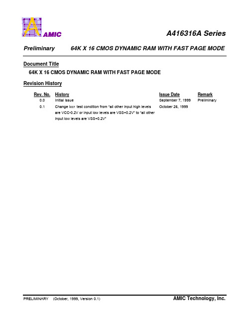
Preliminary
Document Title 64K X 16 CMOS DYNAMIC RAM WITH FAST PAGE MODE Revision History
Rev. No.
0.0 0.1
64K X 16 CMOS DYNAMIC RAM WITH FAST PAGE MODE
A0 – A7 I/O0 - I/O15
RAS
PRELIMINARY
A416316AS
(October, 1999, Version 0.1)
A416316AV
UCAS
LCAS
WE OE
VCC VSS NC
1
AMIC Technology, Inc.
元器件交易网
A416316A Series
RAS
UCAS
H L H
LCAS
H L L
WE
OE
Address L Row/Col. Row/Col.
I/Os L Data Out I/O0-7 = Data Out I/O8-15 = High-Z I/O0-7 = High-Z I/O8-15 = Data Out Data In I/O0-7 = Data In I/O8-15 = X I/O0-7 = X I/O8-15 = Data In Data Out → Data In Data Out Data Out Data In Data In Data In Data In Data Out Data In → High-Z High-Z X L
Preliminary
Features
n Organization: 65,536 words X 16 bits n Part Identification: - A416316A - A416316A-L (with self-refresh mode) n High speed - 30/35/40 ns RAS access time - 16/18/20 ns column address access time - 10/11/12 ns CAS access time n Low power consumption - Operating: 75mA (-30 max) - Standby: 3 mA (TTL) Separate CAS ( UCAS , LCAS ) for byte selection Self refresh mode 256 refresh cycles, 4 ms refresh interval Read-modify-write, RAS -only, CAS -before- RAS , Hidden refresh capability n TTL-compatible, three-state I/O n JEDEC standard packages - 400mil, 40-pin SOJ - 400mil, 40/44 TSOP type II package n Single 5V power supply/built-in VBB generator n n n n
CS5463A中文资料手册pdf
mcp73833 73834中文手册

0.10
58 47 25
100 1000
3000 300 300
100
3.7 3.6 —
4.232 4.382 4.433 4.533 0.30
0.30
— — —
110 1100
最大输出电流限制
IMAX
—
1200
—
µA 充电中
µA 充电结束
µA 待机 (没有接电池或 PROG 悬空)
MCP73833/4
独立线性锂离子 / 锂聚合物电池 充电管理控制器
特点
• 完整的线性充电管理控制器 - 内部集成了功率晶体管 - 内部集成了电流检测 - 内部集成了反向阻断保护
• 可进行热调节的恒流 / 恒压控制 • 高精度预置稳压:
- 4.2V, 4.35V, 4.4V 或 4.5V, +0.75% • 可编程充电电流:最大 1A • 对深度放电的电池进行预充
电流 + 限制 -
111 kΩ
+ - 预充
+ - 终止 + - 充电
+ CA 10 kΩ
470.6 kΩ 48 kΩ
+ VA -
充电控制 定时器 状态逻辑
VBAT
STAT1 STAT2 PG (TE)
DS22005A_CN 第 2 页
2007 Microchip Technology Inc.
MCP73833/4
晶体管导通电阻 导通电阻
VPTH / VREG VPHYS
ITERM / IREG
VRTH / VREG RDSON
— 64 69 —
3.75 5.6 7.5 15
AT738资料
90° 120°
180° DC
3000
4000
5000
IF(AV) [A]
PF(AV) [W] 7000 6000 5000
60° 90° 120° 180° DC
4000
30°
3000 2000 1000 0 0 1000 2000 3000 4000 5000 IF(AV) [A]
元器件交易网
AT738 PHASE CONTROL THYRISTOR
FINAL SPECIFICATION feb 97 - ISSUE : 02
ANSALDO
ON-STATE CHARACTERISTIC Tj = 125 °C 12000 60
SURGE CHARACTERISTIC Tj = 125 °C
Junction to heatsink, double side cooled Case to heatsink, double side cooled
11 2 -30 / 125 40.0 / 50.0 1700
°C/kW °C/kW °C kN g
VDRM&VRRM/100
元器件交易网
PHASE CONTROL THYRISTOR
AT738
Repetitive voltage up to Mean on-state current Surge current 2200 V 3670 A 60 kA
FINAL SPECIFICATION
feb 97 - ISSUE : 02
Symbol
2200 2300 2200 200 200
V V V mA mA
125 125
CONDUCTING
A43L2616AV-6中文资料

Preliminary 1M X 16 Bit X 4 Banks Synchronous DRAMDocument Title1M X 16 Bit X 4 Banks Synchronous DRAMRevision HistoryDate Remark Rev. No. History Issue issue November 30, 2004 Preliminary0.0 InitialA43L2616APreliminary1M X 16 Bit X 4 Banks Synchronous DRAMFeatureJEDEC standard 3.3V power supplyLVTTL compatible with multiplexed address Four banks / Pulse RAS MRS cycle with address key programs - CAS Latency (2,3)- Burst Length (1,2,4,8 & full page) - Burst Type (Sequential & Interleave) All inputs are sampled at the positive going edge of the system clock Clock Frequency: 166MHz @ CL=3 143MHz @ CL=3Burst Read Single-bit Write operationDQM for masking Auto & self refresh 64ms refresh period (4K cycle) Commercial Temperature Operation : 0°C~70°C Industrial Temperature Operation : -40°C~85°C for –U grade 54 Pin TSOP (II) and 54 Balls CSP (8mm x 8mm)General DescriptionThe A43L2616A is 67,108,864 bits synchronous high data rate Dynamic RAM organized as 4 X 1,048,576 words by 16 bits, fabricated with AMIC’s high performance CMOS technology. Synchronous design allows precise cycle control with the use of system clock.I/O transactions are possible on every clock cycle. Range of operating frequencies, programmable latencies allows the same device to be useful for a variety of high bandwidth, high performance memory system applications.Pin ConfigurationTSOP (II)V S SD Q 15V S S QD Q 14D Q 13V D D QD Q 12D Q 11V S S QD Q 10D Q 9V D D QD Q 8V S SU D Q MC KC K EN CA 9A 8A 7A 6A 5A 4V S SV D DD Q 0V D D QD Q 1D Q 2V S S QD Q 3D Q 4V D D QD Q 5D Q 6V S S QD Q 7V D DL D Q MW EC A SR A SC SA 10/A PB S 1B S 0A 0A 1A 2A 3V D DA 11N CPin Configuration (continued)54 Balls CSP (8 mm x 8 mm)Top ViewBlock DiagramCLKADDDQiPin DescriptionsAbsolute Maximum Ratings*Voltage on any pin relative to VSS (Vin, Vout ) . . . . . . . . .. . . . . . . . . . . . . . . . . . . . . . . . . . . . . . . . . . -1.0V to +4.6V Voltage on VDD supply relative to VSS (VDD, VDDQ ) . . . . . . . . . . . . . . . . . . . . . . . . . . . . . . . . . . .-1.0V to +4.6V Storage Temperature (T STG ) . . . . . . . . . . -55°C to +150°C Soldering Temperature X Time (T SLODER ) . . . . . . . . . . . . . . . . . . . . . . . . . . . . . . . . . . . . . . . . . . . . . . . . 260°C X 10sec Power Dissipation (P D ) . . . . . . . . . . . . . . . . . . . . . . . . .1W Short Circuit Current (Ios) . . . . . . . . . . . . . . . . . . . . 50mA *CommentsPermanent device damage may occur if “Absolute Maximum Ratings” are exceeded.Functional operation should be restricted to recommended operating condition.Exposure to higher than recommended voltage for extended periods of time could affect device reliability.Capacitance (T A =25°C, f=1MHz)DC Electrical CharacteristicsRecommend operating conditions (Voltage referenced to VSS = 0V, T A = 0ºC to +70ºC or T A = -40ºC to +85ºC)Parameter Symbol Min Typ Max Unit NoteSupply Voltage VDD,VDDQ 3.0 3.3 3.6 VInput High Voltage V IH 2.0 3.0 VDD+0.3 VInput Low Voltage V IL -0.3 0 0.8 V Note 1 Output High Voltage V OH 2.4 --V I OH = -2mAOutput Low Voltage V OL - - 0.4 V I OL = 2mA Input Leakage Current I IL -5 - 5 µA Note 2 Output Leakage Current I OL -5 - 5 µANote 3Output Loading ConditionSee Figure 1Note: 1. V IL (min) = -1.5V AC (pulse width ≤ 5ns).2. Any input 0V ≤ VIN ≤ VDD + 0.3V, all other pins are not under test = 0V3. Dout is disabled, 0V ≤ Vout ≤ VDDDecoupling Capacitance Guide LineRecommended decoupling capacitance added to power line at board.Parameter Symbol Value UnitDecoupling Capacitance between VDD and VSS C DC1 0.1 + 0.01 µF Decoupling Capacitance between VDDQ and VSSQC DC20.1 + 0.01µFNote: 1. VDD and VDDQ pins are separated each other.All VDD pins are connected in chip. All VDDQ pins are connected in chip. 2. VSS and VSSQ pins are separated each otherAll VSS pins are connected in chip. All VSSQ pins are connected in chip.DC Electrical Characteristics(Recommended operating condition unless otherwise noted, T A = 0°C to 70°C T A = -40ºC to +85ºC) Note: 1. Measured with outputs open. Addresses are changed only one time during t CC (min).2. Refresh period is 64ms. Addresses are changed only one time during t CC (min).3. I CC6 normal version: A43L2616AV-6, A43L2616AV-7.4. I CC6 low self refresh current version: A43L2616AV-6V, A43L2616AV-7V.AC Operating Test Conditions(VDD = 3.3V ±0.3V, T A = 0°C to +70°C or T A = -40ºC to +85ºC)Parameter ValueAC input levelsV IH /V IL = 2.4V/0.4V Input timing measurement reference level 1.4VInput rise and all time (See note3)tr/tf = 1ns/1ns Output timing measurement reference level 1.4V Output load conditionSee Fig.2Output(Fig. 1) DC Output Load Circuit ΩTT =1.4V (Fig. 2) AC Output Load CircuitAC Characteristics(AC operating conditions unless otherwise noted)-6 -7Symbol Parameter CAS Latency Min Max Min MaxUnit Notet CC CLK cycle time 6 1000 7 1000 ns 1t SACCLK to valid Output delay- 5 - 5.4 ns 1,2 t OH Output data hold time 2.5-2.7-ns2t CH CLK high pulse width 32.5 - 2.5 - ns 3 t CL CLK low pulse width 2.5 - 2.5 - ns 3 t SS Input setup time 2 - 2 - ns 3 t SH Input hold time 1 - 1 - ns 3 t SLZ CLK to output in Low-Z 1-1-ns2t SHZCLK to output In Hi-Z3- 5.5 - 6 ns*All AC parameters are measured from half to half.Note : 1. Parameters depend on programmed CAS latency.2. If clock rising time is longer than 1ns, (tr/2-0.5) ns should be added to the parameter.3. Assumed input rise and fall time (tr & tf) = 1ns.If tr & tf is longer than 1ns, transient time compensation should be considered, i.e., [(tr + tf)/2-1]ns should be added to the parameter.Operating AC Parameter(AC operating conditions unless otherwise noted)Note: 1. The minimum number of clock cycles is determined by dividing the minimum time required with clock cycle time and then rounding off to the next higher integer.2. Minimum delay is required to complete write.Simplified Truth Table(V = Valid, X = Don’t Care, H = Logic High, L = Logic Low) Note : 1. OP Code: Operand CodeA0~A11, BS0, BS1: Program keys. (@MRS)2. MRS can be issued only at both banks precharge state.A new command can be issued after 2 clock cycle of MRS.3. Auto refresh functions as same as CBR refresh of DRAM.The automatical precharge without Row precharge command is meant by “Auto”.Auto/Self refresh can be issued only at both precharge state.4. BS0, BS1 : Bank select address.If both BS1 and BS0 are “Low” at read, write, row active and precharge, bank A is selected.If both BS1 is “Low” and BS0 is “High” at read, write, row active and precharge, bank B is selected.If both BS1 is “High” and BS0 is “Low” at read, write, row active and precharge, bank C is selected.If both BS1 and BS0 are “High” at read, write, row active and precharge, bank D is selected.If A10/AP is “High” at row precharge, BS1 and BS0 is ignored and all banks are selected.5. During burst read or write with auto precharge, new read write command cannot be issued.Another bank read write command can be issued at every burst length.6. DQM sampled at positive going edge of a CLK masks the data-in at the very CLK (Write DQM latency is 0) butmasks the data-out Hi-Z state after 2 CLK cycles. (Read DQM latency is 2)Mode Register Filed Table to Program ModesRegister Programmed with MRS AddressBS0, BS1A11, A10A9A8A7A6A5A4A3A2A1A0FunctionRFURFU W.B.L TM CAS Latency BT Burst Length(Note 1)(Note 2)Test ModeCAS LatencyBurst TypeBurst LengthA8 A7TypeA6 A5 A4Latency A3TypeA2A1 A0 BT=0BT=10 0 Mode Register Set0 0 0Reserved0Sequential 00 0 1 1 0 1 0 0 1- 1Interleave 00 1 2 2 1 0 0 1 0 2 0 1 0 4 4 1 1Vendor Use Only0 1 1 3 0 1 188 Write Burst Length 1 0 0Reserved 10 0 Reserved Reserved A9 Length 1 0 1Reserved10 1 ReservedReserved0 Burst 1 1 0Reserved 1 1 0 Reserved Reserved 1 Single Bit 1 1 1Reserved11 1 256(Full)ReservedPower Up Sequence1. Apply power and start clock, Attempt to maintain CKE = “H”, DQM = “H” and the other pins are NOP condition at inputs.2. Maintain stable power, stable clock and NOP input condition for a minimum of 200µs.3. Issue precharge commands for all banks of the devices.4. Issue 2 or more auto-refresh commands.5. Issue a mode register set command to initialize the mode register. cf.) Sequence of 4 & 5 may be changed.The device is now ready for normal operation.Note : 1. RFU(Reserved for Future Use) should stay “0” during MRS cycle.2. If A9 is high during MRS cycle, “Burst Read Single Bit Write” function will be enabled.Burst Sequence (Burst Length = 4)Initial addressSequential Interleave A1 A00 0 0 1 2 3 0 1 2 30 1 1 2 3 0 1 0 3 21 023 0 1 2 3 0 11 1 3 0 123 2 1 0Burst Sequence (Burst Length = 8)Initial addressSequential Interleave A2 A1 A00 0 0 0 1 2 3 4 5 6 7 0 1 2 3 4 5 6 70 0 1 1 2 3 4 5 6 7 0 1 0 3 2 5 4 7 60 1 0 2 3 4 5 6 7 0 1 2 3 0 1 6 7 4 50 1 1 3 4 5 6 7 0 1 2 3 2 1 0 7 6 5 41 0 0 4 5 6 7 0 1234567 0 1 2 31 0 1 5 6 7 0 12345 4 76 1 0 3 21 1 0 6 7 0 1234567 4 5 2 3 0 11 1 1 7 0 1234567 6 5 4 3 2 1 0Device OperationsClock (CLK)The clock input is used as the reference for all SDRAM operations. All operations are synchronized to the positive going edge of the clock. The clock transitions must be monotonic between V IL and V IH. During operation with CKE high all inputs are assumed to be in valid state (low or high) for the duration of set up and hold time around positive edge of the clock for proper functionality and ICC specifications.Clock Enable (CLK)The clock enable (CKE) gates the clock onto SDRAM. If CKE goes low synchronously with clock (set-up and hold time same as other inputs), the internal clock is suspended form the next clock cycle and the state of output and burst address is frozen as long as the CKE remains low. All other inputs are ignored from the next clock cycle after CKE goes low. When both banks are in the idle state and CKE goes low synchronously with clock, the SDRAM enters the power down mode form the next clock cycle. The SDRAM remains in the power down mode ignoring the other inputs as long as CKE remains low. The power down exit is synchronous as the internal clock is suspended. When CKE goes high at least “t SS + 1 CLOCK” before the high going edge of the clock, then the SDRAM becomes active from the same clock edge accepting all the input commands.Bank Select (BS0, BS1)This SDRAM is organized as 4 independent banks of 1,048,576 words X 16 bits memory arrays. The BS0, BS1 inputs is latched at the time of assertion of RAS and CASto select the bank to be used for the operation. The bank select BS0, BS1 is latched at bank activate, read, write mode register set and precharge operations.Address Input (A0 ~ A11)The 20 address bits required to decode the 262,144 word locations are multiplexed into 12 address input pins (A0~A11). The 12 bit row address is latched along with RAS, BS0 and BS1 during bank activate command. The 8 bit column address is latched along with CAS, WE, BS0 and BS1during read or write command.NOP and Device DeselectWhen , CAS and WE are high, the SDRAM performs no operation (NOP). NOP does not initiate any new operation, but is needed to complete operations which require more than single clock like bank activate, burst read, auto refresh, etc. The device deselect is also a NOP and is entered by asserting CS high. CS high disables the command decoder so that RAS, CAS and WE, and all the address inputs are ignored.Power-UpThe following sequence is recommended for POWER UP 1. Power must be applied to either CKE and DQM inputs topull them high and other pins are NOP condition at the inputs before or along with VDD (and VDDQ) supply.The clock signal must also be asserted at the same time.2. After VDD reaches the desired voltage, a minimumpause of 200 microseconds is required with inputs in NOP condition.3. Both banks must be precharged now.4. Perform a minimum of 2 Auto refresh cycles to stabilizethe internal circuitry.5. Perform a MODE REGISTER SET cycle to program theCAS latency, burst length and burst type as the default value of mode register is undefined.At the end of one clock cycle from the mode register set cycle, the device is ready for operation.When the above sequence is used for Power-up, all the out-puts will be in high impedance state. The high impedance of outputs is not guaranteed in any other power-up sequence.cf.) Sequence of 4 & 5 may be changed.Mode Register Set (MRS)The mode register stores the data for controlling the various operation modes of SDRAM. It programs the CAS latency, addressing mode, burst length, test mode and various vendor specific options to make SDRAM useful for variety of different applications. The default value of the mode register is not defined, therefore the mode register must be written after power up to operate the SDRAM. The mode register is written by asserting low on CS,RAS, CAS,(The SDRAM should be in active mode with CKE already high prior to writing the mode register). The state of address pins A0~A11, BS0 and BS1 in the same cycle as CS,,CAS,WE going low is the data written in the mode register. One clock cycle is required to complete the write in the mode register. The mode register contents can be changed using the same command and clock cycle requirements during operation as long as both banks are in the idle state. The mode register is divided into various fields depending on functionality. The burst length field uses A0~A2, burst type uses A3, addressing mode uses A4~A6, A7~A8, A11, BS0 and BS1 are used for vendor specific options or test mode. And the write burst length is programmed using A9. A7~A8, A11, BS0 and BS1 must be set to low for normal SDRAM operation.Refer to table for specific codes for various burst length, addressing modes and CAS latencies.Device Operations (continued)Bank ActivateThe bank activate command is used to select a random row in an idle bank. By asserting low on RAS and CS with desired row and bank addresses, a row access is initiated. The read or write operation can occur after a time delay of t RCD(min) from the time of bank activation. t RCD(min) is an internal timing parameter of SDRAM, therefore it is dependent on operating clock frequency. The minimum number of clock cycles required between bank activate and read or write command should be calculated by dividing t RCD(min) with cycle time of the clock and then rounding off the result to the next higher integer. The SDRAM has two internal banks on the same chip and shares part of the internal circuitry to reduce chip area, therefore it restricts the activation of both banks immediately. Also the noise generated during sensing of each bank of SDRAM is high requiring some time for power supplies recover before the other bank can be sensed reliably. t RRD(min) specifies the minimum time required between activating different banks. The number of clock cycles required between different bank activation must be calculated similar to t RCD specification. The minimum time required for the bank to be active to initiate sensing and restoring the complete row of dynamic cells is determined by t RAS(min) specification before a precharge command to that active bank can be asserted. The maximum time any bank can be in the active state is determined by t RAS(max). The number of cycles for both t RAS(min) and t RAS(max) can be calculated similar to t RCD specification.Burst ReadThe burst read command is used to access burst of data on consecutive clock cycles from an active row in an active bank. The burst read command is issued by asserting low on CS and CAS with WE being high on the positive edge of the clock. The bank must be active for at least t RCD(min) before the burst read command is issued. The first output appears CAS latency number of clock cycles after the issue of burst read command. The burst length, burst sequence and latency from the burst read command is determined by the mode register which is already programmed. The burst read can be initiated on any column address of the active row. The address wraps around if the initial address does not start from a boundary such that number of outputs from each I/O are equal to the burst length programmed in the mode register. The output goes into high-impedance at the end of the burst, unless a new burst read was initiated to keep the data output gapless. The burst read can be terminated by issuing another burst read or burst write in the same bank or the other active bank or a precharge command to the same bank. The burst stop command is valid at every page burst length. Burst WriteThe burst write command is similar to burst read command, and is used to write data into the SDRAM consecutive clock cycles in adjacent addresses depending on burst length and burst sequence. By asserting low on CS,CAS and WE with valid column address, a write burst is initiated. The data inputs are provided for the initial address in the same clock cycle as the burst write command. The input buffer is deselected at the end of the burst length, even though the internal writing may not have been completed yet. The writing can not complete to burst length. The burst write can be terminated by issuing a burst read and DQM for blocking data inputs or burst write in the same or the other active bank. The burst stop command is valid only at full page burst length where the writing continues at the end of burst and the burst is wrap around. The write burst can also be terminated by using DQM for blocking data and precharging the bank “t RDL” after the last data input to be written into the active row. See DQM OPERATION also.DQM OperationThe DQM is used to mask input and output operation. It works similar to OE during read operation and inhibits writing during write operation. The read latency is two cycles from DQM and zero cycle for write, which means DQM masking occurs two cycles later in the read cycle and occurs in the same cycle during write cycle. DQM operation is synchronous with the clock, therefore the masking occurs for a complete cycle. The DQM signal is important during burst interrupts of write with read or precharge in the SDRAM. Due to asynchronous nature of the internal write, the DQM operation is critical to avoid unwanted or incomplete writes when the complete burst write is not required.PrechargeThe precharge operation is performed on an active bank by asserting low on CS,RAS,WE and A10/AP with valid BA of the bank to be precharged. The precharge command can be asserted anytime after t RAS(min) is satisfied from the bank activate command in the desired bank. “t RP” is defined as the minimum time required to precharge a bank. The minimum number of clock cycles required to complete row precharge is calculated by dividing “t RP” with clock cycle time and rounding up to the next higher integer. Care should be taken to make sure that burst write is completed or DQM is used to inhibit writing before precharge command is asserted. The maximum time any bank can be active is specified by t RAS(max). Therefore, each bank has to be precharged within t RAS(max) from the bank activate command. At the end of precharge, the bank enters the idle state and is ready to be activated again.Entry to Power Down, Auto refresh, Self refresh and Mode register Set etc, is possible only when both banks are in idle state.Device Operations (continued)Auto PrechargeThe precharge operation can also be performed by usingauto precharge. The SDRAM internally generates thetiming to satisfy t RAS(min) and “t RP” for the programmedburst length and CAS latency. The auto prechargecommand is issued at the same time as burst read or burstwrite by asserting high on A10/AP. If burst read or burstwrite command is issued with low on A10/AP, the bank isleft active until a new command is asserted. Once autoprecharge command is given, no new commands arepossible to that particular bank until the bank achieves idlestate.Four Banks PrechargeBoth banks can be precharged at the same time by using Precharge all command. Asserting low on CS,RAS and WE with high on A10/AP after both banks have satisfied t RAS(min) requirement, performs precharge on both banks.At the end of tRP after performing precharge all, bothbanks are in idle state.Auto RefreshThe storage cells of SDRAM need to be refreshed every64ms to maintain data. An auto refresh cycle accomplishesrefresh of a single row of storage cells. The internalcounter increments automatically on every auto refreshcycle to refresh all the rows. An auto refresh command is issued by asserting low on CS,RAS and CAS with high on CKE and WE. The auto refresh command can only be asserted with both banks being in idle state and the deviceis not in power down mode (CKE is high in the previouscycle). The time required to complete the auto refresh operation is specified by “t RC(min)”. The minimum number of clock cycles required can be calculated by driving “t RC” with clock cycle time and then rounding up to the next higher integer. The auto refresh command must be followed by NOP’s until the auto refresh operation is completed. Both banks will be in the idle state at the end of auto refresh operation. The auto refresh is the preferred refresh mode when the SDRAM is being used for normal data transactions. The auto refresh cycle can be performed once in 15.6us or a burst of 4096 auto refresh cycles once in 64ms.Self RefreshThe self refresh is another refresh mode available in the SDRAM. The self refresh is the preferred refresh mode for data retention and low power operation of SDRAM. In self refresh mode, the SDRAM disables the internal clock and all the input buffers except CKE. The refresh addressing and timing is internally generated to reduce power consumption.The self refresh mode is entered from all banks idle state by asserting low on CS,RAS,CAS and CKE with high on WE. Once the self refresh mode is entered, only CKE state being low matters, all the other inputs including clock are ignored to remain in the self refresh.The self refresh is exited by restarting the external clock and then asserting high on CKE. This must be followed by NOP’s for a minimum time of “t RC” before the SDRAM reaches idle state to begin normal operation. If the system uses burst auto refresh during normal operation, it is recommended to used burst 4096 auto refresh cycles immediately after exiting self refresh.Basic feature And Function Descriptions1. CLOCK SuspendNote: CLK to CLK disable/enable=1 clock2. DQM Operation* Note : 1. DQM makes data out Hi-Z after 2 clocks which should masked by CKE “L”.2. DQM masks both data-in and data-out.3. CAS Interrupt (I)Note : 1. By “Interrupt”, It is possible to stop burst read/write by external command before the end of burst.By “CAS Interrupt”, to stop burst read/write by CAS access; read, write and block write.2. t CCD : CAS to CAS delay. (=1CLK)3. t CDL : Last data in to new column address delay. (= 1CLK).4. CAS Interrupt (II) : Read Interrupted Write & DQM* Note : 1. To prevent bus contention, there should be at least one gap between data in and data out.2. To prevent bus contention, DQM should be issued which makes a least one gap between data in and data out.5. Write Interrupted by Precharge & DQMNote : 1. To inhibit invalid write, DQM should be issued.2. This precharge command and burst write command should be of the same bank, otherwise it is not prechargeinterrupt but only another bank precharge of dual banks operation.6. Precharge7. Auto Precharge* Note : 1. The row active command of the precharge bank can be issued after t RP from this point.The new read/write command of other active bank can be issued from this point.At burst read/write with auto precharge, CAS interrupt of the same/another bank is illegal.8. Burst Stop & Interrupted by Precharge9. MRSNote : 1. t RDL : 1CLK 2. t BDL : 1CLK; Last data in to burst stop delay.Read or write burst stop command is valid at every burst length.3. Number of valid output data after row precharge or burst stop: 1,2 for CAS latency = 2, 3 respectively.4. PRE: All banks precharge if necessary.MRS can be issued only when all banks are in precharged state.10. Clock Suspend Exit & Power Down Exit11. Auto Refresh & Self Refresh* Note : 1. Active power down : one or more bank active state.2. Precharge power down : both bank precharge state.3. The auto refresh is the same as CBR refresh of conventional DRAM.No precharge commands are required after Auto Refresh command.During t RC from auto refresh command, any other command can not be accepted.4. Before executing auto/self refresh command, both banks must be idle state.5. MRS, Bank Active, Auto/Self Refresh, Power Down Mode Entry.6. During self refresh mode, refresh interval and refresh operation are performed internally.After self refresh entry, self refresh mode is kept while CKE is LOW.During self refresh mode, all inputs expect CKE will be don’t cared, and outputs will be in Hi-Z state.During t RC from self refresh exit command, any other command can not be accepted.Before/After self refresh mode, burst auto refresh cycle (4K cycles ) is recommended.12. About Burst Type ControlSequential counting At MRS A3=”0”. See the BURST SEQUENCE TABE.(BL=4,8) BL=1,2,4,8 and full page wrap around.BasicMODEInterleave counting At MRS A3=” 1”. See the BURST SEQUENCE TABE.(BL=4,8) BL=4,8 At BL=1,2 Interleave Counting = Sequential CountingRandom MODE Random column Accesst CCD = 1 CLKEvery cycle Read/Write Command with random column address can realizeRandom Column Access.That is similar to Extended Data Out (EDO) Operation of convention DRAM.13. About Burst Length ControlPower On Sequence & Auto RefreshCKECSRASCASADDRBS0, BS1A10/APWEDQMDQ(A-Bank)Single Bit Read-Write-Read Cycles (Same Page) @CAS Latency=3, Burst Length=1CLOCKCKECSRASCASADDRBS0, BS1A10/APWEDQMDQ* Note : 1. All inputs can be don’t care when CS is high at the CLK high going edge.2. Bank active & read/write are controlled by BS0, BS1.BS1 BS0 Active & Read/WriteA0 0 BankB0 1 BankC1 0 BankD1 1 Bank3. Enable and disable auto precharge function are controlled by A10/AP in read/write command.A10/AP BS1 BS0Operation0 0 Disable auto precharge, leave bank A active at end of burst.0 1 Disable auto precharge, leave bank B active at end of burst.1 0 Disable auto precharge, leave bank C active at end of burst.1 1 Disable auto precharge, leave bank D active at end of burst.0 0 Enable auto precharge, precharge bank A at end of burst.0 1 Enable auto precharge, precharge bank B at end of burst.11 0 Enable auto precharge, precharge bank C at end of burst.1 1 Enable auto precharge, precharge bank D at end of burst.4. A10/AP and BS0, BS1 control bank precharge when precharge command is asserted.A10/AP BS1 BS0 PrechargeA0 0 0 BankB0 0 1 BankC0 1 0 BankD0 1 1 BankBanks1 X X All。
BYV36A中文资料
current
IF = 1 A to VR ≥ 30 V and
BYV36A to C
dIF/dt = −1 A/µs;
see Fig.27
BYV36D and E
BYV36F and G
MIN.
− − −
− − −
− − −
TYP. MAX. UNIT
−
100 ns
−
150 ns
−
250 ns
45
Product specification
BYV36 series
SYMBOL
PARAMETER
CONDITIONS
trr
reverse recovery time
BYV36A to C
BYV36D and E
BYV36F and G
when switched from
IF = 0.5 A to IR = 1 A; measured at IR = 0.25 A; see Fig. 26
元器件交易网
DISCRETE SEMICONDUCTORS
DATA SHEET
handbook, 2 columns
M3D116
BYV36 series Fast soft-recovery controlled avalanche rectifiers
Product specification Supersedes data of 1996 May 30
Fig.4 Maximum average forward current as a function of tie-point temperature (including losses due to reverse leakage).
TLP3526中文资料

1.0
1.4
1.8
2.2
2.6
Pulse forward voltage VFP (V)
4
2002-09-25
元器件交易网
Trigger LED current IFT (arbitrary unit)
Peak off-state current IDRM (arbitrary unit)
元器件交易网
TL(Ta = 25°C)
Characteristic
Symbol
Rating
Unit
Forward current
Forward current derating (Ta ≥ 53°C)
LE D
Peak forward current (100µs pulse, 100pps)
Characteristic Trigger LED current Capacitance (input to output) Isolation resistance
Isolation voltage
Fig.1: dv / dt test circuit
Symbol IFT CS RS
BVS
Test Condition
VT = 6V VS = 0, f = 1MHz VS = 500V AC, 1 minute AC, 1 second, in oil DC, 1 minute, in oil
Min.
―
― 5×10¹⁰ 2500
― ―
Typ.
―
1.5 1014 ― 5000 5000
Max. 10 ―
― ― ― ―
1 5 125 600 1.0 0.7 -14.3
A3361中文资料
A3361中文资料The A3361x and A3362x Hall-effect switches are extremely temperature-stable and stress-resistant sensors. Superior performance over temperature is made possible through dynamic offset cancellation,which reduces the residual offset voltage normally caused by device overmolding, temperature dependencies, and thermal stress. The two devices differ only in output polarity; the A3361x output current goes low in the presence of a south pole of sufficient strength; the A3362x output current goes high.Each device includes on a single silicon chip a voltage regulator,Hall-voltage generator, small-signal amplifier, chopper stabilization,Schmitt trigger, and a constant-current open-collector output. An on-board regulator permits operation with supply voltages of 3.5 to 24volts. Noise radiation is limited by control of the output current slew rate.Three package styles provide a magnetically optimized package for most applications. Su ffix ‘xLH’ is a miniature low-profile surface-mount package, ‘xLT’ is a miniature SOT-89/TO-243AA transistor package for surface-mount applications; while suffix ‘xUA’ is a three-lead ultra-mini-SIP for through-hole mounting.FEATURESs Internal Current Regulator for 2-Wire Operation s Resistant to Physical Stress s Superior Temperature Stability s Operation From Unregulated Supply s Solid-State Reliability s Small Size Always order by complete part number: the prefix 'A' + the basic four-digitpart number + a suffix to indicate operating temperature range (E) +a two-letter suffix to indicate package style, e.g., A3361ELH .2-WIRE, CHOPPER-STABILIZED,HALL-EFFECT SWITCHES3361 AND 3362Data Sheet 27621.503361 AND 33622-WIRE,CHOPPER-STABILIZED,HALL-EFFECT SWITCHES115 Northeast Cutoff, Box 15036Worcester, Massachusetts 01615-0036 (508) 853-50002Copyright ? 2001 Allegro MicroSystems, Inc.Pinning is shown viewed from branded side.Dwg. PH-003-6S U P P L YG R O U N DN O (I N T E R N A L )C O N N E C T I O NDwg. PH-003-7A S U P P L YG R O U N DG R O U N DSuffix Code 'UA' Pinning(SIP)Suffix Code 'LT' Pinning (SOT-89/TO-243AA)3361 AND 33622-WIRE,CHOPPER-STABILIZED,HALL-EFFECT SWITCHES/doc/1377bc3d67ec102de2bd8931.ht ml3A3361 MAGNETIC CHARACTERISTICS over operating supply voltage and temperature ranges.LimitsCharacteristic Symbol Test Conditions Min.Typ.Max.Units Operate Point B OP B > B OP , I GND = LOW ––125G Release Point B RP B < B RP , I GND = HIGH 40––G HysteresisB hysB OP - B RP5.0–30GA3362 MAGNETIC CHARACTERISTICS over operating supply voltage and temperature ranges.LimitsCharacteristic Symbol Test Conditions Min.Typ.Max.Units Operate Point B OP B > B OP , I GND = HIGH ––125G Release Point B RP B < B RP , I GND = LOW 40––G HysteresisB hysB OP - B RP5.0–30GELECTRICAL CHARACTERISTICS over operating temperature range.LimitsCharacteristic Symbol Test Conditions Min.Typ.Max.Units Supply Voltage V CC Operating3.51224V Output CurrentI GND(L)Output Current Low 5.0– 6.9mA I GND(H)Output Current High12–17mA Chopping Frequency f C –340–kHz Output Settling Time t sd C L = 20 pF ––50μs Output Rise Time t r C L = 20 pF –3.5–μs Output Fall Time t f C L = 20 pF – 3.5–μs Reverse Battery CurrentI CCV RCC = -16 V ––-15mANOTE:Typical Data is at T A = +25°C and V CC = 12 V and is for design information only.3361 AND 33622-WIRE,CHOPPER-STABILIZED,HALL-EFFECT SWITCHES115 Northeast Cutoff, Box 15036Worcester, Massachusetts 01615-0036 (508) 853-5000 4O U T P U T C U R R E N TFLUX DENSITYDwg. GH-007-3+IOUTPUT CHARACTERISTICSA3361xA3362x+B0O U T P U T C U R R E N TFLUX DENSITYDwg. GH-007-4RP B OP B I OUT + I CC I CC +I3361 AND 33622-WIRE,CHOPPER-STABILIZED,HALL-EFFECT SWITCHES/doc/1377bc3d67ec102de2bd8931.ht ml5SENSOR LOCATIONS(±0.005” [0.13 mm] die placement)Package Designator “LH”Package Designators “UA” and "UA-TL"Although sensor location is accurate to three sigma for a particular design, product improvements may result in small changes to sensor location.0.011"0.28 mm NOMDwg. MH-008-8A0.0305"0.775 mm NOMACTIVE AREA DEPTHDwg. MH-011-9BPackage Designator “LT”60040020020601001400AMBIENT TEMPERATURE in °CA L L O W AB L E P AC K A G EP O W E R D I S S I P A T I O N i n M I L L I W A T T SDwg. GH-046-440801201807005003001001603361 AND 33622-WIRE,CHOPPER-STABILIZED,HALL-EFFECT SWITCHES115 Northeast Cutoff, Box 15036Worcester, Massachusetts 01615-0036 (508) 853-50006All Allegro sensors are subjected to stringent qualification requirements prior to being released to production.To become qualified, except for the destructive ESD tests, no failures are permitted.CRITERIA FOR DEVICE QUALIFICATIONQualification Test Test Method and Test Conditions Test Length SamplesComments Biased Humidity (HAST)T A = 130°C, RH = 85%50 hrs 77V CC = V OUT = 5 V High-Temperature JESD22-A108, 408 hrs77V CC = 24 V,Operating Life (HTOL)T A = 150°C, T J = 165°C VOUT = 20 V Accelerated HTOLJESD22-A108,504 hrs 77V CC = 24 V,T A = 175°C, T J = 190°C V OUT = 20 VAutoclave, Unbiased JESD22-A102, Condition C,96 hrs 77T A = 121°C, 15 psig High-Temperature MIL-STD-883, Method 1008,1000 hrs 77(Bake) Storage Life T A = 170°CTemperature CycleMIL-STD-883, Method 1010,500 cycles 77-65°C to +150°C Latch-Up—Pre/Post 6Reading Electro-Thermally—Pre/Post 6Induced Gate Leakage Reading ESD,CDF-AEC-Q100-002Pre/Post x per Test to failure,Human Body Model Reading test All leads > TBDElectrical DistributionsPer Specification—303361 AND 33622-WIRE,CHOPPER-STABILIZED,HALL-EFFECT SWITCHES/doc/1377bc3d67ec102de2bd8931.ht ml7FUNCTIONAL DESCRIPTION+—Dwg. AH-011-2Chopper-Stabilized Technique. The Hall element can be considered as a resistor array similar to a Wheatstone bridge. A large portion of the offset is a result of the mismatching of these resistors. These devices use a proprietary dynamic offset cancellation technique, with an internal high-frequency clock to reduce the residual offset voltage of the Hall element that is normally caused by device overmolding, temperature dependen-cies, and thermal stress. The chopper-stabilizing technique cancels the mismatching of the resistor circuit by changing the direction of the current flowing through the Hall plate using CMOS switches and Hall voltage measurement taps, while maintaing the Hall-voltage signal that is induced by the external magnetic flux. The signal is then captured by a sample-and-hold circuit and further processed using low-offset bipolar circuitry. This technique produces devices that have an extremely stable quiescent Hall output voltage, are immune to thermal stress, and have precise recoverability after temperature cycling. This technique will also slightly degrade the device output repeatability. A relatively high sampling frequency is used in order that faster signals can be processed.More detailed descriptions of the circuit operation can be found in: Technical Paper STP 97-10, Monolithic Magnetic Hall Sensor Using Dynamic Quadrature Offset Cancellation andTechnical Paper STP 99-1, Chopper-Stabilized Amplifiers With A Track-and-Hold Signal Demodulator .Operation. As shown in the output characteristic graphs, the output of the A3362 turns on when a magnetic field (south pole)perpendicular to the Hall sensor is increased above the operate point threshold (B OP ). After turn on, the output will source current equal to the device operating current plus a current source (I GND(H)). When the magnetic field is decreased below the release point (B RP ), the output turns off and will source current equal only to the Hall-effect sensor operating current (I GND(L)). The A3361 output is inverted and the device turns off at B OP and on at B RP . The difference in the magnetic operate and release points is the hysteresis (B hys ) of the device. The hysteresis allows clean switching of the output even in the presence of external mechanical vibration or electrical noise.Applications. It is strongly recommended that an external bypass capacitor be connected (in close proximity to the Hall sensor) between the supply and ground of the device to reduce both external noise and noise generated by the chopper-stabilization technique.Extensive applications information on magnets and Hall-effect sensors is also available in the Allegro Electronic Data Book AMS-702 or Application Note 27701 or/doc/1377bc3d67ec102de2bd8931.ht ml3361 AND 33622-WIRE,CHOPPER-STABILIZED,HALL-EFFECT SWITCHES115 Northeast Cutoff, Box 15036Worcester, Massachusetts 01615-0036 (508) 853-50008PACKAGE DESIGNATOR 'LH'(fits SC-74A solder-pad layout)NOTES: 1.Tolerances on package height and width represent allowable mold offsets. Dimensions given are measured at the widest point (parting line).2.Exact body and lead configuration at vendor’s option within limits shown.3.Height does not include mold gate flash.4.Where no tolerance is specified, dimension is nominal.Dwg. MA-011-3 mmDwg. MA-010-3C in0.00790.00500° GAUGE PLANEDwg. MA-011-3 inDimensions in Inches (for reference only)Dimensions in Millimeters(controlling dimensions)Dwg. MA-010-3C mm0.200.1270° GAUGE PLANE3361 AND 33622-WIRE,CHOPPER-STABILIZED,HALL-EFFECT SWITCHES/doc/1377bc3d67ec102de2bd8931.ht ml90.440.35PACKAGE DESIGNATOR 'LT'(SOT-89/TO-243AA)Dimensions in Inches (for reference only)Dimensions in Millimeters (controlling dimensions)Dwg. MA-012-3 mmPads 1, 2, 3, and B — Low-Stress VersionPads 1, 2, and 3 only — Lowest Stress, But Not Self Aligning NOTE: Exact body and lead configuration at vendor’s option within limits shown.Dwg. MA-012-3 inds 1, 2, 3, and A — Standard SOT-89 Layout ds 1, 2, 3, and B — Low-Stress Versionds 1, 2, and 3 only — Lowest Stress, But Not Self Aligning3361 AND 33622-WIRE,CHOPPER-STABILIZED,HALL-EFFECT SWITCHES115 Northeast Cutoff, Box 15036Worcester, Massachusetts 01615-0036 (508) 853-500010Surface-Mount Lead Form (order A336xEUA-TL)Dimensions in Inches (controlling dimensions)Dimensions in Millimeters(for reference only)PACKAGE DESIGNATOR 'UA'Dwg. MH-014E mm1.27BSC°Dwg. MH-014E in0.050BSC°NOTES: 1.Tolerances on package height and width represent allowable mold offsets. Dimensions given are measured at the widest point (parting line).2.Exact body and lead configuration at vendor’s optionwithin limits shown.3.Height does not include mold gate flash.4.Recommended minimum PWB hole diameter to clear transition area is 0.035” (0.89 mm).5.Where no tolerance is specified, dimension is nominal.3361 AND 33622-WIRE,CHOPPER-STABILIZED,HALL-EFFECT SWITCHES/doc/1377bc3d67ec102de2bd8931.ht ml11The products described herein are manufactured under one or more of the following U.S. patents: 5,045,920; 5,264,783; 5,442,283;5,389,889; 5,581,179; 5,517,112; 5,619,137; 5,621,319; 5,650,719;5,686,894; 5,694,038; 5,729,130; 5,917,320; and other patents pending.Allegro MicroSystems, Inc. reserves the right to make, from time to time, such departures from the detail specifications as may berequired to permit improvements in the performance, reliability, or manufacturability of its products. Before placing an order, the user is cautioned to verify that the information being relied upon is current.Allegro products are not authorized for use as critical components in life-support appliances, devices, or systems without express written approval.The information included herein is believed to be accurate and reliable. However, Allegro MicroSystems, Inc. assumes no responsi-bility for its use; nor for any infringements of patents or other rights of third parties that may result from its use.3361 AND 33622-WIRE,CHOPPER-STABILIZED,HALL-EFFECT SWITCHES115 Northeast Cutoff, Box 15036Worcester, Massachusetts 01615-0036 (508) 853-500012HALL-EFFECT SENSORSPartial Part Avail. Oper.Characteristics at T A = +25°C Number Temp.B OP max B RP min B hys typ Features NotesHALL-EFFECT UNIPOLAR & OMNIPOLAR SWITCHES in order of B OP and B hys 3240E/L +50+5.010chopper stabilized 13209E ±60±5.07.7400 μW, chopper stabilized 3210E ±60±5.07.725 μW, chopper stabilized3361E +125+40 5.0*2-wire, chopper stabilized, inverted output 3362E +125+40 5.0*2-wire, chopper stabilized 3161E +160+30202-wire3141E/L +160+10553235S +175+2515*output 12-25-17515*output 225140E +200+5055300 mA power driver output13142E/L +230+75553143E/L +340+165553144E/L +350+50553122E/L +400+1401053123E/L +440+1801053121 E/L+450+125105HALL-EFFECT LATCHES & BIPOLAR SWITCHES ?in order of B OP and B hys3260E/L +30-3020bipolar switch, chopper stabilized 3425L+30-3019dual bipolar switch, stabilized 13280E/L +40-4045chopper stabilized 3134E/L +50-5027bipolar switch 3133K/L/S +75-7552bipolar switch 3281E/L +90-90100chopper stabilized 3132K/L/S +95-9552bipolar switch 3187E/L +150-150100*3177S +150-1502003195E/L +160-160220active pulldown 13197L +160-16023013175S +170-1702003188E/L +180-180200*3283E/L +180-180300chopper stabilized 3189E/L +230-230100*3275S +250-250100*33185E/L +270-270340*Operating Temperature Ranges:S = -20°C to +85°C, E = -40°C to +85°C, J = -40°C to +115°C, K = -40°C to +125°C, L = -40°C to +150°CNotes 1.Protected.2.Output 1 switches on south pole, output 2 switches on north pole for 2-phase, bifilar-wound, unipolar-driven brushless dc motor control. Outputs may be tied together for omnipolar operation./doc/1377bc3d67ec102de2bd8931.ht ml plementary outputs for 2-phase bifilar-wound, unipolar-driven brushless dc motor control.*Minimum. ? MaximumLatches will not switch on removal of magnetic field; bipolar switches may switch on removal of field but require field reversal for reliable operation over operating temperature range.。
L8506资料
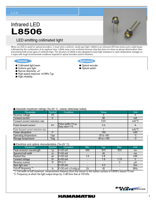
Germany: Hamamatsu Photonics Deutschland GmbH: Arzbergerstr. 10, D-82211 Herrsching am Ammersee, Germany, Telephone: (49) 08152-3750, Fax: (49) 08152-2658
+1
0
-1
-2
-3
0
20
40
60
80
100
AMBIENT TEMPERATURE (˚C)
KLEDB0228EA
s Relative light intensity distribution
100 L=5 mm
80
L=10 mm
60
L=20 mm
RELATIVE RADIANT OUTPUT (%)
Pulse forward current
IFP
Pulse width=10 µs Duty ratio=1 %
Pulse forward current reduction rate
-
Power dissipation
P
Operating temperature
Topr
Storage temperature
LED
Infrared LED
L8506
LED emitting collimated light
When an LED is used for optical encoders, it must emit a uniform, small spot light. L8506 is an infrared LED that emits such a light beam collimated by the combination of an aspheric lens. L8506 uses a non-confined structure chip that does not show an abrupt deterioration often encountered with some types of confined chips. The structure of L8506 is also designed to have high resistance to cyclic temperature changes so it copes with tough environmental conditions required for optical encoders used in factories.
- 1、下载文档前请自行甄别文档内容的完整性,平台不提供额外的编辑、内容补充、找答案等附加服务。
- 2、"仅部分预览"的文档,不可在线预览部分如存在完整性等问题,可反馈申请退款(可完整预览的文档不适用该条件!)。
- 3、如文档侵犯您的权益,请联系客服反馈,我们会尽快为您处理(人工客服工作时间:9:00-18:30)。
18
Telephone: 781-935-4442 Fax: 781-938-5867
sales@ Engineering Catalog 169
Telephone: 781-935-4442 Fax: 781-938-5867
sales@ Engineering Catalog 169 17
元器件交易网
A
Quartz Halogen Projection Lamps
B
Quartz Halogen Lamps
Line No. Color Temp. Part Reference Degrees No. No. Volts Watts Lumens Kelvin Hours 3,000 3,000 3,000 3,000 3,400 3,400 2,000 2,000 2,000 2,000 50 50 Life Position Any Any * * * * Burning Type C-Bar-6 C-6 C-6 C-6 C-Bar 6 C-Bar 6 Filament Filament Dimensions Lgth. x Dia. D MOL LCL 4.2 x 2.5 4.2 x 1.5 5.0 x 1.8 5.2 x 2.28 5.3 x 3.0 6.2 x 3.1 11.0 11.0 11.0 11.0 11.0 13.5 44.0 44.0 44.0 44.0 44.0 50.0 30.0 30.0±0.25 30.0±0.25 30.0±0.25 30.0±0.25 32.0±0.5 Type Base Drawing B B B B B B 13 L7417 —12.0 50 900 14 L7389A —12.0 50 900 15 L7386A —12.0 75 1,400 16 L7390A —12.0 100 2,000 17 L7407 FCR 12.0 100 3,000 18 L6405 FCS 24.0 150 4,700 Recommended Holders/Sockets Pages 32 & 33 GY6.35 GY6.35 GY6.35 GY6.35ion Quartz Halogen Lamps, Prefocused Filaments
Line No. Part No. Volts Color Temp. Degrees Watts Lumens Kelvin Life Hours Filament Burning Filament Dimensions Position Type Lgth. x Dia. D Dimensions MOL LCL 55.0 60.0 60.0 30.3±0.25 33.3±0.25 33.3±0.25 Base Type GY9.5 GY9.5 GY9.5 Dwg B C D 7 L9404 12.0 20 300 2,700 2,000 Any C-6 3.24 x 0.92 8 L9389 12.0 50 900 3,000 2,000 Any C-6 4.50 x1.64 9 L9390 12.0 100 2,400 2,990 2,000 * C-Bar 6 5.50 x 3.00 *Base Down to Horizontal, Cooling Required L9390 Only. Recommended Holders/Sockets Page 35 11.0 12.0 11.0
元器件交易网
A
Miniature Quartz Halogen Lamps
Line No. Part No. Volts Color Temp. Degrees Watts Lumens Kelvin 3,150 2,850 2,950 3,200 3,000 2,800 2,900 2,850 3,150 3,000 2,850 2,900 Life Hours 100 2,000 1,000 100 2,000 2,000 1,000 1,000 250 2,000 2,000 2,000 Burning Filament Filament Position Type Lgth. x Dia. Any Any Any Any Any Any Any Any Any Any Any Any C-6 C-6 C-6 C-6 C-6 C-6 C-6 C-6 C-6 C-6 C-6 C-6 2.5 3.0 2.8 2.1 2.9 3.4 3.8 4.25 2.6 3.3 4.0 4.8 0.6 0.7 0.6 1.0 1.0 0.7 0.7 0.35 1.0 0.9 0.7 1.1 D 9.0 9.0 9.0 9.0 9.0 9.0 9.0 9.0 9.0 9.0 9.0 9.0 Dimensions MOL LCL 30.0 30.0 30.0 30.0 30.0 30.0 30.0 30.0 30.0 30.0 30.0 30.0 19.5±0.25 19.5±0.25 19.5±0.25 19.5±0.25 19.5±0.25 19.5±0.25 19.5±0.25 18.75±0.25 19.5±0.25 19.5±0.25 19.5±0.25 19.5±0.25 Base Type Drawing G-4 G-4 G-4 G-4 G-4 G-4 G-4 G-4 G-4 G-4 G-4 G-4 A A A A A A A A A A A A 1 L7387 6.0 10 180 2 L6402 6.0 10 130 3 L6414 6.0 10 150 4 L7388 6.0 20 420 5 L7394 6.0 20 350 6 L6415 12.0 10 120 7 L6416 12.0 15 210 8 L6417 12.0 10 130 9 L7401 12.0 20 420 10 L7404 12.0 20 350 11 L7404A 12.0 20 280 12 L7414A 12.0 35 560 Recommended Holders/Sockets Pages 28 & 29