03_timing_adders
8313配置文件及说明
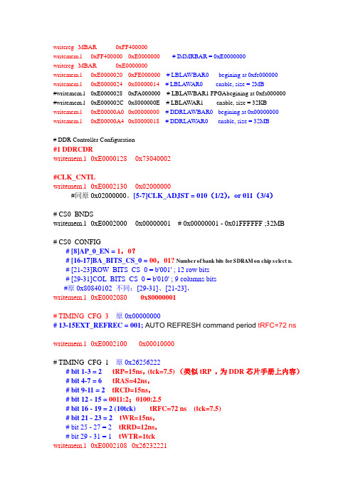
writereg MBAR 0xFF400000writemem.l 0xFF400000 0xE0000000 # IMMRBAR = 0xE0000000writereg MBAR 0xE0000000writemem.l 0xE0000020 0xFE000000# LBLAWBAR0 - begining at 0xfe000000 writemem.l 0xE0000024 0x80000014# LBLAWAR0 - enable, size = 2MB#writemem.l 0xE0000028 0xFA000000 # LBLAWBAR1 FPGAbegining at 0xfa000000#writemem.l 0xE000002C 0x8000000E # LBLAWAR1 - enable, size = 32KB writemem.l 0xE00000A0 0x00000000 # DDRLAWBAR0 - begining at 0x00000000 writemem.l 0xE00000A4 0x80000018 # DDRLAWAR0 - enable, size = 32MB# DDR Controller Configuration#1 DDRCDRwritemem.l 0xE0000128 0x73040002#CLK_CNTLwritemem.l 0xE0002130 0x02000000#同原0x02000000。
[5-7]CLK_ADJST = 010(1/2),or 011(3/4)# CS0_BNDSwritemem.l 0xE0002000 0x00000001 # 0x00000001 - 0x01FFFFFF ;32MB# CS0_CONFIG# [8]AP_0_EN = 1,0?# [16-17]BA_BITS_CS_0 = 00,01? Number of bank bits for SDRAM on chip select n.# [21-23]ROW_BITS_CS_0 = b'001' ; 12 row bits# [29-31]COL_BITS_CS_0 = b'010' ; 9 columns bits#原0x80840102 不同:[29-31]、[21-23],writemem.l 0xE0002080 0x80000001# TIMING_CFG_3 原0x00000000# 13-15EXT_REFREC = 001; AUTO REFRESH command period tRFC=72 ns writemem.l 0xE0002100 0x00010000# TIMING_CFG_1 原0x26256222# bit 1-3 = 2 tRP=15ns,(tck=7.5) (类似tRP ,为DDR芯片手册上内容)# bit 4-7 = 6 tRAS=42ns,# bit 9-11 = 2 tRCD=15ns,# bit 12 - 15 = 0011:2;0100:2.5# bit 16 - 19 = 2 (10tck) tRFC=72 ns (tck=7.5)# bit 21 - 23 = 2 tWR=15ns,# bit 25 - 27 = 2 tRRD=12ns,# bit 29 - 31 = 1 tWTR=1tckwritemem.l 0xE0002108 0x26232221# TIMING_CFG_2 原0x0f9028c7# bit 4-8 =11111 OR 00010 DQS read preamble tRPRE=0.9tck# bit 16-18=100 010(BL=4) OR 100(BL=8)# bit 19-21 = b'011' Write command to write data strobe timing adjustment # 3/4 DRAM clock delay#Write command to first DQS latching transition tDQSS=0.75 writemem.l 0xE000210C 0x0F888C41# TIMING_CFG_0 原0x00220802# [9-11]ACT_PD_EXIT = b'001' ; 1 Clocks P46(MT46V8M16P_6T.pdf) # [13-15]PRE_PD_EXIT = b'001' ; 1 Clocks# [28-31]MRS_CYC = b'0010'=2CLOCKS;tMRD=12writemem.l 0xE0002104 0x00220002# temporary disable DDR_SDRAM_CFG 原0x43080000# [1]SREN = b'1'# [3]RD_EN = b'0'# [10]DYN_PWR = b'0'# [11-12]DBW = b'01' DRAM data bus width:01=32bit,10=16bit # [13]8_BE = b'1' 0=4-beat bursts 1=8-beat bursts#[14] NCAP = b'0' 0= support concurrent auto-precharge# [16]2T_EN = b'0'# [26]x32_EN = b'0'# [27]PCHB8 = b'0'# [28]HSE = b'0'# [30]MEM_HALT = b'0'# [31]BI = b'0'writemem.l 0xE0002110 0x420C0000# DDR_SDRAM_CFG_2 原0x00401000# [0]FRC_SR = b'0'# [2] DLL_RST_DIS = b'0'# [16-19]NUM_PR = b'0001'# [27]D_INIT = b'0' DRAM data initialization (or 1?!) writemem.l 0xE0002114 0x00001000#DDR_SDRAM_MODE 原0x44400232#[0-15] ESDMODE=4000#[16-31] SDMODE=0023, Burst Length=8, CAS Latency=2 writemem.l 0xE0002118 0x40000023# DDR_SDRAM_INTERV AL 原0x03200064# [0-15]REFINT = 2600 Clocks,# [18-31] BSTOPRE = 000, auto-prechargewritemem.l 0xE0002124 0x03200064#delay before enablesleep 300# enable the DDR memory controller DDR_SDRAM_CFGwritemem.l 0xE0002110 0xC20C0000############################################### Local Bus Interface (LBIU) Configuration############################################### Local bus CS0 - NOR Flash settings# BR0 base address at 0xFE000000, port size 16 bit, GPCM, validwritemem.l 0xE0005000 0xFE001001writemem.l 0xE0005004 0xFFE00FF7 # OR0 16Mbit,flash size, 15 w.s., timing relaxed# Local bus CS1 – FPGA settings 32Kbwritemem.l 0xe0005010 0xFA001001# BR1 base address at 0xF8000000, port size 16 bit, GPCM, validwritemem.l 0xe0005014 0xFFFF8FF7 # OR1 32KB# LBCR - local bus enablewritemem.l 0xE00050D0 0x00000000# LCRR# bit 14 - 15 = 0b11 - EADC - 3 external address delay cycles# bit 28 - 31 = 0x0010 - CLKDIV - system clock: memory bus clock = 2writemem.l 0xE00050d4 0x00030002# MRTPR - refresh timer prescalerwritemem.l 0xE0005084 0x20000000writereg MSR 0x2000 # FP available, machine check disable, exception vectors at 0x0000_0000 writemem.l 0xE0000800 0x00000000# ACR - Enable Core_______________________________________________________________________________ 说明:Memory map and initialization0x00000000 - 0x01FFFFFF - 32MB DDR0xE0000000 - 0xE00FFFFF - 1MB Internal Memory Register Space 内部存储器寄存器空间0xFA000000 - 0xFA000FFF - 4KB FPGA0xFE000000 - 0xFE1FFFFF - 2MB NOR FlashClocksCore_CLK : 333 MHz 不确定CSB_CLK : 166 MHz 不确定DDR_CLK : 333 MHz 不确定PIC_CLK : 33 MHz 确定Reset Configuration Words 阅读先前程序所得RCWLR :0x65040000 ;SPMF->5:1,Corrpll->2:1RCWHR :0x20603800 ;电路连接:8313的MEMC_MCS0# 并联连接两个MT46V8M16PET,128Mbit。
tms320vc5416数据手册
TMS320VC5416Fixed-Point Digital Signal Processor Data ManualPRODUCTION DATA information is current as of publication date.Products conform to specifications per the terms of the TexasInstruments standard warranty.Production processing does notnecessarily include testing of all parameters.Literature Number:SPRS095PMarch1999–Revised October2008Revision HistoryTMS320VC5416Fixed-Point Digital Signal ProcessorSPRS095P–MARCH 1999–REVISED OCTOBER 2008NOTE:Page numbers for previous revisions may differ from page numbers in the current version.This data sheet revision history highlights the technical changes made to the SPRS095O device-specific data sheet to make it an SPRS095P revision.Scope:This document has been reviewed for technical accuracy;the technical content is up-to-date as of the specified release date with the following corrections.2Revision History Submit Documentation FeedbackContentsTMS320VC5416Fixed-Point Digital Signal ProcessorSPRS095P–MARCH 1999–REVISED OCTOBER 2008Revision History ...........................................................................................................................1TMS320VC5416Features.......................................................................................................2Introduction.......................................................................................................................2.1Description ..................................................................................................................2.2PinAssignments............................................................................................................2.2.1TerminalAssignments forthe GGUPackage...............................................................2.2.2Pin AssignmentsforthePGEPackage......................................................................2.2.3Signal Descriptions ..............................................................................................3Functional Overview ...........................................................................................................3.1Memory ......................................................................................................................3.1.1Data Memory .....................................................................................................3.1.2Program Memory ................................................................................................3.1.3Extended Program Memory ...................................................................................3.2On-Chip ROM With Bootloader ...........................................................................................3.3On-Chip RAM ...............................................................................................................3.4On-Chip Memory Security .................................................................................................3.5Memory Map ................................................................................................................3.5.1Relocatable Interrupt Vector Table ............................................................................3.6On-Chip Peripherals .......................................................................................................3.6.1Software-Programmable Wait-State Generator .............................................................3.6.2Programmable Bank-Switching ................................................................................3.6.3Bus Holders ......................................................................................................3.7Parallel I/O Ports ...........................................................................................................3.7.1Enhanced 8-/16-Bit Host-Port Interface (HPI8/16)..........................................................3.7.2HPI Nonmultiplexed Mode ......................................................................................3.8Multichannel Buffered Serial Ports (McBSPs)..........................................................................3.9Hardware Timer ............................................................................................................3.10Clock Generator ............................................................................................................3.11Enhanced External Parallel Interface (XIO2)...........................................................................3.12DMA Controller .............................................................................................................3.12.1Features ..........................................................................................................3.12.2DMA External Access ...........................................................................................3.12.3DMA Memory Maps .............................................................................................3.12.4DMA Priority Level ...............................................................................................3.12.5DMA Source/Destination Address Modification .............................................................3.12.6DMA in Autoinitialization Mode ................................................................................3.12.7DMA Transfer Counting .........................................................................................3.12.8DMA Transfer in Doubleword Mode ..........................................................................3.12.9DMA Channel Index Registers .................................................................................3.12.10DMA Interrupts ..................................................................................................3.12.11DMA Controller Synchronization Events .....................................................................3.13General-Purpose I/O Pins .................................................................................................3.13.1McBSP Pins as General-Purpose I/O .........................................................................3.13.2HPI Data Pins as General-Purpose I/O ......................................................................3.14Device ID Register .........................................................................................................3.15Memory-Mapped Registers ...............................................................................................3.16McBSP Control Registers and Subaddresses ..........................................................................3.17DMA Subbank Addressed Registers ....................................................................................3.18Interrupts ....................................................................................................................4Support .............................................................................................................................Contents3TMS320VC5416Fixed-Point Digital Signal ProcessorSPRS095P–MARCH1999–REVISED 4.1Documentation Support...................................................................................................4.2Device and Development-Support Tool Nomenclature................................................................5Electrical Specifications......................................................................................................5.1Absolute Maximum Ratings...............................................................................................5.2Recommended Operating Conditions...................................................................................5.3Electrical Characteristics.................................................................................................5.3.1Test Loading.....................................................................................................5.3.2Timing Parameter Symbology............................................................................................5.3.3Internal Oscillator With External Crystal.................................................................................5.4Clock Options...............................................................................................................5.4.1Divide-By-Two and Divide-By-Four Clock Options..........................................................5.4.2Multiply-By-N Clock Option(PLL Enabled)...................................................................5.5Memory and Parallel I/O Interface Timing..............................................................................5.5.1Memory Read....................................................................................................5.5.2Memory Write....................................................................................................5.5.3I/O Read..........................................................................................................5.5.4I/O Write..........................................................................................................5.5.5Ready Timing for Externally Generated Wait States..................................................................5.5.6and Timings...............................................................................................5.5.7Reset,BIO,Interrupt,and MP/MC Timings.............................................................................5.5.8Instruction Acquisition and Interrupt Acknowledge Timings..........................................5.5.9External Flag(XF)and TOUT Timings..................................................................................5.5.10Multichannel Buffered Serial Port(McBSP)Timing...................................................................5.5.10.1McBSP Transmit and Receive Timings....................................................................5.5.10.2McBSP General-Purpose I/O Timing.......................................................................5.5.10.3McBSP as SPI Master or Slave Timing....................................................................5.5.11Host-Port Interface Timing...............................................................................................5.5.11.1HPI8Mode.....................................................................................................5.5.11.2HPI16Mode....................................................................................................6Mechanical Data.................................................................................................................6.1Package Thermal Resistance Characteristics..........................................................................4Contents Submit Documentation FeedbackTMS320VC5416Fixed-Point Digital Signal Processor SPRS095P–MARCH1999–REVISED OCTOBER2008List of Figures2-1144-Ball GGU MicroStar BGA™(Bottom View).............................................................................2-2144-Pin PGE Low-Profile Quad Flatpack(Top View).......................................................................3-1TMS320VC5416Functional Block Diagram..................................................................................3-2Program and Data Memory Map................................................................................................3-3Extended Program Memory Map...............................................................................................3-4Process Mode Status Register..................................................................................................3-5Software Wait-State Register(SWWSR)[Memory-Mapped Register(MMR)Address0028h].........................3-6Software Wait-State Register(SWWSR)[Memory-Mapped Register(MMR)Address0028h].........................3-7Bank-Switching Control Register BSCR)[MMR Address0029h]...........................................................3-8Host-Port Interface—Nonmulltiplexed Mode.................................................................................3-9HPI Memory Map.................................................................................................................3-10Multichannel Control Register(MCR1).........................................................................................3-11Multichannel Control Register(MCR2).........................................................................................3-12Pin Control Register(PCR)......................................................................................................3-13Nonconsecutive Memory Read and I/O Read Bus Sequence.............................................................3-14Consecutive Memory Read Bus Sequence(n=3reads)..................................................................3-15Memory Write and I/O Write Bus Sequence.................................................................................3-16DMA Transfer Mode Control Register(DMMCRn)...........................................................................3-17On-Chip DMA Memory Map for Program Space(DLAXS=0and SLAXS=0).........................................3-18On-Chip DMA Memory Map for Data and IO Space(DLAXS=0and SLAXS=0)....................................3-19DMPREC Register................................................................................................................3-20General-Purpose I/O Control Register(GPIOCR)[MMR Address003Ch]................................................3-21General-Purpose I/O Status Register(GPIOSR)[MMR Address003Dh].................................................3-22Device ID Register(CSIDR)[MMR Address003Eh].........................................................................3-23IFR and IMR Registers...........................................................................................................5-1Tester Pin Electronics............................................................................................................5-2Internal Divide-By-Two Clock Option With External Crystal...............................................................5-3External Divide-By-Two Clock Timing.........................................................................................5-4Multiply-By-One Clock Timing..................................................................................................5-5Nonconsecutive Mode Memory Reads.......................................................................................5-6Consecutive Mode Memory Reads............................................................................................5-7Memory Write(MSTRB=0)....................................................................................................5-8Parallel I/O Port Read(IOSTRB=0).........................................................................................5-9Parallel I/O Port Write(IOSTRB=0)..........................................................................................5-10Memory Read With Externally Generated Wait States.....................................................................5-11Memory Write With Externally Generated Wait States.....................................................................5-12I/O Read With Externally Generated Wait States...........................................................................5-13I/O Write With Externally Generated Wait States...........................................................................5-14HOLD and HOLDA Timings(HM=1).........................................................................................List of Figures5TMS320VC5416Fixed-Point Digital Signal ProcessorSPRS095P–MARCH1999–REVISED 5-15Reset and BIO Timings.........................................................................................................5-16Interrupt Timing..................................................................................................................5-17MP/MC Timing...................................................................................................................5-18Instruction Acquisition(IAQ)and Interrupt Acknowledge(IACK)Timings................................................5-19External Flag(XF)Timing......................................................................................................5-20TOUT Timing.....................................................................................................................5-21McBSP Receive Timings.......................................................................................................5-22McBSP Transmit Timings.......................................................................................................5-23McBSP General-Purpose I/O Timings........................................................................................5-24McBSP Timing as SPI Master or Slave:CLKSTP=10b,CLKXP=0....................................................5-25McBSP Timing as SPI Master or Slave:CLKSTP=11b,CLKXP=0....................................................5-26McBSP Timing as SPI Master or Slave:CLKSTP=10b,CLKXP=1....................................................5-27McBSP Timing as SPI Master or Slave:CLKSTP=11b,CLKXP=1....................................................5-28Using HDS to Control Accesses(HCS Always Low)........................................................................5-29Using HCS to Control Accesses...............................................................................................5-30HINT Timing......................................................................................................................5-31GPIOx Timings...................................................................................................................5-32Nonmultiplexed Read Timings.................................................................................................5-33Nonmultiplexed Write Timings.................................................................................................5-34HRDY Relative to CLKOUT....................................................................................................6List of Figures Submit Documentation FeedbackTMS320VC5416Fixed-Point Digital Signal Processor SPRS095P–MARCH1999–REVISED OCTOBER2008List of Tables2-1Terminal Assignments for the TMS320VC5416GGU(144-Pin BGA Package).........................................2-2Signal Descriptions...............................................................................................................3-1Standard On-Chip ROM Layout...............................................................................................3-2Processor Mode Status(PMST)Register Bit Fields........................................................................3-3Software Wait-State Register(SWWSR)Bit Fields.........................................................................3-4Software Wait-State Control Register(SWCR)Bit Fields..................................................................3-5Bank-Switching Control Register(BSCR)Fields..............................................................................3-6Bus Holder Control Bits..........................................................................................................3-7Sample Rate Input Clock Selection...........................................................................................3-8Clock Mode Settings at Reset.................................................................................................3-9DMD Section of the DMMCRn Register......................................................................................3-10DMA Reload Register Selection...............................................................................................3-11DMA Interrupts...................................................................................................................3-12DMA Synchronization Events..................................................................................................3-13DMA Channel Interrupt Selection..............................................................................................3-14Device ID Register(CSIDR)Bits................................................................................................3-15CPU Memory-Mapped Registers................................................................................................3-16Peripheral Memory-Mapped Registers for Each DSP Subsystem........................................................3-17McBSP Control Registers and Subaddresses.................................................................................3-18DMA Subbank Addressed Registers...........................................................................................3-19Interrupt Locations and Priorities................................................................................................5-1Input Clock Frequency Characteristics.........................................................................................5-2Clock Mode Pin Settings for the Divide-By-2and By Divide-By-4Clock Options.......................................5-3Divide-By-2and Divide-By-4Clock Options Timing Requirements.......................................................5-4Divide-By-2and Divide-By-4Clock Options Switching Characteristics...................................................5-5Multiply-By-N Clock Option Timing Requirements..........................................................................5-6Multiply-By-N Clock Option Switching Characteristics......................................................................5-7Memory Read Timing Requirements..........................................................................................5-8Memory Read Switching Characteristics.....................................................................................5-9Memory Write Switching Characteristics.....................................................................................5-10I/O Read Timing Requirements................................................................................................5-11I/O Read Switching Characteristics...........................................................................................5-12I/O Write Switching Characteristics............................................................................................5-13Ready Timing Requirements for Externally Generated Wait States......................................................5-14Ready Switching Characteristics for Externally Generated Wait States..................................................5-15HOLD and HOLDA Timing Requirements....................................................................................5-16HOLD and HOLDA Switching Characteristics...............................................................................5-17Reset,BIO,Interrupt,and MP/MC Timing Requirements..................................................................5-18Instruction Acquisition(IAQ)and Interrupt Acknowledge(IACK)Switching Characteristics...........................List of Tables7TMS320VC5416Fixed-Point Digital Signal ProcessorSPRS095P–MARCH1999–REVISED 5-19External Flag(XF)and TOUT Switching Characteristics...................................................................5-20McBSP Transmit and Receive Timing Requirements.......................................................................5-21McBSP Transmit and Receive Switching Characteristics..................................................................5-22McBSP General-Purpose I/O Timing Requirements........................................................................5-23McBSP General-Purpose I/O Switching Characteristics...................................................................5-24McBSP as SPI Master or Slave Timing Requirements(CLKSTP=10b,CLKXP=0).................................5-25McBSP as SPI Master or Slave Switching Characteristics(CLKSTP=10b,CLKXP=0).............................5-26McBSP as SPI Master or Slave Timing Requirements(CLKSTP=11b,CLKXP=0).................................5-27McBSP as SPI Master or Slave Switching Characteristics(CLKSTP=11b,CLKXP=0).............................5-28McBSP as SPI Master or Slave Timing Requirements(CLKSTP=10b,CLKXP=1).................................5-29McBSP as SPI Master or Slave Switching Characteristics(CLKSTP=10b,CLKXP=1).............................5-30McBSP as SPI Master or Slave Timing Requirements(CLKSTP=11b,CLKXP=1).................................5-31McBSP as SPI Master or Slave Switching Characteristics(CLKSTP=11b,CLKXP=1).............................5-32HPI8Mode Timing Requirements.............................................................................................5-33HPI8Mode Switching Characteristics..........................................................................................5-34HPI16Mode Timing Requirements............................................................................................5-35HPI16Mode Switching Characteristics.......................................................................................6-1Thermal Resistance Characteristics............................................................................................8Submit Documentation Feedback List of Tables1TMS320VC5416FeaturesTMS320VC5416 Fixed-Point Digital Signal Processor SPRS095P–MARCH1999–REVISED OCTOBER2008Reads•Advanced Multibus Architecture With ThreeSeparate16-Bit Data Memory Buses and One•Arithmetic Instructions With Parallel Store and Program Memory Bus Parallel Load•40-Bit Arithmetic Logic Unit(ALU)Including a•Conditional Store Instructions40-Bit Barrel Shifter and Two Independent•Fast Return From Interrupt 40-Bit Accumulators•On-Chip Peripherals•17-×17-Bit Parallel Multiplier Coupled to a–Software-Programmable Wait-State 40-Bit Dedicated Adder for Non-Pipelined Generator and ProgrammableSingle-Cycle Multiply/Accumulate(MAC)Bank-SwitchingOperation–On-Chip Programmable Phase-Locked •Compare,Select,and Store Unit(CSSU)for the Loop(PLL)Clock Generator With External Add/Compare Selection of the Viterbi Operator Clock Source–One16-Bit Timer•Exponent Encoder to Compute an Exponent–Six-Channel Direct Memory Access(DMA) Value of a40-Bit Accumulator Value in aControllerSingle Cycle–Three Multichannel Buffered Serial Ports •Two Address Generators With Eight Auxiliary(McBSPs)Registers and Two Auxiliary Register–8/16-Bit Enhanced Parallel Host-Port Arithmetic Units(ARAUs)Interface(HPI8/16)•Data Bus With a Bus Holder Feature•Power Consumption Control With IDLE1,•Extended Addressing Mode for8M×16-Bit IDLE2,and IDLE3Instructions With Maximum Addressable External ProgramPower-Down ModesSpace•CLKOUT Off Control to Disable CLKOUT •128K×16-Bit On-Chip RAM Composed of:•On-Chip Scan-Based Emulation Logic,IEEE –Eight Blocks of8K×16-Bit On-ChipStd1149.1(JTAG)Boundary Scan Logic(1) Dual-Access Program/Data RAM•144-Pin Ball Grid Array(BGA)(GGU Suffix)–Eight Blocks of8K×16-Bit On-ChipSingle-Access Program RAM•144-Pin Low-Profile Quad Flatpack(LQFP)(PGE Suffix)•16K×16-Bit On-Chip ROM Configured forProgram Memory• 6.25-ns Single-Cycle Fixed-Point InstructionExecution Time(160MIPS)•Enhanced External Parallel Interface(XIO2)•8.33-ns Single-Cycle Fixed-Point Instruction •Single-Instruction-Repeat and Block-RepeatExecution Time(120MIPS) Operations for Program Code• 3.3-V I/O Supply Voltage(160and120MIPS)•Block-Memory-Move Instructions for BetterProgram and Data Management• 1.6-V Core Supply Voltage(160MIPS)•Instructions With a32-Bit Long Word Operand• 1.5-V Core Supply Voltage(120MIPS)(1)IEEE Standard1149.1-1990Standard-Test-Access Port and •Instructions With Two-or Three-OperandBoundary Scan ArchitectureTMS320C54x,TMS320are trademarks of Texas Instruments.All other trademarks are the property of their respective owners.PRODUCTION DATA information is current as of publication date.Copyright©1999–2008,Texas Instruments Incorporated Products conform to specifications per the terms of the TexasInstruments standard warranty.Production processing does notnecessarily include testing of all parameters.。
第15章_三速Ethnernet控制器_mpc83xx中文手册

图15-1
Ethernet协议与OSI协议栈的比较
� � �
千兆位Ethernet提供下列子层: 介质访问控制 (MAC) 子层——MAC子层在MAC与其对等站点之间提供一条逻辑连接, 其主要任务是初始化、控制和管理对等站点之间的连接。 调和子层——调和子层担当命令翻译器。它把MAC子层中使用的术语和命令映射成适 合于物理层实体的电气形式。 MII(介质独立接口)子层——MII子层MAC层和物理层之间的标准接口,支持10/100M
� �
�
� �
操作。它将MAC层和物理层分离,使得MAC层可以用于各种物理层实现。 GMII (千兆位介质独立接口) 子层——GMII子层提供MAC层和物理层之间的标准接口, 支持1Gbps操作。它将MAC层和物理层分离,使得MAC层可以用于各种物理层实现。 PCS(物理编码子层)——PCS负责对进入和离开MAC子层的数据流进行编码和解码。 介质(1000BASEX)8B/10B编码用于光纤,介质(1000BASET)8B/1Q编码用于无屏 蔽双绞线(UTP) 。 PMA(物理介质连接)子层——PMA负责将码组串行化为适合于位串行物理设备 (SerDes)的位流,或相反。为保证正确数据解码,该子层还要实现同步。PMA位于 PCS和PMD子层之间。 对于光纤介质 (1000BASEX) , PMA PMD端的接口是1位1250MHz 的信号,而在PMA PCS端的接口是125MHz的10位接口(TBI 10-bit interface) 。TBI是 GMII接口的一个备选方案。如果使用TBI,千兆位Ethernet控制器就必须能执行PCS功 能。对于UTP介质,PMA PMD端的接口由四对62.5MHz、PAM5编码的信号组成,PCS 端则向8B1Q4 PCS提供1250MHz的输入。 PMD(物理介质依赖)子层——PMD子层负责信号传输。典型的PMD功能包括放大、 调制和波形整形。不同的PMD设备支持不同的介质。 MDI(介质依赖接口)子层——MDI是一个连接器,它为不同的物理介质和PMD设备 定义不同的连接器。 图15-2描述了不同的物理层接口标准。
XC9536XL-5PCG44C中文资料
© 2006 Xilinx, Inc. All rights reserved. All Xilinx trademarks, registered trademarks, patents, and disclaimers are as listed at /legal.htm .All other trademarks and registered trademarks are the property of their respective owners. All specifications are subject to change without notice.Features• 5 ns pin-to-pin logic delays•System frequency up to 178 MHz •36 macrocells with 800 usable gates •Available in small footprint packages -44-pin PLCC (34 user I/O pins)-44-pin VQFP (34 user I/O pins)-48-pin CSP (36 user I/O pins)-64-pin VQFP (36 user I/O pins)-Pb-free available for all packages•Optimized for high-performance 3.3V systems -Low power operation-5V tolerant I/O pins accept 5 V, 3.3V, and 2.5Vsignals- 3.3V or 2.5V output capability-Advanced 0.35 micron feature size CMOSFast FLASH™ technology •Advanced system features -In-system programmable-Superior pin-locking and routability withFast CONNECT™ II switch matrix -Extra wide 54-input Function Blocks-Up to 90 product-terms per macrocell withindividual product-term allocation-Local clock inversion with three global and oneproduct-term clocks-Individual output enable per output pin-Input hysteresis on all user and boundary-scan pininputs-Bus-hold circuitry on all user pin inputs-Full IEEE Standard 1149.1 boundary-scan (JTAG) •Fast concurrent programming•Slew rate control on individual outputs •Enhanced data security features •Excellent quality and reliability-Endurance exceeding 10,000 program/erasecycles-20 year data retention-ESD protection exceeding 2,000V•Pin-compatible with 5V-core XC9536 device in the 44-pin PLCC package and the 48-pin CSP packageWARNING: Programming temperature range of T A = 0° C to +70° CDescriptionThe XC9536XL is a 3.3V CPLD targeted for high-perfor-mance, low-voltage applications in leading-edge communi-cations and computing systems. It is comprised of two54V18 Function Blocks, providing 800 usable gates with propagation delays of 5ns. See Figure 2 for architecture overview.Power EstimationPower dissipation in CPLDs can vary substantially depend-ing on the system frequency, design application and output loading. To help reduce power dissipation, each macrocell in a XC9500XL device may be configured for low-power mode (from the default high-performance mode). In addi-tion, unused product-terms and macrocells are automati-cally deactivated by the software to further conserve power.For a general estimate of I CC , the following equation may be used:I CC (mA) = MC HS (0.175*PT HS + 0.345) + MC LP (0.052*PT LP+ 0.272) + 0.04 * MC TOG (MC HS +MC LP )* fwhere:MC HS = # macrocells in high-speed configurationPT HS = average number of high-speed product terms per macrocellMC LP = # macrocells in low power configurationPT LP = average number of low power product terms per macrocellf = maximum clock frequencyMCTOG = average % of flip-flops toggling per clock (~12%)This calculation was derived from laboratory measurements of an XC9500XL part filled with 16-bit counters and allowing a single output (the LSB) to be enabled. The actual I CC value varies with the design application and should be veri-fied during normal system operation. Figure 1 shows the above estimation in a graphical form. For a more detailed discussion of power consumption in this device, see XilinxXC9536XL High Performance CPLDDS058 (v1.9) April 3, 2007Product Specificationapplication note XAPP114, “Understanding XC9500XLCPLD Power.”Figure 1: Typical I CC vs. Frequency for XC9536XLFigure 2: XC9536XL ArchitectureFunction Block outputs (indicated by the bold line) drive the I/O Blocks directly.2DS058 (v1.9) April 3, 2007Absolute Maximum Ratings (2)Recommended Operation ConditionsQuality and Reliability CharacteristicsDC Characteristic Over Recommended Operating ConditionsSymbol DescriptionValue Units V CC Supply voltage relative to GND –0.5 to 4.0V V IN Input voltage relative to GND (1)–0.5 to 5.5V V TS Voltage applied to 3-state output (1)–0.5 to 5.5VT STG Storage temperature (ambient)(3)–65 to +150o C T JJunction temperature+150o CNotes:1.Maximum DC undershoot below GND must be limited to either 0.5V or 10 mA, whichever is easier to achieve. During transitions, thedevice pins may undershoot to –2.0 V or overshoot to +7.0V, provided this over- or undershoot lasts less than 10 ns and with the forcing current being limited to 200 mA. External I/O voltage may not exceed V CCINT by 4.0V.2.Stresses beyond those listed under Absolute Maximum Ratings may cause permanent damage to the device. These are stressratings only, and functional operation of the device at these or any other conditions beyond those listed under Operating Conditions is not implied. Exposure to Absolute Maximum Ratings conditions for extended periods of time may affect device reliability.3.For soldering guidelines and thermal considerations, see the Device Packaging information on the Xilinx website. For Pb-freepackages, see XAPP427.Symbol ParameterMin Max Units V CCINT Supply voltage for internal logic and input buffersCommercial T A = 0o C to 70o C 3.0 3.6V Industrial T A = –40o C to +85o C3.0 3.6V V CCIO Supply voltage for output drivers for 3.3V operation 3.0 3.6V Supply voltage for output drivers for 2.5V operation 2.3 2.7V V IL Low-level input voltage 00.80V V IH High-level input voltage 2.0 5.5V V OOutput voltageV CCIOVSymbol ParameterMin Max Units T DR Data Retention20-Years N PE Program/Erase Cycles (Endurance)10,000-Cycles V ESDElectrostatic Discharge (ESD)2,000-VoltsSymbol ParameterTest ConditionsMin Max Units V OH Output high voltage for 3.3V outputs I OH = –4.0 mA 2.4-V Output high voltage for 2.5V outputs I OH = –500 μA 90%V CCIO-V V OL Output low voltage for 3.3V outputs I OL = 8.0 mA -0.4V Output low voltage for 2.5V outputs I OL = 500 μA-0.4V I IL Input leakage current V CC = Max; V IN = GND or V CC -±10μA I IH I/O high-Z leakage current V CC = Max; V IN = GND or V CC -±10μA I IHI/O high-Z leakage currentV CC = Max; V CCIO = Max; V IN = GND or 3.6V -±10μA V CC Min < V IN < 5.5V-±50μA C IN I/O capacitanceV IN = GND; f = 1.0 MHz-10pF I CCOperating supply current (low power mode, active)V IN = GND, No load; f = 1.0 MHz10 (Typical)mA4DS058 (v1.9) April 3, 2007AC CharacteristicsSymbol ParameterXC9536XL-5XC9536XL-7XC9536XL-10Units Min Max Min Max Min Max T PD I/O to output valid - 5.0-7.5-10.0ns T SU I/O setup time before GCK 3.7- 4.8- 6.5-ns T H I/O hold time after GCK 0-0-0-ns T CO GCK to output valid- 3.5- 4.5- 5.8ns f SYSTEM Multiple FB internal operating frequency-178.6-125-100MHzT PSU I/O setup time before p-term clock input 1.7- 1.6- 2.1-ns T PH I/O hold time after p-term clock input 2.0- 3.2- 4.4-ns T PCO P-term clock output valid - 5.5-7.7-10.2ns T OE GTS to output valid - 4.0- 5.0-7.0ns T OD GTS to output disable- 4.0- 5.0-7.0ns T POE Product term OE to output enabled -7.0-9.5-11.0ns T POD Product term OE to output disabled -7.0-9.5-11.0ns T AO GSR to output valid -10.0-12.0-14.5ns T PAO P-term S/R to output valid -10.5-12.6-15.3ns T WLH GCK pulse width (High or Low) 2.8- 4.0- 4.5-ns T APRPW Asynchronous preset/reset pulse width (High or Low)5.0-6.5-7.0-ns T PLHP-term clock pulse width (High or Low)5.0- 6.5-7.0-nsFigure 3: AC Load CircuitInternal Timing ParametersSymbol Parameter XC9536XL-5XC9536XL-7XC9536XL-10Units Min Max Min Max Min MaxBuffer DelaysT IN Input buffer delay- 1.5- 2.3- 3.5ns T GCK GCK buffer delay- 1.1- 1.5- 1.8ns T GSR GSR buffer delay- 2.0- 3.1- 4.5ns T GTS GTS buffer delay- 4.0- 5.0-7.0ns T OUT Output buffer delay- 2.0- 2.5- 3.0ns T EN Output buffer enable/disable delay-0-0-0ns Product Term Control DelaysT PTCK Product term clock delay- 1.6- 2.4- 2.7ns T PTSR Product term set/reset delay- 1.0- 1.4- 1.8ns T PTTS Product term 3-state delay- 5.5-7.2-7.5ns Internal Register and Combinatorial DelaysT PDI Combinatorial logic propagation delay-0.5- 1.3- 1.7ns T SUI Register setup time 2.3- 2.6- 3.0-ns T HI Register hold time 1.4- 2.2- 3.5-ns T ECSU Register clock enable setup time 2.3- 2.6- 3.0-ns T ECHO Register clock enable hold time 1.4- 2.2- 3.5-ns T COI Register clock to output valid time-0.4-0.5- 1.0ns T AOI Register async. S/R to output delay- 6.0- 6.4-7.0ns T RAI Register async. S/R recover before clock 5.07.510.0ns T LOGI Internal logic delay- 1.0- 1.4- 1.8ns T LOGILP Internal low power logic delay- 5.0- 6.4-7.3ns Feedback DelaysT F Fast CONNECT II feedback delay- 1.9- 3.5- 4.2ns Time AddersT PTA Incremental product term allocator delay-0.7-0.8- 1.0ns T SLEW Slew-rate limited delay- 3.0- 4.0- 4.5ns6DS058 (v1.9) April 3, 2007XC9536XL I/O Pins (2)XC9536XL Global, JTAG and Power Pins (1)Function Block Macro-cellPC44VQ44CS48VQ64BScanOrderFunction BlockMacro-cellPC44VQ44CS48VQ64BScan Order11240D6910521139D785112341C710102224438E5748135(1)43(1)B7(1)15(1)992342(1)36(1)E6(1)5(1)4514442C61196244337E7642156(1)44(1)B6(1)16(1)932540(1)34(1)F6(1)2(1)391682A619902639(1)33(1)G7(1)64(1)36177(1)1(1)A7(1)17(1)87273832G663331893C52084283731F5623019115B52281293630G56127110126A424782103529F46024111137B425752113428G45721112148A327722123327E356181131812B233692132923F250151141913B135662142822G148121152014C236632152721F14591162216C338602162620E24461172418D242572172519E1433118--D33954218--E449Notes:1.Global control pin.2.The pin-outs are the same for Pb-free versions of packages.Pin Type PC44VQ44CS48VQ64I/O/GCK1543B715I/O/GCK2644B616I/O/GCK371A717I/O/GTS14236E65I/O/GTS24034F62I/O/GSR 3933G764TCK 1711A130TDI 159B328TDO 3024G253TMS 1610A229V CCINT 3.3V 21, 4115, 35C1, F73, 37V CCIO 2.5V/3.3V3226G355GND 10, 23, 314, 17, 25A5, D1, F321, 41, 54No Connects--C4, D41, 4, 12, 13, 14, 18, 23, 26, 31, 32, 34, 40, 46, 47, 51, 52, 58, 59Notes:1.The pin-outs are the same for Pb-free versions of packages.Device Part Marking and Ordering Combination InformationDevice Ordering and Part Marking Number Speed(pin-to-pin delay)Pkg. SymbolNo. ofPins Package TypeOperating Range (1)XC9536XL-5PC44C 5 ns PC4444-pin Plastic Lead Chip Carrier (PLCC)C XC9536XL-5VQ44C 5 ns VQ4444-pin Quad Flat Pack (VQFP)C XC9536XL-5CS48C 5 ns CS4848-ball Chip Scale Package (CSP)C XC9536XL-5VQ64C 5 ns VQ6464-pin Quad Flat Pack (VQFP)C XC9536XL-7PC44C 7.5 ns PC4444-pin Plastic Lead Chip Carrier (PLCC)C XC9536XL-7VQ44C 7.5 ns VQ4444-pin Quad Flat Pack (VQFP)C XC9536XL-7CS48C 7.5 ns CS4848-ball Chip Scale Package (CSP)CXC9536XL-7VQ64C 7.5 ns VQ6464-pin Quad Flat Pack (VQFP)C XC9536XL-7PC44I 7.5 ns PC4444-pin Plastic Lead Chip Carrier (PLCC)I XC9536XL-7VQ44I 7.5 ns VQ4444-pin Quad Flat Pack (VQFP)I XC9536XL-7CS48I 7.5 ns CS4848-ball Chip Scale Package (CSP)I XC9536XL-7VQ64I 7.5 ns VQ6464-pin Quad Flat Pack (VQFP)I XC9536XL-10PC44C 10 ns PC4444-pin Plastic Lead Chip Carrier (PLCC)C XC9536XL-10VQ44C 10 ns VQ4444-pin Quad Flat Pack (VQFP)C XC9536XL-10CS48C 10 ns CS4848-ball Chip Scale Package (CSP)C XC9536XL-10VQ64C 10 ns VQ6464-pin Quad Flat Pack (VQFP)C XC9536XL-10PC44I 10 ns PC4444-pin Plastic Lead Chip Carrier (PLCC)I XC9536XL-10VQ44I 10 ns VQ4444-pin Quad Flat Pack (VQFP)I XC9536XL-10CS48I 10 ns CS4848-ball Chip Scale Package (CSP)I XC9536XL-10VQ64I 10 ns VQ6464-pin Quad Flat Pack (VQFP)I XC9536XL-5PCG44C 5 ns PCG4444-pin Plastic Lead Chip Carrier (PLCC); Pb-freeC XC9536XL-5VQG44C5 nsVQG4444-pinQuad Flat Pack (VQFP); Pb-freeCNotes:1.Due to the small size of chip scale packages, part marking on these packages does not follow the abovesample and the complete part number cannot be included in the marking. Part marking on chip scale packages by line:·Line 1 = X (Xilinx logo), then truncated part number (no XC), i.e., 95xxxXL.·Line 2 = Not related to device part number.·Line 3 = Not related to device part number.·Line 4 = Package code, speed, operating temperature, three digits not related to part number. Package codes: C1 = CS48, C2 = CSG48.8DS058 (v1.9) April 3, 2007XC9536XL-5CSG48C 5 ns CSG4848-ball Chip Scale Package (CSP); Pb-free C XC9536XL-5VQG64C 5 ns VQG6464-pin Quad Flat Pack (VQFP); Pb-free C XC9536XL-7PCG44C 7.5 ns PCG4444-pin Plastic Lead Chip Carrier (PLCC); Pb-freeC XC9536XL-7VQG44C 7.5 ns VQG4444-pin Quad Flat Pack (VQFP); Pb-free C XC9536XL-7CSG48C 7.5 ns CSG4848-ball Chip Scale Package (CSP); Pb-free C XC9536XL-7VQG64C 7.5 ns VQG6464-pin Quad Flat Pack (VQFP); Pb-free C XC9536XL-7PCG44I 7.5 ns PCG4444-pin Plastic Lead Chip Carrier (PLCC); Pb-freeI XC9536XL-7VQG44I 7.5 ns VQG4444-pin Quad Flat Pack (VQFP); Pb-free I XC9536XL-7CSG48I 7.5 ns CSG4848-ball Chip Scale Package (CSP); Pb-free I XC9536XL-7VQG64I 7.5 ns VQG6464-pin Quad Flat Pack (VQFP); Pb-free I XC9536XL-10PCG44C 10 ns PCG4444-pin Plastic Lead Chip Carrier (PLCC); Pb-freeC XC9536XL-10VQG44C 10 ns VQG4444-pin Quad Flat Pack (VQFP); Pb-free C XC9536XL-10CSG48C 10 ns CSG4848-ball Chip Scale Package (CSP); Pb-free C XC9536XL-10VQG64C 10 ns VQG6464-pin Quad Flat Pack (VQFP); Pb-free C XC9536XL-10PCG44I 10 ns PCG4444-pin Plastic Lead Chip Carrier (PLCC); Pb-freeIXC9536XL-10VQG44I 10 ns VQG4444-pin Quad Flat Pack (VQFP); Pb-free I XC9536XL-10CSG48I 10 ns CSG4848-ball Chip Scale Package (CSP); Pb-free I XC9536XL-10VQG64I10 nsVQG6464-pinQuad Flat Pack (VQFP); Pb-freeINotes:1. C = Commercial: T A = 0° to +70°C; I = Industrial: T A = –40° to +85°C.Device Ordering and Part Marking Number Speed(pin-to-pin delay)Pkg. SymbolNo. ofPins Package TypeOperating Range (1)Warranty DisclaimerTHESE PRODUCTS ARE SUBJECT TO THE TERMS OF THE XILINX LIMITED WARRANTY WHICH CAN BE VIEWED AT /warranty.htm. THIS LIMITED WARRANTY DOES NOT EXTEND TO ANY USE OF THE PRODUCTS IN AN APPLICATION OR ENVIRONMENT THAT IS NOT WITHIN THE SPECIFICATIONS STATED ON THE THEN-CURRENT XILINX DATA SHEET FOR THE PRODUCTS. PRODUCTS ARE NOT DESIGNED TO BE FAIL-SAFE AND ARE NOT WARRANTED FOR USE IN APPLICATIONS THAT POSE A RISK OF PHYSICAL HARM OR LOSS OF LIFE. USE OF PRODUCTS IN SUCH APPLICATIONS IS FULLY AT THE RISK OF CUSTOMER SUBJECT TO APPLICABLE LAWS AND REGULATIONS.Further ReadingThe following Xilinx links go to relevant XC9500XL CPLD documentation, including XAPP111, Using the XC9500XL Timing Model, and XAPP784, Bulletproof CPLD Design Practices. Simply click on the link and scroll down.Data Sheets, Application Notes, and White Papers.PackagingRevision HistoryThe following table shows the revision history for this document.Date Version Revision09/28/98 1.0Initial Xilinx release.08/28/00 1.1Added VQ44 package.06/20/02 1.2Updated I CC equation, page 1. Removed -4 device. Added industrial availability to -7device. Added additional I IH test conditions and measurements to DC Characteristics table.06/18/03 1.3Updated T SOL from 260 to 220o C. Added Device Part Marking and updated OrderingInformation.08/21/03 1.4Updated Package Device Marking Pin 1 orientation.07/15/04 1.5Added Pb-free documentation09/15/04 1.6Added T APRPW specification to AC Characteristics.07/15/05 1.7Move to Product Specification03/22/06 1.8Add Warranty Disclaimer.04/03/07 1.9Add programming temperature range warning on page 1.10DS058 (v1.9) April 3, 2007。
ATC35资料

1Features•Comprehensive Library of Standard Logic Cells•ATC35I/O Cells Designed to Operate with V DD =3.3V ±0.3V as Main Target Operating Conditions•IO35Pad Library Provides Interface to 5V Environment•Oscillators and Phase Locked Loops for Stable Clock Sources•Memory Cells Compiled to the Precise Requirements of the Design•Compatible with Atmel’s Extensive Range of Microcontroller,DSP,Standard Interface and Application Specific Cells•High-Performance Analog Cells can be Developed on RequestDescriptionThe Atmel ATC35(AT56K)process is a proprietary 0.35micron three-layer-metal CMOS process intended for use with a supply voltage of 3.3V ±0.3V.The following table shows the range for which Atmel library cells have been characterized.The Atmel cell libraries and megacell compilers have been designed in order to be compatible with each other.Simulation representations exist for three types of operat-ing conditions.They correspond to three characterization conditions defined as follows:•MIN conditions:T J =-55°C V DD (cell)=3.60VProcess =fast (industrial best case)•TYP conditions:T J =+25°C V DD (cell)=3.30VProcess =typ (industrial typical case)•MAX conditions:T J =+100°C V DD (cell)=3.00VProcess =slow (industrial worst case)Delays to tristate are defined as delay to turn off (VGS <VT)of the driving devices.Output pad drain current corresponds to the output current of the pad when the output voltage is V OL or V OH .The output resistor of the pad and the voltage drop due to access resistors (in and out of the die)are taken into account.In order to have accu-rate timing estimates,all characterization has been run on electrical netlists extracted from the layout database.2ATC35Summary1063CS–CBIC–01/03Standard Cell Library SClibThe Atmel Standard Cell Library,SClib,contains a comprehensive set of combinational logic and storage cells.The SClib library includes cells which belong to the following categories:•Buffers and Gates •Multiplexers •Flip-flops •Scan Flip-flops •Latches•Adders and SubtractorsDecoding the Cell NameThe table below shows the naming conventions for the cells in the SClib library.Each cell name begins with either a two-,three-,or four-letter code that defines the type of cell.This indicates the range of standard cells available.3ATC35Summary1063CS–CBIC–01/03Cell MatricesThe following three tables provide a quick reference to the storage elements in the SClib library.Note that all storage elements feature buffered clock inputs and buffered output.Table 4.D Flip-flops4ATC35Summary1063CS–CBIC–01/03Input/Output Pad Cell LibrariesIOlib and IO35libThe Atmel Input/Output Cell Library,IOlib,contains a comprehensive list of input,out-put,bidirectional and tristate cells.The ATC35(AT56K)(3.3V)cell library includes a special set of I/O cells,IO35lib,for interfacing with external 5V devices.Voltage LevelsThe IOlib library is made up exclusively of low-voltage chip interface circuits powered by a voltage in the range of 3.0V to 3.6V.The library is compatible with the SClib 3-volt standard cells library.Power and Ground PadsDesigners are strongly encouraged to provide three kinds of power pairs for the IOlib library.These are “AC”,“DC”and core power pairs.AC power is used by the I/O to switch its output from one state to the other.This switching generates noise in the AC power buses on the chip.DC power is used by the I/O to maintain its output in a steady state.The best noise performance is achieved when the DC power buses on the chip are free of noise;designers are encouraged to use separate power pairs for AC and DC power to prevent most of the noise in the AC power buses from reaching the DC power buses.The same power pairs can be used to supply both DC power to the I/Os and power to the core without affecting noise performance.Table 6.VSS Power Pad CombinationsCore Switching I/OQuiet I/O Library Cell NameSignal NameVssiVssACVssDC•PV0IVSS •PV0A VSS •PV0D VSS ••PV0E VSS ••PV0B VSS •••PV0FVSSTable 7.VDD Power Pad CombinationsCore Switching I/OQuiet I/O Library Cell NameSignal NameVddiVddACVddDC•PVDIVDD •PVDA VDD •PVDD VDD ••PVDE VDD ••PVDB VDD •••PVDFVDD5ATC35Summary1063CS–CBIC–01/03Cell MatricesNote:All 3-state I/Os,3-state output only and input pads are also available with pull-up and pull-down device.Table 8.CMOS PadsCMOS Cell Name 3-State I/OOutput Only3-State Output OnlyDrive StrengthPad Sites UsedPC3B01•1x 1PC3B02•2x 1PC3B03•3x 1PC3B04•4x 1PC3B05•5x1PC3O01•1x 1PC3O02•2x 1PC3O03•3x 1PC3O04•4x 1PC3O05•5x 1PC3T01•1x 1PC3T02•2x 1PC3T03•3x 1PC3T04•4x 1PC3T05•5x1Table 9.TTL PadsTTL Cell Name 3-State I/OOutput Only3-State Output OnlyDrive Strength Pad Sites UsedPT3B01•2mA 1PT3B02•4mA 1PT3B03•8mA1PT3O01•2mA 1PT3O02•4mA 1PT3O03•8mA 1PT3T01•2mA 1PT3T02•4mA 1PT3T03•8mA1Table 10.CMOS/TTL Input Only PadCMOS Cell Name Input LevelsSchmitt Input Level ShifterNon-InvertingInvertingPad Sites UsedPC3D01CMOS •1PC3D11CMOS •1PC3D21CMOS ••1PC3D31CMOS••16ATC35Summary1063CS–CBIC–01/03IO35lib Low Slew Rate CellsAll IO35lib cells are slew rate controlled.Advantage has been taken of the 3.3V to 5V level shifter (which is slow by construction)to reduce the slew rate without reducing speed.Note:All 3-state I/Os,3-state output only and input pads are also available with pull-up and pull-down device.Table 11.Core-driven Clock Buffer PadsCell Name Drive StrengthNon-InvertingvddDC PadPad Sites UsedPC3C011x ••1PC3C022x ••1PC3C033x ••1PC3C044x••1Table 12.IO35lib PadsTable 13.IO35lib Power PadsCell Name Power Bus ConnectionsPad Sites Usedvssimixvssvddimixvddmv0e •1mv0i •1mv3i •1mv5e •1mc45frell,mc45freur •••4mc45frelr,mc45freul •4mc45fr0ll,mc45fr0ur•47ATC35Summary1063CS–CBIC–01/03Oscillator Cell Library OsclibThe Atmel CBIC oscillator library provides stable clock sources.This library makes the following cells available:Crystal Oscillators and Power on ResetThe Atmel two-pad oscillators are designed with the Pierce three-point oscillator struc-ture.For operation with most standard crystals,no external capacitors are needed.It may be necessary to add external capacitors on xin and xout to ground in special cases.Clock output is low at off state (onosc =0).The oscillators provide a test mode (test =1and onosc =1),clock =not (xin).The Atmel Power-on-reset cell is dedicated to reset the internal circuit at power up and when the battery falls low.Table 14gives available oscillator and POR cells.Phase Locked LoopsThe Atmel PLLs are systems designed for synchronizing an internal chip clock with an input reference clock or multiplicating an input reference clock.Table 15gives available phase locked loop cells.Basic Analog Cell Library AnaLibThe Atmel CBIC Analog Library makes the following parts available:•Multiplexer modules –Multiplexers to minimize cross-talk (for use with high-impedance nodes).–Multiplexers to minimize ON resistance.•Analog input and output cells •Analog power and ground cellsGeneral-purpose Analog Library GPlibThe General-purpose Analog Cell Library is composed of cells performing various ana-log functions.Currently available are regulators,power management cells,op amps,comparators,low-speed ADCs and DACs.8ATC35Summary1063CS–CBIC–01/03Atmel Compiled Megacell LibraryThe Atmel Compiled Megacell Library enables compilation of megacells for the func-tions ARAM (Advanced Random Access Memory),Dual-Port RAM,FIFO (First In First Out),ROM,and LROM (Large ROM)according to the user’s precise requirements.The Atmel megacells can be instanced as often as required in designs and can be used in parallel with cells from all other Atmel CBIC libraries.All the megacell representations required for schematic entry,simulation,layout generation,place and route,and verifi-cation are created automatically.The Built-In Self-Test (BIST)option,in terms of a netlist of standard cells surrounding the megacell,is supported for all megacells except the LROM (in this release).FIFO and FIFO with BIST are available through the Cgenerate as netlists of standard cells surrounding a Dual-Port RAM Megacell.Compiled ARAM MegacellsThe Atmel ARAM compiler builds Clocked Embedded Self-timed Static RAMs from a set of input parameters,for example,the number of words and the word width.The Atmel ARAM generator is capable of creating many different sizes of RAM.In addition,for any given size,many configurations are possible.The differences in these configurations can be found in the aspect ratio and in performances.The range of permitted ARAM megacell configurations is as follows:Max number of bits 256K bits Number of words 64,..32768multiples of 32Number of rows32,..256multiples of 16Number of columns per bit 2,4,8(words per row per block)Number of blocks1,2,4,8,16Number of bits in a word:if no.of blocks =11,..128increment of 1if no.of blocks >14,..32if no.of columns per bit =22,..16if no.of columns per bit =41,..8if no.of columns per bit =8The following table lists all ARAM inputs and outputs and their pin capacitances.9ATC35Summary1063CS–CBIC–01/03The following tables show the range of performances for particular ARAM configura-tions without BIST and without C Load .Access time (t ACC )and cycle time (t CYC )refer to Max industrial conditions,whereas Dynamic Power dissipation refers to typical conditions.Compiled Dual-Port RAM MegacellsThe Atmel Dual-Port RAM is a read/write memory that allows access to and from itsmemory cells by two independent ports (identified as Port A and Port B).There are no constraints on the timing of the ports relative to each other except in the case of address contention.Although the ports are constructed from the same circuitry,the possible I/O configurations are different:•Port A may be selected with read/write or read-only capability •Port B can have read/write or write-only capabilityThe two ports may have different wordlengths,provided that the ratio is an integral power of 2(1,2,4,8,16,32or 64).The product (wordlength x address space)must be the same for the two ports.The memory cell corresponds to a standard full CMOS six-transistor cell with the benefit of extremely low standby power dissipation.(There are actually eight or ten transistors per cell,according to the configuration of the port A).Dual-Port RAM operates in single-edge clock controlled mode during read operations,and a double-edge controlled mode during write operations.Addresses are clocked internally on the rising edge of the clock signal (ME).Any change of address without ris-ing edge of ME is not considered.In read mode,the rising clock edge triggers a data read without any significant con-straint on the length of the ME pulse.In write mode,data applied to the inputs is latched on the falling edge of ME or the rising edge of WE_,whichever comes earlier,and is then written in memory.10ATC35Summary1063CS–CBIC–01/03The range of permitted Dual-Port RAM Megacell configurations is as follows:Number of rows:4,...128Number of cols:2,...128Number of words:8, (16384)Bits per word:1,...64Total size:8, (16384)Port A configuration:read/write,read-only Port B configuration:read/write,write-onlyThe following table lists all DPR inputs and outputs and their pin capacitances.Pin names are suffixed with the port nature A or B:The following tables show the range of performances for particular Dual Port RAM con-figurations,without BIST and without output load.Access time (t ACC )and cycle time (t CYC )refer to Max industrial conditions,whereas Dynamic Power dissipation refers to typical conditions.All examples have the same configuration for both port A and port B,with Read/Write capability.11ATC35Summary1063CS–CBIC–01/03Compiled FIFO MegacellsA compiled FIFO (first-in first-out data flow)megacell is implemented as a soft macro built around a Dual-Port RAM.The compiled FIFO is a buffer memory that allows access to its memory cells by two independent ports.The read port is referred to as port A,the write port is labelled port B.Both ports are controlled by independent clock signals and contain address counters which are incremented during every clock cycle.The FIFO block makes use of a compiled Dual-Port RAM with the configuration port A read-only and port B write-only.Number of rows:2,...128in increments of 2Number of words:8,16,32, (16384)Bits per word:1,...64Total size:8, (16384)The word lengths of both ports may be different,but their ratio must be one of (1,2,4,8,16,32or 64).The following is a list of pins which will be found on the symbol of a module:•CKOUT is the clock input for port A (read port).•CKIN is the clock input for port B (write port).•DIN<0:i-1>Data input lines.•DOUT<0:i-1>Data output lines.•RESETZ The clear signal.•EMPTY The empty flag.•FULL The full flag.•Supply (VDD)and ground (GND).The following table shows the estimated range of performance for particular FIFO con-figurations,without BIST,and without output load.Access time (t ACC )and cycle time (t CYC )refer to Max industrial conditions,whereas Dynamic Power dissipation refers to typical conditions.All examples have the same configuration for both port A and port B,with Read/Write capability.There is no additional flag.12ATC35Compiled ROM Megacells Compiled memories are diffusion-programmed ROMs with a synchronous access proto-col.The generated ROM Megacell is a single edge control ROM.Rising edge of the memory enable signal(ME)latches the addresses and starts the read operation.The internal idle state of the memory plane is the precharge state.The next clock cycle can start with the next ME rising edge,once the precharge is complete.The generator takes care of complementing the required address space to the nearest physical size possible in case of number of words being not equal to an integral power of two.The range of permitted ROM configurations is as follows:Number of words:9 (16384)Number of Address Bits: 4 (14)Bits per words: 1 (128)Total size:9...131072(128K)Number of Columns: 4 (512)Number of Rows: 4 (256)The memory plane is organized in multiples of4rows,and multiples of4,8,16,32or64 columns.The following table lists all ROM inputs and outputs and their pin capacitances:The following tables show the range of performances for particular ROM configurations. Access time(t ACC)and cycle time(t CYC)refer to Max industrial conditions,whereas Dynamic Power dissipation refers to typical conditions.13ATC35Summary1063CS–CBIC–01/03Compiled LROM MegacellsThe LROM (Large ROM)compiler allows the system designer to acheive high-density and low-power applications.Multi-block megacells with total capacity up to 4M-bits can be generated by the LROM compiler.Compiled memories are diffusion-programmed ROMs with a synchronous access proto-col,as is for the ROM.The compiler expects a programming file:lrom<xyz>.prg that contains the LROM pattern.If the .prg file is not available,a random contents is auto-matically generated.Unlike the ROM compiler,only buffered outputs can be acheived using the LROM compiler.The range of permitted LROM configurations is as follows:Total size:64K...4M Number of words:2K...512K Bits per word:8,16or 32Number of address bits:11 (19)The memory is organized in multiple blocks of 64K bits each.Number of blocks:1...32Number of rows per block:256Number of columns per block:256I/O pins in compiled megacells are the following:me input:Memory Enable.add<i>inputs:Address.do<i>outputs:buffered output data.vdd and gnd:power and ground supplies.The following table shows the performances for some LROM configurations.Access time (t ACC ),cycle time (t CYC )and Dynamic Power dissipation refer to Max industrial conditions.on recycled paper.©Atmel Corporation 2003.Atmel Corporation makes no warranty for the use of its products,other than those expressly contained in the Company’s standard warranty which is detailed in Atmel’s Terms and Conditions located on the Company’s web site.The Company assumes no responsibility for any errors which may appear in this document,reserves the right to change devices or specifications detailed herein at any time without notice,and does not make any commitment to update the information contained herein.No licenses to patents or other intellectual property of Atmel are granted by the Company in connection with the sale of Atmel products,expressly or by implication.Atmel’s products are not authorized for use as critical components in life support devices or systems.Atmel HeadquartersAtmel OperationsCorporate Headquarters2325Orchard Parkway San Jose,CA 95131TEL 1(408)441-0311FAX 1(408)487-2600EuropeAtmel SarlRoute des Arsenaux 41Case Postale 80CH-1705Fribourg SwitzerlandTEL (41)26-426-5555FAX (41)26-426-5500AsiaRoom 1219Chinachem Golden Plaza 77Mody Road Tsimhatsui East Kowloon Hong KongTEL (852)2721-9778FAX (852)2722-1369Japan9F,Tonetsu Shinkawa Bldg.1-24-8ShinkawaChuo-ku,Tokyo 104-0033JapanTEL (81)3-3523-3551FAX (81)3-3523-7581Memory2325Orchard Parkway San Jose,CA 95131TEL 1(408)441-0311FAX 1(408)436-4314Microcontrollers2325Orchard Parkway San Jose,CA 95131TEL 1(408)441-0311FAX 1(408)436-4314La Chantrerie BP 7060244306Nantes Cedex 3,France TEL (33)2-40-18-18-18FAX (33)2-40-18-19-60ASIC/ASSP/Smart CardsZone Industrielle13106Rousset Cedex,France TEL (33)4-42-53-60-00FAX (33)4-42-53-60-011150East Cheyenne Mtn.Blvd.Colorado Springs,CO 80906TEL 1(719)576-3300FAX 1(719)540-1759Scottish Enterprise Technology Park Maxwell BuildingEast Kilbride G750QR,Scotland TEL (44)1355-803-000FAX (44)1355-242-743RF/AutomotiveTheresienstrasse 2Postfach 353574025Heilbronn,Germany TEL (49)71-31-67-0FAX (49)71-31-67-23401150East Cheyenne Mtn.Blvd.Colorado Springs,CO 80906TEL 1(719)576-3300FAX 1(719)540-1759Biometrics/Imaging/Hi-Rel MPU/High Speed Converters/RF DatacomAvenue de Rochepleine BP 12338521Saint-Egreve Cedex,France TEL (33)4-76-58-30-00FAX (33)4-76-58-34-80e-mailliterature@Web Site1063CS–CBIC–01/030MATMEL ®is the registered trademark of Atmel.Other terms and product names may be the trademarks of others.。
STM32固件库使用手册的中文翻译版
因为该固件库是通用的,并且包括了所有外设的功能,所以应用程序代码的大小和执行速度可能不是最优 的。对大多数应用程序来说,用户可以直接使用之,对于那些在代码大小和执行速度方面有严格要求的应 用程序,该固件库驱动程序可以作为如何设置外设的一份参考资料,根据实际需求对其进行调整。
1.3.1 变量 ................................................................................................................................................ 28 1.3.2 布尔型 ............................................................................................................................................ 28 1.3.3 标志位状态类型 ........................................................................................................................... 29 1.3.4 功能状态类型 .............................................................................................................
技嘉GA-Z270X-Gaming SOC主板使用手册说明书
Dec. 30, 2016Motherboard GA-Z270X-Gaming SOC目录清点配件 (6)选购配件 (6)GA-Z270X-Gaming SOC主板配置图 (7)第一章硬件安装 (9)1-1 安装前的注意事项 (9)1-2 产品规格 (10)1-3 安装中央处理器及散热风扇 (14)1-3-1 安装中央处理器(CPU) (14)1-3-2 安装散热风扇 (16)1-4 安装内存条 (17)1-4-1 双通道内存技术 (17)1-4-2 安装内存条 (18)1-5 安装扩展卡 (19)1-6 构建AMD CrossFire™/NVIDIA® SLI™系统 (20)1-7 后方设备插座介绍 (21)1-8 内建灯号、按钮及切换器 (23)1-9 更换音频放大器 (25)1-10 插座及跳线介绍 (26)第二章 BIOS 程序设置 (41)2-1 开机画面 (42)2-2 BIOS设定程序主画面 (43)2-3 M.I.T. (频率/电压控制) (45)2-4 System (系统信息) (57)2-5 BIOS (BIOS功能设定) (58)2-6 Peripherals (集成外设) (61)2-7 Chipset (芯片组设定) (64)2-8 Power (省电功能设定) (65)2-9 Save & Exit (储存设定值并结束设定程序) (67)第三章构建磁盘阵列 (69)3-1 设定SATA控制器模式 (69)3-2 安装SATA RAID/AHCI驱动程序及操作系统 (83)3-3 启动Intel® Optane™技术 (86)第四章驱动程序安装 (87)4-1 Drivers & Software (驱动程序及应用软件) (87)4-2 Application Software (软件应用程序) (88)4-3 Information (信息清单) (88)- 4 -第五章独特功能介绍 (89)5-1 BIOS更新方法介绍 (89)5-1-1 如何使用Q-Flash更新BIOS (89)5-1-2 如何使用@BIOS更新BIOS (92)5-2 APP Center (93)5-2-1 3D OSD (94)5-2-2 AutoGreen (95)5-2-3 BIOS Setup (96)5-2-4 Color Temperature (97)5-2-5 Cloud Station (98)5-2-6 EasyTune (103)5-2-7 Easy RAID (104)5-2-8 Fast Boot (107)5-2-9 Game Boost (108)5-2-10 Platform Power Management (109)5-2-11 RGB Fusion (110)5-2-12 Smart TimeLock (111)5-2-13 Smart Keyboard (112)5-2-14 Smart Backup (113)5-2-15 System Information Viewer (115)5-2-16 USB Blocker (116)5-2-17 USB DAC-UP 2 (117)5-2-18 V-Tuner (118)第六章附录 (119)6-1 音频输入/输出设定介绍 (119)6-1-1 2 / 4 / 5.1 / 7.1声道介绍 (119)6-1-2 S/PDIF输出设定 (121)6-1-3 麦克风录音设定 (122)6-1-4 语音录音机使用介绍 (124)6-2 疑难排解 (125)6-2-1 问题集 (125)6-2-2 故障排除 (126)6-3 除错灯号代码说明 (128)管理声明 (132)技嘉主板售后服务及质量保证卡 (134)技嘉科技全球服务网 (135)- 5 -清点配件5GA-Z270X-Gaming SOC主板- 1片5驱动程序光盘- 1片5使用手册- 1本5硬件安装指南- 1张5SATA排线- 4条5后方I/O设备挡板铁片- 1个5G Connector- 1个5后方I/O设备防尘盖- 1包5GC-SLI2P连接器- 1个上述附带配件仅供参考,实际配件请以实物为准,技嘉科技保留修改的权利。
EDID Timing Extension Version 3详解
视听研究所主页:论坛:/forum所有资料均收集于各网站。
若您认为有关资料不适合公开,请联系newvideo@ 我们会第一时间删除。
感谢各位网友的无私奉献和支持!加密时间:2008-2-1EDID Timing Extension Version 3EDID Block 1, Bytes 128-255 [80H-FFH]Block Type: CEA EDID Timing Extension Version 30 1 2 3 4 5 6 7 8 9 A B C D E F00 02 03 19 71 46 90 05 04 0103 0723 09 07 07 8310 01 00 00 65 03 0C00 10 0001 1D80 18 71 1C 1620 20 58 2C25 00 C48E21 0000 9E01 1D 00 72 5130 D0 1E 20 6E 28 55 00 C48E21 0000 18 02 3A 8040 18 71 38 2D 40 58 2C45 00C48E21 00 00 1E 8C50 0A A0 14 51 F0 16 00 26 7C43 00C48E 21 00 0060 98 8C 0A D0 8A 20 E02D1010 3E96 00 C4 8E 2170 00 00 18 00 00 00 00 00 0000 0000 00 00 00 3CExtended Block Type: CEA 861BNative Format: (0x1)(03H) DTV (Basic Audio)(03H) YCbCr (4:4:4)(03H) YCbCr (4:2:2)Underscan=0, basic audio=1, YCbCr(4:4:4)=1, YCbCr(4:4:2)=1, Lower 4bit=0001; 01110001bin=71hexVideo Short Block Description: (04H-0AH)(04H) Video Data Block Tag Code 010bin=02dec, Length of following data block payload 00110bin=6dec;01000110bin=46hex(05H) 1920 x 1080 P 59.94/60Hz 16:9 Native ModeNative Mode: bit7=1, 0010000bin=16dec; 10010000bin=90hex(06H) 1920 x 1080 I 59.94/60Hz 16:9Non Native Mode: bit7=0, 0000101bin=05hex(07H) 1280 x 720 P 59.94/60Hz 16:9Non Native Mode: bit7=0, 0000100bin=04hex(08H) 640 x 480 P 59.94/60Hz 4:3Non Native Mode: bit7=0, 0000001bin=01hex(09H) 720 x 480 P 59.94/60Hz 16:9Non Native Mode: bit7=0, 0000011bin=03hex(0AH) 720(1440) x 480 I 59.94/60Hz 16:9Non Native Mode: bit7=0, 0000111bin=07hex"Video ShortBlock DescriptionAudio Short Block Description: (0BH-0EH)(0BH) Audio Data Block Tag Code 001bin=01dec,Length of following data block payload 00011bin=3dec;00100011bin=23hex(0CH) Linear PCM(IEC60958)(0CH) Numbers of Audio Channels (2)Audio Format Code is 01: Linear PCM(IEC60958) x0001bin=1dec, Numbers of Audio Channels is 2: Max Number of channels-1 001bin=1dec;x0001001bin=09hex(0DH) Audio Supported: 32kHz, 44kHz, 48kHzRsvd, 192KHz=0, 176KHz=0, 96KHz=0, 88KHz=0, 48KHz=1, 44KHz=1, 32KHz=1; 0000111bin=01hex(0EH) Audio Bit Rate: 16bit, 20bit, 24bitReserved(shall be 0)=00000, 24bit=1, 20bit=1, 16bit=1; 00000111bin=07hexSpeaker Short Block Description: (0FH-12H)(0FH) Speaker Allocation Data Block Tag Code 100bin=4dec, Length of following data block payload 00011bin=3dec; 10000011bin=83hex(10H) Speakers FL/FRRsvd, RLC/RRC=0, FLC/FRC=0, RC=0, RL/RR=0, FC=0, LFE=0, FL/RL=1; 000001bin=01hex(11H) Reserved(shall be 0)(12H) Reserved(shall be 0)Vendor Specific Short Block Description: (13H-18H)(13H) Vendor Specific Data Block Tag Code 011bin=3dec, Length of following data block payload 00101bin=5dec; 11000101bin=65hex(14H-18H) Bytes: 03H, 0CH, 00H, 10H, 00HDetailed Timing Blocks start at Byte: (19H)(19H - 2BH) Detailed Timing Descriptions:1920x540 Pixel Clock: 74.25 MHz______________________________________________________________________ Horizontal Image Size: 708 mm Vertical Image Size: 398 mmRefreshed Mode: Interlaced Normal Display - No StereoHorizontal:Active Count: 1920 pixels Blanking Count: 280 pixels Sync Offset: 88 pixels Sync Pulse Width: 44 pixelsBorder: 0 pixels Frequency: 33.75 kHzVertical:Active Count: 540 lines Blanking Count: 22 linesSync Offset: 2 lines Sync Pulse Width: 5 linesBorder: 0 lines Frequency: 60.05 HzDigital Separate, Horizontal Polarity (+) Vertical Polarity (+)1920x1080i.pdf(2BH - 3DH) Detailed Timing Descriptions:1280x720 Pixel Clock: 74.25 MHz______________________________________________________________________ Horizontal Image Size: 708 mm Vertical Image Size: 398 mmRefreshed Mode: Non-Interlaced Normal Display - No StereoHorizontal:Active Count: 1280 pixels Blanking Count: 370 pixelsSync Offset: 110 pixels Sync Pulse Width: 40 pixels Border: 0 pixels Frequency: 45.00 kHzVertical:Active Count: 720 lines Blanking Count: 30 linesSync Offset: 5 lines Sync Pulse Width: 5 linesBorder: 0 lines Frequency: 60.00 HzDigital Separate, Horizontal Polarity (-) Vertical Polarity (-)1280x720p.pdf(3DH - 4FH) Detailed Timing Descriptions:1920x1080 Pixel Clock: 148.50 MHz______________________________________________________________________ Horizontal Image Size: 708 mm Vertical Image Size: 398 mmRefreshed Mode: Non-Interlaced Normal Display - No StereoHorizontal:Active Count: 1920 pixels Blanking Count: 280 pixels Sync Offset: 88 pixels Sync Pulse Width: 44 pixelsBorder: 0 pixels Frequency: 67.50 kHzVertical:Active Count: 1080 lines Blanking Count: 45 linesSync Offset: 4 lines Sync Pulse Width: 5 linesBorder: 0 lines Frequency: 60.00 HzDigital Separate, Horizontal Polarity (+) Vertical Polarity (+)1920x1080p.pdf(4FH - 61H) Detailed Timing Descriptions:1440x240 Pixel Clock: 27.00 MHz______________________________________________________________________ Horizontal Image Size: 708 mm Vertical Image Size: 398 mmRefreshed Mode: Interlaced Normal Display - No StereoHorizontal:Active Count: 1440 pixels Blanking Count: 276 pixelsSync Offset: 38 pixels Sync Pulse Width: 124 pixels Border: 0 pixels Frequency: 15.73 kHzVertical:Active Count: 240 lines Blanking Count: 22 linesSync Offset: 4 lines Sync Pulse Width: 3 linesBorder: 0 lines Frequency: 60.05 HzDigital Separate, Horizontal Polarity (-) Vertical Polarity (-)720x480i.pdf(61H - 73H) Detailed Timing Descriptions:720x480 Pixel Clock: 27.00 MHz______________________________________________________________________ Horizontal Image Size: 708 mm Vertical Image Size: 398 mmRefreshed Mode: Non-Interlaced Normal Display - No StereoHorizontal:Active Count: 720 pixels Blanking Count: 138 pixels Sync Offset: 16 pixels Sync Pulse Width: 62 pixelsBorder: 0 pixels Frequency: 31.47 kHzVertical:Active Count: 480 lines Blanking Count: 45 linesSync Offset: 9 lines Sync Pulse Width: 6 linesBorder: 0 lines Frequency: 59.94 HzDigital Separate, Horizontal Polarity (-) Vertical Polarity (-)720x480p.pdf(7FH) CheckSum Valid SUM(00H-FFH)=Low bit is 00hex。
ADV7391中文资料
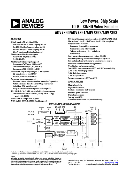
Patented content-dependent low power DAC operation Automatic cable detection and DAC power-down Individual DAC on/off control Sleep mode with minimal power consumption 74.25 MHz 8-/10-/16-bit high definition input support Compliant with SMPTE 274M (1080i), 296M (720p),
PROGRAMMABLE ED/HD FILTERS
SHARPNESS
YCbCr TO
RGB MATRIX
4× FILTER
POWER MANAGEMENT
CONTROL
VIDEO TIMING GENERATOR
16x/4x OVERSAMPLING PLL
Multiformat video input support 4:2:2 YCrCb (SD, ED, and HD) 4:4:4 RGB (SD)
Multiformat video output support Composite (CVBS) and S-Video (Y/C) Component YPrPb (SD, ED, and HD) Component RGB (SD, ED, and HD)
Rev. 0
Information furnished by Analog Devices is believed to be accurate and reliable. However, no responsibility is assumed by Analog Devices for its use, nor for any infringements of patents or other rights of third parties that may result from its use. Specifications subject to change without notice. No license is granted by implication or otherwise under any patent or patent rights of Analog Devices. Trademarks and registered trademarks are the property of their respective owners.
SD Host Controller 2.0设计说明书
SD Host Controller 2.0设计说明书(仅供内部使用)拟制: 张 杰 日期: 2008-8-13审核: 日期:审核: 日期;批准: 日期;创辉电脑深圳代表处香港创辉电脑有限公司深圳代表处研究管理部文档中心 产品版本 密级 V1.0绝密 产品名称: SD Host Controller 2.0修订记录日期修订版本描述作者2008-8-13 1.0 初稿完成张杰目录目录 .................................................................................................................................................. 3第1章总体设计. (5)§1.1 SD卡控制器综述 (5)§1.2 SD卡控制器应用结构图 (5)§1.3 顶层结构图 (6)§1.4 SD卡控制器主要功能点 (6)§1.5 SD卡控制器接口描述 (7)§1.6 SD卡控制器寄存器定义 (8)第2章模块设计与验证 (29)§2.1 命令控制模块(CCL)设计与验证 (29)§2.1.1 模块说明 (29)§2.1.2 模块接口描述 (30)§2.1.3 状态机设计 (32)§2.1.4 功能仿真 (43)§2.2 中断控制/时钟管理模块(Clockgen/INT)设计与验证 (44)§2.2.1 模块说明 (44)§2.2.2 模块接口描述 (44)§2.2.3 模块结构图 (47)§2.2.4 功能仿真 (47)§2.3 数据控制模块(DCL)设计与验证 (50)§2.3.1 模块说明 (50)§2.3.2 详细功能描述 (50)§2.3.3 模块接口描述 (52)§2.3.4 状态机设计 (56)§2.3.5 功能仿真 (56)第3章系统级功能仿真和FPGA验证 (57)§3.1 功能仿真结果表格 (57)§3.2 FPGA验证 (57)第4章LINUX下SD卡驱动程序 (59)§4.1 SDIO驱动程序流程图 (59)§4.2 SD/MMC/SDHC Host 2.0驱动程序流程图 (61)§4.3 相关Card驱动流程图(2.0标准) (67)第5章附录(SD卡控制器验证计划书) (70)§5.1 SD控制器功能验证方案 (70)§5.1.1 验证环境 (70)§5.1.2 验证平台 (70)§5.1.3 验证流程 (71)§5.2 功能点统计 (72)§5.3 详细测试步骤和寄存器设置 (73)§5.4 FPGA验证 (77)§5.4.1 验证目标 (77)§5.4.2 验证方法 (78)§5.4.3 详细验证计划 (78)第6章参与设计人员 (81)第1章总体设计§1.1SD卡控制器综述本设计遵循SD Host Controller Simplified Specification Version2.00版本。
ov7670寄存器配置调试总结
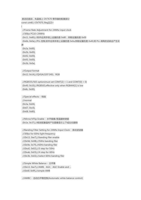
废话后面说,先直接上OV7670寄存器的配置部分const uint8_t OV7670_Reg[][2]={//Frame Rate Adjustment for 24Mhz input clock//30fps PCLK=24MHz{0x11, 0x80},//软件应用手册上设置的是0x80,例程设置的是0x00{0x6b, 0x0a},//PLL控制,软件应用手册上设置的是0x0a,例程设置的是0x40,将PLL调高的话就会产生花屏{0x2a, 0x00},{0x2b, 0x00},{0x92, 0x00},{0x93, 0x00},{0x3b, 0x0a},//Output format{0x12, 0x14},//QVGA(320*240)、RGB//RGB555/565 option(must set COM7[2] = 1 and COM7[0] = 0){0x40, 0x10},//RGB565,effective only when RGB444[1] is low{0x8c, 0x00},//Special effects - 特效//normal{0x3a, 0x04},{0x67, 0xc0},{0x68, 0x80},//Mirror/VFlip Enable - 水平镜像/竖直翻转使能{0x1e, 0x37},//修改配置值将产生图像显示上下或左右颠倒//Banding Filter Setting for 24Mhz Input Clock - 条纹滤波器//30fps for 60Hz light frequency//{0x13, 0xe7},//banding filer enable//{0x9d, 0x98},//50Hz banding filer//{0x9e, 0x7f},//60Hz banding filer//{0xa5, 0x02},//3 step for 50Hz//{0xab, 0x03},//4 step for 60Hz//{0x3b, 0x02},//select 60Hz banding filer//Simple White Balance - 白平衡//{0x13, 0xe7},//AWB、AGC、AGC Enable and ...//{0x6f, 0x9f},//simple AWB//AWBC - 自动白平衡控制(Automatic white balance control)//{0x43, 0x14},//用户手册里这些寄存器的值都是保留(Reserved),不用设置的呀?//{0x44, 0xf0},//{0x45, 0x34},//{0x46, 0x58},//{0x47, 0x28},//{0x48, 0x3a},//AWB Control//{0x59, 0x88},//用户手册连寄存器都是保留,初始值都没提供//{0x5a, 0x88},//{0x5b, 0x44},//{0x5c, 0x67},//{0x5d, 0x49},//{0x5e, 0x0e},//AWB Control//{0x6c, 0x0a},//{0x6d, 0x55},//{0x6e, 0x11},//{0x6f, 0x9f},//AGC/AEC - Automatic Gain Control自动增益补偿/Automatic exposure Control自动曝光控制//{0x00, 0x00},//{0x14, 0x20},//{0x24, 0x75},//{0x25, 0x63},//{0x26, 0xA5},//AEC algorithm selection - AEC公式选择//{0xaa, 0x94},//基于平均值的AEC算法Average-based AEC algorithm/基于直方图的AEC算法Histogram-based AEC algorithm//基于直方图的AGC/AEC的控制//{0x9f, 0x78},//{0xa0, 0x68},//{0xa6, 0xdf},//{0xa7, 0xdf},//{0xa8, 0xf0},//{0xa9, 0x90},//Fix Gain Control - 固定增益控制//{0x69, 0x5d},//Fix gain for Gr channel/for Gb channel/for R channel/for B channel//Color saturation 颜色饱和度+ 0//{0x4f, 0x80},//{0x50, 0x80},//{0x51, 0x00},//{0x52, 0x22},//{0x53, 0x5e},//{0x54, 0x80},//{0x58, 0x9e},//Brightness - 亮度+ 0//{0x55, 0x00},//Contrast - 对比度+ 0//{0x56, 0x40},//Gamma Curve - 伽马曲线//{0x7a, 0x20},//{0x7b, 0x1c},//{0x7c, 0x28},//{0x7d, 0x3c},//{0x7e, 0x55},//{0x7f, 0x68},//{0x80, 0x76},//{0x81, 0x80},//{0x82, 0x88},//{0x83, 0x8f},//{0x84, 0x96},//{0x85, 0xa3},//{0x86, 0xaf},//{0x87, 0xc4},//{0x88, 0xd7},//{0x89, 0xe8},//Matrix Coefficient - 色彩矩阵系数//{0x4f, 0x80},//{0x50, 0x80},//{0x51, 0x00},//{0x52, 0x22},//{0x53, 0x5e},//{0x54, 0x80},//Lens Correction Option - 镜头补偿选项 //{0x62, 0x00},//{0x63, 0x00},//{0x64, 0x04},//{0x65, 0x20},//{0x66, 0x05},//{0x94, 0x04},//effective only when LCC5[2] is high//{0x95, 0x08},//effective only when LCC5[2] is high//注释这些配置的话,就倾斜显示,并显示多块,这到底是控制什么的?跟时序图有关?{0x17, 0x16},//行频Horizontal Frame开始高八位(低三位在HREF[2:0]){0x18, 0x04},//行频Horizontal Frame结束高八位(低三位在HREF[5:3]){0x19, 0x02},//场频Vertical Frame开始高八位(低二位在VREF[1:0]){0x1a, 0x7b},//场频Vertical Frame结束高八位(低二位在VREF[3:2]){0x32, 0x80},//HREF{0x03, 0x06},//VREF//注释这个配置的话,就显示花屏了{0x15, 0x02},//配置PCLK、HREF、VSYNC相关//Automatic black Level Compensation - 自动黑电平校正{0xb0, 0x84},//调试时注释这项配置时,颜色显示不正常了,红色练绿色,绿色变红色,但用户手册对这寄存器是保留RSVD//{0xb1, 0x0c},//{0xb2, 0x0e},//{0xb3, 0x82},//{0xb8, 0x0a},//SCALING_xx寄存器//{0x70, 0x00},//{0x71, 0x00},//{0x72, 0x11},//{0x73, 0x08},//{0x3e, 0x00},//ADC//{0x37, 0x1d},//ADC控制ADC Control//{0x38, 0x71},//ADC和模拟共模控制ADC and Analog Common Mode Control//{0x39, 0x2a},//ADC偏移控制ADC Offset Control//零杂的寄存器//{0x92, 0x00},//空行低八位Dummy Line low 8 bits//{0xa2, 0x02},//像素时钟延时//{0x0c, 0x0c},//{0x10, 0x00},//{0x0d, 0x01},//{0x0f, 0x4b},//{0x3c, 0x78},//{0x74, 0x19},//用户手册里这几个寄存器都是保留RSVD//{0x0e, 0x61},//{0x16, 0x02},//{0x21, 0x02},//{0x22, 0x91},//{0x29, 0x07},//{0x33, 0x0b},//{0x35, 0x0b},//{0x4d, 0x40},//{0x4e, 0x20},//{0x8d, 0x4f},//{0x8e, 0x00},//{0x8f, 0x00},//{0x90, 0x00},//{0x91, 0x00},//{0x96, 0x00},//{0x9a, 0x80},};刚开始学OV7670摄像头,我想大家跟我一样心里很毛躁吧,一个模块需要你配置100多个寄存器,但用户手册对寄存器的介绍却草草的一笔带过,自己无从下手啊,只能看开发板给的例程和上网找一些大虾的帖子了。
3步设置模式(滞后模式)指南说明书
3 Step Setting Mode[3 step setting mode (hysteresis mode)]In the 3 step setting mode, the set value (P_1 or n_1) and hysteresis (H_1) can be changed. After selecting the channel, set the items on the sub display (set value or hysteresis) with the UP or DOWN button. When changing the set value, follow the(1) Press the SET button once when the item tobe changed is displayed on the sub display.The set value on the sub display (right) willstart flashing.button.When UP and DOWN buttons are pressed and held simultaneously for 1 second or longer, the set value is displayed as [- - -], and the set value will be the same as the current pressure value automatically (snap shot function).Afterwards, it is possible to adjust the value by pressing the UP or DOWN button.(3) Press the SET button to complete the setting.The pressure switch turns on within a set pressure range (from P1L to P1H) during window comparator mode.Set P1L, the lower limit of the switch operation, and P1H, the upper limit of the switch operation and WH1 (hysteresis) following the instructions given above.(When reversed output is selected, the sub display (left) shows [n1L] and [n1H].)∗:Set OUT2 in the same way. (ex. P_2, H_2)∗:Setting of the normal/reverse output switching and hysteresis/window comparator mode switching are performed with the function selection mode [F 1] OUT1 setting and [F 2]OUT2 setting.value Simple Setting Mode(1) After selecting the channel, press the SET button for 1 second or longer, but less than 3 seconds, in measurement mode. [SEt] is displayed on the main display. When the button is released while in the [SEt] display, the current pressure value is displayed on the main display, [P_1] or [n_1] is displayed on the sub display (left),and the set value is displayed on the sub display (right) (Flashing).(2) Change the set value with UP or DOWN button, and press the SET button to set the value. Then, the setting moves to hysteresis setting.(The snap shot function can be used.)(3) Change the set value with UP or DOWN button, and press the SET button to set the value. Then, the setting moves to the delay time of the switch output.(The snap shot function can be used.)(4) Press the UP or DOWN button, the delay time of the switch output can be selected.Delay time setting can prevent the output from chattering.(5) Press the SET button for 2 seconds or longer to complete the setting.∗:If the button is pressed for less than 2 seconds , the setting will moves to the OUT2 setting.In the window comparator mode, set P1L, the lower limit of the switch operation,and P1H, the upper limit of the switch operation, WH1 (hysteresis) and dt1 (delay time) following the instructions given above.(When reversed output is selected, the sub display (left) shows [n1L] and [n1H].)∗:Set OUT2 in the same way.Default settingThe default setting is as follows.If no problem is caused by this setting, keep these settings.[F 0] Differential pressure check mode,(URL ) for more detailed information, or contact SMC.[F 1] Setting of OUT1Same setting as [F 1] OUT1.Other SettingsChannel scan function•Press the UP button for 2 seconds or longer. Channels and the measured pressures will be displayed in order approximately every 2 seconds.•The function can be released by pressing the UP button again for 2 seconds or longer .∗:Channel scan function will remain even when the power supply is turned off.∗:During channel scan, setting is disabled other than channel scan mode release and key lock function setting.Release the channel scan mode when changing settings.Snap shot functionThe current pressure value can be stored to the switch output ON/OFF set point.Peak/bottom value indicationThe max. (min.) pressure when the power is supplied is detected and updated.The value can be displayed on the sub display by pressing DOWN button in measurement mode.Zero-clear functionIn measurement mode, when the UP and DOWN buttons are pressed for 1second or longer simultaneously, the main display shows [- - -], and the reset to zero. The display returns to measurement mode automatically.Key-lock functionTo set each of these functions, refer to the SMC website(URL ) for more detailed information, or contact SMC.MaintenanceHow to reset the product after a power cut or forcible de-energizingThe setting of the product will be retained as it was before a power cut or de-energizing.The output condition is also basically recovered to that before a power cut or de-energizing, but may change depending on the operating environment. Therefore, check the safety of the whole installation before operating the product. If the installation is using accurate control, wait until the product has warmed up (approximately 10 to 15 minutes).Note: Specifications are subject to change without prior notice and any obligation on the part of the manufacturer.© 2018 SMC Corporation All Rights Reserved Specifications/Outline with Dimensions (in mm)Refer to the product catalogue or SMC website (URL ) for more information about the product specifications and outline dimensions.TroubleshootingError indication functionthan above are displayed, please contact SMC.Refer to the SMC website (URL ) for more information about troubleshooting.PS ※※-OMW0006Akihabara UDX 15F, 4-14-1, Sotokanda, Chiyoda-ku, Tokyo 101-0021, JAPAN Phone: +81 3-5207-8249 Fax: +81 3-5298-5362URL Before UseMulti-channel Digital Sensor MonitorPSE20#A SeriesSummary of Product partsPress the SET button once.and 5 sec.∗: If a button operation is not performed for 3 seconds during the setting, the display will flash.(This is to prevent the setting from remaining incomplete if, for instance, an operator were to leave during setting.)∗: 3 step setting mode, simple setting mode and function selection mode settings are reflected each other.SET button between 1and 3 sec.Thank you for purchasing an SMC PSE20#A Series Multi-channel Digital Sensor Monitor.Please read this manual carefully before operating the product and make sure you understand its capabilities and limitations. Please keep this manual handy for future reference.Safety InstructionsThese safety instructions are intended to prevent hazardous situations and/or equipment damage.These instructions indicate the level of potential hazard with the labels of"Caution", "Warning" or "Danger". They are all important notes for safety and must be followed in addition to International standards (ISO/IEC) and other safety regulations.OperatorSafety InstructionsInstallationMounting by panel mount adapterFix the panel mount adapter to the Controller with the set screws M3 x 8L (2 pcs.) as attached.•Panel mount adapter (Model: ZS-26-B)Panel mount adapter + Front protective cover (Model: ZS-26-01)□48 conversion adapter (Model: ZS-26-D)∗: The panel mount adapter can be rotated by 90 degrees for mounting.∗: Front panel of this Controller meets IP65 (if □48 conversion adapter is used, it meets IP40).However, if the panel mount adapter is hold enough with screw and the instrument is not seated correctly, water might enter. Screw shall be tightened 1/4 to 1/2 turns more after touched correctly.(Model: ZS-26-01)Refer to the product catalogue or SMC website (URL )for more information about panel cut-out and mounting hole dimensions.WiringWiring connectionsConnections should be made with the power supply turned off.Use a separate route for the product wiring and any power or high voltage wiring. Otherwise, malfunction may result due to noise.If a commercially available switching power supply is used, be sure to ground the frame ground (FG) terminal. If the switching power supply is connected for use, switching noise will be superimposed and it will not be able to meet the product specifications. In that case, insert a noise filter such as a line noise filter/ferrite between the switching power supplies or change the switching power supply to the series power supply.Attaching the connector to the lead wireSensor wire is stripped as shown in the right figure.(Refer to the table below for correspondence between connectorand electrical wire gauge.)The core of the corresponding colour shown in the following table is put into the pin of the number stamped on the connector for sensor connection to the back.correctly, and part A shown in the figure is pushed by hand and makes temporary connection.Part A centre is pushed straight in using a suitable tool, such as pliers.Re-use cannot be performed once it connects the connector for sensor connection completely. When the connection fails or a pin is miswired,please use a new connector for sensor connection.When the sensor is not connected correctly, [LLL] will be displayed.Cable wire colour is applicable when an SMC sensor with lead wire is used.ConnectorConnecting/DisconnectingWhen connecting the connector,insert it straight onto the pin and lock the connector into the square groove in the housing until connector clicks.When removing the connector, press down the lever with your thumb and pull the connector straight out.Pin No. of the connectorPin No.CH4_OUT1Auto shift input CH3_OUT1CH2_OUT1CH1_OUT2CH1_OUT1DC(-)DC(+)DOWN button once.Function selection modeAfter selecting the channel, inmeasurement mode, press the SET button for 3 seconds or longer (but less than 5 seconds), to display [F 0]. Select to display the function to be changed [F ]. Press and hold the SET button for 2 seconds or longer in function selection mode to return to measurement mode.∗:to configuration of other functions, [- - -] is displayed on the sub display (right).∗:All channel indicators turn on for the setting which is common for all channels.。
NI ELVIS II系列产品规格说明说明书
Arbitrary Waveform Generator/Analog Output
Number of channels.........................2
DAC resolution................................16 bits
DNL.................................................±1 LSB
Maximum working voltage for analog inputs (signal + common mode) ................ ±11 V of AIGND
CMRR (DC to 60 Hz) ..................... 90 dB
Source..............................................AI<0..15>, ScopeCH0, ScopeCH1
Small signal bandwidth (–3 dB)......1.2 MHz
Input FIFO size................................4095 samples
Scanlist memory ..............................4095 entries
Data B signal stream, programmed I/O
timing-distxref
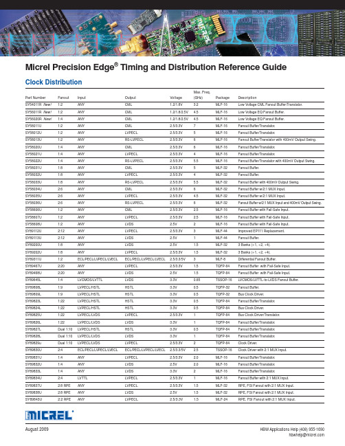
Micrel Precision Edge® Timing and Distribution Reference GuideClock DistributionMax. Freq.Part Number Fanout Input Output Voltage (GHz) Package DescriptionSY54011R New!1:2 ANY CML 1.2/1.8V 3.2 MLF-16 Low Voltage CML Fanout Buffer/Translator.SY56011R New!1:2 ANY CML 1.2/1.8/2.5V 4.5 MLF-16 Low Voltage EQ Fanout Buffer.SY56020R New!1:4 ANY CML 1.2/1.8/2.5V 4.5 MLF-16 Low Voltage EQ Fanout Buffer.Buffer/Translator.Fanout7 MLF-16SY58011U 1:2 ANY CML 2.5/3.3VFanoutBuffer/Translator.5 MLF-16SY58012U 1:2 ANY LVPECL 2.5/3.3VBuffer/Translator with 400mV Output Swing.6 MLF-16 FanoutSY58013U 1:2 ANY RS-LVPECL 2.5/3.3VBuffer/Translator.FanoutSY58020U 1:4 ANY CML 2.5/3.3V6 MLF-16Buffer/Translator.Fanout4 MLF-16SY58021U 1:4 ANY LVPECL 2.5/3.3VSY58022U 1:4 ANY RS-LVPECL 2.5/3.3V 5.5 MLF-16 Fanout Buffer/Translator with 400mV Output Swing.Buffer.Fanout5 MLF-32SY58031U 1:8 ANY CML 2.5/3.3VBuffer.FanoutSY58032U 1:8 ANY LVPECL 2.5/3.3V4 MLF-32SY58033U 1:8 ANY RS-LVPECL 2.5/3.3V 5.5 MLF-32 Fanout Buffer with 400mV Output Swing.SY58034U 2:6 ANY CML 2.5/3.3V 6 MLF-32 Fanout Buffer w/2:1 MUX Input.SY58035U 2:6 ANY LVPECL 2.5/3.3V 4.5 MLF-32 Fanout Buffer w/2:1 MUX Input.6 MLF-32Fanout Buffer w/2:1 MUX Input and 400mV Output Swing. SY58036U 2:6 ANY RS-LVPECL 2.5/3.3VSY58606U 1:2 ANY CML 2.5/3.3V 2.5 MLF-16 Fanout Buffer with Fail-Safe Input.SY58607U 1:2 ANY LVPECL 2.5/3.3V 2.5 MLF-16 Fanout Buffer with Fail-Safe Input.SY58608U 1:2 ANY LVDS 2.5V 2 MLF-16 Fanout Buffer with Fail-Safe Input.SY89112U 2:12 ANY LVPECL 2.5/3.3V 3 MLF-44 Improved EP111 Replacement.SY89113U 2:12 ANY LVDS 2.5V 1 MLF-44Buffer.FanoutSY89200U 1:8 ANY LVDS 2.5V 1.5 MLF-32 3 Banks (÷1, ÷2, ÷4).SY89202U 1:8 ANY LVPECL 2.5/3.3V 1.5 MLF-32 3 Banks (÷1, ÷2, ÷4).SY89311U 1:2 ECL/PECL/LVPECL/LVECL ECL/PECL/LVPECL/LVECL 2.5/3.3/5V 3 MLF-8 Differential Fanout Buffer.SY89467U2:20 ANY LVPECL 2.5/3.3V 1.5 TQFP-64 Fanout Buffer with Fail-Safe Input.SY89468U2:20 ANY LVDS 2.5V 1.5 TQFP-64 Fanout Buffer with Fail-Safe Input.SY89645L 1:4 LVCMOS/LVTTL LVDS 3.3V 0.65 TSSOP-16 LVCMOS/LVTTL-to-LVDS Fanout Buffer.Buffer.FanoutSY89808L 1:9 LVPECL/HSTL HSTL 3.3V 0.5 TQFP-32SY89809L 1:9 LVPECL/HSTL HSTL 3.3V 0.5 TQFP-32 Bus Clock Driver.Buffer/Translator.SY89823L 1:22 LVPECL/HSTL HSTL 3.3V 0.5 TQFP-64FanoutSY89824L 1:22 LVPECL/HSTL HSTL 3.3V 0.5 TQFP-64 Bus Clock Driver.SY89825U 1:22 LVPECL/LVDS LVPECL 2.5/3.3V 1 TQFP-64 Bus Clock Driver/Translator.Buffer/Translator.SY89826L 1:22 LVPECL/LVDS LVDS 3.3V 1 TQFP-64FanoutSY89827L Dual 1:10 LVPECL/HSTL HSTL 3.3V 0.5 TQFP-64 Fanout Buffer/Translator.SY89828L Dual 1:10 LVPECL/LVDS LVDS 3.3V 1 TQFP-64 Fanout Buffer/Translator.SY89829u Dual 1:10 LVPECL/LVDS LVPECL 2.5/3.3V 2 TQFP-64 Clock Driver.SY89830U 2:4 ECL/PECL/LVPECL/LVECL ECL/PECL/LVPECL/LVECL 2.5/3.3/5V 2.5 TSSOP-16 Clock Driver with 2:1 MUX Input.Buffer/Translator.Fanout2.0 MLF-16SY89831U 1:4 ANY LVPECL 2.5/3.3VBuffer/Translator.SY89832U 1:4 ANY LVDS 2.5V 2.0 MLF-16FanoutBuffer/Translator.SY89833L 1:4 ANY LVDS 3.3V 2 MLF-16FanoutSY89834U 2:4 LVTTL LVPECL 2.5/3.3V 1 MLF-16 Fanout Buffer with 2:1 MUX Input.SY89837U 2:8 RPE ANY LVPECL 2.5/3.3V 1.5 MLF-32 RPE, FSI Fanout with 2:1 MUX Input.SY89838U 2:8 RPE ANY LVDS 2.5V 1.5 MLF-32 RPE, FSI Fanout with 2:1 MUX Input.SY89843U 2:2 RPE ANY LVPECL 2.5/3.3V 1.5 MLF-24 RPE, FSI Fanout with 2:1 MUX Input.Clock Dividers/GeneratorsFanout Max. Freq.Part Number Buffer Input Output Voltage (GHz) Package DescriptionSY89200U Y ANY LVDS 2.5V 1.5 MLF-32 3 Banks (÷1, ÷2, ÷4) 8 Total.SY89202U Y ANY LVPECL 2.5/3.3V 1.5 MLF-32 3 Banks (÷1, ÷2, ÷4) 8 Total.SY89218U Y ANY LVDS 2.5V 1.5 TQFP-64 4 Banks (÷1, ÷2, ÷4) 15 Total FSI Input.SY89221U Y ANY LVPECL 2.5/3.3V 1.5 TQFP-64 4 Banks (÷1, ÷2, ÷4) 15 Total FSI Input.SY89228U N ANY LVPECL 2.5/3.3V 1 MLF-16 ÷3, ÷5 FSI Input.SY89229U NANYLVDS2.5V1MLF-16÷3, ÷5 FSI Input.SY89230U N ANY LVPECL 2.5/3.3V 3.2 MLF-16 ÷3, ÷5.SY89231UN ANYLVDS2.5V3.2 MLF-16 ÷3, ÷5.SY89312V N ECL/PECL ECL/PECL 3.3/5V 4 MLF-8 ÷2.SY89313V N ECL/PECL ECL/PECL 3.3/5V 4 MLF-8 ÷4.SY89871U Y ANY LVPECL 2.5/3.3V 2.5 MLF-16 2 Banks (÷1, ÷2, ÷4, ÷8, ÷16).SY89872U Y ANY LVDS 2.5V 2 MLF-16 2 Banks (÷1, ÷2, ÷4, ÷8, ÷16).SY89873L Y ANY LVDS 3.3V 2 MLF-16 2 Banks (÷1, ÷2, ÷4, ÷8, ÷16).SY89874U Y ANY LVPECL 2.5/3.3V 2.5 MLF-16 ÷1, ÷2, ÷4, ÷8, ÷16.SY89875U Y ANY LVDS 2.5V 2 MLF-16 ÷1, ÷2, ÷4, ÷8, ÷16.SY89876L Y ANYLVDS 3.3V 2 MLF-16 ÷1, ÷2, ÷4, ÷8, ÷16.SY100S834L N ECL/PECL/LVPECL ECL/PECL 3.3/5V — SOIC-16 (÷1, 2, 4) or (÷2, 4, 8).SY100S838L N ECL/PECL/LVPECL ECL/PECL 3.3/5V — SOIC-20 (÷1, 2/3) or (÷2, 4/6).SY100S839V N ECL/PECL/LVPECL ECL/PECL 3.3/5V — SOIC-20 (÷2/4) or (÷4/5/6).SY10/100EL32V N ECL ECL 3.3/5V 3 SOIC-8 ÷2. SY10/100EL33/L N ECL ECL 3.3/5V 4 SOIC-8 ÷4.SY10/100EL34/L Y ECL ECL 3.3/5V — SOIC-16 3 Outputs ÷2, 4, or 8. SY10/100EL38/LYECLECL3.3/5V—SOIC-202 Banks (÷2) ,(÷4/6).Clock Distribution (continued)Max. Freq. Part Number Fanout Input Output Voltage (GHz) Package DescriptionSY89844U 2:2 RPE ANY LVDS 2.5V 1.5 MLF-24 RPE, FSI Fanout with 2:1 MUX Input.SY89464U 2:10 RPE ANY LVPECL 2.5/3.3V 2 MLF-44 RPE, FSI Input MUX with 2:1 MUX Input.SY89465U 2:10 RPE ANY LVDS 2.5V 2 MLF-44 RPE, FSI Input MUX with 2:1 MUX Input.SY89473U 2:2 ANY LVPECL 2.5/3.3V 3 MLF-24 Fanout Buffer/Translator.SY89474U 2:2 ANY LVDS 2.5V 2.5 MLF-24 Fanout Buffer/Translator.SY89846U 2:5 ANY LVPECL 2.5/3.3V 1.5 MLF-32 Fanout Buffer with Fail-Safe Input.SY89847U 2:5 ANY LVDS 2.5V 1.5 MLF-32 Fanout Buffer with Fail-Safe Input.SY89850U 1:1 ANY LVPECL 2.5/3.3V 4 MLF-8 LVPECL Line Driver/Receiver.SY89851U 1:2 ANY LVPECL 2.5/3.3V 3 MLF-16 Low Power Fanout Buffer/Trans.SY89854U 1:4 ANY LVPECL 2.5/3.3V 3.5 MLF-16 Low Power Fanout Buffer/Trans.SY89856U 2:6 ANY LVPECL 2.5/3.3V 3 MLF-32 Low Power Fanout Buffer with 2:1 MUX Input.SY89858U1:8ANYLVPECL2.5/3.3V3MLF-32Low Power Fanout Buffer.SY897132L New! 1:2 LVPECL LVPECL 3.3V 0.8 TSSOP-28 Link Replicator.SY898533L New! 1:4 LVPECL LVPECL 3.3V 0.7 TSSOP-20 Fanout Buffer.SY10/100E111 1:9 PECL PECL 5V 0.75 PLCC-28 With Enable.SY10/100E111A/L 1:9 PECL PECL 3.3/5V 0.75 PLCC-28 SY10/100E111AE/LE 1:9 PECL PECL 3.3/5V 0.75 PLCC-28 With Enable. SY10/100EL11V 1:2 PECL PECL 3.3/5V 0.75 SOIC-8 SY10/100EL15 1:4 PECL PECL 5V 0.75 SOIC-16 With Enable.SY100EL14V 1:5 PECL PECL 3.3/5V 0.75 SOIC-20 With Enable. SY100EL15L 1:4 PECL PECL 3.3V 0.75 SOIC-16 With Enable. SY100HA643 1:8 ECL TTL 5/-5V 0.75 PLCC-28 With Enable. SY100S811 1:9 PECL/TTL PECL 5V 0.75 PLCC/SOIC-28 With Enable. SY100S8151:4PECL/TTLPECL5V0.75SOIC-16With Enable.MaxFreq.MinFreq.Number Input Output Voltage (MHz) (MHz) Package DescriptionPartTQFP-32 AnyClock® Fractional-N Synthesizer.SY87729L XTAL PECL 3.3V 10 365SY87739L XTAL PECL 3.3V 10 730TQFP-32 AnyClock® Fractional-N Synthesizer.SY89426 TTL PECL 5V 33 622 PLCC-28 SONET OC-12/OC -3.SY89529L XTAL LVPECL 3.3V — 200 TQFP-32, SOIC-28 Spectrum Clock Synthesizer.SY89531L XTAL HSTL/LVPECL 3.3V 33 500 TQFP-64 XTAL Input Synthersizer.SY89532L XTAL LVPECL 3.3V 33 500 TQFP-64 XTAL Input Synthesizer.SY89533L XTAL LVDS/LVPECL 3.3V 33 500 TQFP-64 XTAL Input Synthesizer.SY89534L ANYX LVPECL 3.3V 33 500 TQFP-64 Reference Input Synthesizer.SY89535L ANYX LVDS/LVPECL 3.3V 33 500 TQFP-64 Reference Input Synthesizer.SY89536L ANYX HSTL/LVPECL 3.3V 33 500 TQFP-64 Reference Input Synthesizer.SY89537L ANYX LVDS/LVPECL 3.3V 73 750 MLF-44 Reference and XTAL Prog. Frequency.SY89538L ANYX LVDS/LVPECL 3.3V 73 750 TQFP-64 Reference Input, Multiple Banks, Zero Delay. SY89610L ANY CML 3.3V 19 694 MLF-32 Clock Synthesizer with Ultra Low Jitter. Receivers/Buffers/DriversMax. Data Max. Freq.Part Number Input Output Voltage Rate (Gbps) (GHz) Package DescriptionSY54016R New!ANY CML 1.2/1.8V 3.2 2.5 MLF-8 (2 x 2mm) Low Voltage CML Translator with Fail-Safe Input. SY54016AR New!ANY CML 1.2/1.8V 3.2 3.2 MLF-8 (2 x 2mm) Low Voltage CML Translator.SY56016R New!ANY CML 1.2/1.8/2.5V 6.4 5 MLF-10 (2 x 2mm) Differential Line Driver with EQ.SY56216R New!ANY CML 1.2/1.8/2.5V 6.4 5 MLF-16 (3 x 3mm) Dual Channel EQ Receiver.SY58016L CML/PECL CML 3.3V 10.7 7 MLF-16 (3 x 3mm) Differential CML Line Driver/Receiver.SY58600U ANY CML 2.5/3.3V 10.7 7 MLF-8 (2 x 2mm) Line Driver/Receiver.SY58601U ANY LVPECL 2.5/3.3V 5 5 MLF-8 (2 x 2mm) Line Driver/Receiver.SY58602U ANY RS-LVPECL 2.5/3.3V 10.7 7 MLF-8 (2 x 2mm) Line Driver with 400mV Output Swing.SY58603U ANY CML 2.5/3.3V 4.25 2.5 MLF-8 (2 x 2mm) Line/Driver Receiver with Fail-Safe Input.SY58604U ANY LVPECL 2.5/3.3V 3.2 2.5 MLF-8 (2 x 2mm) Line/Driver Receiver with Fail-Safe Input.SY58605U ANY LVDS 2.5V 3.2 2 MLF-8 (2 x 2mm) Line/Driver Receiver with Fail-Safe Input.SY58620L ANY CML 3.3V 4.25 2.5 MLF-24 (4 x 4mm) Backplane Transceiver.SY89206V ECL/PECL ECL/PECL 3.3/5V — 1 MLF-8 (2 x 2mm) Receiver/Buffer-100k Comp.SY89207L LVECL/LVPECL PECL 3.3V — 0.8 MSOP-10 Amp. w/Low-Gain Feedback.SY89216V ECL/PECL ECL/PECL 3.3/5V — 1 MLF-8 (2 x 2mm) Receiver/Buffer-10k Comp.SY89250V ECL/PECL ECL/PECL 3.3/5V — — MLF-8 (2 x 2mm) Enhanced Differential Receiver.SY89306V ECL/PECL ECL/PECL 3.3/5V — 2.5 MLF-8 (2 x 2mm) Receiver/Buffer-100k Comp.SY89307V ECL/PECL ECL/PECL 3.3/5V 2.5 — MLF-8 (2 x 2mm) Variable Output Swing Differential Receiver.SY89316V ECL/PECL ECL/PECL 3.3/5V — 2.5 MLF-8 (2 x 2mm) Differential Receiver/Buffer-10k Comp.SY89835U LVDS LVDS 2.5V 3.2 2 MLF-8 (2 x 2mm) Buffer with Fail-Safe Input.SY89850U CML/PECL/LVDS LVPECL 2.5/3.3V 3.2 4 MLF-8 (2 x 2mm) Low Power.Driver.SY10/100E112 ECL/PECLECL/PECL 5V — — PLCC-28 QuadSY10/100E116 ECL/PECL ECL/PECL 5V — — PLCC-28 Quint Differential Line Driver.SY10/100E416 ECL/PECL ECL/PECL 5V — — PLCC-28 Quint Differential Line Driver.Driver.Impedance ECL/PECLECL/PECL 5V — — SOIC-8 LowSY10/100EL12Receiver.SY10/100EL16V ECL/LVPECLECL/LVPECL 3.3/5V — — SOIC/MSOP-8 DifferentialSY10/100EL16VA-VF ECL/LVPECL ECL/LVPECL 3.3/5V — — SOIC/MSOP-8 Enhanced Differential Receiver.SY10/100EL16VS ECL/LVPECL ECL/LVPECL 3.3/5V — — SOIC/MSOP-8 Variable Output Swing Receiver.Receiver.DifferentialECL/LVPECLSY100EL17V ECL/LVPECL3.3/5V — — SOIC-20 QuadSY10EL1189 ECL/PECL ECL/PECL 5V — — SOIC-16 FC Coaxial Cable Driver.SY10EL89 ECL/LVPECLECL/LVPECLDriver.Cable3.3/5V — — SOIC-8 CoaxialSY10/100EP16U ECL/PECL ECL/PECL 2.5/3.3V 2.5 4 MLF-8 (2 x 2mm) ECL Differential Receiver/Driver.SY100EP16V ECL/PECL ECL/PECL 3.3/5V 2.5 4 MLF-8 (2 x 2mm) ECL Differential Receiver/Driver.Skew ManagementFreq.Max.Part Number Input Output Voltage (GHz) Package ChannelsSY89295U LVPECL/LVTTL LVPECL 2.5/3.3V 1.5 TQFP/MLF-32 Programmable Delay.SY89296U LVPECL/LVTTL LVPECL 2.5/3.3V 1.5 TQFP/MLF-32 Programmable Delay with Fine Tune Control. SY89297U New!ANY CML 2.5V 1.6/3.2(Gbps) MLF-24 5ps /Step Programmable Delay, Dual Channel. SY55856U CML CML 2.5/3.3V 2.5 TQFP-32 Two Channel Delay Line. Crosspoint SwitchesMax. Data RatePart Number Input Output Voltage (Gbps) Package DescriptionSY54023R New!ANY CML 1.2/1.8V 3.2 MLF-16 2x2 with Fail-Safe Inputs.SY56023R New!ANY CML 1.2/1.8/2.5V 6.4 MLF-16 2x2 with Equalization.SY56034AR New!ANY CML 1.2/1.8/2.5V 6.4 MLF-32 2x2 Crosspoint Switch with Six Outputs.SY56040AR New!ANY CML 1.2/1.8/2.5V 6.4 MLF-44 4x4 Crosspoint Switch.SY58023U ANY CML 2.5/3.3V 10.7 MLF-16 2x2.2x2.SY58024U ANY CML 2.5/3.3V 10.7 MLF-32 DualSY58040U ANY CML 2.5/3.3V 5 MLF-44 4x4.SY89540U ANY LVDS 2.5V 3.2 MLF-44 4x4.SY55854U ANY CML 2.5/3.3/5V 2.5 QSOP-16 2x2.2x2.SY55858U CML/PECL/LVPECLCML 2.5/3.3V 3 TQFP-32 Dual2x2.SY55859L CML CML 3.3V 2.7 MLF-32 DualRegisters and Flip-FlopsPart Number Channels Voltage Max. Feq. Package DescriptionSY10/100E131 Quad 5V 1.1 PLCC-28 4-Bit D Flip Flop.SY10/100E141 Single 5V 0.7 PLCC-28 8-Bit Shift Register.SY10/100E142 Single 5V 0.7 PLCC-28 9-Bit Shift Register.SY10/100E151 Single 5V 1.1 PLCC-28 6-Bit D Register.SY10/100E451 Single 5V 1.1 PLCC-28 6-Bit D Register.SY10/100E452 Single 5V 1.1 PLCC-28 5-Bit D Register.SY10/100EL31 Single 5V 2.8 PLCC-28 D Flip Flop w/ Set & Reset.SY10/100EL35 Single 5V 2.2 SOIC-8 JK Flip Flop.SY10/100EL51 Single 5V 2.8 SOIC-8 Differential Clock D Flip Flop.SY10/100EL52 Single 5V 2.0 SOIC-8 Differential Data & Clock D Flip Flop.SY100S331 Single 5V 0.8 PLCC-28 Triple D Flip Flop.SY100S351 Single 5V 0.7 PLCC-28 Hex D Flip Flop.SY100S341 Single 5V 0.6 PLCC-28 8-Bit Shift Register.Transceiver.SY10/100S891 Single 5V — PLCC-28 5-BitRegistered。
vivado上下沿处罚源语
vivado上下沿处罚源语
Vivado是一款电路设计软件,在使用中,我们可能会遇到上下沿处罚源语的问题。
那么,什么是上下沿处罚源语呢?
上下沿处罚源语是在使用Vivado时用来解决时序问题的工具。
具体来说,当设计中的信号出现上升沿或下降沿时,可能会导致其他信号的不稳定,从而影响设计的正常工作。
上下沿处罚源语就是用来解决这个问题的,它可以在信号出现上升沿或下降沿时,对不稳定的信号进行处罚,从而确保设计的正常工作。
使用上下沿处罚源语的方法是:在Vivado中打开设计文件,在设计中找到需要处理的信号,右键单击选择“Create Timing Exception”,在弹出的窗口中选择“Create on Edge Timing Exception”,在“Edge Type”中选择“Rising”或“Falling”,然后点击“OK”即可创建上下沿处罚源语。
上下沿处罚源语是Vivado中很实用的工具,使用它可以有效解决设计中的时序问题,确保设计的正常工作。
上海几大外企数字后端PR-APR-面试终极资料!!你懂的!!

后端试题1.老是简单的问题比较无趣,问一个貌似简单,但是不容易回答完整的How to fix x-talk violation?如何解决线间干扰?难度:4 (关于难度的定义,在第一题里面)(应该至少有5大类解决办法,wire spacing, shielding, change layer 之类的只算其中1类)答案:1)upsize victim net driver, downsize aggressor net driver2)increase wire space, shielding, change layer,change wire width 3)insert butter in victim net能答出以上3条的,在工作中已经基本够用,但是还有两个不常用到的,是AMD的一个大牛告诉我的。
4)把与victim net相连的输入端改成Hi-Vth的单元5)改变信号的timing window。
这个不易做到,但是也是解决方法2.What are several factors to improve propagation delay of standard cell?哪些因素可以影响标准单元的延迟?难度:3答案:1)PVT2)input transition,output load3)Vth3.What would you do in order to not use certain cells from the library?如何禁止使用库里面的某些单元?难度:1答案:set_dont_useset_dont_touch4.During the synthesis, what type of wire load model are often used?做RTL综合时,经常使用的wire load model有哪几种?难度:2注意:问题是wire load model,不是wire load mode,也不是delay model1)zero wire load model2)基于fanout的传统WLM3)基于物理位置(距离)的wire load model,在Cadence的RC中叫PLE,Synopsys 叫DC Ultra Topographical附加问题:What types of delay model are used in digital design? (数字IC设计中有多少种类型的delay model)答案:NLDMCCSECSM还有一个现在基本不用了的—LDM5.How delays are characterized using WLM (Wire Load Model)?使用一般的WLM (不是zero WLM,也不是按照物理位置算的DCT),DC是如何计算delay的?难度:2答案:DC在计算延时的时候,net的rc就要根据所选取的wrie load model来计算,计算时和输出的fanout决定以smic13的smic13_wl10为例wire_load("smic13_wl10") {resistance : 8.5e-8;capacitance : 1.5e-4;area : 0.7;slope : 66.667;fanout_length (1,66.667);根据fanout值,由fanout(1,66.667)可以得出互连线长度为66.667,然后根据resistance 和capacitance计算出互连线电容为1.5e-4*66.667,互连线电阻为8.5e-8*66.667,当然如果扇出值表中没有,就会用到slope,例如扇出为3时,此时估算的互连线长度为1*66.667+(3-1)*slope,再计算出RC值,然后DC由此计算net的延时。
- 1、下载文档前请自行甄别文档内容的完整性,平台不提供额外的编辑、内容补充、找答案等附加服务。
- 2、"仅部分预览"的文档,不可在线预览部分如存在完整性等问题,可反馈申请退款(可完整预览的文档不适用该条件!)。
- 3、如文档侵犯您的权益,请联系客服反馈,我们会尽快为您处理(人工客服工作时间:9:00-18:30)。
Ci = Ai Bi + (Ai + Bi )Ci-1 = Gi + Pi Ci-1
18
Carry-Lookahead Addition
• Step 1: Compute Gi and Pi for all columns • Step 2: Compute G and P for k-bit blocks • Step 3: Cin propagates through each k-bit propagate/generate block
Gi:j = Gi + Pi (Gi-1 + Pi-1 (Gi-2 + Pi-2Gj ) Pi:j = PiPi-1 Pi-2Pj Ci = Gi:j + Pi:j Cj-1
20
32-bit CLA with 4-bit Blocks
B31:28 A31:28 Cout B27:24 A27:24 B7:4 A7:4 B3:0 A3:0 Cin 4-bit CLA C27 4-bit CLA C23 Block Block S31:28 S27:24 C7 4-bit CLA C3 4-bit CLA Block Block S7:4 S3:0
•
•
15
Schematic
• Schematic
• Critical path
A31 Cout + S31 B31 A30 + S30 B30 C29 C1 A1 + S1 B1 C0 A0 + S0 B0 Cin
C30
16
Types of Adders
• Ripple-carry (RCA) (slow) • Carry-lookahead (CLA) (fast) • Study for your homework • MUST DO, as you will use it in lab session next week • Carry-lookahead adder faster for large adders but require more hardware
Embedded System Architecture Design
lecture 03 --Timing and Adders
Jun WANG
1
Outline
• Timing
– Critical path – Glitch
• Adder
– HFA – FA – RCA – CLA
2
Timing
S 0 1 1 0
S =AB Cout = AB
Cin 0 0 0 0 1 1 1 1
A 0 0 1 1 0 0 1 1
B 0 1 0 1 0 1 0 1
Cout 0 0 0 1 0 1 1 1
S 0 1 1 0 1 0 0 1
S = A B Cin Cout = AB + ACin + BCin
Critical Path 1 Y=1 0 1
n2
1
0
B n2
n1 Y Time
7
glitch
Fixing the Glitch
Y C 0 1 AC AB 00 1 1 01 0 1 11 0 1 10 0 0
Y = AB + BC + AC
A=0 B=1 0 Y=1 C=1
8
Why Understand Glitches?
12
Ripple-Carry Adder
• Chain 1-bit adders together • Carry ripples through entire chain • Disadvantage: slow
A31 Cout + S31 B31 A30 + S30 B30 C29 C1 A1 + S1 B1 C0 A0 + S0 B0 Cin
• Glitches don’t cause problems because of synchronous design conventions (see Chapter 3) • It’s important to recognize a glitch: in simulations or on oscilloscope • Can’t get rid of all glitches – simultaneous transitions on multiple inputs can also cause glitches
B3 + S3 G3:0
A3 C2
B2 + S2
A2 C1
B1 + S1
A1 C0
B0 + S0
A0 Cin
G3 P3 G2 P2 G1 P1 G0 P3 P2 P1 P0
Cout Cin
P3:0
21
Summary
• Always/Initial @() vs assign
– Procedural assignment vs continuous assignment
• Column i will generate a carry out if Ai AND Bi are both 1.
G i = Ai Bi
• Column i will propagate a carry in to the carry out if Ai OR Bi is 1.
Pi = Ai + Bi
C30
13
Ripple-Carry Adder Delay
tripple = NtFA
where tFA is the delay of a full adder
Is it too LONG?
14
verilog
• 1 bit FA ( with RTL description ) module FA( input a, b, cin output cout, sum ); // HDL modeling of 1 bit // full adder functionality 。。。 // complete them endmodule 4 bit FA ( with structural description ) module adder( input[3:0] A, B, output cout, output[3:0] S ); wirec0, c1, c2; FA fa0(A[0], B[0], 1’b0, c0, S[0] ); FA fa1( ... ); //complete them FA fa2( ... ); FA fa3( ... ); endmodule How is behavioral description?
17
Carry-Lookahead Adder
• Compute carry out (Cout) for k-bit blocks using generate and propagate signals • Some definitions:
– Column i produces a carry out by either generating a carry out or propagating a carry in to the carry out – Generate (Gi) and propagate (Pi) signals for each column:
• wire vs reg
– wire used only in assign, synthesized as combinational circuit (net) – reg used only in always, synthesized as
• combinational circuit (net), in @(a or b) • Sequential circuit (register), in @(clk)
• Delay between input change and output changing • How to build fast circuits?
A Y
delay A Y Time
3
Critical (Long) & Short Paths
Critical Path A B C D Short Path Y n1 n2
• What happens when A = 0, C = 1, B falls?
A B Y C Y C 0 1 AB 00 1 1 01 0 1 11 0 1 10 0 0
Y = AB + BC
6
Glitch Example (cont.)
A=0 B=1 0 C=1 Short Path 0
n1
B 0 1 0 1 0 1 0 1
Cout 0 0 0 1 0 1 1 1
S 0 1 1 0 1 0 0 1
S = Cout =
11
1-Bit Adders
Half Adder
A Cout B Cout
Full Adder
A B Cin
+
S
+
S
A 0 0 1 1
B 0 1 0 1
Cout 0 0 0 1
• = vs <=
– Block assignment vs No-block assignment
• Timing
– Critical path
• Adder
– RCA – CLA
22
Labs
• Problems in Lab 01
– Lost of RTL view
