VTO-8060中文资料
无心磨床培训资料-陈家兴复习过程

在实际应用上支持刀片顶部采用斜面,对提高研磨物的 真圆度更为有效。
打造精品 追求卓越
无心磨床的启动与停止
操作面板
打造精品 追求卓越
无心磨床的启动与停止
砂轮导轮修 整急退扳手
导轮修 整开关
砂轮修整座
链条紧度 调整器
灯
导轮进 刀手轮
紧急停止开关 砂轮
电源总开关 刀板和刀板架
导轮 工作台微调手轮
表一 表二
注油器
水平调 整螺栓
导轮水平 斜度螺丝
导轮变速箱 上滑板
打造精品 追求卓越
序号
名称
1
灯
2
砂轮修整座
3
砂轮导轮修整急退扳手
4
砂轮导轮轴油镜
5
研磨液喷嘴
打造精品 追求卓越
末端进给法
砂轮、调整轮及支持刀片相互间按装一固定关 系装置,大体上与通过进给法装置相类似,由 靠近操作者端将研磨物推入砂轮与调整轮之间, 至固定之末端碰头为止。
S型,导轮传动部分为伺服马达通过涡轮蜗杆传动, 跟普通型号的区别是调整导轮转速方便灵活,可以 不用停止导轮来调整导轮的速度。速度可以微调比 较灵活。
S-NC型,导轮传动同上,下滑板进刀部分为伺服马 达传动,可以不用手动去调整,精度高,进刀准确, 适合高外径尺寸精密零件的磨削,机器的控制部分 为人机界面和PLC,通过触摸屏来控制。
6
刀板和刀架
7
导轮修整座
8 9
导轮倾斜角度调整螺丝
9
导轮修整开关
10
注油器
高隔离电压的大功率IGBT驱动芯片TX-KE106产品手册

高隔离电压的大功率IGBT驱动芯片TX-KE106产品手册目录一、概述 (3)二、原理框图 (3)三、电气参数 (3)3.1 极限参数 (3)3.2 驱动特性 (4)3.3 工作条件 (5)3.4 短路保护特性 (5)3.5 对驱动电源Vp要求 (6)四、波形图 (6)4.1 正常驱动波形图 (6)4.2 保护波形图 (6)4.3 说明 (6)五、尺寸结构 (7)5.1 外形尺寸 (7)5.2 管脚说明 (7)六、应用电路说明 (7)6.1 驱动器低压信号侧的连接说明 (7)6.1.1 逻辑电路输入电源Vdd (8)6.1.2 输入信号PWM (8)6.1.3 报警信号/Fault (8)6.1.4 复位信号Reset (8)6.2 与外部驱动电源的连接 (8)6.3 驱动器高压侧的输出连接 (8)6.3.1 驱动器输出功率的计算 (8)6.3.2 与IGBT的连接 (8)6.4 保护参数的设置 (9)6.4.1 短路保护阈值Vn的设置 (9)6.4.2 保护盲区Tblind的设置 (9)6.4.3 软关断时间Tsoft的设置 (9)6.5 驱动芯片测试方法 (10)6.6 典型应用连接图 (10)七、相关产品信息 (10)7.1 TX-PD106(DC-DC高隔离模块电源) (10)7.2 TX-DE106D2 IGBT驱动板 (10)八、常见问题 (11)九、其它说明 (11)TX-KE106 高隔离电压、大电流IGBT驱动器一、概述∙高隔离电压IGBT驱动器,可驱动电压≤4500V的全系列IGBT。
∙输出电流40A,输出电荷40μC,输出功率4.5W。
∙变压器调制模式传递PWM信号。
∙短脉冲抑制功能。
∙工作占空比0-100%。
∙关断时输出为负电平。
∙IGBT的栅极充电和放电速度可分别调节。
∙短路软关断保护,并报警输出。
∙绝缘电压7000V。
二、原理框图三、电气参数3.2 驱动特性除另有指定外,均为在以下条件时测得:Ta=25℃,Vdd=5V,Vp=24V,Fop=30KHz四、波形图4.1 正常驱动波形图4.2 保护波形图4.3 说明工作时,由输入端串入的很窄的正负脉冲均被抑制,提高抗干扰性。
福禄克8060A四位半数字万用表中文说明书
2-5。物理特性................................................ ........2-6
2-6。前面板................................................ .......... 2-6
1-2。配套设备附件....................................................1 -4
1-3。规格................................................. ...........1-4
2。操作说明................................................ ..........2-1
5-6。校准和备用保险丝存取.............................................. 5-6
5-7。主PCB存取............................................... ......... 5-8
5-8。 LCD和PCB板微电脑解体和组装...................................... 5-9
5-18 。电流测试................................................ ........ 5-17
5-19 。二极管测试................................................ ...... 5-18
飞利浦vtr8060使用说明书

4.2 按键锁定(HOLD 功能)
(1) 将开机键向上推至锁定位置,锁定录音笔上除了拨动录音 键的所有按键。然后屏幕上显示 “锁定图标”,如下图所示。
(2) 要解除按键锁定,请将开机键向下推至中间位置。 ZH 9
4.3 连接电脑
录音笔可作为大容量的 USB 存储设备,并可方便地对文件进行 存储、备份和移动。可使用 USB 数据线将录音笔与电脑相连, 且无须安装软件,录音笔会自动显示为可移动设备,连接电脑 图标如下图所示。
8 ZH
中文
4 开始使用
4.1 开 / 关机
向下滑动开机键 2 到 3 秒钟后,本机立即自动开机或关机,然 后显示“PHILIPS 开关机图标”,如下图所示。
注意 • 除了录音过程中,在其他任何界面下,短按“ ”键即可
返回到上一个操作界面。
然后机器进入主界面,主界面中包含有四个模块。下面四张图 片分别代表:音乐播放、设置、资源管理器、语音播放。
接失败后再查看设备 ID。
关闭 WIFI
在 WIFI 开启的状态下,长按“ ”键,即可关闭 WIFI,如果 ZH 15
此时 APP 处于运行状态,APP 提示“录音笔断开连接”。
6.3 启动 APP
在 手 机 桌 面 上 点 击 应 用“ ”, 将 会 启 动 VTR8060 配 备 的 APP,参考界面如图所示:
5
6.2 网络设置
5
6.3 启动 APP
6.4 APP 功能介绍
6
6
7 语音播放模式
6
7.1 语音播放
7.2 循环模式
7
7
8 音乐播放模式
7
8.1 音乐播放
8.2 循环模式
9
8.3 音效模式
VT-80技术方案
技术方案2014/12/23公司简介Brüel & Kjær Vibro(B&K-申克公司)从事振动测量、保护及状态监测行业已有60余年的历史,是目前全球最大的独立的状态监测系统供应商。
公司目前拥有300余名员工,在丹麦和德国分别有工厂,公司的销售和服务网络遍布全球。
Brüel & Kjær Vibro公司的前身为丹麦的Brüel & Kjær公司和德国的Schenck公司。
这是两家在振动测量仪表行业最为优秀的公司,前者的声学振动技术目前仍领先全球,后者的动平衡技术表数十年来一直享誉世界。
这两家公司组合成立的Brüel & Kjær Vibro公司为全球的客户带来更好的技术和更多的产品选择。
Brüel & Kjær Vibro公司具有纯正的振动血统,它于1943年推出全球第一只电荷式加速度传感器;1948年推出全球第一台电子动平衡机;1990年全球第一套一体化设备状态监测系统。
在振动学研究方面,Brüel & Kjær Vibro对于反频谱、BCU等概念的研究和应用都作出了卓越的贡献。
VIBROTEST-80(以下简称VT-80)是Brüel & Kjær Vibro公司基于VP30、VIB42及VT-60在振动监测和保护领域大量成功应用经验,于2013年推出最新一代便携式振动分析仪器。
VT-80集数据采集、振动分析和动平衡功能于一体,其多功能的配置、灵活的模块设置及友好的用户界面满足机械设备从研发、测试、生产、维护阶段整个生命周期的状态测试分析。
公司信息联系方式:Brüel & Kjær Vibro中国代理商上海市闵行区剑川路1115号服务热线:电话:+86-021 5437 6576传真:+86-021 ********E-mail:***************网站:目录目录1.VT-80简介 01.1 技术说明 01.2 错误使用 (1)2.本项目VT-80配置 (2)3.VT-80技术指标 (3)3.1 接入传感器类型 (3)3.2 测点单位 (4)3.3 测量信号类型 (4)3.4 测量任务 (4)3.5 通道测量范围 (5)3.6 测量精度 (5)3.7 外形尺寸 (6)3.8 应用环境 (6)3.9 通讯方式 (6)4.操作面板 (7)4.1 外观面板 (7)4.2 接口说明 (7)5.仪表及附件 (9)5.1 VT 80的组成 (9)5.2 VT-80仪表本体 (9)5.3 激光键相传感器、信号线及磁铁支架 (10)5.3.1 激光键相传感器P-98 (10)5.3.2 配套信号线(AC-1388) (11)5.4 加速度传感器、信号线及磁座 (11)5.4.1 AS-063的技术参数如下: (11)5.4.2 AS-063传感器信号线AC-1384 (12)5.4.3 AS-063 传感器磁座 (12)6.VT-80的模块功能 (13)6.1 通频振动测量 (13)6.2 FFT频谱分析功能 (14)6.3 追踪功能 (14)6.4 动平衡功能 (15)6.5 时域波形测量功能 (15)6.6 可接受测试功能 (16)6.7 传递函数功能 (17)7.VT-80分析软件REX (18)7.1 便捷的数据传输 (18)7.2 时域波形测量分析 (19)7.3 FFT频谱及包络谱分析 (20)7.4 动平衡功能 (21)7.5 报告生成功能 (22)8.VT-80的路径管理软件REO (23)8.1 ReO软件主界面 (24)8.2 数据库管理 (25)8.3 建立数据结构 (25)8.4 路径组态上传、下载功能 (26)8.5 数据传输日志 (27)8.6 数据分析功能 (27)8.6.1 瀑布图分析 (27)8.6.2 频谱图分析 (28)8.6.3 通频振动趋势 (29)8.6.4 时域波形图采集 (30)8.7 报告生成功能 (31)9.供货 (32)1.VT-80简介1.1 技术说明VT-80是便携式振动振动测量、振动分析和动平衡仪,其强大功能满足多种测量任务。
VIBROTEST60_Brochure_中文

跟踪分析可以非常迅速而且有 选择性的进行转子同步振动的 窄带测量。机械设备在稳定运 行,起动加速/停机减速,或长 时间运行在一个的具有热效应 的环境内,对于这些振动信号的 采集分析就显得尤为重要。同 时,机械设备在整个转速范围内 所表现出来的振动特性,也提供 了机械设备共振特征的重要信 息。
2
VIBROTEST 60模块化设计
设计理念
y
VIBROTEST 60 的模块化设计可
以将各种测量功能组合在一起,
运用到众多应用场合之中。您可
以随时添加功能模块,轻松地升
级和扩展测量功能。
VIBROTEST 60 对于“单一任 务”或“首次使用”,且是要考
y
虑未来功能扩展需求的用户来说 y 是一款理想的仪器。与此同时,
y 多条路径,最多 5 条,每条 可处理 1,000 个测量点。
y 可在一条路径中的多个测 量点之间跳转,也可在多条 路径之间跳转
y 可随时在分析仪与数据采 集器之间切换,提供了最大 的灵活性。
6
用 BALANCING EXPERT 进行现场平衡
模块 7: BALANCING EXPERT 现场平衡达到了新标准
需要测量相关参数并与极限值
形式进行查询和存储,并可以
进行比较,测量值的趋势变化通
随时用“列表功能”进行扩
常要在一段时间内进行监测。
展。
通过分析结果即可确定机械设 y 备是否可以继续运行,是否需要 进行详细的诊断性测量或是否 需要采取维修操作。
如果使用 PC 卡,则“报告” 存储器的容量几乎可以达到无 限大。如要传输 PC 卡上的数 据,只需要将其插入 PC 即可 轻松“读取”。这意味着,在
发格数控系统 CNC8060 硬件配置手册

硬 件配 置
目录
产品简介 ........................................................................... 5 相符性声明 .................................................................................................................................... 7 安全条件 ....................................................................................................................................... 9 保修条款 ..................................................................................................................................... 13 退件条件 ..................................................................................................................................... 15 CNC 维护 .................................................................................................................................... 17 1 前言
ICOP技术有限公司 Vortex86DX 600MHz PC 104 CPU模块说明书

VDX-6372RD/VDX-6372RD-Plus DM&P Vortex86DX 600MHzPC/104 CPU Modulewith 2S/2USB/VGA/LCD/GPIO/PWMx16128MB DDR2 OnboardUser’s Manual(Revision 1.1A)CopyrightThe information in this manual is subject to change without notice for continuous improvement in the product. All rights are reserved. The manufacturer assumes no responsibility for any inaccuracies that may be contained in this document and makes no commitment to update or to keep current the information contained in this manual.No part of this manual may be reproduced, copied, translated or transmitted, in whole or in part, in any form or by any means without the prior written permission of the ICOP Technology Inc..Copyright 2008 ICOP Technology Inc.Manual No. IUM6372D000-01 Ver.1.0ATrademarks AcknowledgmentVortex86DX is the registered trademark of ICOP Technology Inc.Other brand names or product names appearing in this document are the properties and registered trademarks of their respective owners. All names mentioned herewith are served for identification purpose only.T a b l e o f C o n t e n t sT a b l e o f C o n t e n t s ............................................................. i iiC h a p t e r 1 Introduction (1)1.1 Packing List (1)1.2 Product Description (1)1.3 Specifications (3)1.4 Board Dimension (5)C h a p t e r 2 Installation (6)2.1 Board Outline (6)2.2 Connectors & Jumpers Location .................... .. (7)2.3 Connectors & Jumpers Summary (9)2.4 Pin Assignments & Jumper Settings (10)2.5 System Mapping (19)2.6 Watchdog Timer (23)2.7 GPIO (24)2.8 SPI flash (25)2.9 PWM (26)3.0 IDE to SD (27)C h a p t e r 3 Driver Installation (28)Appendix (29)A. TFT Flat Panel Data Output (29)B. TFT Flat Panel Support List (30)C. LVDS Flat Panel Support List (32)D. Flat Panel Hardware Setting (33)E. Flat Panel Wiring and Lighting (34)F. TCP/IP library for DOS real mode (35)G. BIOS Default Setting (36)Warranty (37)This page is blankC h a p t e r 1 Introduction1.1 Packing ListProduct NamePackageVDX-6372RD&VDX-6372RD-PlusEmbedded Vortex86DX CPU All-in-One Board Manual & Drivers CD x 1 RS232 cable x 2 PRINT cable x1 IDE cable x 1USB cable x 1 (USB port x 2) VGA cable x 1 GPIO cable x 1PS/2 Keyboard cable x 1 Screw Kit x 11.2 Product DescriptionThe VDX-6372RD family of low-power x86 embedded controller is designed to meet PC/104 specification, and integrated with the following features.600 MHz Vortex86DX SoCVGA, TFT/ LVDS LCD support up to 1280x1024 resolution128MB DDR2 system memoryEnhanced IDE (UltraDMA-100/66/33) 2 USB 2.0 (host)Up to 2 serial portsParallel port16-bit GPIOs PC/104-Plus expansion busMeet PC/104 stacking spec.2 watchdog timerPWM 16~24 channelsJTAG interfaceAMI BIOSSingle voltage +5V DCSupport extended operatingtemperature range of -20°C to +70°CThe VDX-6372D PC/104 family of embedded controller is designed with backward compatibility in mind, to provide migration path for projects facing end-of-life challenges with their existing x86 based PC/104 controller. The VDX-6372D family of controller is designed as a plug in replacement, with backward compatibility to support legacy software to help extend existing product life cycle without heavy re-engineering.VDX-6372D is suitable for broad range of data-acquisition, Industrial automation, Process control, Automotive controller, AVL, Intelligent Vehicle management devic,Medical device, Human machine interface, Robotics, machinery control And more…application that required small footprint, low-power and low-cost hardware with open industry standard such as PC/104.1.3 SpecificationsFeatures VDX-6372RD CPU DM&P SoC CPU Vortex86DX- 600MHzReal Time Clock with Lithium Battery Backup Cache L1:16K I-Cache, 16K D-Cache, L2 Cache 128KBBIOS AMI BIOSBus Interface PC/104 Standard Compliant (Optional: PCI-104)System Memory 128MB DDR2 OnboardWatchdog Timer Software programmable from 30.5 us to 512 seconds x2sets(Watchdog 1 fully compatible with M6117D) VGA XGI Volari Z9s ChipsetVGA and TFT Flat Panel Interface SupportLVDS Flat Panel Interface Support (Optional)Onboard 32MB VGA MemorySupport resolution up to 1280 x 1024,16MB colorsI /O Interface Enhanced IDE port (UltraDMA-100/66/33) x1 RS-232 port x1RS-232/422/485 port x1 (RS485: Auto Direction)Parallel port x116-bit GPIO port x1Connectors 2.00 mm ∅ 44-pin box header for IDE x12.00 mm ∅ 44-pin box header for LCD x 12.00 mm ∅ 10-pin box header for VGA x12.00 mm ∅ 10-pin box header for USB x12.00 mm ∅ 26-pin box header for Print x12.00 mm ∅ 20-pin box header for 16-bit GPIO x12.00 mm ∅ 10-pin box header for RS-232 x22.54 mm ∅ 5-pin box header for Keyboard x12.54 mm ∅ 5-pin header for Mouse x12.54 mm ∅ 4-pin header for DC-in x12.54 mm ∅ 3-pin header for RS-485 x12.54 mm ∅ 2-pin header for Reset x12.54 mm ∅ 7-pin header for Redundancy x1(Opt)2.54 mm ∅ 2-pin header for SYS-Fail-SW- x1(Opt)1.25 mm ∅ 6-pin Wafer for JTAG x1Flash Disk Support44-pin IDE to Micro SD (Optional)PWM 16~24 channelsPower Requirement Single Voltage +5V@ 600mA Dimension 90 X 96mm (3.54 x 3.77 inches) Weight 80gOperating Temperature -20o C ~ +70o C-40°C ~ +85°C (Optional)1.4 Board DimensionC h a p t e r 2Installation2.1 Board Outline(Note1: COM2 RS232/422/485 is selected by BIOS setting) (Note2: PCI-104 connector is optional)(Note3: VI/O Default setting of PCI-104 connector is +5V) (Note4: Redundancy Signal and System-Fail-SW are optional)2.2 Connectors & Jumpers Location ConnectorsJumpers & LEDs2.3 Connectors & Jumpers SummarySummary TableNbr Description Type of Connections Pin nbrs.J1 IDE Box Header, 2.0∅ ,22x2 44-pinJ2 USB Box Header,2.0∅ , 5x2 10-pinJ5 JTAG Wafer, 1.25∅ , 6x16-pinJ6 Reset Pin Header, 2,54∅,1x2 2-pinJ7 Redundancy (Optional) Pin Header, 2.54∅, 7x1 7-pinJ8 System –Fail-Switch (Optional) Pin Header, 2.54∅ , 2x1 2-pinJ9 PS/2 Keyboard Box Header, 2,54∅,1x5 5-pinJ10 PS/2 Mouse Pin Header, 2,54∅,1x5 5-pinJ11 COM1(TTL/GPIO-P4 / PWMx8) Box Header, 2.0∅ 5x2 10-pinJ12 COM2(RS232/422/485) Box Header, 2.0∅ 5x2 10-pinJ13 GPIO ( Port 0 / 1 /PWMx16) Box Header, 2.0∅ ,10x220-pinJ15 RS-485 (Auto direction) Molex Header,2.54∅, 3x1 3-pinJ16 Power Connector Terminal Block 5.0∅,2x1 2-pinJ18 PRINT Box Header, 2.0∅ , 13x2 26-pinJ20 PC104 Connector – 64 pin Box Header, 2.54∅ 32x2 64-pinJ21 PC104 Connector – 40 pin Box Header, 2.54∅ 20x2 40-pinJ23 PC/104 + (Optional) Box Header, 2.0∅ , 30x4 120-pinJ24 VGA Box Header, 2.0∅ ,5x2 10-pinJ25 LCD Connector Box Header,2.0∅ ,22x2 44-pinPWR-Power Active LED (Red) LED-SMDLEDIDE-IDE Active LED (Green ) LED-SMDLEDMTBF-MTBF-Out (Orange) LED-SMDLED2.4 Pin Assignments & Jumper SettingsJ1: IDE (44 Pins)J2: USBPin # Signal Name Pin # Signal Name 1 VCC 2 VCC 3 LUSBD3- 4 LUSBD2- 5 LUSBD3+ 6 LUSBD2+ 7 GND 8 GND 9 GGND 10 GGNDPin # Signal Name Pin # Signal Name 1 IDERST 2 GND 3 IDED7 4 IDED8 5 IDED6 6 IDED9 7 IDED5 8 IDED10 9 IDED4 10 IDED11 11 IDED3 12 IDED12 13 IDED2 14 IDED13 15 IDED1 16 IDED14 17 IDED0 18 IDED15 19 GND 20 NC 21 IDEREQ 22 GND 23 IDEIOW 24 GND 25 IDEIOR 26 GND 27 ICHRDY 28 GND 29 IDEACK 30 GND 31 IDEINT 32 NC 33 IDESA1 34 IDECBLID 35 IDESA0 36 IDESA2 37 IDECS-0 38 IDECS1 39 IDELED 40 GND 41 VCC 42 VCC 43 GND 44 NCJ5: JTAGPin # Signal Name Pin # Signal Name1 VCC2 GND3 TCK4 TDO5 TDI6 TMSJ6: RESETPin # Signal Name Pin # Signal Name1 RST_SW2 GNDJ7: Redundancy (Optional)Pin # Signal Name Pin # Signal Name1 GND2 SYS-FAIL-OUT3 SYS-FAIL-IN4 GPCS05 SYS-GPCS-IN6 TXD9\7 RXD9\J8: System-Fail-Switch (Optional) Pin # Signal Name1 SYS-SW-IN2 GNDJ9: PS/2 KeyboardPin # Signal Name Pin # Signal Name1 KBCLK2 KBDAT3 NC4 GND5 VCCJ10: PS/2 MousePin # Signal Name Pin # Signal Name1 MSCLK2 MSDATA3 NC4 GND5 VCCJ11: COM 1 (Optional: TTL/ GPIO-P4 / PWMx8)Pin # SignalNamePin #SignalName1 DCD12 RXD13 TXD14 DTR15 GND6 DSR17 RTS1 8 CTS19 RI1 10 NCJ12: COM2 RS232 / 422 / 485 (Optional: TTL)Pin # Signal Name Pin # Signal Name1 DCD2/ 422TX- / RS485-2 RXD2 / 422TX+ / RS485+3 TXD2 / 422RX+4 DTR2 / 422RX-5 GND6 DSR27 RTS2 8 CTS29 RI2 10 NCJ13: GPIO (Port 0 / 1/ PWMx16)Pin # Signal Name Pin # Signal Name1 GND2 VCC3 GP004 GP105 GP016 GP117 GP02 8 GP129 GP03 10 GP1311 GP04 12 GP1413 GP05 14 GP1515 GP06 16 GP1617 GP07 18 GP1719 VCC 20 GNDJ15: RS485 (Auto direction)Pin # Signal Name1 RS485+2 RS485-3 GNDJ16: Power Connector (Terminal Block 5.0mm) Pin # Signal Name1 +5V2 GNDJ18: PRINTPin # Signal Name Pin # Signal Name1 STB- 14 AFD-2 PD0 15 ERR-3 PD1 16 INIT-4 PD2 17 SLIN-5 PD3 18 GND6 PD4 19 GND7 PD5 20 GND8 PD6 21 GND9 PD7 22 GND10 ACK- 23 GND11 BUSY 24 GND12 PE 25 GND13 SLCT 26 NCJ20: PC104 Connector – 64pin Pin # Signal Name Pin # Signal Name1 IOCHCHK *2 GND3 SD74 RESETDRV5 SD6 6 VCC7 SD5 8 IRQ99 SD4 10 -5V11 SD3 12 DRQ2 13 SD2 14 -12V15 SD1 16 OWS 17 SD0 18 +12V 19 IOCHRDY 20 GND21 AEN 22 SMEMW * 23 SA19 24 SMEMR * 25 SA18 26 IOW * 27 SA17 28 IOR * 29 SA16 30 DACK3 * 31 SA15 32 DRQ3 33 SA14 34 DACK1 * 35 SA13 36 DRQ1 37 SA12 38 REFRESH * 39 SA11 40 SYSCLK 41 SA10 42 IRQ7 43 SA9 44 IRQ6 45 SA8 46 IRQ5 47 SA7 48 IRQ4 49 SA6 50 IRQ3 51 SA5 52 DACK2 * 53 SA4 54 TC55 SA3 56 BALE 57 SA2 58 VCC59 SA1 60 OSC 61 SA0 62 GND 63 GND 64 GNDJ21: PC104 Connector – 40pin Pin # Signal Name Pin # Signal Name1 GND2 GND3 MEMCS16 *4 SBHE *5 IOCS16 * 6 SA237 IRQ10 8 SA229 IRQ11 10 SA21 11 IRQ12 12 SA20 13 IRQ15 14 SA19 15 IRQ14 16 SA18 17 DACK0 * 18 SA17 19 DRQ0 20 MEMR * 21 DACK5 * 22 MEMW * 23 DRQ5 24 SD8 25 DACK6 * 26 SD9 27 DRQ6 28 SD10 29 DACK7 * 30 SD11 31 DRQ7 32 SD12 33 VCC 34 SD13 35 MASTER * 36 SD14 37 GND 38 SD15 39 GND 40 NCJ23: PC/104 + (Optional)VI/O Default setting: +5VIf you need to use VI/O as +3.3V, please see the page 19. Pin # A B C D1 GND NC +5V AD002 VI/O(+5V) AD02 AD01 +5V3 AD05 GND AD04 AD034 C/BE0# AD07 GND AD065 GND AD09 AD08 GND6 AD11 VI/O(+5V) AD10 GND7 AD14 AD13 GND AD128 +3.3V C/BE1# AD15 +3.3V9 SERR# GND NC PAR10 GND PERR# +3.3V NC11 STOP# +3.3V LOCK# GND12 +3.3V TRDY# GND DEVSEL#13 FRAME# GND IRDY# +3.3V14 GND AD16 +3.3V C/BE2#15 AD18 +3.3V AD17 GND16 AD21 AD20 GND AD1917 +3.3V AD23 AD22 +3.3V18 IDSEL0 GND IDSEL1 IDSEL219 AD24 C/BE3# VI/O(+5V) IDSEL320 GND AD26 AD25 GND21 AD29 +5V AD28 AD2722 +5V AD30 GND AD3123 REQ0# GND REQ1# VI/O(+5V)24 GND REQ2# +5V GNT0#25 GNT1# VI/O(+5V) GNT2# GND26 +5V CLK0 GND CLK127 CLK2 +5V CLK3 GND28 GND INTD# +5V RST#29 +12V INTA# INTB# INTC#30 -12V NC NC GNDPlease remove the 0 ohm (1206 type) of R212 and add 0 ohm (1206 type) on R213J24: VGAPin # SignalNamePin #SignalName1 R OUT2 GND3 G OUT4 GND5 B OUT6 GND7 HSYNC 8 GND9 VSYNCD 10 GNDJ25: LCD (DVO) ConnectorPin # Signal Name Pin # Signal Name1 +3.3V2 +3.3V3 LG24 LG35 LG46 LG57 NC 8 NC9 LR0 10 LR111 LR2 12 LR313 LR4 14 LR515 GND 16 NC17 NC 18 NC19 NC 20 GND21 NC 22 NC23 LB0 24 LB125 LB2 26 LB327 LB4 28 LB529 NC 30 NC31 LG0 32 LG133 GND 34 GND35 NC 36 LCLK37 NC 38 LDE39 NC 40 LHSYNC41 NC 42 LVSYNC43 LBACKL 44 LVDDEN(Please refer to Appendix A, for TFT Flat Panel Data Output)2.5 System Mapping2.6 Watchdog TimerThere are two watchdog timers in Vortex86SX/DX CPU. One is compatible with M6117D watchdog timer and the other is new. The M6117D compatible watchdog timer is called WDT0 and new one is called WDT1.We also provide DOS, Linux and WinCE example for your reference. For more technical support, please visit: /tech or download the PDF file:/tech/vortex86dx/2.7 GPIO (General Purpose Input / Output)40 GPIO pins are provided by the Vortex86SX/DX for general usage in the system. All GPIO pins are independent and can be configured as inputs or outputs, with or without pull-up/pull-down resistors.We also offer DOS, Linux and WinCE example for your reference. For more technical support, please visit: /tech or download the PDF file:/tech/vortex86dx/2.8 SPI flash (Serial Peripheral Interface)As SPI Flash (Serial Peripheral Interface) offers many benefits including: reduced controller pin count, smaller and simpler PCBs, reduced switching noise, less power consumption, and lower system costMany of users may consider using a formatted SPI flash to boot for the system or emulate SPI flash as Floppy (A: Driver or B: Driver). Then you must know how to set for this condition in CMOS Setup and boot up under DOS 6.22, X-DOS, DR-DOS and Free DOS.For more technical support, please visit: /tech or download the PDF file: /tech/vortex86dx/2.9 PWM (Pulse-width modulation)Pulse-width modulation (PWM) of a signal or power source involves the modulation of its duty cycle, to either convey information over a communications channel or control the amount of power sent to a load.The popular applications of pulse width modulation are in speed control of electric motors, volume control of Class D audio amplifiers or brightness control of light sources and many other power electronics applications.The Vortex86DX SoC integrated 32 channels of PWM interface enabling the Automation, robotic industry to a New Age x86 SoC platform and we also offer the sample code of PWM which will guide the engineer to control the PWM functionality smoothly.For more inquire of this sample code that please contact our sales team or mail to:*************.tw3.0 IDE to SD (Micro-SD)Vortex86DX SoC also built-in simulation circuit to adapt SD to IDE in order to allow your system to recognize Micro-SD card as C: or D: DriverSD-1917: 44 pins IDE to SD Adapter is an ideal solution for industrial PC or embedded system and 44 pins IDE to SD Adapter can be easily installed on all Vortex86DX-63xx CPU boards. You or your customers just do the BIOS setting and use SD-1917 to connect IDE connector of Vortex86DX-63xx directly.For further inquiries of SD-1917, please contact ICOP sales team or mail to: *************.tw for your request.<BIOS setting>Get into the BIOS setup UtilityChoose Primary IDE Pin Select: SD cardPress “F10” to Save configuration changes and exit setupSD-1917SD-1917: /pddetail.aspx?id=125&pid=4C h a p t e r 3Driver InstallationVGAThe Vortex86DX processor also use external Display chip ““Volari™ Z9s” which is an ultra low powered graphics chipset with total power consumption at around 1-1.5 W. It is capable in providing VGA display output upto 1600x1200. With DVO interface, developers could easily connect flat Panel to support TFT and LVDS output.Operating system supportThe Vortex86DX-6372RD PC/104 CPU board supports Embedded software: Free DOS, DOS 6.22, PCDOS 7.1, DR-DOS, x-DOS, OS/2, Windows CE 6.0, Windows 98, Windows XP Professional, Windows Embedded standard (XPE) and Windows 2000 (SP4).Please get the drivers from the Driver CD which attached with the standard packing of Vortex86DX-6372RD board or please get it from DMP official website:/tech/vortex86dx/Vortex86DX-6372RD also supports most of the popular Linux distributions, for more detail information, please visit DMP official website: /tech/vortex86dx/Appendix A. TFT Flat Panel Data OutputB. TFT Flat Panel Support ListSize Brand Resolution Model No.5.7” Data image 320x240 FG050701DSSWBG015.7” Optrex 320x240 55264GD057J-FW-ABN5.7” TOSHIBA 320x240 LTA057A343F5.7” Sharp 320x240 (QVGA / VGA) LQ057Q3DC025.7” Kyocera 320x240 (QVGA / VGA) TCG057QV1AC-G105.7” PVI 320x240 (QVGA / VGA) PD057VU4 /U55.7” Data image 640x480 FG050710DSSWJG01/DG015.7” Ampire 640x480 AM-640480GTMQW-T00H5.7” URT 640x480 UMSH-8004MD-T5.7” Sharp 640x480 LQ057V3DG015.7” CPT 640x480 CLAA057VA016.4” PVI 640x480 V16C6448AC6.4” LG-PHILIPS 640x480 LB064V026.4” PVI 640x480 PD064VT2 /VT4 /VT56.4” Sharp 640x480 LQ064V3DG017” AUO 800x480 C070VW02V07” Data image 800x480 FG0700A0DSSWBG01 7” LG-PHILIPS 800x480 (TFT 24 bits) LB070WV17” HITACHI 800x480 TX18D57VM2BAA7” Samsung 800x480 LMS700KF057” PVI 800x480 PM070WL47” URT 800x480 UMSH-8173MD-1T7” CHI HSIN 800x480 LW700AT93098” Sharp 640x480 LQ080V3DG01Size Brand Resolution Model No. 8” AUO 800x600 (TFT 24bits) A080SN01 V0 8.4” Sharp 800x600 LQ084S3DG01 10.4” PVI 640x480 PD104VT1/VT2 10.4” NEC 640x480 NL6448AC33-18 10.4” NEC 640x480 NL6448AC33-29 10.4” NEC 640x480 NL6448BC33-59 10.4” Sharp 640x480 LQ104V1DG51/DG61 10.4” Sharp 640x480 LQ10d368 11” Sharp 800x480 LQ110Y3DG01 12.1” NEC 800x600 NL8060BC31-01C. LVDS Flat Panel Support ListIf you would like to use LVDS Flat Panel with Vortex86SX / Vortex86DX series, please contact our regional sales to get ICOP-0096 information or visit ICOP website:/pddetail.aspx?id=65&pid=4ICOP–0096: 18-bit TFT to LVDS converter and Cable-LVDS-30: LVDS Cable 30cmApproved LVDS Flat Panel ListSize Brand Resolution Model No.3.5” PVI 640x480 PD035VL15” PVI 640x480 PD050VL16.5” AUO 640x480 G065VN018.4” AUO 800x600 G084SN038.9” AUO 1024x600 A089SW018.9” CPT 1024x600 CLAA089NA0ACW10.4” AUO 800x600 G104SN0212.1” AUO 800x600 G121SN0115” AUO 1024x768 G150XG01D. Flat Panel Wiring and LightingHardwareBefore you connect the TFT LCD Flat Panel with Vortex86DX-6372RD, please make sure the input Voltage of LCD is +3.3V or NotBIOSPlease contact or e-mail our regional sales to get the special BIOS for the any TFT LCD Flat Panels.Wiring LCD CablePlease refer to Page 19 (J25: LCD connector) and Page 29~34. For more LCD lightingand integration service, please contact our regional sales or mail to *************.tw if you have any questions.E. TCP/IP library for DOS real modeDSock is a TCP/IP library for DOS real mode, which is used by RSIP. It provides simple C functions for programmer to write Internet applications. ICOP also provide Internet examples using DSock: BOOTP/DHCP, FTP server, SMTP client/server, HTTP server, TELNET server, Talk client/server, etc.DSock provides a lot of example source code. Programmer can add Internet functions to their project easily and save development time. With a utility "MakeROM”, programmer also can make a ROM image to fit their application, those examples can be seen in the following Application systems: Mity-Mite Serial Server,Web Camera Tiny Server and RSIP Serial Server.DSock is free for All ICOP products using M6117D/Vortex86/Vortex86SX/Vortex86DX CPU and ICOP also provide the business version of DSock for those customers who are using other x86 CPUs.If you would like to use DSock or business version of DSock, Please mail to *************.tw or contact your regional sales.Please download the trial DSock software and Utilities from our website:/tech/dmp-lib/dsock/F. BIOS Default settingIf the system cannot be booted after BIOS changes are made, Please follow below procedures in order to restore the CMOS as default setting.Press “End” Key, when the power onPress <Del> to enter the AMI BIOS setupPress “F9” to Load Optimized DefaultsPress “F10” to Save configuration changes and exit setupWarrantyThis product is warranted to be in good working order for a period of one year from the date of purchase. Should this product fail to be in good working order at any time during this period, we will, at our option, replace or repair it at no additional charge except as set forth in the following terms. This warranty does not apply to products damaged by misuse, modifications, accident or disaster. Vendor assumes no liability for any damages, lost profits, lost savings or any other incidental or consequential damage resulting from the use, misuse of, originality to use this product. Vendor will not be liable for any claim made by any other related party. Return authorization must be obtained from the vendor before returned merchandise will be accepted. Authorization can be obtained by calling or faxing the vendor and requesting a Return Merchandise Authorization (RMA) number. Returned goods should always be accompanied by a clear problem description.。
ARM8060嵌入式主板说明书
ARM8060嵌入式主板说明书北京阿尔泰科技发展有限公司Beijing Art Technology Development Co.,Ltd.!安全须知电气方面安全性为避免可能的电击造成严重损害,在移动主板之前,请先将主板的电源切断。
当您要加入硬件设备到系统中或者要移除系统中的硬件设备时,请务必先连接该设备的信号线,然后再连接电源线。
请确定电源的电压设置已调整到所规定的电压标准值。
操作方面的安全性在您安装主板以及加入硬件设备之前,请务必详细阅读本手册所提供的相关信息。
在使用本产品之前,请确定所有的排线、电源线都正确地连接好。
若您发现有任何重大的瑕疵,请尽快联系我们或您的经销商。
为避免发生电气短路情形,请务必将所有没用到的螺丝、回形针及其它零件收好,不要遗留在主板上。
灰尘、湿气以及剧烈的温度变化都会影响主板的使用寿命,因此请尽量避免放置在这些地方。
当操作系统启动过程中,请勿断电,为避免损坏主板芯片系统运行过程中,防止静电,最好不要用手接触主板若在本产品使用上有任何的技术性问题,请和我们的技术支持人员联系。
目录目录 (2)1.产品简介 (3)1.1产品概述 (3)1.2 产品特点 .................................................................................................................. 错误!未定义书签。
2产品特性 (11)2.1跳线说明 (11)2.2 外围设备接口连接 (11)2.3 软件特性 ................................................................................................................ 错误!未定义书签。
3.电气参数及机械特性 (18)附录A 订购信息 (19)附录B 应用程序开发环境 (19)1.产品简介1.1产品概述ARM8060是北京阿尔泰科技发展有限公司基于Atmel公司ARM926EJ-S内核的AT91SAM9261处理器,结合PC104总线规范设计的一款具有极高性价比、结构和尺寸极其紧凑并且功耗极低的工业级嵌入式主板,其上运行嵌入式Linux 或WinCE操作系统,可以处理多种计算任务。
Eaton-低压电容补偿设备-产品目录.pdf说明书

简介■ 伊顿是一家全球动力管理公司,2018年销售额达216亿美元。
伊顿致力于提供多种节能高效的解决方案,以帮助客户更有效、更安全、更具可持续性地管理电力、流体动力和机械动力。
伊顿在全球拥有约10万名员工,产品销往超过175 个国家和地区。
伊顿库柏是一家具有着近两百年历史的全球性制造商,采用当今先进的生产设备、生产工艺监控和质量管控技术,严格按照国际质量标准进行生产,确保每一个出厂的产品都优质、值得信赖。
■ 旗下的电力传输与可靠性事业部,作为全球化制造商,具有优秀的市场领导力和技术创新,将电力安全可靠地输配至世界各地供电局、工业、商业场所、企事业单位和家庭。
可为配电设备安装、电力质量、断电管理、配电自动化、环境保护等领域,提供多种解决方案。
生产产品包括变压器、调压器、电力电容器、电缆附件、箱变配件、跌落式熔断器、隔离开关、柱上开关、环网柜、真空断路器、电力智能化解决方案等。
不仅广泛的应用到变电站、户外架空线路、地埋变、开关柜等智能输配电领域、而且还应用于铁路、太阳能和风能等领域。
■伊顿库柏电容器是电力传输与可靠性事业部的成员,在美国国内市场占有率超过50%,出口份额约占30%。
自从1946年成立以来,伊顿库柏电容器一直有优秀的技术发展,公司拥有国际认证的研发实验室,并拥有数十项专利技术。
■伊顿库柏低压无功补偿及滤波设备致力于为客户提供完整的无功补偿、谐波治理的解决方案。
广泛应用于铁路、矿山、冶金、石化、风电、制造业、商业楼宇、居民住宅等。
01库柏 CELC 低压电容器概述库柏 CELC 系列低压电容器采用金属化聚丙烯薄膜作为电介质绕制而成,具有低损耗、长寿命、自愈功能、带过压力隔离器、过流保护、高安全性等特点,钢质的箱体提高电容器的可靠性和安全性;为电力系统及工业用户提供世界最领先的技术、一流的品质以及卓越的服务。
库柏 CELC 系列低压电容器技术参数额定容量: 40~100kVar额定电压: 480V 525V 900V 频率:50/60Hz 过电流能力:在 130%的额定电流下安全运行过电压能力:在 110%的额定电压下安全运行介质损耗:介质损耗<0.1W/kVar,总损耗<0.25W/kVar 电容值偏差: -5 -- +10%内部放电电阻可于一分钟之内放电性能:将剩余电压至 50V 以下内部配置过压力分离器实现安全安全性能:保护功能内附熔丝,具有过电流保护电介质:电容器为干式自愈性,金属化聚丙烯薄膜CELC 低压电容器选型极间耐压: 2.15Un (额定电压) / 10s 极对壳耐压: 3.6kV/10s 海拔高压: < 4000m -防护等级: IP20环境温度: -40℃ –+55℃电容器安装容量安装方式:室内电容器额定电压 安装距离: ≥3cm 颜色:RAL 7035CELC 系列CELC 系列电容器标准型号电流 (A)有效容量 (kVar) CELC480-40 480 40 50 48 30 CELC480-50 480 50 50 60 37 CELC480-60 480 60 50 72 44 CELC480-70 480 70 50 84 52 CELC480-80 480 80 50 96 59 CELC480-100 480 100 50 120 74 CELC525-50 525 50 50 55 34 CELC525-80 525 80 50 88 54 CELC525-100 525 100 50 110 68 CELC900-80 900 80 50 51 50 CELC900-10090010050646202库柏CELCR系列低压电容器概述库柏CELCR系列低压电容器采用金属化聚丙烯薄膜作为电介质绕制而成,具有自愈功能、带过压力隔离器、尺寸小、高安全性等特点。
金博通KB8060 4G开关模块使用说明书
深圳市金博通科技有限公司 KB8060 4G 开关模块KB8060盒式4G开关模块Shenzhen Kingbird Technology CO.,LTD使用说明书深圳市金博通科技有限公司地址: 深圳市宝安区福永街道福永意库2栋201 邮编:518103网址: E-mail:*********************深圳市金博通科技有限公司 KB8060 4G 开关模块Shenzhen Kingbird Technology CO.,LTD1 KB8060 4G开关模块简介首先感谢您选择本公司的产品!1.1 简介KB8060 4G开关模块是采用高性能4G模块开发的无线远程开关模块,具有性能稳定、体积小、性价比高的特点,是具备物联网强大功能的无线远程开关,根据用户需要,具有220V规格和380V规格,220V规格化支持从1路至4路开关;380V支持4路开关。
基于公网的数据传输具有通信范围广、传输稳定、可靠等特点,KB8060 4G 开关模块在无人值守、远程设备监控、及远程调度等领域得到了广泛的应用。
本产品专为工业集成设计,在使用的温度范围、防震动、电磁兼容性和接口多样性等方面均采用特殊设计,保证了产品在恶劣环境下的工作稳定性,为设备的数据通讯提供了高质量保证。
本产品可应用于各企事业单位、厂矿企业、学校、物业、机关事业单位的用电设备,也适用于市政的路灯、景观灯以及交通上的燧道灯的控制等等,在手机端可以实时实现远程开关,也可以设定定时开关策略,自动执行开关;手机端实时查看开关状态,无需人工现场巡检;为企业单位的智能化与自动化,尤其是节能降耗方面起到很大的作用。
KB8060系列有:KB806022-1,KB806022-4,KB806038-4等几款型号,命名规则如下:1.2 产品特点标准工业级产品,EMC抗干扰设计,适应环境能力强;支持无线远程升级,可通过服务器进行程序升级;支持4G全网通,可选配220V或380V的1-4路继电器开关;深圳市金博通科技有限公司 KB8060 4G 开关模块Shenzhen Kingbird Technology CO.,LTD远程控制开关与定时开关,无需人工现场巡检,节省能源;支持手动开关、定时开关、逻辑开关等等。
深圳市唯川科技公司-空心杯无刷电机产品资料
16
Mechanical time constant
17
Rotor inertia
EC1230-0609 EC1230-0614 EC1230-1219 EC1230-1224
V RPM
mA RPM mN.m
A w mN.m A %
ohm mH mNm/A rpm/V rpm/mN.m ms gcm2
V RPM
mA RPM mN.m
A w mN.m A %
6 29000
110 24094 0.80 0.53 3.59
4.7 2.61 63.1
6 22300
100 18437 0.94 0.48 3.17
5.4 2.31 62.7
ohm mH mNm/A rpm/V rpm/mN.m ms gcm2
With our belief in “TECHNOLOGY ORIENTED, UNLIMITED INNOVATION” that is the theory we insist on for running our business. We are dedicated to providing more effective, more reasonable solutions and products to work partners on mutually beneficial basis.
7
Max.output
8
Stall torque
9
Stall current
10
Max. efficiency
Characteristics
11
Terminal resistance
12
Terminal inductance
WLT_TFT8060使用说明
一体化电脑使用说明书功能概述z集成有以太网控制器,串口,SD卡控制器,USB Host 控制器,四线电阻触摸屏驱动。
z可完美支持WindowsCE .NET 5.0操作系统。
z件平台和底层软件上。
z支持Visual Studio 2005或(.net 2.0 Compact)、EVC++或、LabView开发。
z触摸屏输入。
z显示格式800×600,64K色。
硬件概述z三星ARM9 S3C2440A的CPU(主频:400MHz), 64M的SDRAM,64M的NandFlash ,WindowsCE .NET 5.0。
z显示屏:8.0inch(英寸),800×600 TFT LCD,宽温型,64K色。
z由CPLD扩展的32个通用的输入\输出口(GPIO)。
z三路可用的串口(COM1,COM2,COM3)。
其中两路可接TTL电平或RS232电平,一路仅可接TTL电平。
z可由SPI口扩展CAN智能接口板(winCE系统内已集成驱动)。
z由USB集线器AU9254扩展而来的三个USB HOST接口,可同时连接USB鼠标,键盘,及U盘。
z一路USB DEVICE接口,支持Activesync和PC机同步通信和联调应用程序。
z一路10M的以太网络接口。
z SD/MMC接口,支持SD卡和MMC卡。
z触摸屏接口,四线电阻式触摸屏(winCE系统内已集成驱动)。
应用领域工业控制,检测设备,仪器仪表,安全监控,医疗器械,智能终端等产品嵌入式高端应用。
支持CAN方便客户构建现场总线网络。
工作条件12VDC,电流:600mA工作温度:‐10℃~70℃各端口位置图串口及扩展口操作串口与Windows 2000/XP下操作串口是一样的,可以用打开文件,读写文件的API函数对串口进行操作。
通用输入输出接口(GPIO)在系统里有6个寄存器来操作这个4组GPIO,这6个寄存器是PDATA,PDATB,PDATC,PDATD,PCON,PINT,每个都是8位。
HB-8060M驱动器说明书
HB-8060M 型高性能步进电机驱动器1 特性及指标特点:z AC20-60V 或DC24-80V 电源供电 z 高性价比,超低噪声 z 采用电流闭环控制技术 z 光电隔离差分信号输入 z 脉冲响应频率高达200KHZ z 多达16种细分可选z 最大可达6.0A 相电流输出 z 具备脱机(ENA)控制信号 z 具备双脉冲信号模式功能z 精确正弦电流输出,使电机运行更加平稳2 概述:适用于各种中小型自动化设备和仪器.如:雕刻机、打标机、切割机、激光照排、绘图仪、数控机床、水晶打磨机、自动装配设备等.在用户期望小噪声、高精度、高速度的设备中应用效果特佳3 电气规格: 说 明 最小值 推荐值 最大值 供电电压VDC(3A) 24 48 80 供电电压VAC(3A) 20 36 60 输出相电流(峰值)A 2.2 - 6.0 逻辑控制输入电流mA 8 10 20 步进脉冲响应频率KHz 0 - 2004 使用环境及参数:冷却方式 自然冷却场合 尽量避免粉尘、油污及腐蚀性气体湿度 0℃-+50℃ 温度 40-90%RH 使用环境 震动 5.9m/s²Max重量 约0.5kg5 输出/入信号功能说明: 序号 标示 说明 1 AC (GND) 电源DC24-80V AC20-60V2 AC(V+)电源DC24-80V AC20-60V 电源(直流无正负极),用户可根据各自需要选择.一般来说较高的电压有利于提高电机的高速力矩,但会加大驱动器的损耗和发热3 A+ 电机A 相,A+、A-互调,可更改一次电机运转方向4 A- 电机A 相5 B+ 电机B 相,B+、B-互调,可更改一次电机运转方向6 B- 电机B 相7 PUL+8 PUL-脉冲信号:上升沿有效.控制信号在+5V──+24V均可驱动,需注意限流.一般情况下,12V串接1K(1/8W)电阻.24V串接1.5K电阻 9 DIR+10 DIR-方向信号:控制信号在+5V──+24V 均可驱动,需注意限流.一般情况下,12V 串接1K (1/8W)电阻.24V 串接1.5K 电阻 11 ENA+ 12 ENA-使能信号:此输入信号用于使能或禁止.驱动器将切断电机各相的电流使电机处于自由状态,此时步进脉冲不被响应.当不需用此功能时,使能信号端悬空即可6 拨码开关DIP-SW设定说明:动态电流设定 锁定电流设定 单/双脉冲设定 步距角设定1 脉冲方式设置:用5位拨码开关可设置2种脉冲方式SW5 脉冲状态 SW4 静态锁定电流Off 双脉冲 Off 半流On 单脉冲 On 全流2 工作(动态)电流设定:用三位拨码开关一共可设定8 个电流级别,参见下表:输出峰值电流SW1 SW2 SW32.2A on on on2.7A on on off3.6A on off on4.0A on off off4.5A off on on4.9A off on off5.5A off off on6.0A off off off3 步距角(细分)设定:步距角由SW6-SW9 用四位拨码开关可设定16种步距角,参见下表:细分 脉冲/转 SW6 SW7 SW8 SW91 200 on on on On2 400 off on on On3 600 on on on Off4 800 on off on On5 1000 on on off Off6 1200 off on on Off8 1600 off off on On9 1800 on off on Off10 2000 off on off Off16 3200 on on off On18 3600 off off on Off20 4000 on off off Off32 6400 off on off On40 8000 off off off Off64 12800 on off off On128 25600 off off off On 7 接线图: 8 外型尺寸图:。
ExProbe80xx系列用户手册_V1.0.1
声明..............................................................................................................1 手册说明......................................................................................................1 手册目的......................................................................................................1 文档结构......................................................................................................1 技术支持......................................................................................................2
3.2 网络配置...........................................................................................12
3.2.1 3.2.2 3.2.3 3.2.4 3.2.5 3.2.6 3.2.7 3.2.8 3.2.9
2.4 格式的约定.........................................................................................8
VF-Ti60F225-T产品手册说明书

《VF-Ti60F225-T产品手册》易灵思钛金16nm 60K FPGA开发板芯片介绍参数描述功能介绍尺寸介绍Demo介绍资料介绍套餐介绍实物演示u联系我们手册目录FPGA主芯片 系列介绍Trion系列FPGA40nm钛金系列FPGA16nm易灵思FPGAT20T35T55T85T120无DDR IP无MIPI CSI无DDR IP有MIPI CSI有DDR IP有MIPI CSI有DDR IP有MIPI CSI/DSI Ti35Ti60硬核DDR IP硬核MIPI IP Ti180Ti60F225I3 FPGA介绍供应商奥唯思 科技核心板型号VF-Ti60F225-CFPGA厂家易灵思(国产FPGA)钛金(Titanium) 系列FPGA型号Ti60F225I3FPGA资源60K 逻辑单元,集成DDR3/MIPI软核,160个DSP DDR3存储4G 16bit DDR3:K4B4G1646E PCBA尺寸40mm *40mmPCB工艺6层 1.6mm 沉金 绿色/亚黑板载FLASH 64Mbit SPI FLASH :W25Q64JWSSIQ 核心板外设1个USB供电口,8个测试LED2个用户按键,1个硬复位按键其他接口板载ZH1.25-6 JTAG下载口B2B接口2个0.5mm双排80P山谷道B2B接插件(母座*2)供电集成USB Mini供电口 | B2B接插件输入5V DC发烧设计,极致尺寸;工匠品质,为FPGA而生。
40m m40m mTi60F255I3易灵思FPGADCDC 电源模块8bit LED0.5mm双排80P 山谷道B2B接插件DDR3 16bit 4GbZH1.25-6JTAG下载口USB-Mini口仅供电24MHz晶振25MHz晶振2位用户按键64Mbit SPI-FLASH W25Q64JWSSIQ 1bit硬件复位按键【4*4cm极小尺寸】开供应商奥唯思 科技开发板型号VF-Ti60F225-TFPGA厂家易灵思(国产FPGA)钛金(Titanium) 系列FPGA型号Ti60F225I3FPGA资源60K 逻辑单元,集成DDR3/MIPI软核,160个DSP PCBA尺寸长 110mm * 宽 80mmPCB工艺4层 1.6mm 黑色 沉金 工艺核心板外设1)8个LED灯2)2个独立按键 + 1个硬复位按键3)1个ZH1.25-6 JTAG下载口底板外设1)1个USB串口(CH340N)2)DC3-40 40P 用户接口3)1路HDMI 1.4显示接口(FPGA驱动)4)1路LVDS LCD接口(1024*600显示屏)5)1路DVP相机接口(兼容奥唯思 科技所有DVP模组)6)1路MIPI RX接口(CSI/DSI 1.5Gbps)7)1路MIPI TX接口(CSI/DSI 1.5Gbps)备注MIPI RX+TX需要转接板16nm工艺,高速低功耗小尺寸FPGA u 集成DDR3/MIPI软核IPu 主打 MIPI CSI 1.5G 相机采集解决方案;u 主打 MIPI DSI 1.5G LCD显示解决方案;110mm80m mDVP摄像头接口(兼容奥唯思科技所有DVP相机)DCDC 电源模块1024x600LVDS LCD接口HDMI1.4接口4位用户独立按键USB串口(CH340N)IDC3-10JTAG下载口5V DC500供电接口电源开关DC3-40P用户接口(3.3V)8bit用户LED灯74HC595串转并驱动VF-Ti60F225-C 易灵思FPGA核心板MIPI TX/RX接口CSI/DSI 1.5GbpsFPGA开发板 尺寸/3D视图介绍FPGA开发板 基础Demo介绍分类工程名称FPGA工程介绍基础工程01_LED_8bit_Test LED流水灯测试实验(核心板)02_KEY_2bit_Test独立按键测试实验(核心板)03_FPGA_UART_Test_Bottom UART串口测试实验(底板)04_RGBLCD_Test_800480UART串口测试实验(底板)05_LVDS_LCD_Test_1024600800*480 RGB LCD屏幕显示实验05_MIPI_LCD_Test_10246001024*600 MIPI DSI屏幕显示实验07_Ti60_HDMI_1080P_Lvds_Test1920*1080@60 HDMI屏幕显示实验FPGA开发板 图像Demo介绍分类工程名称FPGA工程介绍图像工程01_Ti60_AR0135_HDMI_1280720基于AR0135 DVP相机的HDMI屏720P实时成像案例02_Ti60_AR0135_LCD-RGB_800480基于AR0135 DVP相机的RGB屏(800*480)实时成像案例03_Ti60_AR0135_LCD-LVDS_1024600基于AR0135 DVP相机的LVDS屏(1024*600)实时成像案例04_Ti60_AR0135_LCD-DSI_1024600基于AR0135 DVP相机的MIPI DSI屏(1024*600)实时成像案例05_Ti60_SC130GS_MIPIx4_HDMI_1280720基于SC130S MIPI 4lane相机的HDMI屏720P实时成像案例06_Ti60_SC130GS_MIPIx4_LCD-RGB_800480基于SC130S MIPI 4lane相机的RGB屏(800*480)实时成像案例07_Ti60_SC130GS_MIPIx4_LCD-LVDS_1024600基于SC130S MIPI 4lane相机的LVDS屏(1024*600)实时成像案例08_Ti60_SC130GS_MIPIx4_LCD-DSI_1024600基于SC130S MIPI 4lane相机的MIPI DSI屏(1024*600)实时成像案例完整的 MIPI CSI/DSI 解决方案,成熟的案例及量产经验!VF-Ti60F225易灵思FPGA主板FPGA下载器可选多种DVP模组SC130GS 彩色/黑白130万1/3寸1024*600 MIPI DSI液晶屏1024*600 LVDS液晶屏SC200AI 彩色200万1/3寸可选多种MIPI模组FPGA开发板 DVP/MIPI采集显示解决方案奥唯思FPGA官微奥唯思 技术支持官方网站: 资料下载: 官方淘宝: “奥唯思FPGA ” 店铺FPGA论坛: 851598171奥唯思FPGA交流群1。
【LS培训课件5】全自动水魔方系列

3、事实证明洗衣机外缸存在大 量细菌会通过内筒小孔进入内筒 污染衣物。
12
无孔内筒PK有孔内筒
无孔内筒PK有孔内筒
1、省水,洗衣更划算:无孔内筒通过内外筒水位压力 差抽送水至内筒,节省了多余的外筒存水,相比有孔 内筒可省水30%以上水量;
2、避免霉菌,洗衣更健康:无孔内筒将霉菌隔绝,配 合小天鹅的自洁程序与桶干燥程序,彻底远离霉菌侵 扰;
自相矛盾的双动力
海尔官方网站是这样解释双动力:集波轮、滚筒、搅拌 优点于一体;世界上居然有这么好的洗衣机? 波轮在下、内筒在上,双向用力;大家可以模拟双动力 运转模式,左手作为波轮抓住毛巾或衣物下端,右手作 为内筒抓住毛巾或衣物侧上端,同时向两个方面转动, 不打结?
21
自相矛盾的双动力
海尔官方网站是这样阐述双动力特有漂甩二合一:进水、 漂洗、甩干同步进行;可能么?想象一个人洗衣服一边 放水一边漂洗一边拧干?
5
(一)、量衣定水科技:节能省水、恰如其分
1、自动称重:根据衣物精确设定水位; 2、双水位设计:低水位洗涤去污更强劲,高水位漂洗无残留。
6
洗涤、漂洗双水位——最佳节水洁净设计 人们洗涤习惯: 1、手搓衣服,洗涤时盆子里的水少,放入一定量的洗衣粉后,再用手搓,脏污去除后,将 衣物放入水多的盆中去除泡沫,之后拧干; 2、洗澡时擦沐浴露是微量水润湿浴球,擦满泡沫后,再冲大量的水; 3、洗碗时用洗碗海绵蘸取洗碗精将碗上油渍去除后,再放入盆中冲水; 4、洗手时,也是浸湿双手后,使用洗手液去除脏污,之后用流水冲走泡沫; 人们在进行去污时都习惯用少量水浸泡去污剂,污渍去除干净后,再行使用大量干净的水清 除泡沫!原因则是去污时水量少,去污剂浓度高,洗涤干净;清洗时泡沫多,水量多,清洗 彻底。 洗涤、漂洗双水位正是采用了这一原理: 低水位洗涤,高浓度,洁净度高; 高水位漂洗,更彻底,没有残留!
亚当 ARK-8060DHI ARK-8060M 说明书
ARK-8060DHI/ARK-8060M 4路隔离数字量输入和4路继电器输出模块版本:A1目 录第一章 ARK-8060DHI/ARK-8060M产品简介 (1)1.1 概述 (1)1.2 ARK-8060DHI/ARK-8060M产品特点和规格 (1)z产品特点 (1)z产品规格 (2)1.3 ARK-8060DHI/ARK-8060M管脚定义 (4)1.4 ARK-8060DHI/ARK-8060M功能图解 (6)第二章 初始化与安装 (7)2.1 软件安装 (7)2.2 初始化一个全新的模块 (8)z目的 (8)z默认状态 (9)z初始化设备 (9)z初始化过程 (10)2.3 在现有的网络上安装一个新的ARK (12)z安装新模块所需的设备 (12)z安装过程 (12)2.4 ARK-8060DHI/ARK-8060M应用连线 (13)z有源开关信号的数字输入连接 (13)z TTL信号数字输入连接 (14)z集电极开路信号数字输入连接 (15)第三章 ARK-8060DHI ASCII命令集 (18)3.1 命令和应答 (18)z简介 (18)z ASCII命令的格式 (19)z ASCII命令的应答 (21)3.2 命令集总述 (22)3.3 设置配置 (25)3.4 读配置 (29)3.5 读模块名称 (30)3.6 读模块名称(新命令) (32)3.7 读固件版本 (33)3.8 复位状态 (34)3.9 同步采样 (36)3.10 读同步数据 (37)3.11 数字输入输出 (38)3.12 读计数器值 (40)3.13 清除计数器值 (41)3.14 闭锁高位/低位数字量输入命令 (42)3.15 清除闭锁高位/低位数字量输入命令 (45)3.16 数字输出 (46)3.17 设置看门狗 (47)3.18 重置看门狗 (49)3.19 读看门狗标志 (50)3.20 读看门狗时间 (51)3.21 设置安全值 (52)3.22 读安全值 (53)3.23 设置电源开关值 (54)3.24 读电源开关值 (56)3.25 主机正常 (57)第四章 ARK-8060M MODBUS命令集 (59)4.1 MODBUS协议 (59)4.2 读线圈状态 (59)4.3 读离散量输入 (63)4.4 读输入寄存器 (68)4.5 强置单线圈 (71)4.6 预置单个寄存器 (76)4.7读写模块配置 (79)4.8 MODBUS协议异常码表: (101)@版权研祥智能科技股份有限公司版权所有为提高产品的可靠性、设计和功能,本文所有信息若有变更,恕不提前通知。
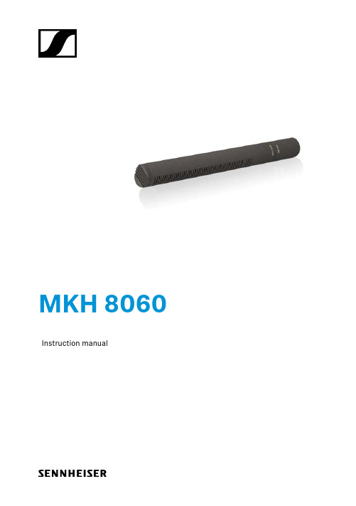
MKH 8060 产品说明书
MKH 8060 Instruction manualImportant safety instructions Important safety instructions1.Read these safety instructions and the instruction manual of the product.2.Keep these safety instructions and the instruction manual of the product.Always include all instructions when passing the product on to third parties.3.Only use attachments, accessories and spare parts specified by the manu-facturer.4.Caution: The protective basket and pop shield must be completely dry whenyou mount them on the microphone. Moisture can cause malfunctions or damage to the capsule.5.Connect the microphone only to microphone inputs and supply units thatprovide 48 V phantom powering in accordance with IEC 61938.6.Do not attempt to open the product housing on your own.7.Refer all servicing to qualified service personnel. Servicing is requiredwhen the product has been damaged in any way, liquid has been spilled or objects have fallen into the product, when the product has been exposed to rain or moisture, does not operate normally, or has been dropped.e the product only under the conditions of use listed in the specifications.9.Let the product come to ambient temperature before switching it on.10.Do not operate the product if it was damaged during transportation.11.Always run cables so that no one can trip over them.12.Keep the product and its connections away from liquids and electricallyconductive objects that are not necessary for operating the product.13.Do not use any solvents or aggressive cleaning agents to clean the product.14.Caution: Very high signal levels can damage your hearing and your loud-speakers. Reduce the volume on the connected audio devices beforeswitching on the product; this will also help prevent acoustic feedback. Intended useThe product is designed for indoor use.It is considered improper use when the product is used for any application not named in the corresponding instruction manual.Sennheiser does not accept liability for damage arising from improper use or misuse of this product and its attachments/accessories.Before putting the products into operation, please observe the respective country-specific regulations!MKH 8060MKH 8060Delivery includesDelivery includes•Microphone, consisting of the MKH 8060 microphone head and the MZX 8000 XLR module •MZQ 8060 microphone clamp •MZW 8060 foam windshield •Instruction manual •Frequency response sheet •Threaded transport tubeProduct overview11 Foam windshield2 Microphone head3 XLR module4 Microphone clamp (thread adaptor included for 3/8" and 5/8" threads)Putting the MKH 8060 into operation Putting the MKH 8060 into operation Connecting the microphoneConnection data of the MKH 8060:•48 V ±4 V phantom powering (P48, as per IEC 61938)•XLR-3 connector, balancedTo connect the MKH 8060 to a mixing console or recording device:f Connect the socket of the microphone cable to the microphone.f Connect the connector of the microphone cable to the mixing console orrecording device.Attaching the microphonef Select the suitable mounting thread:•Without thread insert: 5/8" thread•Thread insert: 3/8" threadf Screw the microphone clamp 4 to a stand.f Place the microphone with its back end into the microphone clamp: Makesure that the lateral slots are not covered.f Orient the microphone together with the microphone clamp and fix them byscrewing the wing screw tight.MKH 8060Using optional modulesTo suppress structure-borne noise, you can use one of the optional shockmounts.Sennheiser MZS 20-1 Sennheiser MZS 40Using the windshieldThe windshield changes the sound only slightly, but attenuates wind noise by approx. 25 dB.f Place the MZW 8060 foam windshield 1 over the microphone head 2 so thatall lateral slots are covered.Alternative windshields are available as accessories and can be found on the MKH 8060 product page at .Using optional modulesYou can retrofit and extend the microphones of the modular MKH 8000 micro-phone series by using optional modules.The MZF 8000 II filter moduleThe MZF 8000 II filter module has been specially designed for broadcast and film applications. It effectively filters out interference caused by infrasound, such a lowfrequency wind and handling noise.f If necessary, disconnect a connected XLR cable in order to not distort theMKH 8060Transporting the microphone cable and to avoid short-circuits.f Unscrew the microphone head 2 from the XLR module 3.f Screw the MZF 8000 II filter module 4 at a suitable place in the audio signalTransporting the microphonef Let the microphone dry if you used it under extreme climatic conditions.f If necessary, remove the windshield or take the microphone out of the basketwindshield.f Slide the microphone into the transport tube.MKH 8060Cleaning and maintaining the microphoneCleaning and maintaining the microphoneNOTICEDAMAGE TO THE PRODUCT DUE TO LIQUIDS!Liquids entering the product can short-circuit the electronics or damage the mechanics. Solvents or cleansing agents can damage the surface of the prod-uct.f Keep all liquids away from the product.f Only use a soft, slightly damp cloth to clean the product. SpecificationsPick-up pattern super-cardioid/lobarFrequency response50 Hz to 25,000 HzSensitivity-24 dBV/Pa (63 mV/Pa)Max. sound pressure level129 dB SPLEquivalent noise level A-weightedCCIR-weighted 11 dB(A) 23 dBNominal impedance25 ΩMin. terminating impedance 2 kΩPhantom powering48 V ± 4 V (P48, IEC 61938) Current consumption 3.3 mADiameter19 mmLengthwith MZX 8000 XLR module 145 mm 178 mWeightwith MZX 8000 XLR module 80 g 112 gOperating temperature-10 °C to +60 °CMKH 8060MKH 8060SpecificationsPolar pattern30°150°120°60°90°0510152025dB30°0°180°150°120°60°90°125 Hz 250 Hz 500 Hz 1,000 Hz2,000 Hz 4,000 Hz 8,000 Hz 16,000 HzFrequency response-10-20-30-40-50-60dB 90°0°50 H z100 H z200 H z500 H z1 k H z2 k H z5 k H z10 k H z20 k H zManufacturer declarationsManufacturer declarationsWarrantySennheiser electronic GmbH & Co. KG gives a warranty of 24 months on these products.For the current warranty conditions, please visit our website at or contact your Sennheiser partner.Warranty FOR AUSTRALIA and NEW ZEALAND ONLY:Sennheiser Australia Pty Ltd provides a warranty of 24 months on these products. For the current warranty conditions, visit Sennheiser website:Australia: https:///New Zealand: https:///Sennheiser goods come with guarantees that cannot be excluded under Aus-tralian and New Zealand Consumer law. You are entitled to a replacement or refund for a major failure and compensation for any other reasonably fore-seeable loss or damage. You are also entitled to have the goods repaired or replaced if the goods fail to be of acceptable quality and the failure does not amount to a major failure.This warranty is in addition to other rights or remedies under law. Nothing in this warranty excludes, limits or modifies any remedy available to be consumer which is granted by law.To make a claim under this contract, raise a case via Sennheiser website Australia: https:///service-support-contactNew Zealand: https:///service-support-contactAll expenses of claiming the warranty will be borne by the person making the claim.Sennheiser international warranty is provided by: Sennheiser Australia Pty Ltd (ABN 68 165 388 312) Level 14, Tower A Zenith Building, 821 Pacific Highway, Chatswood NSW 2067, AustraliaMKH 8060Manufacturer declarations In compliance with the following requirementsEU: UK:• WEEE Directive (2012/19/EU)•WEEE Regulations (2013)Notes on disposalThe symbol of the crossed-out dumpster on the product, the (rechargeable) battery (if applicable) and/or the packaging indicates that these products must not be disposed of with normal household waste, but must be disposed of sep-arately at the end of their service life. For the packaging, follow the regulations in your country for separating waste. Improper disposal of packaging materials can be harmful to your health and the environment.The separate collection of waste electrical and electronic equipment, (re-chargeable) batteries (if applicable) and packaging is intended to promote reuse and recycling and to prevent negative impacts on public health and the environment, for example due to hazardous substances contained in these products. At the end of their service life, recycle electrical and electronic equipment and (rechargeable) batteries so that their materials can be reused and to prevent environmental pollution.If (rechargeable) batteries can be removed without destroying them, you are obliged to dispose of them separately (see the product’s operating instructions for information on how to remove the batteries safely). Be especially careful when handling (rechargeable) batteries containing lithium, as these pose spe-cial hazards, such as the risk of fire and/or health risks if button cells are swal-lowed. Reduce battery waste as much as possible by using longer-life batteries or rechargeable batteries.Further information on the recycling of these products can be obtained from your municipal administration, from the municipal collection points, or from your Sennheiser partner. You may also be able to return electrical or electronic equipment to your distributor, if they are legally required to do so. By dispos-ing of your batteries properly, you are helping to protect public health and the environment.MKH 8060Manufacturer declarationsUK Declaration of conformity•RoHS Regulations (2012)•EMC Regulations (2016)Importer: Sennheiser UK Ltd.Pacific House, Third Avenue, Globe Park, MarlowBuckinghamshire SL7 1EY, United KingdomEU Declaration of conformity•RoHS Directive (2011/65/EU)•EMC Directive (2014/30/EU)The full text of the EU declaration of conformity is available at the following internet address: /download.Statements regarding the FCC and Industry Ca-nada rulesThis device complies with part 15 of the FCC rules. Operation is subject to the following two conditions: (1) this device may not cause harmful interference, and (2) this device must accept any interference received, including interfer-ence that may cause undesired operation.Contact information:Sennheiser Electronic Corporation1 Enterprise Drive, Old Lyme, CT 06371MKH 8060Compliance ComplianceEuropeUKUSA FCC 47 CFR 15 subpart BCanada Industry Canada CAN ICES-003(B) /Australia/New ZealandVietnam Kể từ ngày 1 tháng 12 năm 2012, các sảnphẩm được sản xuất bởi Sennheiser tuânthủ Thông tư 30/2011/TT-BCT quy định vềgiới hạn cho phép đối với một số chất độchại trong các sản phẩm điện và điện tử.MKH 8060Sennheiser electronic GmbH & Co. KGAm Labor 1, 30900 Wedemark, Germany, Printed in Germany, Publ. 07/23, 581394/A04。
- 1、下载文档前请自行甄别文档内容的完整性,平台不提供额外的编辑、内容补充、找答案等附加服务。
- 2、"仅部分预览"的文档,不可在线预览部分如存在完整性等问题,可反馈申请退款(可完整预览的文档不适用该条件!)。
- 3、如文档侵犯您的权益,请联系客服反馈,我们会尽快为您处理(人工客服工作时间:9:00-18:30)。
Varactor-Tuned Oscillators Technical DataVTO-8000 SeriesPin ConfigurationTO-8VFeatures•600 MHz to 10.5 GHz Coverage •Fast Tuning•+7 to +13 dBm Output Power •±1.5 dB Output Flatness •Hermetic Thin-film Construction+V DescriptionHP VTO-8000 Series oscillators use a silicon transistor chip as a negative resistance oscillator. The oscillation frequency is deter-mined by a silicon abrupt varactor diode acting as a voltage-variable capacitor in a thin-film micro-stripline resonator. This provides extremely fast tuning speed,limited primarily by the internal impedance of the user-supplied voltage driver. Fast settling is another feature of the HP VTO-8000 Series oscillators.Typical settling times for theVTO-8090 are <200␣kHz within one microsecond while the VTO-8950settles to <2␣MHz within two microseconds referenced to ten milliseconds. The VTO-8850combines a bipolar transistor oscillator with a GaAs FET buffer stage. This GaAs FET buffer isolates the oscillator fromvariations in load impedance for low frequency pulling, allows the oscillator to run lighty-loaded for low phase noise content and provides +10 dBm of minimum output power over the full tuning range. The VTO-8000 Series varactor-tuned oscillators are packaged in TO-8 transistor cans for simple installation in a conventional 50-ohm micro-stripline PC board. They are ideal for most compact, lightweight commercial and military equip-ment designs. Test fixturing is also available for lab bench test applications. See the “Test Fixtures for TO-8 Packages”section for additional information and outlines.ApplicationsFrequency agile systems, such as digitally controlled receivers and active jamming transmitters often use externally linearizedvaractor-tuned oscillators. HP oscillators are monotonic making external linearization easy using analog (opamp) or digital(EPROM) linearizing techniques.The HP VTO Series has been designed with a tuning input bypass capacitance which is sufficient to provide the neces-sary RF filtering action yet as lowas possible to maximize ∆V/∆T characteristics for excellent tuning speeds. Used in a phase locked loop PLL circuit, a VTO provides a receiver LO with stability equivalent to the refer-ence oscillator (usually crystal controlled), yet variable in discrete steps or continuously depending on the PLL configuration.Another important aspect of VTOs used in an LO application is their power vs. frequency flatness(±1.5␣dB). This assures that once a receiver mixer is biased for best dynamic range the local oscillator drive will remain constant throughout the tuning range without complex leveling circuitry.Electrical and Performance SpecificationsGuaranteed Specifications @ 25°C Case Temperature (0° to +65°C Operating Temperature)Part Number VTO–8060VTO–8080VTO–8090VTO–8150VTO–8200 Frequency Range, Min.600–1000 M Hz800–1400 M Hz900–1600 M Hz1500–2500 M Hz2000–3000 M Hz Power Output into 50–ohm Load,Min.20 mW/+13 dBm20 mW/+13 dBm20 mW/+13 dBm10 mW/+10 dBm10 mW/+10 dBm Power Output Variation @ 25°C, Max.±1.5 d B±1.5 d B±1.5 d B±1.5 d B±1.5 d B Operating Case Temperature Range0° to +65°C0° to +65°C0° to +65°C0° to +65°C0° to +65°C Frequency Drift Over Operating8 M Hz10 M Hz10 M Hz18 M Hz30 M Hz Temperature, Typ.Pulling Figure (12 dB Return Loss), Typ.25 MHz25 MHz25 MHz35 MHz35 MHz Pushing Figure, +15 VDC Supply, Typ. 5 M Hz/V 6 M Hz/V 6 M Hz/V 6 M Hz/V 6 M Hz/V Harmonics, Below Carrier, Typ.–15 dB–15 dB–15 dB–15 dB–18 dB Spurious Output Below Carrier, M in.–60 dB–60 dB–60 dB–60 dB–60 dB Tuning VoltageLow Frequency3±1 V DC2±1.5 V DC2±1 V DC 2.5±1 V DC2+2/–1 VDC High Frequency40±8 V DC35±10 V DC48+8/–10 V DC47±8 V DC20±4 V DC Maximum Tuning Voltage+60 V DC+60 V DC+60 V DC+60 V DC+45 V DC Tuning Port Capacitance, Nom.180 pF180 pF180 pF90 pF45 pF Phase Noise, Singie Sideband,1 Hz Bandwidth, Typ.50 kHz From Carrier–110 dBc/Hz–100 dBc/Hz–100 dBc/Hz–95 dBc/Hz–95 dBc/Hz100 kHz From Carrier–117 dBc/Hz–107 dBc/Hz–107 dBc/Hz–102 dBc/Hz–102 dBc/Hz Input Power ±1% RegulationVoltage, Nom.+15 V DC+15 V DC+15 V DC+15 V DC+15 V DC Current, Max.50 mA50 mA50 mA50 mA50 mA Case Style TO–8V TO–8V TO–8V TO–8V TO–8V Part Number VTO–8240VTO-8360VTO–8430VTO–8580 Frequency Range, Min.2400–3700 M Hz3600–4300 M Hz4300–5800 M Hz5800–6600 M Hz Power Output Into 50–ohm Load, Min.10 mW/+10 dBm10 mW/+10 dBm10 mW/+10 dBm 5 mW/+7 dBm Power Output Variation @25°C., Max.±1.5 d B±1.5 d B±1.5 d B±1.5 d B Operating Case Temperature Range0° to +65°C0° to +65°C0° to +65°C0° to +65°C Frequency Drift Over Operating30 M Hz35 M Hz60 M Hz70 M Hz Temperature, Typ.Pulling Figure (12 dB Return Loss), Typ.35 MHz40 MHz50 MHZ70 MHz Pushing Figure, +15 VDC Supply, Typ. 6 M Hz/V 6 M Hz/V 6 M Hz/V8 M Hz/V Harmonics, Below Carrier, Typ.–18 dB–25 dB–25 dB–25 dB Spurious Output Below Carrier, Min.–60 dB–60 dB–60 dB–60 dB Tuning VoltageLow Frequency2+2/–1 VDC8±2 V DC 1.0 VDC Min5±2.5 V DC High Frequency30±8 V DC24±4 V DC20.0 VDC M ax.24+3/–5 VDC Maximum Tuning Voltage+45 V DC+30 V DC+30 V DC+30 V DC Tuning Port Capacitance, Nom.45 pF45 pF45 pF45 pF Phase Noise, Single Sideband,1 Hz Bandwidth, Typ.50 kHz From Carrier–95 dBc/Hz–100 dBc/Hz–90 dBc/Hz–85 dBc/Hz100 kHz From Carrier–102 dBc/Hz–108 dBc/Hz–97 dBc/Hz–92 dBc/Hz Input Power ±1% RegulationVoltage, Nom.+15 V DC+15 V DC+15 V DC+15 V DC Current, Max.50 mA50 mA50 mA50 mACase Style TO–8V TO–8V TO–8V TO–8VElectrical and Performance SpecificationsGuaranteed Specifications @ 25°C Case Temperature (0° to +65°C Operating Temperature)Part Number VTO–8650VTO–8810VTO–8850VTO–8950 Frequency Range, Min.6500-8600 M Hz8100–9100 M Hz8500–9600 M Hz9500–10500 M Hz Power Output Into 50–ohm load, Min.10 mW/+10 dBm10 mW/+10 dBm10 mW/+10 dBm10 mW/+10 dBm Power Output Variation @ 25°C., Max.±1.5 d B±1.5 d B±1.5 d B±1.5 d B Operating Case Temperature Range0° to +65°C0° to +65°C0° to +65°C0° to +65°C Frequency Drift Over Operating100 M Hz110 M Hz110 M Hz160 M Hz Temperature, Typ.Pulling Figure (12 dB Return Loss), Typ.15 MHz8 MHz10 MHz20 MHz Pushing Figure, +15 VDC Supply, Typ.10 M Hz/V12 M Hz/V15 M Hz/V10 M Hz/V Harmonics, Below Carrier, Typ.–20 dB–15 dB–25 dB–20 dB Spurious Output Below Carrier, Min.–60 dB–60 dB–60 dB–60 dB Tuning VoltageLow Frequency2±1 V DC 2 VDC Min.5±2 V DC4±1 V DC High Frequency20±5 V DC16 VDC Max.13±5 V DC10 VDC Max. Maximum Tuning Voltage30 VDC+30 V DC+30 V DC+15 V DC Tuning Port Capacitance, Nom.26 pF26 pF26 pF26 pF Phase Noise, Single Sideband,1 Hz Bandwldth, Typ.50 kHz From Carrier–80 dBc/Hz–80 dBc/Hz–82 dBc/Hz–73 dBc/Hz100 kHz From Carrier–88 dBc/Hz–88 dBc/Hz–90 dBc/Hz–80 dBc/Hz Input Power ±1% RegulationVoltage, Nom.+15 V DC+15 V DC+15 V DC+15 V DC Current, M ax.50 mA100 mA100 mA100 mA Case Style TO–8V TO–8V TO–8V TO–8V SchematicRF OutputV TuneTypical Performance @ 25ºC Case TemperatureTypical Performance (Continued)–20L O G £(f ), d B c /H z1kFigure 14. Noise Comparison Single Sideband Phase Noise.FOURIER FREQUENCY, Hz10k 100k 1M –40–60–80–100–120–140–16010MFigure 13. VTO–8950 Power Output, Frequency and Modulation Sensitivity vs. Tuning Voltage.131211121098024681002004006008001011121416F R E Q U E N C Y ,GH zTUNING VOLTAGE, VDCP O W E R O U T P U T , d B mM O D U L A T I O N S E N S I T I V I T Y , M H z /VTO-8V Case DrawingAPPROXIMATE WEIGHT 1.7 GRAMSOUT(3X)NOTES (UNLESS OTHERWISE SPECIFIED):1. DIMENSIONS ARE SPECIFIED IN INCHES 2. TOLERANCES: xx ± .02xxx ± .010Test Fixtures for TO-8␣Packages (TF 801/802)Oscillators (VTO)Features•DC to 11 GHz Frequency Range •Connectorized Tuning Port and RF Output •Easy to Test Package •Repeatable PerformanceApplications•EngineeringCharacterization •Incoming Inspection •System Prototype •Demonstration of Device PerformanceDescriptionTo facilitate testing andprototyping of products in the TO-8V package, a series of test fixtures is available. Designated the HP TF Series test fixtures,they feature rugged construction for precise, repeatable measurements.The TF Series test fixtures come supplied with mounting hardware to ensure excellent ground contact between the oscillator package and test fixture. Thisassures excellent contact between package pins and test fixtureconnector pins for reliable testing.The device under test is aligned according to Figure 15, and pushed fully down onto the fixture. The steel mounting ringclamp is placed over the device under test and secured by ma-chine screws prior to testing.Orientation of pins can be verified by comparison with part (c) of Figure 15. It is recommended that both machine screws be used to fasten the ring clamp. Screws should be tightened down snugly with a jewelers type screwdriver.For different connector options check the table in Figure 15 to identify the correct part numbers.It should be noted that some output power variation may be seen, from unit data, at frequen-cies above 8 GHz. This isdue to small differences in lengths of test fixture RF output connector pins.Figure 15. TO-8 Test Fixture.TYP(Bottom View)GROUND(c)TUNING VOLTAGE (b)(a)CONNECTOR OPTIONSSERIES TF-801TF-802TUNING VOLTAGE SMA SMARF OUTPUT SMA TYPE N。