106773-1中文资料
DB34T 1757-2012 黄山白茶.pdf
ICS67.140.10X 55 DB34 安徽省地方标准DB 34/T 1757—2012安徽省质量技术监督局发布DB34/T 1757—2012前言本标准按照 GB/T 1.1-2009 给出的规则起草。
本标准由歙县质量技术监督局、歙县科技局、黄山甘白香白茶生态园共同提出。
本标准由安徽省农业标准化技术委员会归口。
本标准主要起草单位:黄山甘白香白茶生态园、黄山新安玉芽有机白茶专业合作社、歙县质量技术监督局、歙县科技局、歙县茶产业发展办公室、歙县茶叶行业协会。
本标准主要起草人:曹月红、江稳华、孙小勇、毕小卫、方维国、凌睿、夏南生、曹卿、张俭熟。
IDB34/T 1757—2012黄山白茶1 范围本标准规定了黄山白茶的术语和定义、产品分类与等级、要求、试验方法、检验规则以及标志标签、包装、运输和贮存。
本标准适用于安徽省黄山市行政区划范围内生产的黄山白茶。
2 规范性引用文件下列文件对于本文件的应用是必不可少的。
凡是注日期的引用文件,仅所注日期的版本适用于本文件。
凡是不注日期的引用文件,其最新版本(包括所有的修改单)适用于本文件。
GB/T 191 包装储运图示标志GB 2762 食品中污染物限量GB 2763 食品中农药最大残留限量GB 7718 食品安全国家标准 预包装食品标签通则GB/T 8302 茶 取样GB/T 8304 茶 水分测定GB/T 8305 茶 水浸出物测定GB/T 8306 茶 总灰分测定GB/T 8311 茶 粉末和碎茶含量测定GB/T 8314 茶 游离氨基酸总量测定GB/T 14487 茶叶感官审评术语GB 14881 食品企业通用卫生规范GB/T 18795 茶叶标准样品制备技术条件GB/T 23776 茶叶感官审评方法GB 28050 食品安全国家标准 预包装食品营养标签通则JJF 1070 定量包装商品净含量计量检验规则SB/T 10035 茶叶销售包装通用技术条件SB/T 10037 红茶、绿茶、花茶 运输包装DB34/T 773 清洁茶生产加工技术规范定量包装商品计量监督管理办法 国家质量监督检验检疫总局[2005]第75号令3 术语和定义下列术语和定义适用于本文件。
T-BERD 2207用户指南说明书
198150-15217-01Rev. DT-BERD 2207USER’S GUIDEThis manual applies to all T-BERD 2207 software incorporating software level 3.x.JANUARY 2000Copyright ©1998 TTC®USA 1-800-638-2049 • +1-301-353-1550 • FAX +1-301-353-0234Canada 1-888-689-2165 • +1-905-507-4117 • FAX +1-905-507-4126SECTION 9 - SpecificationsGeneral SpecificationsSECTION 9 SPECIFICATIONS9.1GENERAL SPECIFICATIONS9.1.1Physical Characteristics:Height:7.5" (19 cm)Width:11.5" (29.2 cm)Depth: 2.25" (5.7 cm)Weight: 4.25 lb. (1.93 kg.)9.1.2Environmental Characteristics:Temperature:Operating:32°F to 122°F (0°C to +50°C)Non-Operating:-40°F to 167°F (-40°C to +75°C)Humidity:10% to 90% Relative Humidity, non-condensing9.1.3Electrical Characteristics:Battery Type:10.8 V Nickel-Metal Hydride (NiMH)Operating Time:Typically, up to three hours of continuous operation on a full chargeRecharging Period:Maximum of two hours from full dischargeAC Adaptor:120VAC to 18 VDC 1.2A9.2DS1 SPECIFICATIONS9.2.1Input Specifications9.2.1.1RX JackConnector Type:Bantam jackFrequency:1,544,000 Hz ±5000 HzUser’s Guide T-BERD 22079-1SECTION 9 - SpecificationsDS1 SpecificationsImpedanceBRIDGE:1000 ohms minimumTERM:100 ohms ±5%DSX-MON:100 ohms ±5%RangeBRIDGE:+6 to -35.0 dBdsxTERM:+6 to -35.0 dBdsxDSX-MON:+6 to -24.0 dBdsx of resistive los9.2.1.2Loop Codes Detection CriteriaIn-Band:At least 177 error-free bits of the selected repetitive pattern must be received(loop up or loop down).Out-of-Band:Datalink monitored every 125 ms for loop codes (loop up and loop down).9.2.1.3Pattern Synchronization Detection CriteriaFixed Patterns:30 consecutive error-free bitsPseudo-random:30 + n consecutive error-free bits for a pattern length of 2^n-19.2.2Output Specifications9.2.2.1TX JackConnector Type:Bantam jackLBO Level:Line build-out of 0, -7.5, -15.0, and -22.5 dB of cable loss at 772 HzLBO Tolerance:±2 dB at 772 kHzTiming:±7 ppm internal or recoveredLine Codes:AMI or B8ZSError Insert Type:Logic, BP V, or FramePulse Shape:With output terminated in 100 ohms resistive load and 0 dB line build-outselected, the T-BERD 2207 meets ITU-T Recommendation G.703; AT&TPublications CB113, CB119, CB132, CB143, and PUB62508; and AT&TPUB62411 pulse shape specifications.9-2T-BERD 2207User’s GuideSECTION 9 - SpecificationsDS1 Specifications 9.2.2.2Transmitted Loop CodesIn-BandCSU:Loop-up: 10000; Loop-down: 100Facility 1:Loop-up: 1100; Loop-down: 1110Facility 2:Loop-up: 11000; Loop-down: 11100Facility 3:Loop-up: 100000; Loop-down: 100Out-of-BandLine:Loop up: 1111 1111 0111 0000Loop down: 1111 1111 0001 1100Payload:Loop up: 1111 1111 0010 1000Loop down: 1111 1111 0100 1100Network:Loop up: 1111 1111 0100 1000Loop down: 1111 1111 0010 01009.2.3Measurement SpecificationsFrequencyRange:1,544,000 ±5000 HzAccuracy:± 7 ppmResolution: 1 HzReceived LevelRange:+6 dBdsx to -40 dBdsxAccuracy:±1.0 dB between +6 and -10 dBdsx±2.0 dB between -10 and -20 dBdsx±3.0 dB between -20 and -40 dBdsxResolution:0.1 dBVp-p Range:60 mV to 12.0 VVp-p Resolution:0.05 VSimplex CurrentRange:10 mA to 180 mAccuracy:±5%Resolution: 1 mASimplex path:13.2 ohms (nominal)User’s Guide T-BERD 22079-3SECTION 9 - SpecificationsDS1 Specifications9.2.4Alarm CriteriaSignal Loss:175 ±75 consecutive zerosFrame LossD4: 2 out of 5 Ft bits in errorESF: 2 out of 5 frame bits in errorSLC-96: 2 out of 5 Ft bits in errorPattern Loss:100 errors detected in 1000 or fewer bitsOnes DensityQRSS:Alarm is suppressed.Other Patterns:Received data contains less than n ones in 8(n+1) bits, where n=1 to 23.Excess ZeroAMI:16 or more consecutive zerosB8ZS:8 or more consecutive zerosYellow AlarmD4:Bit 2 is a 0 for 255 consecutive channels.ESF:256 bits ±16 bits of a repetitive (1111 1111 0000 0000) pattern received inthe 4 kb/s datalink.SLC-96:Bit 2 is a 0 for 255 consecutive channels.AIS:Unframed T1 signal has 2048 consecutive ones.Low Battery:Battery has less than 25% energy remaining.9-4T-BERD 2207User’s GuideSECTION 9 - Specifications DS3 Option SpecificationsUser’s Guide T-BERD 22079-59.3DS3 OPTION SPECIFICATIONS9.3.1DS3 Specifications9.3.1.1Framing Formats9.3.1.2Patterns9.3.1.3Line Coding•B3ZS9.3.1.4Connectors•WECO 560A jack9.3.1.5Receiver (Single)Frequency:44,736 Mb/s ±300ppmLevel:HIGH: Accepts Nominal 1.2 Vp, 0 ft. of cable from High sourceDSX: Accepts Nominal 0.6 Vp, 450 ft. of c able from High source or monitor LOW: Accepts Nominal 0.3 Vp, 900 ft. of cable from High source9.3.1.6Transmitter (Single)Frequency:44,736 Mb/s ±20ppmPulse:HIGH: Nominal 1.2 Vp (Signal meets ANSI specification T1.102-1993 and ITU-TG.703 when subjected to 450 feet of cable loss.)•Auto• Muxed M13•Unframed • C-bit•M13• Muxed C-bit•1111• 215-1•1100 (Idle)• 220-1•1010 (AIS)• 223-1•1010• User (3 to 24 bit programmable)SECTION 9 - SpecificationsDS3 Option SpecificationsDSX: Nominal 0.91 Vp (Signal meets ANSI specification T1.102-1993 andITU-TG.703.)LOW: Nominal 0.31 VpTiming:Internal ClockRecovered Clock9.3.2DS3 Measurements9.3.2.1Summary•Bit Errors•Frame Errors•Bipolar Violations•Receive Frequenc•Parity Errors•FEAC Messages•C-bit Errors•DS2 Frame Errors•FEBE•Pattern Slip9.3.2.2Logic•Bit Errors•Pattern Slips•Bit Error Rate•Pattern Loss Seconds•Bit Errored Seconds•Error Free Seconds•Pattern Losses•% Error Free Seconds9.3.2.3Bipolar Violations•BPV•BPV Rate•BPV Errored Seconds9-6T-BERD 2207User’s GuideSECTION 9 - SpecificationsDS3 Option Specifications 9.3.2.4Frame Errors•Frame Error Rate•FEBE Rate•Frame Error Seconds•DS2 Frame Errors•Out of Frame Seconds•DS2 Frame Error Rate•C-bit Errors•Received X-bit•C-bit Error Rate•Transmit X-bit•FEBE•Frame Loss Count9.3.2.5Parity•Parity Errors•Parity Error Rate•Parity Error Seconds9.3.2.6Signal•Signal Loss•Signal Loss Seconds•Receive Frequency•Receive Signal Level•Transmit FrequencyUser’s Guide T-BERD 22079-7。
ISO 16047中英(优选.)

Fasteners-Torque/clamp force testing 紧固件 紧固扭矩-轴向预紧力试验
第 1 页 共 24 页
Contents 目录
1 Scope 范围 ............................................................................................................................................................................... 4 2 Normative references 引用标准 ........................................................................................................................................... 4 3 Terms and definitions 术语和定义....................................................................................................................................... 6
3.1 clamp force F 预紧力 ............................................................................................................................................ 6 3.2 yield clamp force Fy 屈服紧固轴力 ...................................................................................................................... 6 3.3 ultimate clamp force FU 极限紧固轴力................................................................................................................ 6 3.4 tightening torque T 紧固扭矩 ................................................................................................................................ 6 3.5 yield tightening torque Ty 屈服紧固扭矩 ............ 6 3.6 thread torque Tth 螺纹扭矩.................................................................................................................................. 6 3.7 bearing surface friction torque Tb 支承面摩擦扭矩 ....................................................................................... 7 3.8 ultimate tightening torque Tu 极限紧固扭矩.................................................................................................... 7 4 Symbols and their designations 符号和名称.................................................................................................................... 7 5 Principle of test 试验原理........................................................................................................................................................ 8 5.1 General 综述 ................................................................................................................................................................ 8 5.2 Determination of coefficients of friction 摩擦系数的测定 ................................................................................... 9 5.3 Determination of torque coefficient K (K-factor) 扭矩系数 K 的测定(K-指数)........................................... 10 5.4 Determination of ratio T/F T/F 比率的确定 ........................................................................................................ 10 6 Apparatus 设备 ...................................................................................................................................................................... 10 6.1 Testing machine 试验设备 ........................................................................................................................................ 10 6.2 Test fixture 试验工装................................................................................................................................................ 11 7 Test parts 试验零件 ................................................................................................................................................................. 12 7.1 General 综述 ................................................................................................................................................................ 12 7.2 Test-bearing plates or test washers 试验支承圆盘或试验垫片 ......................................................................... 12
技术数据10707(有效日期:2020年11月)说明书
Product features• 5 mm x 20 mm physical size • Fast-acting ceramic tube • 420 Vac rating• Nickel/silver plated brass end construction •Available in cartridge and axial leadEnvironmental complianceApplications• Data center server power supplies • Intelligent commercial buildings • T elecom power supplies•High-energy and power efficient applications (3-phase power supplies, inverters, and ballasts)Agency information• UR Recognition: File: E19180, Guide: JDYX2•TUV: T 50484820 02Catalog symbol•See page 4 for ordering codesS5205 mm x 20 mm Fast-acting ceramic tube fusesPackaging prefix• Blank 5 pieces in one case (5 in tin, only forcartridge version)• BK/ 100 pieces packed into a cardboard carton• BK1/ 1000 pieces packed into a polybag (only cartridge version)•TR2/ 1500pcs in one reel (only for axial lead version)Option code•-V- (Axial leads - copper tinned wire with nickel-plated brass end caps)BK/ S520- V- 12-5 - RPackaging prefixProduct code Option code Ampere ratingRoHS compliantPb HALOGENHF FREE2Technical Data 10707Effective November 2020S5205 mm x 20 mm Fast-acting ceramic tube fuses/electronicsElectrical characteristicsl n1.0l n min hours2.1l n max minutes2.75l n min seconds2.75l n max seconds4.0l n min seconds4.0l n max seconds10l n max ms8 A to 20 A 1300.04200.01130Product specificationsPart number 5 CartridgeAxial leadCurrent rating (A)Voltage rating (Vac)Interrupting rating 4 at 420/250 Vac (A)TypicalDC cold resistance 1 (mΩ )Typical melting 2 l 2t (A 2s)Typicalvoltage drop 3(mV)S520-8-R S520-V-8-R 8420200/150********S520-10-R S520-V-10-R 10420200/150********S520-12-5-R S520-V-12-5-R 12.5420300/15008.1160180S520-15-R S520-V-15-R 15420300/1500 6.8220195S520-16-R S520-V-16-R 16420300/1500 6.1280200S520-20-RS520-V-20-R20420300/15005420205Dimensions–mm1. Typical DC cold resistance measured at <10% of rated current2. Typical I 2t measured at 10In and rated voltage3. Typical voltage drop measured at +20 °C at rated current4. PF=1 for 420 Vac, PF= 0.7 to 0.8 for 250 Vac5. Part Number Definition: S520--x-xxx-R S520 = Product codex= Use “V” code for axial lead, leave blank for cartridgexxx = Ampere rating-R suffix = RoHS compliantDimension A (ref): 0.80 mm for 8 A to 10 A 1.00 mm for 12.5 A to 16 A 1.20 mm for 20 ADimension B:(BK) packaging- 38.1± 0.38 mm(TR2) packaging- 15.8 ± 2 mm3Technical Data 10707Effective November 2020S5205 mm x 20 mm Fast-acting ceramic tube fuses /electronics Time vs. current curveI 2t vs. time curve4Technical Data 10707Effective November 2020S5205 mm x 20 mm Fast-acting ceramic tube fuses/electronicsT emperature derating curveGeneral specificationsOperating temperature: -55 °C to +125 °C (with derating)Storage temperature: -55 °C to +125 °CHumidity Test: MIL-STD-202G Method 103B, 85% ±2% relative humidity @ +85 ±2 °C, 72 hours Thermal shock: MIL-STD-202G Method 107G air-to-air, -55 °C -125 °C, 100 cycles Mechanical shock: MIL-STD-202G Method 213 A, 50 g, 11 ms Vibration: MIL-STD-202, Method 204D, condition D, 20 g, 10 - 500 Hz Solderability: J-STD-002, Method A1Resistance to solder: MIL-STD-202, Method 210, +260 °C, 10 s Terminal strength: 10 NOrdering CodesThe ordering code is the Catalog part number replacing the “/” and “.” with a “-”When using the -V option code, the parentheses “(“ “)” are not used.Catalog part numberOrder part numberCatalog part numberOrder part numberBK/S520(-V)-8-R BK-S520(-V)-8-R S520-8-R S520-8-R BK/S520(-V)-10-R BK-S520(-V)-10-R S520-10-R S520-10-R BK/S520(-V)-12.5-R BK-S520(-V)-12-5-R S520-12.5-R S520-12-5-R BK/S520(-V)-15-R BK-S520(-V)-15-R S520-15-R S520-15-R BK/S520(-V)-16-R BK-S520(-V)-16-R S520-16-R S520-16-R BK/S520(-V)-20-R BK-S520(-V)-20-R S520-20-R S520-20-R BK1/S520(-V)-8-R BK1-S520(-V)-8-R TR2/S520-V-8-R TR2-S520-V-8-R BK1/S520(-V)-10-R BK1-S520(-V)-10-R TR2/S520-V-10-R TR2-S520-V-10-R BK1/S520(-V)-12.5-R BK1-S520(-V)-12-5-R TR2/S520-V-12.5-R TR2-S520-V-12-5-R BK1/S520(-V)-15-R BK1-S520(-V)-15-R TR2/S520-V-15-R TR2-S520-V-15-R BK1/S520(-V)-16-R BK1-S520(-V)-16-R TR2/S520-V-16-R TR2-S520-V-16-R BK1/S520(-V)-20-RBK1-S520(-V)-20-RTR2/S520-V-20-RTR2-S520-V-20-RF a c t o r o f R a t e d c u r r e n tTemperature in Degrees CEatonElectronics Division 1000 Eaton Boulevard Cleveland, OH 44122United States/electronics© 2020 EatonAll Rights Reserved Printed in USAPublication No. 10707 BU-MC17042November 2020Technical Data 10707Effective November 2020S5205 mm x 20 mm Fast-acting ceramic tube fuses Life Support Policy: Eaton does not authorize the use of any of its products for use in life support devices or systems without the express writtenapproval of an officer of the Company. Life support systems are devices which support or sustain life, and whose failure to perform, when properly used in accordance with instructions for use provided in the labeling, can be reasonably expected to result in significant injury to the user.Eaton reserves the right, without notice, to change design or construction of any products and to discontinue or limit distribution of any products. Eaton also reserves the right to change or update, without notice, any technical information contained in this bulletin.T e m p e r a t u r eTimeT T T T Wave solder profile (Axial lead only)Reference EN 61760-1:2006Profile featureStandard SnPb solderLead (Pb) free solderPreheat • Temperature min. (T smin )100 °C 100 °C • Temperature typ. (T styp )120 °C 120 °C • Temperature max. (T smax )130 °C 130 °C • Time (T smin to T smax ) (t s )70 seconds 70 seconds Δ preheat to max Temperature150 °C max.150 °C max.Peak temperature (T P )*235 °C – 260 °C 250 °C – 260 °C Time at peak temperature (t p )10 seconds max5 seconds max each wave 10 seconds max5 seconds max each wave Ramp-down rate~ 2 K/s min ~3.5 K/s typ ~5 K/s max ~ 2 K/s min ~3.5 K/s typ~5 K/s max Time 25 °C to 25 °C4 minutes4 minutesManual solder+350 °C (4-5 seconds by soldering iron), generally manual/hand soldering is not recommendedEaton is a registered trademark.All other trademarks are property of their respective owners.Follow us on social media to get the latest product and support information.。
MOLYVAN 822 NT 安全数据表说明书

液体。
化学品安全技术说明书产品类型化学名石油的钼dialkyldithiocarbamate在加工油。
GHSChina产品名称MOLYVAN® 822 NT供应商/ 制造商Vanderbilt Chemicals, LLC 30 Winfield Street Norwalk, CT 06855石油的钼dialkyldithiocarbamate在加工油。
29170别名物质用途编号本SDS适用于美国,加拿大,日本和欧盟以外的司法管辖区 - 本产品在美国,加拿大,日本和欧洲联盟注册为CAS#906665-74-5。
如果您有任何疑问,请致电Vanderbilt Global Services,LLC的产品风险经理。
润滑剂减摩剂CHEMTREC +1-800-424-9300 (24小时紧急)紧急电话号码供应商1-203-853-1400户外 美国美国CHEMTREC +1-703-527-3887 (24小时紧急)安全技术说明书根据 GB/ T 16483-2008 和 GB/ T 17519-2013危害水生环境一长期危险 - 类别 4危险性类别信号词警告危险性说明吞咽可能有害。
可能对水生生物造成长期持续有害影响。
防范说明预防措施避免释放到环境中。
事故响应如误吞咽: 如感觉不适,呼叫解毒中心或医生。
安全储存不适用。
废弃处置处置内装物/容器按照地方/区域/国家/国际规章。
其他危害没有已知信息。
GHS标签要素物质/混合物混合物用水冲洗口腔。
如有假牙请摘掉。
将患者转移到空气新鲜处,休息,保持利于呼吸的体位。
如物质已被吞下且患者保持清醒,可饮少量水。
如患者感到恶心就应停止,因为呕吐会有危险。
禁止催吐,除非有专业医疗人士指导。
如发生呕吐, 应保持头部朝下以避免呕吐物进入肺部。
如有害的健康影响持续存在或加重,应寻求医疗救治。
如有必要,呼叫中毒控制中心或就医。
切勿给失去意识者任何口服物。
波生坦杂质列表-标准品
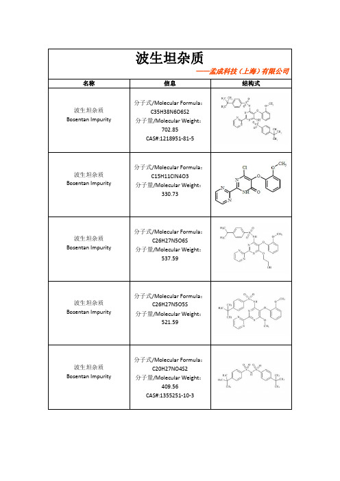
波生坦杂质——孟成科技(上海)有限公司名称信息结构式波生坦杂质Bosentan Impurity∙分子式/Molecular Formula :C35H38N6O6S2分子量/Molecular Weight :702.85CAS#:1218951-81-5波生坦杂质Bosentan Impurity ∙分子式/Molecular Formula :C15H11ClN4O3分子量/Molecular Weight :330.73波生坦杂质Bosentan Impurity ∙分子式/Molecular Formula :C26H27N5O6S分子量/Molecular Weight :537.59波生坦杂质Bosentan Impurity ∙分子式/Molecular Formula :C26H27N5O5S分子量/Molecular Weight :521.59波生坦杂质Bosentan Impurity ∙分子式/Molecular Formula :C20H27NO4S2分子量/Molecular Weight :409.56CAS#:1355251-10-3波生坦杂质Bosentan Impurity 分子式/Molecular Formula :C27H29N5O5S分子量/Molecular Weight :535.62波生坦杂质Bosentan Impurity ∙分子式/Molecular Formula :C25H24BrN5O4S分子量/Molecular Weight :570.46CAS#:1268849-14-4波生坦杂质Bosentan Impurity ∙分子式/Molecular Formula :C29H33N5O7S分子量/Molecular Weight :595.67CAS#:1257099-43-6波生坦杂质Bosentan Impurity ∙分子式/Molecular Formula :C27H27N5O5S分子量/Molecular Weight :533.60CAS#:1257099-44-7波生坦杂质Bosentan Impurity ∙分子式/Molecular Formula :C22H27N5O6S分子量/Molecular Weight :489.55CAS#:1257099-41-4波生坦杂质Bosentan Impurity ∙分子式/Molecular Formula :C20H21N5O4S分子量/Molecular Weight :427.48CAS#:1257099-42-5波生坦杂质Bosentan Impurity 分子式/Molecular Formula:C24H22ClN5O4S分子量/Molecular Weight:511.98CAS#:1268612-25-4波生坦杂质Bosentan Impurity ∙分子式/Molecular Formula:C15H12N4O4分子量/Molecular Weight:312.29CAS#:150728-12-4波生坦杂质Bosentan Impurity ∙分子式/Molecular Formula:C5H6N4.HCl分子量/Molecular Weight:158.59。
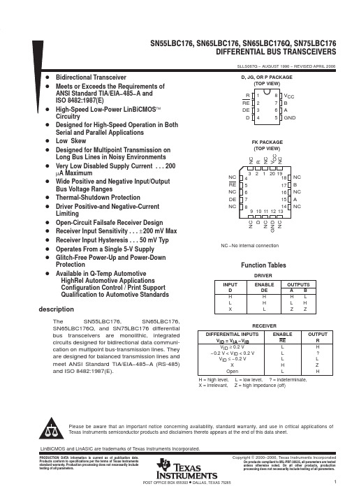
7LB176资料
PACKAGING INFORMATIONOrderable Device Status (1)Package Type Package Drawing Pins Package Qty Eco Plan (2)Lead/Ball FinishMSL Peak Temp (3)5962-9318301Q2A ACTIVE LCCC FK 201TBD POST-PLATE N /A for Pkg Type 5962-9318301QPA ACTIVE CDIP JG 81TBD A42SNPB N /A for Pkg Type SN65LBC176D ACTIVE SOIC D 875Green (RoHS &no Sb/Br)CU NIPDAU Level-1-260C-UNLIM SN65LBC176DG4ACTIVE SOIC D 875Green (RoHS &no Sb/Br)CU NIPDAU Level-1-260C-UNLIM SN65LBC176DR ACTIVE SOIC D 82500Green (RoHS &no Sb/Br)CU NIPDAU Level-1-260C-UNLIM SN65LBC176DRG4ACTIVE SOIC D 82500Green (RoHS &no Sb/Br)CU NIPDAU Level-1-260C-UNLIM SN65LBC176P ACTIVE PDIP P 850Pb-Free (RoHS)CU NIPDAU N /A for Pkg Type SN65LBC176PE4ACTIVE PDIP P 850Pb-Free (RoHS)CU NIPDAU N /A for Pkg Type SN65LBC176QD ACTIVE SOIC D 875TBD CU NIPDAU Level-1-220C-UNLIM SN65LBC176QDR ACTIVE SOIC D 82500TBD CU NIPDAU Level-1-220C-UNLIM SN75LBC176D ACTIVE SOIC D 875Green (RoHS &no Sb/Br)CU NIPDAU Level-1-260C-UNLIM SN75LBC176DG4ACTIVE SOIC D875Green (RoHS &no Sb/Br)CU NIPDAU Level-1-260C-UNLIM SN75LBC176DR ACTIVE SOIC D 82500Green (RoHS &no Sb/Br)CU NIPDAU Level-1-260C-UNLIM SN75LBC176DRG4ACTIVE SOIC D 82500Green (RoHS &no Sb/Br)CU NIPDAU Level-1-260C-UNLIM SN75LBC176P ACTIVE PDIP P 850Pb-Free (RoHS)CU NIPDAU N /A for Pkg Type SN75LBC176PE4ACTIVE PDIP P 850Pb-Free (RoHS)CU NIPDAUN /A for Pkg TypeSNJ55LBC176FK ACTIVE LCCC FK 201TBD POST-PLATE N /A for Pkg Type SNJ55LBC176JGACTIVECDIPJG81TBDA42SNPBN /A for Pkg Type(1)The marketing status values are defined as follows:ACTIVE:Product device recommended for new designs.LIFEBUY:TI has announced that the device will be discontinued,and a lifetime-buy period is in effect.NRND:Not recommended for new designs.Device is in production to support existing customers,but TI does not recommend using this part in a new design.PREVIEW:Device has been announced but is not in production.Samples may or may not be available.OBSOLETE:TI has discontinued the production of the device.(2)Eco Plan -The planned eco-friendly classification:Pb-Free (RoHS),Pb-Free (RoHS Exempt),or Green (RoHS &no Sb/Br)-please check /productcontent for the latest availability information and additional product content details.TBD:The Pb-Free/Green conversion plan has not been defined.Pb-Free (RoHS):TI's terms "Lead-Free"or "Pb-Free"mean semiconductor products that are compatible with the current RoHS requirements for all 6substances,including the requirement that lead not exceed 0.1%by weight in homogeneous materials.Where designed to be soldered at high temperatures,TI Pb-Free products are suitable for use in specified lead-free processes.Pb-Free (RoHS Exempt):This component has a RoHS exemption for either 1)lead-based flip-chip solder bumps used between the die and package,or 2)lead-based die adhesive used between the die and leadframe.The component is otherwise considered Pb-Free (RoHS compatible)as defined above.Green (RoHS &no Sb/Br):TI defines "Green"to mean Pb-Free (RoHS compatible),and free of Bromine (Br)and Antimony (Sb)based flame retardants (Br or Sb do not exceed 0.1%by weight in homogeneous material)(3)MSL,Peak Temp.--The Moisture Sensitivity Level rating according to the JEDEC industry standard classifications,and peak solder12-Jan-2007temperature.Important Information and Disclaimer:The information provided on this page represents TI's knowledge and belief as of the date that it is provided.TI bases its knowledge and belief on information provided by third parties,and makes no representation or warranty as to the accuracy of such information.Efforts are underway to better integrate information from third parties.TI has taken and continues to take reasonable steps to provide representative and accurate information but may not have conducted destructive testing or chemical analysis on incoming materials and chemicals.TI and TI suppliers consider certain information to be proprietary,and thus CAS numbers and other limited information may not be available for release.In no event shall TI's liability arising out of such information exceed the total purchase price of the TI part(s)at issue in this document sold by TI to Customer on an annualbasis.12-Jan-2007IMPORTANT NOTICETexas Instruments Incorporated and its subsidiaries (TI) reserve the right to make corrections, modifications, enhancements, improvements, and other changes to its products and services at any time and todiscontinue any product or service without notice. Customers should obtain the latest relevant informationbefore placing orders and should verify that such information is current and complete. All products are soldsubject to TI’s terms and conditions of sale supplied at the time of order acknowledgment.TI warrants performance of its hardware products to the specifications applicable at the time of sale inaccordance with TI’s standard warranty. Testing and other quality control techniques are used to the extentTI deems necessary to support this warranty. Except where mandated by government requirements, testingof all parameters of each product is not necessarily performed.TI assumes no liability for applications assistance or customer product design. Customers are responsiblefor their products and applications using TI components. To minimize the risks associated with customerproducts and applications, customers should provide adequate design and operating safeguards.TI does not warrant or represent that any license, either express or implied, is granted under any TI patentright, copyright, mask work right, or other TI intellectual property right relating to any combination, machine,or process in which TI products or services are used. Information published by TI regarding third-partyproducts or services does not constitute a license from TI to use such products or services or a warranty orendorsement thereof. Use of such information may require a license from a third party under the patents orother intellectual property of the third party, or a license from TI under the patents or other intellectualproperty of TI.Reproduction of information in TI data books or data sheets is permissible only if reproduction is withoutalteration and is accompanied by all associated warranties, conditions, limitations, and notices.Reproduction of this information with alteration is an unfair and deceptive business practice. TI is notresponsible or liable for such altered documentation.Resale of TI products or services with statements different from or beyond the parameters stated by TI forthat product or service voids all express and any implied warranties for the associated TI product or serviceand is an unfair and deceptive business practice. TI is not responsible or liable for any such statements.Following are URLs where you can obtain information on other Texas Instruments products and applicationsolutions:Products ApplicationsAmplifiers Audio /audioData Converters Automotive /automotive/broadbandBroadbandDSP DigitalControl /digitalcontrol Interface Military /military Logic Power Mgmt Optical Networking /opticalnetworkSecurity /security Microcontrollers Low Power Wireless /lpw Telephony /telephonyVideo & Imaging /video/wirelessWirelessMailing Address: Texas InstrumentsPost Office Box 655303 Dallas, Texas 75265Copyright © 2007, Texas Instruments Incorporated。
100371中文资料
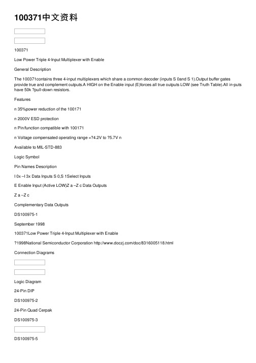
100371中⽂资料100371Low Power Triple 4-Input Multiplexer with EnableGeneral DescriptionThe 100371contains three 4-input multiplexers which share a common decoder (inputs S 0and S 1).Output buffer gates provide true and complement outputs.A HIGH on the Enable input (E)forces all true outputs LOW (see Truth Table).All in-puts have 50k ?pull-down resistors.Featuresn 35%power reduction of the 100171n 2000V ESD protectionn Pin/function compatible with 100171n Voltage compensated operating range =?4.2V to ?5.7V nAvailable to MIL-STD-883Logic SymbolPin Names DescriptionI 0x –I 3x Data Inputs S 0,S 1Select InputsE Enable Input (Active LOW)Z a –Z c Data OutputsZ a –Z cComplementary Data OutputsDS100975-1September 1998100371Low Power Triple 4-Input Multiplexer with Enable1998National Semiconductor Corporation /doc/8316005118.htmlConnection DiagramsLogic Diagram24-Pin DIPDS100975-224-Pin Quad CerpakDS100975-3DS100975-5/doc/8316005118.html2Truth TableInputs OutputsE S0S1Z nL L L I0xL H L I1xL L H I2xL H H I3xH X X LH=HIGH Voltage LevelL=LOW Voltage LevelX=Don’t Care3/doc/8316005118.htmlAbsolute Maximum Ratings (Note 1)If Military/Aerospace specified devices are required,please contact the National Semiconductor Sales Office/Distributors for availability and specifications.Storage Temperature (T STG )65C to +150C Maximum Junction Temperature (T J )Ceramic+175?CV EE Pin Potential to Ground Pin ?7.0V to +0.5V Input Voltage (DC)V EE to +0.5VOutput current (DC Output HIGH)?50mA ESD (Note 2)≥2000VRecommended Operating ConditionsCase Temperature (T C )Military55C to +125C Supply Voltage (V EE )5.7V to 4.2VNote 1:Absolute maximum ratings are those values beyond which the de-vice may be damaged or have its useful life impaired.Functional operation under these conditions is not implied.Note 2:ESD testing conforms to MIL-STD-883,Method 3015.Military VersionDC Electrical CharacteristicsV EE =?4.2V to ?5.7V,V CC =V CCA =GND,T C =?55?C to +125?C Symbol Parameter Min Max Units T C Conditions NotesV OHOutput HIGH Voltage1025870mV 0C to (Notes 3,4,5)+125?C ?1085870mV 55C V IN =V (Max)Loading with V OLOutput LOW Voltage18301620mV 0C to or V IL (Min)50?to ?2.0V+125?C ?18301555mV ?55?C V OHCOutput HIGH Voltage1035mV 0C to (Notes 3,4,5)+125?C ?1085mV ?55?C V IN =V IH (Min)Loading with V OLCOutput LOW Voltage1610mV 0C to or V IL (Max)50?to ?2.0V+125?C ?1555mV ?55?C V IH Input HIGH Voltage ?1165?870mV ?55?C to Guaranteed HIGH Signal (Notes 3,4, 5,6)+125?C for All InputsV IL Input LOW Voltage ?1830?1475mV ?55?C to Guaranteed LOW Signal (Notes 3,4,5,6)+125?C for All Inputs I IL Input LOW Current 0.50µA55C to V EE =4.2V (Notes 3,4,5)+125?CV IN =V IL (Min)I IHInput HIGH Current(Notes 3,4,5)I 0X –I 3X 340µA0?C to S 0,S 1,E 300+125?C V EE =?5.7V I 0X –I 3X 490µA ?55?CV IN =V IH (Max)S 0,S 1,E450I EEPower Supply Current8030mA55C to Inputs Open(Notes 3,4,5)+125?CNote 3:F100K 300Series cold temperature testing is performed by temperature soaking (to guarantee junction temperature equals ?55?C),then testing immediately without allowing for the junction temperature to stabilize due to heat dissapation after power-up.This provides “cold start”specs which can be considered a worst case condition at cold temperatures.Note 4:Screen tested 100%on each device at ?55?C,+25?C,and +125?C,Subgroups 1,2,3,7,and 8.Note 5:Sample tested (Method 5005,Table I)on each manufactured lot at ?55?C,+25?C,and +125?C,Subgroups 1,2,3,7,and 8.Note 6:Guaranteed by applying specified input condition and testing V OH /V OL ./doc/8316005118.html4Military VersionAC Electrical CharacteristicsV EE =?4.2V to ?5.7V,V CC =V CCA =GND Symbol ParameterT C =?55?C T C =+25?C T C =+125?C UnitsConditionsNotesMin Max Min Max Min Max t PLH Propagation Delay 0.101.900.201.700.202.00ns(Notes 7,8,9,11)t PHL I 0x –I 3x to Output t PLH Propagation Delay 0.402.700.602.400.502.90nst PHL S 0,S 1to Output Figures 1,2t PLH Propagation Delay 0.502.700.602.400.502.90nst PHL E to Output t TLH Transition Time0.201.600.301.500.201.60ns(Note 10)t THL20%to 80%,80%to 20%Note 7:F100K 300Series cold temperature testing is performed by temperature soaking (to guarantee junction temperature equals ?55?C),then testing immediately after power-up.This provides “cold start”specs which can be considered a worst case condition at cold temperatures.Note 8:Screen tested 100%on each device at +25?C temperature only,Subgroup A9. Note 9:Sample tested (Method 5005,Table I)on each mfg.lot at +25?C,Subgroup A9,and at +125?C and ?55?C temperatures,Subgroups A10and A11.Note 10:Not tested at +25?C,+125?C and ?55?C temperature (design characterization data).Note 11:The propagation delay specified is for single output switching.Delays may vary up to 300ps with multiple outputs switching.Test CircuitryDS100975-6Notes:V CC ,V CCA =+2V,V EE =?2.5VL1and L2=equal length 50?impedance lines R T =50?terminator internal to scopeDecoupling 0.1µF from GND to V CC and V EE All unused outputs are loaded with 50?to GND C L =Fixture and stray capacitance ≤3pFPin numbers shown are for flatpak;for DIP see logic symbolFIGURE 1.AC Test Circuit/doc/8316005118.html5Switching WaveformsDS100975-7FIGURE2.Propagation Delay and Transition Times /doc/8316005118.html6Physical Dimensions inches(millimeters)unless otherwise noted24-Lead Ceramic Dual-In-Line Package(D)Package Number J24E24-Lead Ceramic Flatpak(F)Package Number W24B7/doc/8316005118.htmlLIFE SUPPORT POLICYNATIONAL’S PRODUCTS ARE NOT AUTHORIZED FOR USE AS CRITICAL COMPONENTS IN LIFE SUPPORT DE-VICES OR SYSTEMS WITHOUT THE EXPRESS WRITTEN APPROVAL OF THE PRESIDENT OF NATIONAL SEMI-CONDUCTOR CORPORATION.As used herein:1.Life support devices or systems are devices or sys-tems which,(a)are intended for surgical implant intothe body,or (b)support or sustain life,and whose fail-ure to perform when properly used in accordancewith instructions for use provided in the labeling,can be reasonably expected to result in a significant injury to the user.2.A critical component in any component of a life support device or system whose failure to perform can be rea-sonably expected to cause the failure of the life support device or system,or to affect its safety or effectiveness.National Semiconductor Corporation AmericasTel:1-800-272-9959Fax:1-800-737-7018Email:support@/doc/8316005118.html/doc/8316005118.htmlNational Semiconductor EuropeFax:+49(0)180-5308586Email:europe.support@/doc/8316005118.htmlDeutsch Tel:+49(0)180-5308585English Tel:+49(0)180-5327832Fran?ais Tel:+49(0)180-5329358Italiano Tel:+49(0)180-5341680National Semiconductor Asia Pacific Customer Response Group Tel:65-2544466Fax:65-2504466Email:sea.support@/doc/8316005118.htmlNational Semiconductor Japan Ltd.Tel:81-3-5620-6175Fax:81-3-5620-6179100371L o w P o w e r T r i p l e 4-I n p u t M u l t i p l e x e r w i t h E n a b l eNational does not assume any responsibility for use of any circuitry described,no circuit patent licenses are implied and National reserves the right at any time without notice to change said circuitry and specifications.。
危险化学品理化性质及危险特性表

表7。
6—1苯的理化性质及危险特性表表7.6—7粗苯的理化性质及危险特性表表7。
6—82-丁氧基乙醇的理化性质及危险特性表表7。
6—111,4-二甲苯的理化性质和危险特性表表7。
6-12二甲苯异构体混合物的理化性质及危险特性表表7.6-14 二甲醚的理化性质及危险特性表7。
6—15 二甲氧基甲烷的理化性质及危险特性表7.6-16 1,2—二乙基苯的理化性质及危险特性表7.6—22 环辛烷的理化性质及危险特性表7。
6—23 1,2-环氧丙烷的理化性质及危险特性表7.6-24 环氧乙烷的理化性质及危险特性表7。
6-25甲苯的理化性质及危险特性表表7。
6—26甲醇的理化性质及危险特性表表7。
6—272-甲基-1-丙醇的理化性质及危险特性表表7。
6—28 2—甲基-2—丙醇的理化性质及危险特性表7.6-29 2—甲基丁烷的理化性质及危险特性表7。
6—30甲基叔丁基醚的理化性质及危险特性表表7。
6—31 甲醛溶液的理化性质及危险特性表7.6-32 煤焦沥青的理化性质及危险特性表7。
6-33 煤油的理化性质及危险特性表7。
6-36 溶剂苯的理化性质及危险特性表7。
6—37 溶剂油的理化性质及危险特性表7。
6—381,2,3-三甲基苯的理化性质及危险特性表表7.6—41石脑油的理化性质及危险特性表表7.6-42石油醚的理化性质及危险特性表7。
6-43 石油原油的理化性质及危险特性表7.6-44叔丁基苯的理化性质及危险特性表表7.6—451,2,4,5-四甲苯的理化性质及危险特性表表7。
6—46松焦油的理化性质及危险特性表7。
6-47 天然气的理化性质及危险特性表7。
6—48 液化石油气的理化性质及危险特性表7。
6-49乙苯的理化性质及危险特性表表7。
6—50 异丁烯的理化性质及危险特性表7。
6—51异辛烷的理化性质及危险特性。
