IRF840A说明书
IRF840中文资料_数据手册_参数
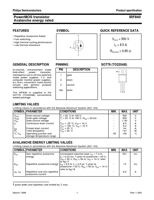
tf
Turn-off fall time
VDD = 250 V; RD = 30 Ω; RG = 9.1 Ω
Ld
Internal drain inductance Measured from tab to centre of die
Ld
Internal drain inductance Measured from drain lead to centre of die
CONDITIONS in free air
MIN. TYP. MAX. UNIT
-
- 0.85 K/W
- 60 - K/W
ELECTRICAL CHARACTERISTICS
Tj = 25 ˚C unless otherwise specified SYMBOL PARAMETER
CONDITIONS
SYMBOL PARAMETER
CONDITIONS
EAS EAR IAS, IAR
Non-repetitive avalanche energy
Unclamped inductive load, IAS = 7.4 A; tp = 0.22 ms; Tj prior to avalanche = 25˚C; VDD ≤ 50 V; RGS = 50 Ω; VGS = 10 V; refer to fig:17
MIN.
- 55
MAX.
500 500 ± 30 8.5 5.4 34 147 150
UNIT
V V V A A A W ˚C
AVALANCHE ENERGY LIMITING VALUES
Limiting values in accordance with the Absolute Maximum System (IEC 134)
IRF840B参数

Power MOSFETIRF840, SiHF840Vishay SiliconixFEATURES•Dynamic dV/dt Rating •Repetitive Avalanche Rated •Fast Switching •Ease of Paralleling •Simple Drive Requirements •Lead (Pb)-free AvailableDESCRIPTIONThird generation Power MOSFETs from Vishay provide the designer with the best combination of fast switching,ruggedized device design, low on-resistance and cost-effectiveness.The TO-220 package is universally preferred for all commercial-industrial applications at power dissipation levels to approximately 50 W. The low thermal resistance and low package cost of the TO-220 contribute to its wide acceptance throughout the industry.Notesa.Repetitive rating; pulse width limited by maximum junction temperature (see fig. 11).b.V DD = 50 V, starting T J = 25 °C, L = 14 mH, R G = 25 Ω, I AS = 8.0 A (see fig. 12).c.I SD ≤ 8.0 A, dI/dt ≤ 100 A/µs, V DD ≤ V DS , T J ≤ 150 °C.d. 1.6 mm from case.PRODUCT SUMMARYV DS (V)500R DS(on) (Ω)V GS = 10 V0.85Q g (Max.) (nC)63Q gs (nC)9.3Q gd (nC)32ConfigurationSingleTO-220GDSORDERING INFORMATIONPackage TO-220Lead (Pb)-free IRF840PbF SiHF840-E3 SnPbIRF840SiHF840ABSOLUTE MAXIMUM RATINGS T C = 25 °C, unless otherwise notedARAMETER SYMBOL LIMIT UNIT Drain-Source Voltage V DS500VGate-Source Voltage V GS ± 20 V Continuous Drain Current V GS at 10 VT C = 25 °C I D8.0A T C = 100 °C5.1Pulsed Drain Current a I DM 32Linear Derating Factor1.0W/°C Single Pulse Avalanche Energy b E AS 510mJ Repetitive Avalanche Current a I AR 8.0 A Repetitive Avalanche Energy a E AR 13mJ Maximum Power Dissipation T C = 25 °CP D 125WPeak Diode Recovery dV/dt cdV/dt 3.5V/ns Operating Junction and Storage Temperature Range T J , T stg- 55 to + 150°C Soldering Recommendations (Peak Temperature)for 10 s 300d Mounting Torque6-32 or M3 screw10 lbf · in 1.1N · m * Pb containing terminations are not RoHS compliant, exemptions may applyIRF840, SiHF840Vishay SiliconixNotesa.Repetitive rating; pulse width limited by maximum junction temperature (see fig. 11).b.Pulse width ≤ 300 µs; duty cycle ≤ 2 %.THERMAL RESISTANCE RATINGSARAMETER SYMBOL TY.MAX.UNITMaximum Junction-to-Ambient R thJA -62°C/W Case-to-Sink, Flat, Greased Surface R thCS 0.50-Maximum Junction-to-Case (Drain)R thJC- 1.0IRF840, SiHF840Vishay Siliconix TYPICAL CHARACTERISTICS 25 °C, unless otherwise notedFig. 1 - Typical Output Characteristics, T C = 25 °C Fig. 2 - Typical Output Characteristics, T C = 150 °CFig. 3 - Typical Transfer Characteristics Fig. 4 - Normalized On-Resistance vs. TemperatureIRF840, SiHF840 Vishay SiliconixFig. 5 - Typical Capacitance vs. Drain-to-Source Voltage Fig. 6 - Typical Gate Charge vs. Drain-to-Source Voltage Fig. 7 - Typical Source-Drain Diode Forward Voltage Fig. 8 - Maximum Safe Operating AreaIRF840, SiHF840Vishay SiliconixFig. 9 - Maximum Drain Current vs. Case TemperatureFig. 10a - Switching Time Test CircuitFig. 10b - Switching Time WaveformsFig. 11 - Maximum Effective Transient Thermal Impedance, Junction-to-CaseFig. 12a - Unclamped Inductive Test CircuitFig. 12b - Unclamped Inductive WaveformsIRF840, SiHF840Vishay SiliconixFig. 12c - Maximum Avalanche Energy vs. Drain CurrentFig. 13a - Basic Gate Charge Waveform Fig. 13b - Gate Charge Test CircuitIRF840, SiHF840Vishay Siliconix Array Fig. 14 - For N-ChannelVishay Siliconix maintains worldwide manufacturing capability. Products may be manufactured at one of several qualified locations. Reliability data for Silicon Technology and Package Reliability represent a composite of all qualified locations. For related documents such as package/tape drawings, part marking, andreliability data, see /ppg?91070.Disclaimer Legal Disclaimer NoticeVishayAll product specifications and data are subject to change without notice.Vishay Intertechnology, Inc., its affiliates, agents, and employees, and all persons acting on its or their behalf (collectively, “Vishay”), disclaim any and all liability for any errors, inaccuracies or incompleteness contained herein or in any other disclosure relating to any product.Vishay disclaims any and all liability arising out of the use or application of any product described herein or of any information provided herein to the maximum extent permitted by law. The product specifications do not expand or otherwise modify Vishay’s terms and conditions of purchase, including but not limited to the warranty expressed therein, which apply to these products.No license, express or implied, by estoppel or otherwise, to any intellectual property rights is granted by this document or by any conduct of Vishay.The products shown herein are not designed for use in medical, life-saving, or life-sustaining applications unless otherwise expressly indicated. Customers using or selling Vishay products not expressly indicated for use in such applications do so entirely at their own risk and agree to fully indemnify Vishay for any damages arising or resulting from such use or sale. Please contact authorized Vishay personnel to obtain written terms and conditions regarding products designed for such applications.Product names and markings noted herein may be trademarks of their respective owners.。
IRF840A中文资料
100
100
OPERATION IN THIS AREA LIMITED BY RDS(on)
ISD , Reverse Drain Current (A)
10us
10
TJ = 150 ° C
I D , Drain Current (A)
10 100us
1ms 1 10ms
1
TJ = 25 ° C
0.1 0.2
7/7/99
元器件交易网
IRF840A
Static @ TJ = 25°C (unless otherwise specified)
Parameter Min. Drain-to-Source Breakdown Voltage 500 ∆V(BR)DSS/∆TJ Breakdown Voltage Temp. Coefficient ––– RDS(on) Static Drain-to-Source On-Resistance ––– VGS(th) Gate Threshold Voltage 2.0 ––– IDSS Drain-to-Source Leakage Current ––– Gate-to-Source Forward Leakage ––– IGSS Gate-to-Source Reverse Leakage ––– V(BR)DSS Typ. ––– 0.58 ––– ––– ––– ––– ––– ––– Max. Units Conditions ––– V VGS = 0V, ID = 250µA ––– V/°C Reference to 25°C, ID = 1mA 0.85 Ω VGS = 10V, ID = 4.8A 4.0 V VDS = VGS, ID = 250µA 25 VDS = 500V, VGS = 0V µA 250 VDS = 400V, VGS = 0V, TJ = 125°C 100 VGS = 30V nA -100 VGS = -30V
IRF840资料
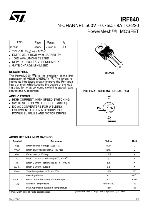
1/8May 2002IRF840N-CHANNEL 500V - 0.75Ω - 8A TO-220PowerMesh™II MOSFETs TYPICAL R DS (on) = 0.75 Ωs EXTREMELY HIGH dv/dt CAPABILITY s 100% AVALANCHE TESTEDs NEW HIGH VOLTAGE BENCHMARK sGATE CHARGE MINIMIZEDDESCRIPTIONThe PowerMESH ™II is the evolution of the first generation of MESH OVERLAY ™. The layout re-finements introduced greatly improve the Ron*area figure of merit while keeping the device at the lead-ing edge for what concerns switching speed, gate charge and ruggedness.APPLICATIONSs HIGH CURRENT, HIGH SPEED SWITCHING s SWITH MODE POWER SUPPLIES (SMPS)s DC-AC CONVERTERS FOR WELDING EQUIPMENT AND UNINTERRUPTIBLE POWER SUPPLIES AND MOTOR DRIVESABSOLUTE MAXIMUM RATINGS(•)Pulse width limited by safe operating areaTYPE V DSS R DS(on)I D IRF840500 V< 0.85 Ω8 ASymbol ParameterValue UnitV DS Drain-source Voltage (V GS = 0)500V V DGR Drain-gate Voltage (R GS = 20 k Ω)500V V GS Gate- source Voltage± 20V I D Drain Current (continuos) at T C = 25°C 8A I D Drain Current (continuos) at T C = 100°C 5.1A I DM (l )Drain Current (pulsed)32A P TOTTotal Dissipation at T C = 25°C 125W Derating Factor1.0W/°C dv/dt (1)Peak Diode Recovery voltage slope 3.5V/ns T stg Storage Temperature–65 to 150°C T jMax. Operating Junction Temperature150°CSD DD (BR)DSS j JMAX.IRF8402/8THERMAL DATAAVALANCHE CHARACTERISTICSELECTRICAL CHARACTERISTICS (TCASE = 25 °C UNLESS OTHERWISE SPECIFIED)OFFON (1)DYNAMICRthj-case Thermal Resistance Junction-case Max 1°C/W Rthj-ambThermal Resistance Junction-ambient Max62.5°C/W T lMaximum Lead Temperature For Soldering Purpose300°CSymbol ParameterMax ValueUnit I AR Avalanche Current, Repetitive or Not-Repetitive (pulse width limited by T j max)8A E ASSingle Pulse Avalanche Energy(starting T j = 25 °C, I D = I AR , V DD = 50 V)520mJSymbol ParameterTest ConditionsMin.Typ.Max.Unit V (BR)DSS Drain-sourceBreakdown Voltage I D = 250 µA, V GS = 0500V I DSS Zero Gate VoltageDrain Current (V GS = 0)V DS = Max Rating1µA V DS = Max Rating, T C = 125 °C 50µA I GSSGate-body Leakage Current (V DS = 0)V GS = ± 20V±100nASymbol ParameterTest ConditionsMin.Typ.Max.Unit V GS(th)Gate Threshold Voltage V DS = V GS , I D = 250µA 234V R DS(on)Static Drain-source On ResistanceV GS = 10V, I D = 3.5 A0.750.85ΩSymbol ParameterTest ConditionsMin.Typ.Max.Unit g fs (1)Forward Transconductance V DS > I D(on) x R DS(on)max, I D =3.5A6.4S C iss Input Capacitance V DS = 25V, f = 1 MHz, V GS = 0832pF C oss Output Capacitance 131pF C rssReverse Transfer Capacitance17pF3/8IRF840ELECTRICAL CHARACTERISTICS (CONTINUED)SWITCHING ONSWITCHING OFFSOURCE DRAIN DIODENote: 1.Pulsed: Pulse duration = 300 µs, duty cycle 1.5 %.2.Pulse width limited by safe operating area.Symbol ParameterTest ConditionsMin.Typ.Max.Unit t d(on)t r Turn-on Delay Time Rise Time V DD = 250 V, I D = 3.5 A R G =4.7Ω V GS = 10 V (see test circuit, Figure 3)1021ns ns Q g Total Gate Charge V DD = 400V, I D = 7 A,V GS = 10V29.639nC Q gs Gate-Source Charge 4.9nC Q gdGate-Drain Charge13.9nCSymbol ParameterTest ConditionsMin.Typ.Max.Unit t r(Voff)Off-voltage Rise TimeV DD = 400V, I D = 7 A, R G =4.7Ω, V GS = 10V (see test circuit, Figure 5)9ns t f Fall Time 9ns t cCross-over Time19nsSymbol ParameterTest ConditionsMin.Typ.Max.Unit I SD Source-drain Current 8A I SDM (2)Source-drain Current (pulsed)32A V SD (1)Forward On Voltage I SD = 8 A, V GS = 0 1.6V t rr Reverse Recovery Time I SD = 7 A, di/dt = 100A/µs V DD = 100V, T j = 150°C (see test circuit, Figure 5)384ns Q rr Reverse Recovery Charge 2.2µC I RRMReverse Recovery Current11.8ASafe Operating Area Thermal ImpedenceIRF8404/8IRF8405/8IRF8406/8Fig. 5: Test Circuit For Inductive Load Switching And Diode Recovery TimesFig. 4: Gate Charge test CircuitFig. 2: Unclamped Inductive WaveformFig. 1:Unclamped Inductive Load Test CircuitFig. 3: Switching Times Test Circuit ForResistive LoadIRF8407/8IRF8408/8Information furnished is believed to be accurate and reliable. However, STMicroelectronics assumes no responsibility for the consequences of use of such information nor for any infringement of patents or other rights of third parties which may result from its use. No license is granted by implication or otherwise under any patent or patent rights of STMicroelectronics. Specifications mentioned in this publication are subject to change without notice. This publication supersedes and replaces all information previously supplied. STMicroelectronics products are not authorized for use as critical components in life support devices or systems without express written approval of STMicroelectronics.© The ST logo is a registered trademark of STMicroelectronics© 2002 STMicroelectronics - Printed in Italy - All Rights ReservedSTMicroelectronics GROUP OF COMPANIESAustralia - Brazil - Canada - China - Finland - France - Germany - Hong Kong - India - Israel - Italy - Japan - Malaysia - Malta - Morocco Singapore - Spain - Sweden - Switzerland - United Kingdom - United States.© 。
常用场效应管型号参数管脚识别及检测表

常用场效应管型号参数管脚识别及检测表场效应管管脚识别场效应管的检测和使用场效应管的检测和使用一、用指针式万用表对场效应管进行判别1用测电阻法判别结型场效应管的电极根据场效应管的PN结正、反向电阻值不一样的现象,可以判别出结型场效应管的三个电极;具体方法:将万用表拨在R×1k档上,任选两个电极,分别测出其正、反向电阻值;当某两个电极的正、反向电阻值相等,且为几千欧姆时,则该两个电极分别是漏极D和源极S;因为对结型场效应管而言,漏极和源极可互换,剩下的电极肯定是栅极G;也可以将万用表的黑表笔红表笔也行任意接触一个电极,另一只表笔依次去接触其余的两个电极,测其电阻值;当出现两次测得的电阻值近似相等时,则黑表笔所接触的电极为栅极,其余两电极分别为漏极和源极;若两次测出的电阻值均很大,说明是PN结的反向,即都是反向电阻,可以判定是N沟道场效应管,且黑表笔接的是栅极;若两次测出的电阻值均很小,说明是正向PN结,即是正向电阻,判定为P沟道场效应管,黑表笔接的也是栅极;若不出现上述情况,可以调换黑、红表笔按上述方法进行测试,直到判别出栅极为止;2用测电阻法判别场效应管的好坏测电阻法是用万用表测量场效应管的源极与漏极、栅极与源极、栅极与漏极、栅极G1与栅极G2之间的电阻值同场效应管手册标明的电阻值是否相符去判别管的好坏;具体方法:首先将万用表置于R×10或R×100档,测量源极S与漏极D之间的电阻,通常在几十欧到几千欧范围在手册中可知,各种不同型号的管,其电阻值是各不相同的,如果测得阻值大于正常值,可能是由于内部接触不良;如果测得阻值是无穷大,可能是内部断极;然后把万用表置于R×10k档,再测栅极G1与G2之间、栅极与源极、栅极与漏极之间的电阻值,当测得其各项电阻值均为无穷大,则说明管是正常的;若测得上述各阻值太小或为通路,则说明管是坏的;要注意,若两个栅极在管内断极,可用元件代换法进行检测;3用感应信号输人法估测场效应管的放大能力具体方法:用万用表电阻的R×100档,红表笔接源极S,黑表笔接漏极D,给场效应管加上1.5V的电源电压,此时表针指示出的漏源极间的电阻值;然后用手捏住结型场效应管的栅极G,将人体的感应电压信号加到栅极上;这样,由于管的放大作用,漏源电压VDS和漏极电流Ib都要发生变化,也就是漏源极间电阻发生了变化,由此可以观察到表针有较大幅度的摆动;如果手捏栅极表针摆动较小,说明管的放大能力较差;表针摆动较大,表明管的放大能力大;若表针不动,说明管是坏的;根据上述方法,我们用万用表的R×100档,测结型场效应管3DJ2F;先将管的G极开路,测得漏源电阻RDS为600Ω,用手捏住G极后,表针向左摆动,指示的电阻RDS为12kΩ,表针摆动的幅度较大,说明该管是好的,并有较大的放大能力;运用这种方法时要说明几点:首先,在测试场效应管用手捏住栅极时,万用表针可能向右摆动电阻值减小,也可能向左摆动电阻值增加;这是由于人体感应的交流电压较高,而不同的场效应管用电阻档测量时的工作点可能不同或者工作在饱和区或者在不饱和区所致,试验表明,多数管的RDS增大,即表针向左摆动;少数管的RDS 减小,使表针向右摆动;但无论表针摆动方向如何,只要表针摆动幅度较大,就说明管有较大的放大能力;第二,此方法对MOS场效应管也适用;但要注意,MOS场效应管的输人电阻高,栅极G允许的感应电压不应过高,所以不要直接用手去捏栅极,必须用于握螺丝刀的绝缘柄,用金属杆去碰触栅极,以防止人体感应电荷直接加到栅极,引起栅极击穿;第三,每次测量完毕,应当G-S极间短路一下;这是因为G-S结电容上会充有少量电荷,建立起VGS电压,造成再进行测量时表针可能不动,只有将G-S极间电荷短路放掉才行;4用测电阻法判别无标志的场效应管首先用测量电阻的方法找出两个有电阻值的管脚,也就是源极S和漏极D,余下两个脚为第一栅极G1和第二栅极G2;把先用两表笔测的源极S与漏极D之间的电阻值记下来,对调表笔再测量一次,把其测得电阻值记下来,两次测得阻值较大的一次,黑表笔所接的电极为漏极D;红表笔所接的为源极S;用这种方法判别出来的S、D极,还可以用估测其管的放大能力的方法进行验证,即放大能力大的黑表笔所接的是D极;红表笔所接地是8极,两种方法检测结果均应一样;当确定了漏极D、源极S的位置后,按D、S的对应位置装人电路,一般G1、G2也会依次对准位置,这就确定了两个栅极G1、G2的位置,从而就确定了D、S、G1、G2管脚的顺序;5用测反向电阻值的变化判断跨导的大小对VMOSN沟道增强型场效应管测量跨导性能时,可用红表笔接源极S、黑表笔接漏极D,这就相当于在源、漏极之间加了一个反向电压;此时栅极是开路的,管的反向电阻值是很不稳定的;将万用表的欧姆档选在R×10kΩ的高阻档,此时表内电压较高;当用手接触栅极G时,会发现管的反向电阻值有明显地变化,其变化越大,说明管的跨导值越高;如果被测管的跨导很小,用此法测时,反向阻值变化不大;二、.场效应管的使用注意事项1为了安全使用场效应管,在线路的设计中不能超过管的耗散功率,最大漏源电压、最大栅源电压和最大电流等参数的极限值;2各类型场效应管在使用时,都要严格按要求的偏置接人电路中,要遵守场效应管偏置的极性;如结型场效应管栅源漏之间是PN结,N沟道管栅极不能加正偏压;P沟道管栅极不能加负偏压,等等; 3MOS场效应管由于输人阻抗极高,所以在运输、贮藏中必须将引出脚短路,要用金属屏蔽包装,以防止外来感应电势将栅极击穿;尤其要注意,不能将MOS场效应管放人塑料盒子内,保存时最好放在金属盒内,同时也要注意管的防潮;4为了防止场效应管栅极感应击穿,要求一切测试仪器、工作台、电烙铁、线路本身都必须有良好的接地;管脚在焊接时,先焊源极;在连入电路之前,管的全部引线端保持互相短接状态,焊接完后才把短接材料去掉;从元器件架上取下管时,应以适当的方式确保人体接地如采用接地环等;当然,如果能采用先进的气热型电烙铁,焊接场效应管是比较方便的,并且确保安全;在未关断电源时,绝对不可以把管插人电路或从电路中拔出;以上安全措施在使用场效应管时必须注意;5在安装场效应管时,注意安装的位置要尽量避免靠近发热元件;为了防管件振动,有必要将管壳体紧固起来;管脚引线在弯曲时,应当大于根部尺寸5毫米处进行,以防止弯断管脚和引起漏气等;对于功率型场效应管,要有良好的散热条件;因为功率型场效应管在高负荷条件下运用,必须设计足够的散热器,确保壳体温度不超过额定值,使器件长期稳定可靠地工作;总之,确保场效应管安全使用,要注意的事项是多种多样,采取的安全措施也是各种各样,广大的专业技术人员,特别是广大的电子爱好者,都要根据自己的实际情况出发,采取切实可行的办法,安全有效地用好场效应管;常用场效应管型号参数表型号参数IRF530NMOS100V14A79W IRFP9530 PMOS100V12A75WIRF540 NMOS100V28A150W IRFP9540 PMOS60V18A100WIRF630 NMOS200V9A75WIRFP9630 PMOS200V6.5A75WIRF640 NMOS200V18A125WIRF720 NMOS400V3.3A50WIRF730 NMOS400V5.5A75WIRF740 NMOS400V10A125WIRF830NMOS500V4.5A75WIRF840NMOS500V8A125W场效应管分类型号耐压电流封装DISCRETE MOS FET 2N7000 60V,0.115A TO-92 DISCRETEMOS FET 2N7002 60V,0.2A SOT-23 DISCRETEMOS FET IRF510A 100V,5.6A TO-220 DISCRETEMOS FET IRF520A 100V,9.2A TO-220 DISCRETEDISCRETEMOS FET IRF540A 100V,28A TO-220 DISCRETEMOS FET IRF610A 200V,3.3A TO-220 DISCRETEMOS FET IRF620A 200V,5A TO-220 DISCRETEMOS FET IRF630A 200V,9A TO-220 DISCRETEMOS FET IRF634A 250V,8.1A TO-220 DISCRETEMOS FET IRF640A 200V,18A TO-220 DISCRETEMOS FET IRF644A 250V,14A TO-220 DISCRETEMOS FET IRF650A 200V,28A TO-220 DISCRETEMOS FET IRF654A 250V,21A TO-220 DISCRETEMOS FET IRF720A 400V,3.3A TO-220 DISCRETEDISCRETEMOS FET IRF740A 400V,10A TO-220 DISCRETEMOS FET IRF750A 400V,15A TO-220 DISCRETEMOS FET IRF820A 500V,2.5A TO-220 DISCRETEMOS FET IRF830A 500V,4.5A TO-220 DISCRETEMOS FET IRF840A 500V,8A TO-220 DISCRETEMOS FET IRF9520 TO-220 DISCRETEMOS FET IRF9540 TO-220 DISCRETEMOS FET IRF9610 TO-220 DISCRETEMOS FET IRF9620 TO-220 DISCRETEMOS FET IRFP150A 100V,43A TO-3P DISCRETEMOS FET IRFP250A 200V,32A TO-3P DISCRETEMOS FET IRFP450A 500V,14A TO-3P DISCRETEMOS FET IRFR024A 60V,15A D-PAK DISCRETEMOS FET IRFR120A 100V,8.4A D-PAK DISCRETEMOS FET IRFR214A 250V,2.2A D-PAK DISCRETEMOS FET IRFR220A 200V,4.6A D-PAK DISCRETEMOS FET IRFR224A 250V,3.8A D-PAK DISCRETEMOS FET IRFR310A 400V,1.7A D-PAK DISCRETEMOS FET IRFR9020TF D-PAK DISCRETEMOS FET IRFS540A 100V,17A TO-220F DISCRETEMOS FET IRFS630A 200V,6.5A TO-220F DISCRETEMOS FET IRFS634A 250V,5.8A TO-220F DISCRETEMOS FET IRFS640A 200V,9.8A TO-220F DISCRETEMOS FET IRFS644A 250V,7.9A TO-220F DISCRETEMOS FET IRFS730A 400V,3.9A TO-220F DISCRETEMOS FET IRFS740A 400V,5.7A TO-220F DISCRETEMOS FET IRFS830A 500V,3.1A TO-220F DISCRETEMOS FET IRFS840A 500V,4.6A TO-220F DISCRETEMOS FET IRFS9Z34 -60V,12A TO-220F DISCRETEMOS FET IRFSZ24A 60V,14A TO-220F DISCRETEMOS FET IRFSZ34A 60V,20A TO-220F DISCRETEMOS FET IRFU110A 100V,4.7A I-PAK DISCRETEMOS FET IRFU120A 100V,8.4A I-PAK DISCRETEMOS FET IRFU220A 200V,4.6A I-PAK DISCRETEMOS FET IRFU230A 200V,7.5A I-PAK DISCRETEMOS FET IRFU410A 500V I-PAK DISCRETEMOS FET IRFU420A 500V,2.3A I-PAK DISCRETEMOS FET IRFZ20A TO-220 DISCRETEMOS FET IRFZ24A 60V,17A TO-220 DISCRETEMOS FET IRFZ30 TO-220 DISCRETEMOS FET IRFZ34A 60V,30A TO-220 DISCRETEMOS FET IRFZ40 TO-220 DISCRETEMOS FET IRFZ44A 60V,50A TO-220 DISCRETEMOS FET IRLS530A 100V,10.7A,Logic TO-220F DISCRETEMOS FET IRLSZ14A 60V,8A,Logic TO-220F DISCRETEMOS FET IRLZ24A 60V,17A,Logic TO-220 DISCRETEMOS FET IRLZ44A 60V,50A,Logic TO-220 DISCRETEMOS FET SFP36N03 30V,36A TO-220 DISCRETEMOS FET SFP65N06 60V,65A TO-220 DISCRETEMOS FET SFP9540 -100V,17A TO-220 DISCRETEMOS FET SFP9634 -250V,5A TO-220 DISCRETEMOS FET SFP9644 -250V,8.6A TO-220 DISCRETEMOS FET SFP9Z34 -60V,18A TO-220 DISCRETEMOS FET SFR9214 -250V,1.53A D-PAK DISCRETEMOS FET SFR9224 -250V,2.5A D-PAK DISCRETEMOS FET SFR9310 -400V,1.5A D-PAK DISCRETEMOS FET SFS9630 -200V,4.4A TO-220F DISCRETEMOS FET SFS9634 -250V,3.4A TO-220F DISCRETEMOS FET SFU9220 -200V,3.1A I-PAK DISCRETEMOS FET SSD2002 25V N/P Dual 8SOP DISCRETEMOS FET SSD2019 20V P-ch Dual 8SOP DISCRETEMOS FET SSD2101 30V N-ch Single 8SOP DISCRETEMOS FET SSH10N80A 800V,10A TO-3P DISCRETEMOS FET SSH10N90A 900V,10A TO-3P DISCRETEMOS FET SSH5N90A 900V,5A TO-3P DISCRETEMOS FET SSH60N10 TO-3P DISCRETEMOS FET SSH6N80A 800V,6A TO-3P DISCRETEMOS FET SSH70N10A 100V,70A TO-3P DISCRETEMOS FET SSH7N90A 900V,7A TO-3P DISCRETEMOS FET SSH9N80A 800V,9A TO-3P DISCRETEMOS FET SSP10N60A 600V,9A TO-220 DISCRETEMOS FET SSP1N60A 600V,1A TO-220 DISCRETEMOS FET SSP2N90A 900V,2A TO-220 DISCRETEMOS FET SSP35N03 30V,35A TO-220 DISCRETEMOS FET SSP3N90A 900V,3A TO-220 DISCRETEMOS FET SSP4N60A 600V,4A TO-220 DISCRETEMOS FET SSP4N60AS 600V,4A TO-220 DISCRETEMOS FET SSP4N90AS 900V,4.5A TO-220 DISCRETEMOS FET SSP5N90A 900V,5A TO-220 DISCRETEMOS FET SSP60N06 60V,60A TO-220 DISCRETEMOS FET SSP6N60A 600V,6A TO-220 DISCRETEMOS FET SSP70N10A 100V,55A TO-220 DISCRETEMOS FET SSP7N60A 600V,7A TO-220 DISCRETEMOS FET SSP7N80A 800V,7A TO-220 DISCRETEMOS FET SSP80N06A 60V,80A TO-220 DISCRETEMOS FET SSR1N60A 600V,0.9A D-PAK DISCRETEMOS FET SSR2N60A 600V,1.8A D-PAK DISCRETEMOS FET SSR3055A 60V,8A D-PAK DISCRETEMOS FET SSS10N60A 600V,5.1A TO-220F DISCRETEMOS FET SSS2N60A 600V,1.3A TO-220F DISCRETEMOS FET SSS3N80A 800V,2A TO-220F DISCRETEMOS FET SSS3N90A 900V,2A TO-220F DISCRETEMOS FET SSS4N60A 600V,3.5A TO-220F/P DISCRETEMOS FET SSS4N60AS 600V,2.3A TO-220F/P DISCRETEMOS FET SSS4N60AS 600V,2.3A TO-220F DISCRETEMOS FET SSS4N90AS 900V,2.8A TO-220F DISCRETEMOS FET SSS5N80A 800V,3A TO-220F DISCRETEMOS FET SSS6N60A 600V, TO-220F/P。
常用场效应管型号参数管脚识别及检测表
常用场效应管型号参数管脚识别及检测表场效应管管脚识别场效应管的检测和使用场效应管的检测和使用一、用指针式万用表对场效应管进行判别(1)用测电阻法判别结型场效应管的电极根据场效应管的PN结正、反向电阻值不一样的现象,可以判别出结型场效应管的三个电极。
具体方法:将万用表拨在R×1k档上,任选两个电极,分别测出其正、反向电阻值。
当某两个电极的正、反向电阻值相等,且为几千欧姆时,则该两个电极分别是漏极D和源极S。
因为对结型场效应管而言,漏极和源极可互换,剩下的电极肯定是栅极G。
也可以将万用表的黑表笔(红表笔也行)任意接触一个电极,另一只表笔依次去接触其余的两个电极,测其电阻值。
当出现两次测得的电阻值近似相等时,则黑表笔所接触的电极为栅极,其余两电极分别为漏极和源极。
若两次测出的电阻值均很大,说明是PN结的反向,即都是反向电阻,可以判定是N沟道场效应管,且黑表笔接的是栅极;若两次测出的电阻值均很小,说明是正向PN结,即是正向电阻,判定为P沟道场效应管,黑表笔接的也是栅极。
若不出现上述情况,可以调换黑、红表笔按上述方法进行测试,直到判别出栅极为止。
(2)用测电阻法判别场效应管的好坏测电阻法是用万用表测量场效应管的源极与漏极、栅极与源极、栅极与漏极、栅极G1与栅极G2之间的电阻值同场效应管手册标明的电阻值是否相符去判别管的好坏。
具体方法:首先将万用表置于R×10或R×100档,测量源极S与漏极D之间的电阻,通常在几十欧到几千欧范围(在手册中可知,各种不同型号的管,其电阻值是各不相同的),如果测得阻值大于正常值,可能是由于内部接触不良;如果测得阻值是无穷大,可能是内部断极。
然后把万用表置于R×10k档,再测栅极G1与G2之间、栅极与源极、栅极与漏极之间的电阻值,当测得其各项电阻值均为无穷大,则说明管是正常的;若测得上述各阻值太小或为通路,则说明管是坏的。
要注意,若两个栅极在管内断极,可用元件代换法进行检测。
常用场效应管型号参数管脚识别及检测表

常用场效应管型号参数管脚识别及检测表公司内部编号:(GOOD-TMMT-MMUT-UUPTY-UUYY-DTTI-常用场效应管型号参数管脚识别及检测表场效应管管脚识别场效应管的检测和使用场效应管的检测和使用一、用指针式万用表对场效应管进行判别(1)用测电阻法判别结型场效应管的电极根据场效应管的PN结正、反向电阻值不一样的现象,可以判别出结型场效应管的三个电极。
具体方法:将万用表拨在R×1k档上,任选两个电极,分别测出其正、反向电阻值。
当某两个电极的正、反向电阻值相等,且为几千欧姆时,则该两个电极分别是漏极D和源极S。
因为对结型场效应管而言,漏极和源极可互换,剩下的电极肯定是栅极G。
也可以将万用表的黑表笔(红表笔也行)任意接触一个电极,另一只表笔依次去接触其余的两个电极,测其电阻值。
当出现两次测得的电阻值近似相等时,则黑表笔所接触的电极为栅极,其余两电极分别为漏极和源极。
若两次测出的电阻值均很大,说明是PN结的反向,即都是反向电阻,可以判定是N沟道场效应管,且黑表笔接的是栅极;若两次测出的电阻值均很小,说明是正向PN结,即是正向电阻,判定为P沟道场效应管,黑表笔接的也是栅极。
若不出现上述情况,可以调换黑、红表笔按上述方法进行测试,直到判别出栅极为止。
(2)用测电阻法判别场效应管的好坏测电阻法是用万用表测量场效应管的源极与漏极、栅极与源极、栅极与漏极、栅极G1与栅极G2之间的电阻值同场效应管手册标明的电阻值是否相符去判别管的好坏。
具体方法:首先将万用表置于R×10或R×100档,测量源极S与漏极D之间的电阻,通常在几十欧到几千欧范围(在手册中可知,各种不同型号的管,其电阻值是各不相同的),如果测得阻值大于正常值,可能是由于内部接触不良;如果测得阻值是无穷大,可能是内部断极。
然后把万用表置于R×10k档,再测栅极G1与G2之间、栅极与源极、栅极与漏极之间的电阻值,当测得其各项电阻值均为无穷大,则说明管是正常的;若测得上述各阻值太小或为通路,则说明管是坏的。
常用场效应管型号参数管脚识别及检测表
常用场效应管型号参数管脚识别及检测表场效应管管脚识别场效应管的检测和使用场效应管的检测和使用一、用指针式万用表对场效应管进行判别(1)用测电阻法判别结型场效应管的电极根据场效应管的PN结正、反向电阻值不一样的现象,可以判别出结型场效应管的三个电极。
具体方法:将万用表拨在R×1k档上,任选两个电极,分别测出其正、反向电阻值。
当某两个电极的正、反向电阻值相等,且为几千欧姆时,则该两个电极分别是漏极D和源极S。
因为对结型场效应管而言,漏极和源极可互换,剩下的电极肯定是栅极G。
也可以将万用表的黑表笔(红表笔也行)任意接触一个电极,另一只表笔依次去接触其余的两个电极,测其电阻值。
当出现两次测得的电阻值近似相等时,则黑表笔所接触的电极为栅极,其余两电极分别为漏极和源极。
若两次测出的电阻值均很大,说明是PN结的反向,即都是反向电阻,可以判定是N沟道场效应管,且黑表笔接的是栅极;若两次测出的电阻值均很小,说明是正向PN结,即是正向电阻,判定为P沟道场效应管,黑表笔接的也是栅极。
若不出现上述情况,可以调换黑、红表笔按上述方法进行测试,直到判别出栅极为止。
(2)用测电阻法判别场效应管的好坏测电阻法是用万用表测量场效应管的源极与漏极、栅极与源极、栅极与漏极、栅极G1与栅极G2之间的电阻值同场效应管手册标明的电阻值是否相符去判别管的好坏。
具体方法:首先将万用表置于R×10或R×100档,测量源极S与漏极D之间的电阻,通常在几十欧到几千欧范围(在手册中可知,各种不同型号的管,其电阻值是各不相同的),如果测得阻值大于正常值,可能是由于内部接触不良;如果测得阻值是无穷大,可能是内部断极。
然后把万用表置于R×10k档,再测栅极G1与G2之间、栅极与源极、栅极与漏极之间的电阻值,当测得其各项电阻值均为无穷大,则说明管是正常的;若测得上述各阻值太小或为通路,则说明管是坏的。
要注意,若两个栅极在管内断极,可用元件代换法进行检测。
常用场效应管(25N120等)参数及代换
常用场效应管(25N120等)参数及代换FGA25N120AND (IGBT) 1200V/25A//TO3P (电磁炉用)FQA27N25 (MOSFET) 250V/27A/TO3P IRFP254FQA40N25 (MOSFET) 250V/40A/280W/0.051Ω/TO3P IRFP264FQA55N25 (MOSFET) 250V/55A/310W/0.03Ω/TO3PFQA18N50V2 (MOSFET) 500V/20A/277W/0.225Ω IRFP460AFQA24N50 (MOSFET) 500V/24A/290W/0.2Ω/TO3PFQA28N50 (MOSFET) 500V/28.4A/310W/0.126Ω/TO3P MTY30N50EFQL40N50 (MOSFET) 500V/40A/560W/0.085Ω/TO264 IRFPS37N50FQA24N60 (MOSFET) 600V/24A/TO3PFQA10N80 (MOSFET) 800V/9.8A/240W/0.81Ω/TO3PFQA13N80 (MOSFET) 800V/13A/300W/0. Ω/TO3PFQA5N90 (MOSFET) 900V/5.8A/185W/2.3Ω/TO3PFQA9N90C (MOSFET) 900V/8.6A/240W/1.3Ω/TO3PFQA11N90C (MOSFET) 900V/11.4A/300W/0.75Ω/TO3PFFA30U20DN (快恢复二极管) 200V/2×30A/40ns/TO3P DSEK60-02A FFPF30U60S (快恢复二极管) 600V/30A/90ns/TO220F MUR1560FFA30U60DN (快恢复二极管) 600V/2×30A/90ns/TO3P DSEK60-06A MBRP3010NTU (肖特基) 100V/30A/TO-220MBRA3045NTU (肖特基) 45V/30A/TO-3PISL9R3060G2 (快恢复二极管) 600V/30A/35ns/200W/TO247 APT30D60B RHRG3060 (快恢复二极管) 600V/30A/35nS/TO247FQP44N10 (MOSFET) 100V/44A/146W/0.0396Ω/TO220 IRF3710/IRF540N FQP70N10 (MOSFET) 100V/57A/160W/0.025Ω/TO220IRFP450B (MOSFET) 500V/14A/0.4Ω/205W/TO3PIRFP460C (MOSFET) 500V/20A/0.2~0.24Ω/235W IRFP460KA3162/FAN8800 (Drive IC)单IGBT/MOSFETFET驱动ICRHRP860 (快恢复二极管) 600V/8A/30NS/TO-220 MUR860RHRP1560 (快恢复二极管) 600V/15A/TO0220 MUR1560RHRP8120 (快恢复二极管) 1200V/8A/75W/TO220RHRP15120 (快恢复二极管) 1200V/15A/TO220RHRP30120 (快恢复二极管) 1200V/30A/125W/TO220单 DSEI20-10ARHRG30120 (快恢复二极管) 1200V/30A/T03PSSH45N20B (MOSFET) 200V/45A/TO3P IRFP260FGL40N150D (IGBT) 1500V/40A/TO264快速IGBTFGL60N100BNTD (IGBT) 1000V/60A/TO264快速IGBT 1MBH60-100HGTG10N120BND (IGBT) 1200V/35A/298W/100ns/TO247HGTG11N120CND (IGBT) 1200V/43A/298W/TO247HGTG18N120BND (IGBT) 1200V/54A/390W/90ns/TO247FQP5N50C (MOSFET) 500V/5A/73W/1.4Ω/TO-220 替代:IRF830,用于35W FQPF5N50C (MOSFET) 500V/5A/38W/1.4Ω/TO-220F 替代:IRF830,用于35W FQP9N50C (MOSFET) 500V/9A/135W/0.6Ω/TO220 替代:IRF840,用于75W FQPF9N50C (MOSFET) 500V/9A/44W/0.6Ω/TO-220F 替代:IRF840,用于75W FQP13N50 (MOSFET) 500V/13.4A/190W/0.43Ω/TO220 用于75W/125W产品FQPF13N50 (MOSFET) 500V/13.4A/48W/0.43Ω/TO220F 用于75W/125W产品FQD5N50C (MOSFET) 500V/5A/1.4Ω/TO252 用于35WFQA16N50 (MOSFET) 500V/16A/200W/0.32C/TO3P 用于150W到250W的产品FDP15N50 (MOSFET) 500V/15A/0.43Ω/56W/TO220 用于150W左右的产品FQP18N50V2 (MOSFET) 500V/18A/0.43Ω/208W/TO220 用于250WG到400W的产品FQPF18N50V2 (MOSFET) 500V/18A/0.43Ω/56W/TO220 用于250WG到400W的产品FQA18N50V2 (MOSFET) 500V/20A/277W/0.225Ω/TO3P 用于250WG到400W的产品FQA24N50 (MOSFET) 500V/24A/290W/0.2Ω/TO3P 用于400W的产品FQA24N60 (MOSFET) 600V/23.5A/310W/0.24Ω/TO3P 用于400W的产品FQA28N50 (MOSFET) 500V/28.4A/310W/0.126Ω/TO3P 用于400W的产品FQL40N50 (MOSFET) 500V/40A/560W/0.085Ω/TO264 用于560W的产品IRF740B (MOSFET) 400V/10A/0.55Ω/134W/TO220IRF730B (MOSFET) 400V/5.5A/1.0Ω/73W/TO220IRF830B (MOSFET) 500V/4.5A/1.5Ω/73W/TO220 IRF840B (MOSFET) 500V/8A/0.85Ω/134W/TO220 IRFP450B (MOSFET) 500V/14A/0.4Ω/205W/TO3P IRFP460C (MOSFET) 500V/20A/0.2~0.24Ω/235W FQPF5N60C (MOSFET) 600V/5A/TO220FFQPF8N60C (MOSFET) 600V/8A/TO220FFQPF10N60C (MOSFET) 600V/10A/TO220FQPF12N60 (MOSFET) 600V/12A/51W/0.65Ω/TO220F FCP11N60 (MOSFET) 650V/11A/125W0.32Ω/TO220 RHRD660S (快恢复二极管) 600V/6A/TO-252RHRP860 (快恢复二极管) 600V/8A/75W/TO-220 RHRP1560 (快恢复二极管) 600V/15A/TO-220单2N7002 (三极管) 60V/0.12A/SOT-23HUF76629D3S (MOSFET) 100V/20A/110W/TO-252 HUF75639S3S (MOSFET) 100V/56A/200W/TO-263ISL9V3040D3S (IGBT) 430V/21A/150W/300MJ/TO252 ISL9V3040S3S (IGBT) 430V/21A/150W/300MJ/TO263 ISL9V5036S3S (IGBT) 360V/46A/250W/TO262FQP33N10L (MOSFET) 100V/33A/52MΩ127W/TO220。
irf840场效应管参数
irf840场效应管参数
irf840场效应管是一种N型场效应管,它的特性参数如下:
1.最大电压:VDSS=200V,即场效应管的最大漏源极电压为200V;
2.最大电流:ID=8A,即场效应管的最大漏源极电流为8A;
3.最小漏源极间电阻:RDS(on)=0.0085Ω,即场效应管的最小漏源极间电阻为0.0085Ω;
4.最大功耗:PD=25W,即场效应管的最大功耗为25W;
5.最大漏源极电容:Ciss=1000pF,即场效应管的最大漏源极电容为1000pF;
6.最大漏极极电容:Coss=50pF,即场效应管的最大漏极极电容为50pF;
7.最大漏极极电容:Crss=10pF,即场效应管的最大漏极极电容为10pF;
8.最大增益带宽:ft=100MHz,即场效应管的最大增益带宽为100MHz;
9.最大增益:hFE=50,即场效应管的最大增益为50。
irf840场效应管的特性参数可以满足大多数电子设备的要求,因此在电子设备中应用比较广泛。
它的最大电压、最大电流、最小漏源极间电阻、最大功耗、最大漏源极电容、最大漏极极电容、最大增益带宽和最大增益等参数都是比较重要的,可以根据不同的应用场合来选择合适的参数。
常用场效应管型号参数管脚识别及检测表
经常使用场效应管型号参数管脚识别及检测表之阿布丰王创作场效应管管脚识别场效应管的检测和使用场效应管的检测和使用一、用指针式万用表对场效应管进行判别(1)用测电阻法判别结型场效应管的电极根据场效应管的PN结正、反向电阻值纷歧样的现象,可以判别出结型场效应管的三个电极。
具体方法:将万用表拨在R×1k档上,任选两个电极,分别测出其正、反向电阻值。
当某两个电极的正、反向电阻值相等,且为几千欧姆时,则该两个电极分别是漏极D和源极S。
因为对结型场效应管而言,漏极和源极可互换,剩下的电极肯定是栅极G。
也可以将万用表的黑表笔(红表笔也行)任意接触一个电极,另一只表笔依次去接触其余的两个电极,测其电阻值。
当出现两次测得的电阻值近似相等时,则黑表笔所接触的电极为栅极,其余两电极分别为漏极和源极。
若两次测出的电阻值均很大,说明是PN结的反向,即都是反向电阻,可以判定是N沟道场效应管,且黑表笔接的是栅极;若两次测出的电阻值均很小,说明是正向PN结,即是正向电阻,判定为P沟道场效应管,黑表笔接的也是栅极。
若不出现上述情况,可以调换黑、红表笔按上述方法进行测试,直到判别出栅极为止。
(2)用测电阻法判别场效应管的好坏测电阻法是用万用表丈量场效应管的源极与漏极、栅极与源极、栅极与漏极、栅极G1与栅极G2之间的电阻值同场效应管手册标明的电阻值是否相符去判别管的好坏。
具体方法:首先将万用表置于R×10或R×100档,丈量源极S与漏极D之间的电阻,通常在几十欧到几千欧范围(在手册中可知,各种分歧型号的管,其电阻值是各不相同的),如果测得阻值大于正常值,可能是由于内部接触不良;如果测得阻值是无穷大,可能是内部断极。
然后把万用表置于R×10k档,再测栅极G1与G2之间、栅极与源极、栅极与漏极之间的电阻值,当测得其各项电阻值均为无穷大,则说明管是正常的;若测得上述各阻值太小或为通路,则说明管是坏的。
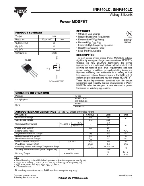
IRF840LC中文资料
Power MOSFETIRF840LC, SiHF840LCVishay SiliconixFEATURES•Ultra Low Gate Charge•Reduced Gate Drive Requirement •Enhanced 30 V V GS Rating •Reduced C iss , C oss , C rss•Extremely High Frequency Operation •Repetitive Avalanche Rated •Lead (Pb)-free AvailableDESCRIPTIONThis new series of low charge Power MOSFETs achieve signiticantly lower gate charge over conventional MOSFETs.Utilizing the new LCDMOS technology, the device improvements are achieved without added product cost,allowing for reduced gate drive requirements and total system savings. In addition, reduced switching losses and improved efficiency are achievable in a variety of high frequency applications. Frequencies of a few MH z at high current are possible using the new low charge MOSFETs.These device improvements combined with the proven ruggedness and reliability that are characteristic of Power MOSFETs offer the designer a new standard in power transistors for switching applications.Notesa.Repetitive rating; pulse width limited by maximum junction temperature (see fig. 11).b.V DD = 50 V, starting T J = 25 °C, L = 14 mH, R G = 25 Ω, I AS = 8.0 A (see fig. 12).c.I SD ≤ 8.0 A, dI/dt ≤ 100 A/µs, V DD ≤ V DS , T J ≤ 150 °C.d. 1.6 mm from case.PRODUCT SUMMARYV DS (V)500R DS(on) (Ω)V GS = 10 V0.85Q g (Max.) (nC)39Q gs (nC)10Q gd (nC)19ConfigurationSingleTO-220GDSORDERING INFORMATIONPackage TO-220Lead (Pb)-free IRF840LCPbF SiHF840LC-E3SnPbIRF840LC SiHF840LCABSOLUTE MAXIMUM RATINGS T C = 25 °C, unless otherwise notedARAMETER SYMBOL LIMIT UNIT Drain-Source Voltage V DS 500V Gate-Source Voltage V GS ±30Continuous Drain Current V GS at 10 V T C = 25 °C I D8.0AT C = 100 °C5.1Pulsed Drain Currenta I DM 28Linear Derating Factor 1.0W/°C Single Pulse Avalanche Energy b E AS 510mJ Repetitive Avalanche Current a I AR 8.0 A Repetitive Avalanche Energya E AR 13mJ Maximum Power Dissipation T C = 25 °CP D 125WPeak Diode Recovery dV/dtc dV/dt 3.5V/ns Operating Junction and Storage Temperature Range T J , T stg- 55 to + 150 °C Soldering Recommendations (Peak Temperature)for 10 s 300dMounting Torque 6-32 or M3 screw10lbf · in 1.1N · m* Pb containing terminations are not RoHS compliant, exemptions may applyIRF840LC, SiHF840LCVishay SiliconixNotesa.Repetitive rating; pulse width limited by maximum junction temperature (see fig. 11).b.Pulse width ≤ 300 µs; duty cycle ≤ 2 %.THERMAL RESISTANCEARAMETER SYMBOL TY.MAX.UNITMaximum Junction-to-Ambient R thJA -62°C/W Case-to-Sink, Flat, Greased Surface R thCS 0.50-Maximum Junction-to-Case (Drain)R thJC- 1.0IRF840LC, SiHF840LCVishay SiliconixIRF840LC, SiHF840LCVishay SiliconixFig. 12a - Unclamped Inductive Test Circuit Fig. 12b - Unclamped Inductive WaveformsIRF840LC, SiHF840LCVishay SiliconixFig. 13a - Basic Gate Charge WaveformFig. 13b - Gate Charge Test CircuitIRF840LC, SiHF840LCVishay Siliconix Array Fig. 14 - For N-ChannelVishay Siliconix maintains worldwide manufacturing capability. Products may be manufactured at one of several qualified locations. Reliability data for Silicon Technology and Package Reliability represent a composite of all qualified locations. For related documents such as package/tape drawings, part marking, andreliability data, see /ppg?91067.Disclaimer Legal Disclaimer NoticeVishayAll product specifications and data are subject to change without notice.Vishay Intertechnology, Inc., its affiliates, agents, and employees, and all persons acting on its or their behalf (collectively, “Vishay”), disclaim any and all liability for any errors, inaccuracies or incompleteness contained herein or in any other disclosure relating to any product.Vishay disclaims any and all liability arising out of the use or application of any product described herein or of any information provided herein to the maximum extent permitted by law. The product specifications do not expand or otherwise modify Vishay’s terms and conditions of purchase, including but not limited to the warranty expressed therein, which apply to these products.No license, express or implied, by estoppel or otherwise, to any intellectual property rights is granted by this document or by any conduct of Vishay.The products shown herein are not designed for use in medical, life-saving, or life-sustaining applications unless otherwise expressly indicated. Customers using or selling Vishay products not expressly indicated for use in such applications do so entirely at their own risk and agree to fully indemnify Vishay for any damages arising or resulting from such use or sale. Please contact authorized Vishay personnel to obtain written terms and conditions regarding products designed for such applications.Product names and markings noted herein may be trademarks of their respective owners.元器件交易网。
IRF840AL规格书
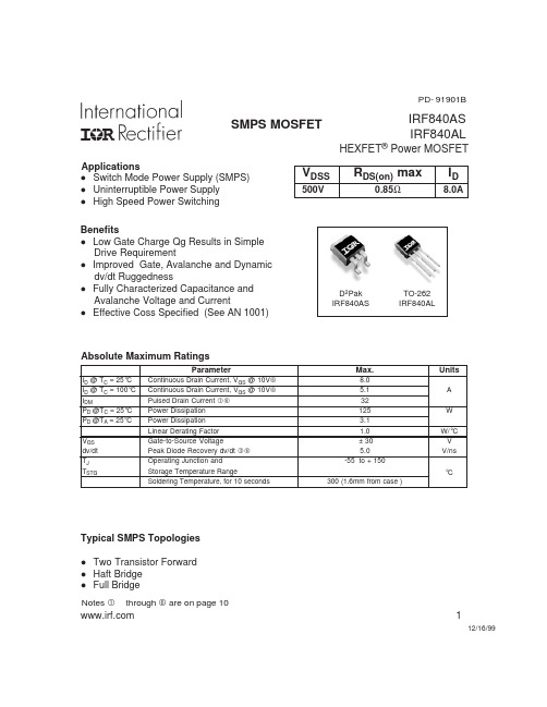
Min. Typ. Max. Units
Conditions D MOSFET symbol ––– ––– 8.0 showing the A G integral reverse ––– ––– 32 S p-n junction diode. ––– ––– 2.0 V TJ = 25°C, IS = 8.0A, VGS = 0V ––– 422 633 ns TJ = 25°C, IF = 8.0A ––– 2.0 3.0 µC di/dt = 100A/µs Intrinsic turn-on time is negligible (turn-on is dominated by LS+LD)
TJ , Junction Temperature ( °C)
Fig 3. Typical Transfer Characteristics
Fig 4. Normalized On-Resistance Vs. Temperature
3
IRF840AS/L
100000
20
VGS , Gate-to-Source Voltage (V)
Min. 500 ––– ––– 2.0 ––– ––– ––– ––– Min. 3.7 ––– ––– ––– ––– ––– ––– ––– ––– ––– ––– ––– ––– –––
Typ. ––– 0.58 ––– ––– ––– ––– ––– ––– Typ. ––– ––– ––– ––– 11 23 26 19 1018 155 8.0 1490 42 56
Max.
8.0 5.1 32 125 3.1 1.0 ± 30 5.0 -55 to + 150 300 (1.6mm from case )
IRFS840A中文资料

Value Units A V mJ A mJ V/ns W W/A V TO-220F1.Gate2. Drain3. Source321oC5004.62.9326474.64.43.5440.3530TRADEMARKSACEx™CoolFET™CROSSVOLT™E 2CMOS TM FACT™FACT Quiet Series™FAST ®FASTr™GTO™HiSeC™The following are registered and unregistered trademarks Fairchild Semiconductor owns or is authorized to use and is not intended to be an exhaustive list of all such trademarks.LIFE SUPPORT POLICYFAIRCHILD’S PRODUCTS ARE NOT AUTHORIZED FOR USE AS CRITICAL COMPONENTS IN LIFE SUPPORTDEVICES OR SYSTEMS WITHOUT THE EXPRESS WRITTEN APPROV AL OF FAIRCHILD SEMICONDUCTOR CORPORA TION.As used herein:ISOPLANAR™MICROWIRE™POP™PowerTrench™QS™Quiet Series™SuperSOT™-3SuperSOT™-6SuperSOT™-8TinyLogic™1. Life support devices or systems are devices or systems which, (a) are intended for surgical implant intothe body, or (b) support or sustain life, or (c) whosefailure to perform when properly used in accordancewith instructions for use provided in the labeling, can be reasonably expected to result in significant injury to the user.2. A critical component is any component of a lifesupport device or system whose failure to perform can be reasonably expected to cause the failure of the life support device or system, or to affect its safety or effectiveness.PRODUCT STATUS DEFINITIONS Definition of Terms Datasheet Identification Product Status DefinitionAdvance InformationPreliminary No Identification Needed Obsolete This datasheet contains the design specifications for product development. Specifications may change in any manner without notice.This datasheet contains preliminary data, andsupplementary data will be published at a later date.Fairchild Semiconductor reserves the right to make changes at any time without notice in order to improve design.This datasheet contains final specifications. Fairchild Semiconductor reserves the right to make changes at any time without notice in order to improve design.This datasheet contains specifications on a product that has been discontinued by Fairchild semiconductor.The datasheet is printed for reference information only.Formative or In DesignFirst ProductionFull ProductionNot In ProductionDISCLAIMERFAIRCHILD SEMICONDUCTOR RESERVES THE RIGHT TO MAKE CHANGES WITHOUT FURTHER NOTICE TO ANY PRODUCTS HEREIN TO IMPROVE RELIABILITY , FUNCTION OR DESIGN. FAIRCHILD DOES NOT ASSUME ANY LIABILITY ARISING OUT OF THE APPLICATION OR USE OF ANY PRODUCT OR CIRCUIT DESCRIBED HEREIN; NEITHER DOES IT CONVEY ANY LICENSE UNDER ITS PATENT RIGHTS, NOR THE RIGHTS OF OTHERS.UHC™VCX™。
IRF840中文特性
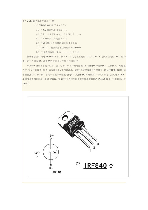
1)V DS :最大工作电压500v
.2)V DG(20KΩ)耐压500V。
3)V GS 栅源电压正负20V
4)ID25度时8A,1OO度时5.1A
5)IDM最大工作电流32A
6)Ptot 温度25度时峰值功率125W
7)Dv/Dt 二极管恢复电压峰值斜率3.5v/ns
8)工作温度范围-65----150度
要使增强型N沟道MOSFET工作,要在G、S之间加正电压VGS及在D、S之间加正电压VDS,则产生正向工作电流ID。
改变VGS的电压可控制工作电流ID
MOSFET全称功率场效应晶体管。
它的三个极分别是源极(S)、漏极(D)和栅极(G)。
主要优点:热稳定性好、安全工作区大。
缺点:击穿电压低,工作电流小。
IGBT全称绝缘栅双极晶体管,是MOSFET和GTR(功率晶管)相结合的产物。
它的三个极分别是集电极(C)、发射极(E)和栅极(G)。
特点:击穿电压可达1200V,集电极最大饱和电流已超过1500A。
由IGBT作为逆变器件的变频器的容量达250kVA以上,工作频率可达20kHz。
SRH840A 用户手册说明书
SRH840AUser's GuideThe Shure professional studio headphones, SRH840A, user guide. Version: 3.4 (2022-C)Table of ContentsSRH840A User's Guide3 Professional Reference Headphones 3 General Description 3 Care and Maintenance3 Cable Lock3 Storage3 Specifications4Accessories5 Furnished Accessories 5 Replacement Parts 5 SAFETY PRECAUTIONS5 CAUTION 5 WARNING 6 WARNING 6 LIMITED WARRANTY6 Service Centers 7 Certifications7••••••••SRH840A User's GuideProfessional Reference HeadphonesGeneral DescriptionThe new SRH840A Professional Studio Headphones are ideal for recording, content creation and monitoring. A precisely tailored frequency response and 40mm neodymium dynamic drivers deliver rich bass, clear mid-range and extended highs. A lightweight, padded headband combined with Shure durability provide the ultimate listening experience.Precisely tailored frequency response delivers rich bass, clear mid-range and extended highsLow distortion 40mm dynamic neodymium drivers offer natural and well-balanced frequency response Comfortable, lightweight headband provides superior comfort for extended useClosed-back, circumaural design rests comfortably over the ears and reduces background noise Folds flat for easy portability and storageSleek, durable design looks great on camera and withstands the rigors of constant use Detachable locking cable securely locks cable into ear cup and enables easy replacementIncludes detachable straight cable, carrying bag, threaded ¼” (6.3 mm) goldplated adapter and 2year warrantyCare and MaintenanceTo clean the headphones, use a soft, damp cloth.CAUTION: Do not use cleansers that contain solvents. Keep liquid and foreign objects out of the driver openings.Cable LockStorageSpecificationsTransducer TypeDynamic, Neodymium magnetDriver Size40 mmFrequency Response5 to 25,000 HzSensitivity@ 1 kHz97 dB/mWImpedance@ 1 kHz40 ΩMaximum Input Power500 mWWeight273 g (9.63 oz.)••ConnectorGoldplated 1/8” (3.5 mm) stereo plug with threaded 1/4” (6.3 mm) goldplated adapterCable3 m (9.84 ft) / detachable, straight, oxygenfree copperAccessoriesFurnished AccessoriesCarrying Pouch for Professional Headphones HPACP13.5mm Bayonet Headphone Audio CableSRH-CABLEReplacement PartsReplacement Ear Cushions for SRH840ASRH840A-PADS Universal 3.5mm Bayonet Headphone Communication Cable RMCH1-UNIReplacement Coil Cable Assembly for SRH HeadphonesSRH-CABLE-COILEDSAFETY PRECAUTIONSThe possible results of incorrect use are marked by one of the two symbols—"WARNING" and "CAUTION"—depending on theimminence of the danger and the severity of the damage.WARNING: Ignoring these warnings may cause severe injury or death as a result of incorrect operation.CAUTION: Ignoring these cautions may cause moderate injury or property damage as a result of incorrect operation.CAUTIONNever disassemble or modify the device, as failures may result.Do not subject to extreme force and do not pull on the cable or failures may result.•••Keep the product dry and avoid exposure to extreme temperatures and humidity.WARNINGIf water or other foreign objects enter the inside of the device, fire or electric shock may result.Do not attempt to modify this product. Doing so could result in personal injury and/or product failure.This device is able to produce sound volume higher than 85 dB SPL. Please check your maximum allowed continuous noise exposure level based on your national employment protection requirements.WARNINGLISTENING TO AUDIO AT EXCESSIVE VOLUMES CAN CAUSE PERMANENT HEARING DAMAGE. USE AS LOW A VOLUME AS POSSIBLE. Over exposure to excessive sound levels can damage your ears resulting in permanent noise-induced hearing loss (NIHL). Please use the following guidelines established by the Occupational Safety Health Administration (OSHA) on maximum time exposure to sound pressure levels before hearing damage occurs.90 dB SPL at 8 hours 95 dB SPLat 4 hours100 dB SPLat 2 hours105 dB SPLat 1 hour110 dB SPL at ½ hour 115 dB SPLat 15 minutes120 dB SPLAvoid or damage may occurLIMITED WARRANTYShure Incorporated (“Shure”) hereby warrants to the original consumer purchaser only that, except as otherwise specified below, this product will be free in normal use of any defects in materials and workmanship for a period of two (2) years from the consumer’s original date of purchase directly from Shure or from a Shureauthorized reseller.Any rechargeable batteries contained in or packaged with this product are so warranted for a period of one (1) year from the consumer’s original date of purchase. However, rechargeable batteries are consumable and their capacity will be reduced over time based on temperature, amount of time in storage, charging cycles, and other factors; hence reduction in battery capacity does not constitute a defect in material or workmanship.At its sole option, Shure will repair or replace the defective product and promptly return it to you. In order for this warranty to be valid, the consumer must, at the time the product is returned, provide proof of purchase in the form of the original purchase receipt directly from Shure or from a Shureauthorized reseller. If Shure elects to replace the defective product, then Shure reserves the right to replace the defective product with another product of the same model or a model of at least comparable quality and features in Shure’s sole determination.If you believe this product is defective within the warranty period, carefully repack the unit, insure it and return it with proof of purchase, postage prepaid, to Shure Incorporated, Attention: Service Department, at the address below.Outside of the United States, return the product to your dealer or Authorized Service Center. Addresses are listed on or can be obtained by contacting Shure at the address listed below.This warranty is not transferable. This warranty does not apply in cases of abuse or misuse of the product, use contrary to Shure’s instruction, ordinary wear and tear, an act of God, negligent use, purchase from a party other than Shure or a Shureauthorized reseller, unauthorized repair, or modification of the product.ALL IMPLIED WARRANTIES OF MERCHANTABILITY OR FITNESS FOR A PARTICULAR PURPOSE ARE HEREBY DISCLAIMED TO THE EXTENT PERMITTED UNDER APPLICABLE LAWS AND, TO THE EXTENT NOT PERMITTED, AREHEREBY LIMITED TO THE DURATION AND TERMS OF THIS WARRANTY. SHURE ALSO HEREBY DISCLAIMS ALL LIABILITY FOR INCIDENTAL, SPECIAL, OR CONSEQUENTIAL DAMAGES.Some states do not allow limitations on how long an implied warranty lasts, or the exclusion or limitation of incidental or consequential damages, so the above limitation may not apply to you. This warranty gives you specific legal rights, and you may have other rights which vary from state to state.This warranty does not restrict the rights of the consumer mandated under applicable laws.THIS WARRANTY SUPERSEDES ALL OTHER WARRANTIES THAT ARE ASSOCIATED OR INCLUDED WITH THIS PRODUCT, EXCEPT THAT ANY SOFTWARE CONTAINED IN OR PACKAGED WITH THIS PRODUCT IS EXCLUDED FROM THIS WARRANTY AND INSTEAD SHALL BE COVERED BY THE WARRANTY, IF ANY, PROVIDED IN SHURE’S END USER LICENSE AGREEMENT ACCOMPANYING SUCH SOFTWARE.Service CentersUnited States, Canada, Latin America, CaribbeanShure IncorporatedAttn: Service Department945 Chaddick Dr.Wheeling, IL 60090-6449 U.S.A.Europe, Middle East, and AfricaShure Europe GmbHAttn: ServiceJakob-Dieffenbacher-Str. 12,75031 Eppingen, GermanyIndonesiaService Center Resmi:Jakarta Hotline (021) 612 6388Medan (061) 6612550Surabaya (031) 5032219Jogjakarta (0274) 371710Denpasar (0361) 766788Makasar (0411) 324652CertificationsThis product meets the Essential Requirements of all relevant European directives and is eligible for CE marking.The CE Declaration of Conformity can be obtained from: /europe/complianceAuthorized European representative:Shure Europe GmbHGlobal ComplianceJakob-Dieffenbacher-Str. 1275031 Eppingen, GermanyPhone: +49-7262-92 49 0Email:*************。
JM840A AC Current Probe用户手册说明书
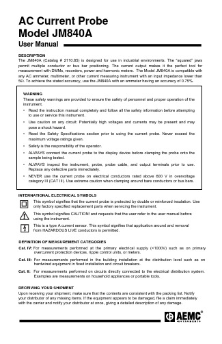
®AC Current Probe Model JM840AUser ManualDESCRIPTIONThe JM840A (Catalog # 2110.85) is designed for use in industrial environments. The “squared” jaws permit multiple conductor or bus bar positioning. The current output makes it the perfect tool for measurement with DMMs, recorders, power and harmonic meters. The Model JM840A is compatible with any AC ammeter, multimeter, or other current measuring instrument with an input impedance lower than 5 . To achieve the stated accuracy, use the JM840A with an ammeter having an accuracy of 0.75%. WARNINGThese safety warnings are provided to ensure the safety of personnel and proper operation of the instrument.•Read the instruction manual completely and follow all the safety information before attempting to use or service this instrument. •Use caution on any circuit: Potentially high voltages and currents may be present and may pose a shock hazard. •Read the Safety Specifications section prior to using the current probe. Never exceed the maximum voltage ratings given. • Safety is the responsibility of the operator.•ALWAYS connect the current probe to the display device before clamping the probe onto the sample being tested. •ALWAYS inspect the instrument, probe, probe cable, and output terminals prior to use.Replace any defective parts immediately.•NEVER use the current probe on electrical conductors rated above 600 V in overvoltage category III (CAT III). Use extreme caution when clamping around bare conductors or bus bars. INTERNATIONAL ELECTRICAL SYMBOLSThis symbol signifies that the current probe is protected by double or reinforced insulation. Use only factory specified replacement parts when servicing the instrument.This symbol signifies CAUTION! and requests that the user refer to the user manual before using the instrument.This is a type A current sensor. This symbol signifies that application around and removal from HAZARDOUS LIVE conductors is permitted.DEFINITION OF MEASUREMENT CATEGORIESCat. I V : For measurements performed at the primary electrical supply (<1000V) such as on primaryovercurrent protection devices, ripple control units, or meters. Cat. II: For measurements performed on circuits directly connected to the electrical distribution system.Examples are measurements on household appliances or portable tools. Cat. III: For measurements performed in the building installation at the distribution level such as onhardwired equipment in fixed installation and circuit breakers. RECEIVING YOUR SHIPMENTUpon receiving your shipment, make sure that the contents are consistent with the packing list. Notify your distributor of any missing items. If the equipment appears to be damaged, file a claim immediately with the carrier and notify your distributor at once, giving a detailed description of any damage.ELECTRICAL SPECIFICATIONS Current Range:1 to 500A AC continuous cycle1 to 1000A AC continuous cycle1 to 1500A AC continuous cycle Transformation Ratio:500:1, 1000:1, 1500:1Output Signal:2mA AC/A AC (1A at 500A)1mA AC/A AC (1A at 1000A)0.66mA AC/A AC (1A at 1500A) Accuracy and Phase Shift*:500A RANGEPrimary current 25A 100A 500A Accuracy % 4% 3% 3% Phase shift 4° 3.5° 2°Load Impedance: 5ΩOverload: 700A for 10 mnAmpere Second Product: 6 A.sAccuracy: Per IEC 185-26-275 VA Class 3 from 48 to 1000 Hz1000A RANGEPrimary current 50A 200A 1000A Accuracy % 3% 2% 1% Phase shift 3° 1.5° 1°Load Impedance: 5ΩOverload: 1400A for 10 mnAmpere Second Product: 30 A.sAccuracy: Per IEC 185-26-275 VA Class 1 from 48 to 1000 Hz1500A RANGEPrimary current 75A 300A 1500A Accuracy % 1.5% 0.75% 0.5% Phase shift 1.5° 0.75° 0.5°Load Impedance: 5ΩOverload: 1800A for 10 mnAmpere Second Product: 65 A.sAccuracy: Per IEC 185-26-275 VA Class 0.5 from 48 to 1000 Hz(*Reference conditions: 23°C±3°K, 20 to 85% RH, 45 to 65 Hz, external magnetic field < 40 A/m, no DC component, no external current carrying conductor, test sample centered.) Frequency Range: 30 to 1500Hz; current derating above 1500Hz for continuous useWorking Voltage: 600V ACCommon Mode Voltage: 600V ACOpen Secondary Voltage: 42V Max.Influence of Adjacent Conductor:< 0.005A/A ACInfluence of Conductor in Jaw Opening: 1.5% ± 0.2A on 500:1 range1% ± 0.2A on 1000:1 range1% ± 0.2A on 1500:1 rangeMECHANICAL SPECIFICATIONS Operating Temp.: 14° to 122°F (-10° to 50°C) Storage Temp.: -13° to 176°F (-25° to 80°C) Influence of Temperature: < 0.1% per 10°K Jaw Opening: 3.54" (90 mm) Maximum Conductor Size:Cable: 2.52" ∅ max. (64mm)Bus bar: 1.97 x 5.31" (50 x 135 mm)2.52 x3.94" (64 x 100 mm)Envelope Protection: IP 20 (IEC 529)Drop Test: 1 m (IEC 68-2-32)Mechanical Shock: 100 g (IEC 68-2-27) Vibration: 10/55/10 Hz, 0.15 mm (IEC 68-2-6) Polycarbonate Material:Handles:10% fiberglass chargedpolycarbonate UL 94 V0Jaws: ABS UL 94 V2Dimensions:4.72 x 12.40 x 1.89" (120 x 315 x 48 mm) Weight: 2.65 lbs. (1200 g)Colors: Dark gray handles with red jaws Output:Two standard safety banana jacks (4mm) SAFETY SPECIFICATIONSElectrical:Double insulation or reinforced insulation between primary or secondary and outer case of handle upon IEC 1010-2-32Common Mode Voltage:600V CAT III, Pollution: 2ORDERING INFORMATIONCurrent Probe JM840A ................... C at #2110.85 Accessories:Leads, set of 2, 5 ft. safety (1000V) .. C at #2111.29 Lead No. 211 for Probe 5A Series(5 ft, rated 250V) ............................... C at #2950.06 Pair, safety current leads(5 ft. retractable, rated 250V) ............ Cat #100.319OPERATIONPlease make sure that you have already read and fully understand the WARNING section on page 1. Making Measurements with the AC Current Probe Model JM840A•Connect the black and red terminals to the Ampere AC range of your DMM or current measuring instrument. Select the appropriate current range (2A AC). Clamp the probe around the conductor to be tested. If the reading is less than 200 mA, select the lower range until you obtain the best resolution. Read the value display on the DMM and multiply it by the probe ratio (1000/1). (If reading = 0.592A AC, the current flowing through the probe is 0.592 mA x 1000 = 592A AC).•For best accuracy: carefully center the conductor inside the probe jaw, avoid if possible, the proximity of other conductors which may create noise.Tips for Making Precise Measurements•When using a current probe with a meter, it is important to select the range that provides the best resolution. Failure to do this may result in measurement errors.•Make sure that probe jaw mating surfaces are free of dust and contamination. Contaminants cause air gaps between the jaws, increasing the phase shift between primary and secondary. It is very critical for power measurement.MAINTENANCE:Warning• For maintenance use only original replacement parts.• To avoid electrical shock, do not attempt to perform any servicing unless you are qualified to do so.•To avoid electrical shock and/or damage to the instrument, do not get water or other foreign agents into the probe.MaintenanceTo ensure optimum performance, it is important to keep the probe jaw mating surfaces clean at all times. Failure to do so may result in error in readings. The following is the recommended procedure for cleaning the probe jaws: Use a very fine sand paper (fine 600) to avoid scratching the jaw, then gently clean with a soft oiled cloth.REPAIR AND CALIBRATIONYou must contact our Service Center for a Customer Service Authorization number (CSA#). This will ensure that when your instrument arrives, it will be tracked and processed promptly. Please write the CSA# on the outside of the shipping container.Chauvin Arnoux®, Inc. d.b.a. AEMC® Instruments15 Faraday Drive Dover, NH 03820 USA(800)945-2362(Ext.360)•(603)749-6434(Ext.360)•***************(Or contact your authorized distributor)NOTE: All customers must obtain a CSA# before returning any instrument.TECHNICAL AND SALES ASSISTANCEIf you are experiencing any technical problems, or require any assistance with the proper use or application of this instrument, please contact our technical hotline:(800) 945-2362 (Ext. 351) • (603) 749-6434 (Ext. 351)•********************LIMITED WARRANTYThe current probe is warranted to the owner for a period of 2 year s from the date of original purchase against defects in manufacture. This limited warranty is given by AEMC®Instruments, not by the distributor from whom it was purchased. This warranty is void if the unit has been tampered with, abused or if the defect is related to service not performed by AEMC® Instruments.Full warranty coverage and product registration is available on our website at:/warranty.html.Please print the online Warranty Coverage Information for your records.99-MAN 100063.v7 02/18。
爱立信(Eaton)品牌的低压电源电路保护器MPN8404LEAXX2F的说明文件说明书
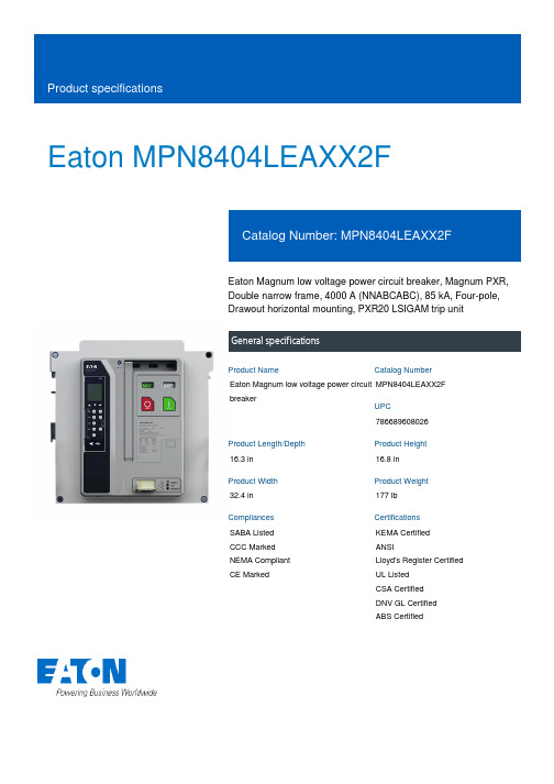
Eaton MPN8404LEAXX2FEaton Magnum low voltage power circuit breaker, Magnum PXR,Double narrow frame, 4000 A (NNABCABC), 85 kA, Four-pole,Drawout horizontal mounting, PXR20 LSIGAM trip unitGeneral specificationsEaton Magnum low voltage power circuitbreakerMPN8404LEAXX2F78668960802616.3 in16.8 in32.4 in177 lbSABA Listed CCC Marked NEMA Compliant CE Marked KEMA CertifiedANSILloyd's Register Certified UL ListedCSA CertifiedDNV GL CertifiedABS CertifiedProduct Name Catalog NumberUPCProduct Length/Depth Product Height Product Width Product Weight Compliances CertificationsDouble narrow Four-pole Magnum PXRDouble narrow Magnum PXR20 LSIG ARMSFour-pole4000 A85 kAIC85 kAIC4000 AZone selective interlocking application paper Magnum circuit breakers with Power Xpert Release trip units product aid Selevctive coordination application paper - IA0120000E3Magnum PXR and PD-SB double and double narrow frame UL Certificate of ComplianceMagnum PXR and PD-SB standard and narrow frame UL Certificate of CompliancePower Xpert Release trip unit for Magnum PXR circuit breakers PXR 20/25 user manualMagnum PXR low voltage power circuit breakers user manual Microsoft Word - Power Xpert Protection Manager Quick StartFrame Number of poles TypeFrame Series Trip TypeNumber of poles Rated uninterrupted current (Iu)Interrupt rating Interrupt rating Rated uninterrupted current (Iu)Application notesBrochuresCatalogsCertification reportsManuals and user guidesEaton Corporation plc Eaton House30 Pembroke Road Dublin 4, Ireland © 2023 Eaton. All Rights Reserved. Eaton is a registered trademark.All other trademarks areproperty of their respectiveowners./socialmediaGuide.docxPower Xpert Protection Manager x32 22.06 1 Power Xpert Protection Manager x64 22.6 1 Eaton Specification Sheet - MPN8404LEAXX2F Low voltage circuit breakers guide spec Magnum PXR 20/25 electronic trip units time current curves Cyber security white paperMolded case and low-voltage power circuit breaker health Safer by design: arc energy reduction techniquesSoftware, firmware, and applications Specifications and datasheetsTime/current curvesWhite papers。
- 1、下载文档前请自行甄别文档内容的完整性,平台不提供额外的编辑、内容补充、找答案等附加服务。
- 2、"仅部分预览"的文档,不可在线预览部分如存在完整性等问题,可反馈申请退款(可完整预览的文档不适用该条件!)。
- 3、如文档侵犯您的权益,请联系客服反馈,我们会尽快为您处理(人工客服工作时间:9:00-18:30)。
Avalanche Characteristics
Parameter
EAS IAR EAR Single Pulse Avalanche Energy Avalanche Current Repetitive Avalanche Energy
Typ.
––– ––– –––
Max.
510 8.0 13
2
IRF840A
100
100
VGS 15V 10V 8.0V 7.0V 6.0V 5.5V 5.0V BOTTOM 4.5V TOP
I D , Drain-to-Source Current (A)
I D , Drain-to-Source Current (A)
VGS 15V 10V 8.0V 7.0V 6.0V 5.5V 5.0V BOTTOM 4.5V TOP
2.5
10
TJ = 150 ° C
2.0
TJ = 25 ° C
1
1.5
1.0
0.5
0.1 4.0
V DS = 50V 20µs PULSE WIDTH 5.0 6.0 7.0 8.0 9.0
0.0 -60 -40 -20
VGS = 10V
0 20 40 60 80 100 120 140 160
VGS , Gate-to-Source Voltage (V)
Typ.
––– 0.50
Max.
1.0 ––– 62
Units
°C/W
Diode Characteristics
Min. Typ. Max. Units IS
I SM
VSD t rr Q rr ton
Conditions D MOSFET symbol ––– ––– 8.0 showing the A G integral reverse ––– ––– 32 S p-n junction diode. ––– ––– 2.0 V TJ = 25°C, IS = 8.0A, VGS = 0V ––– 422 633 ns TJ = 25°C, IF = 8.0A ––– 2.0 3.0 µC di/dt = 100A/µs Intrinsic turn-on time is negligible (turn-on is dominated by LS+LD)
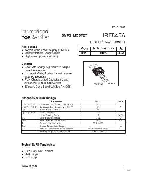
PD- 91900A
SMPS MOSFET
IRF840A
HEXFET® Poቤተ መጻሕፍቲ ባይዱer MOSFET
Applications l Switch Mode Power Supply ( SMPS ) l Uninterruptable Power Supply l High speed power switching Benefits Low Gate Charge Qg results in Simple Drive Requirement l Improved Gate, Avalanche and dynamic dv/dt Ruggedness l Fully Characterized Capacitance and Avalanche Voltage and Current l Effective Coss Specified (See AN1001)
Dynamic @ TJ = 25°C (unless otherwise specified)
gfs Qg Qgs Qgd td(on) tr td(off) tf Ciss Coss Crss Coss Coss Coss eff. Parameter Forward Transconductance Total Gate Charge Gate-to-Source Charge Gate-to-Drain ("Miller") Charge Turn-On Delay Time Rise Time Turn-Off Delay Time Fall Time Input Capacitance Output Capacitance Reverse Transfer Capacitance Output Capacitance Output Capacitance Effective Output Capacitance Min. 3.7 ––– ––– ––– ––– ––– ––– ––– ––– ––– ––– ––– ––– ––– Typ. ––– ––– ––– ––– 11 23 26 19 1018 155 8.0 1490 42 56 Max. Units Conditions ––– S VDS = 50V, ID = 4.8A 38 ID = 8.0A 9.0 nC VDS = 400V 18 VGS = 10V, See Fig. 6 and 13 ––– VDD = 250V ––– ID = 8.0A ns ––– RG = 9.1Ω ––– RD = 31Ω,See Fig. 10 ––– VGS = 0V ––– VDS = 25V ––– pF ƒ = 1.0MHz, See Fig. 5 ––– VGS = 0V, VDS = 1.0V, ƒ = 1.0MHz ––– VGS = 0V, VDS = 400V, ƒ = 1.0MHz ––– VGS = 0V, VDS = 0V to 400V
1000
Ciss
12
100
Coss
8
10
Crss
4
1 1 10 100 1000
0 0 10 20
FOR TEST CIRCUIT SEE FIGURE 13
30 40
VDS, Drain-to-Source Voltage (V)
Q G , Total Gate Charge (nC)
Fig 5. Typical Capacitance Vs. Drain-to-Source Voltage
10000
VGS = 0V, f = 1 MHZ Ciss = C + C , C gs gd ds SHORTED Crss = C gd Coss = C + Cgd ds
8.0 ID = 7.4 A
16
V DS = 400V V DS = 250V V DS = 100V
C, Capacitance(pF)
Max.
8.0 5.1 32 125 1.0 ± 30 5.0 -55 to + 150 300 (1.6mm from case ) 10 lbf•in (1.1N•m)
Units
A W W/°C V V/ns °C
Typical SMPS Topologies:
l l l
Two Transistor Forward Haft Bridge Full Bridge 1
l
VDSS
500V
Rds(on) max
0.85Ω
ID
8.0A
TO-220AB
G DS
Absolute Maximum Ratings
Parameter
ID @ TC = 25°C ID @ TC = 100°C IDM PD @TC = 25°C VGS dv/dt TJ TSTG Continuous Drain Current, VGS @ 10V Continuous Drain Current, VGS @ 10V Pulsed Drain Current Power Dissipation Linear Derating Factor Gate-to-Source Voltage Peak Diode Recovery dv/dt Operating Junction and Storage Temperature Range Soldering Temperature, for 10 seconds Mounting torqe, 6-32 or M3 screw
Fig 6. Typical Gate Charge Vs. Gate-to-Source Voltage
100
100
OPERATION IN THIS AREA LIMITED BY RDS(on)
ISD , Reverse Drain Current (A)
10us
10
TJ = 150 ° C
I D , Drain Current (A)
10 100us
1ms 1 10ms
1
TJ = 25 ° C
0.1 0.2
V GS = 0 V
0.5 0.8 1.1 1.4
0.1
TC = 25 °C TJ = 150 °C Single Pulse
10 100 1000 10000
VSD ,Source-to-Drain Voltage (V)
VDS , Drain-to-Source Voltage (V)
Units
mJ A mJ
Thermal Resistance
Parameter
RθJC RθCS RθJA Junction-to-Case Case-to-Sink, Flat, Greased Surface Junction-to-Ambient Parameter Continuous Source Current (Body Diode) Pulsed Source Current (Body Diode) Diode Forward Voltage Reverse Recovery Time Reverse RecoveryCharge Forward Turn-On Time
TJ , Junction Temperature ( °C)
Fig 3. Typical Transfer Characteristics
