CTDS1608C-222中文资料
BYC8-600中文资料
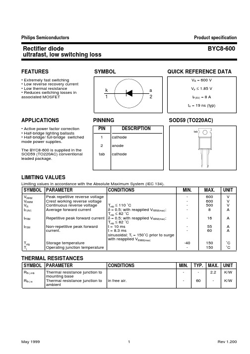
Philips Semiconductors Product specificationRectifier diodeBYC8-600ultrafast, low switching lossFEATURESSYMBOL QUICK REFERENCE DATA• Extremely fast switching• Low reverse recovery current • Low thermal resistance• Reduces switching losses in associated MOSFETAPPLICATIONSPINNINGSOD59 (TO220AC)• Active power factor correction PIN DESCRIPTION • Half-bridge lighting ballasts• Half-bridge/ full-bridge switched 1cathode mode power supplies.2anode The BYC8-600 is supplied in the SOD59 (TO220AC) conventional tabcathodeleaded package.LIMITING VALUESLimiting values in accordance with the Absolute Maximum System (IEC 134).SYMBOL PARAMETERCONDITIONSMIN.MAX.UNIT V RRM Peak repetitive reverse voltage -600V V RWM Crest working reverse voltage -600V V R Continuous reverse voltage T mb ≤ 110 ˚C-500V I F(AV)Average forward currentδ = 0.5; with reapplied V RRM(max);-8A T mb ≤ 82 ˚CI FRM Repetitive peak forward current δ = 0.5; with reapplied V RRM(max);-16A T mb ≤ 82 ˚CI FSMNon-repetitive peak forward t = 10 ms -55A current.t = 8.3 ms-60A sinusoidal; T j = 150˚C prior to surge with reapplied V RWM(max)T stg Storage temperature-40150˚C T jOperating junction temperature-150˚CTHERMAL RESISTANCESSYMBOL PARAMETERCONDITIONS MIN.TYP.MAX.UNIT R th j-mb Thermal resistance junction to -- 2.2K/W mounting baseR th j-aThermal resistance junction to in free air.-60-K/Wambient1tab2Philips Semiconductors Product specificationRectifier diodeBYC8-600ultrafast, low switching lossELECTRICAL CHARACTERISTICST j = 25 ˚C unless otherwise stated SYMBOL PARAMETER CONDITIONSMIN.TYP.MAX.UNIT V F Forward voltage I F = 8 A; T j = 150˚C - 1.4 1.85V I F = 16 A; T j = 150˚C - 1.7 2.3V I F = 8 A;- 2.0 2.8V I R Reverse current V R = 600 V-9150µA V R = 500 V; T j = 100 ˚C- 1.1 3.0mA t rr Reverse recovery time I F = 1 A; V R = 30 V; dI F /dt = 50 A/µs -3052ns t rr Reverse recovery time I F = 8 A; V R = 400 V;-19-ns dI F /dt = 500 A/µs t rr Reverse recovery time I F = 8 A; V R = 400 V;-3240ns dI F /dt = 500 A/µs; T j = 125˚C I rrm Peak reverse recovery current I F = 8 A; V R = 400 V;- 1.5 5.5A dI F /dt = 50 A/µs; T j = 125˚C I rrm Peak reverse recovery current I F = 8 A; V R = 400 V;-9.512A dI F /dt = 500 A/µs; T j = 125˚C V frForward recovery voltageI F = 10 A; dI F /dt = 100 A/µs-810VPhilips Semiconductors Product specificationRectifier diodeBYC8-600ultrafast, low switching lossPhilips Semiconductors Product specificationRectifier diodeBYC8-600ultrafast, low switching lossPhilips Semiconductors Product specificationRectifier diodeBYC8-600ultrafast, low switching lossMECHANICAL DATANotes1. Refer to mounting instructions for TO220 envelopes.2. Epoxy meets UL94 V0 at 1/8".Philips Semiconductors Product specification Rectifier diode BYC8-600 ultrafast, low switching lossDEFINITIONSData sheet statusObjective specification This data sheet contains target or goal specifications for product development. Preliminary specification This data sheet contains preliminary data; supplementary data may be published later. Product specification This data sheet contains final product specifications.Limiting valuesLimiting values are given in accordance with the Absolute Maximum Rating System (IEC 134). Stress above one or more of the limiting values may cause permanent damage to the device. These are stress ratings only and operation of the device at these or at any other conditions above those given in the Characteristics sections ofthis specification is not implied. Exposure to limiting values for extended periods may affect device reliability. Application informationWhere application information is given, it is advisory and does not form part of the specification.© Philips Electronics N.V. 1999All rights are reserved. Reproduction in whole or in part is prohibited without the prior written consent of the copyright owner.The information presented in this document does not form part of any quotation or contract, it is believed to be accurate and reliable and may be changed without notice. No liability will be accepted by the publisher for any consequence of its use. Publication thereof does not convey nor imply any license under patent or other industrial or intellectual property rights.LIFE SUPPORT APPLICATIONSThese products are not designed for use in life support appliances, devices or systems where malfunction of these products can be reasonably expected to result in personal injury. Philips customers using or selling these products for use in such applications do so at their own risk and agree to fully indemnify Philips for any damages resulting from such improper use or sale.。
DXI800 中文手册
2005 Beckman Coulter, Inc. P/N 986266E 3/05
i
UniCel DxI 800 使用说明
目录
4 样品架和样品容器 . . . . . . . . . . . . . . . . . . . . . . . . . . . . . . . . . . . . . . . . . . .4-1
本手册与 UniCel DxI Access 免疫分析系统 一同使用。
Access、 AccuTnI、 DxI、 Hybritech、 Ostase、 UniCel 以及 BECKMAN COULTER 徽标是 Beckman Coulter, Inc. 的商标
UniCel DxI 800 使用说明
2 关闭和重新启动 . . . . . . . . . . . . . . . . . . . . . . . . . . . . . . . . . . . . . . . . . . . . .2-1
ADIS16228加速度传感器手册
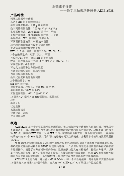
亚德诺半导体——数字三轴振动传感器ADIS16228 产品特性频域三轴振动传感器高达5 kHz的平坦频率响应数字加速度数据,±18 g测量范围数字测量范围设置:0至1g/ 10 g/ 10 g/20 g实时采样模式:20.48 kSPS 采样率,单轴采集样本模式:20.48 kSPS 采样率,三个轴触发模式:SPI,定时器,外部中断可编程抽取滤波器,11种速率设置对于选定的过滤器可设置多记录捕获手动捕获模式时域数据采集FFT,512点,实值,所有三个轴(X,Y,Z)3个窗函数选项:矩形,汉宁,平顶可编程FFT平均:高达255的平均次数贮存:可存储所有三个轴14个FFT记录(X,Y,Z)可编程报警,6个谱带可定义2级的警告和故障设置可调节的响应延迟,以减少误报内部自检与状态标志数字式温度和电源电压测量2个辅助数字I / OSPI兼容串行接口识别寄存器:序列号,设备ID,用户ID单电源供电:3.0 V至3.6 V工作温度范围:-40°C至+125°C15毫米×24毫米×15 mm铝封装,柔性接头应用振动分析状态监测机器运行状况仪器仪表,诊断安全切断传感概述ADIS16228是一个完整的振动监测测系统,集三轴加速度传感器和先进的时域、频域信号处理算法于一体。
时域的信号处理包括可编程抽取滤波器和可选的窗函数。
频域处理包括每个轴512点,实值的FFT变化,采用FFT平均,降低噪声本底变化,从而提高分辨率。
根据存储系统中的14个FFT记录,用户可以追踪随时间发生的变化,并利用多个抽取滤波器设置捕获FFT。
20.48 kSPS的采样速率和5 kHz的平坦频段提供的频率响应适合许多机械设备的健康应用。
铝芯提供优异的机械耦合到MEMS加速度传感器。
一个内部时钟驱动系统所有的数据采样和信号处理操作,消除了对外部时钟源的依赖。
数据捕获功能具有三种模式,提供多种选择,以满足不同应用的需要。
DS1632J-8中文资料
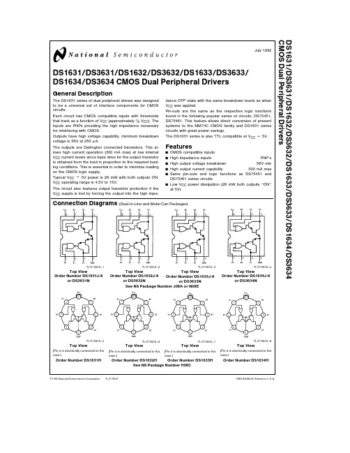
TL F 5816DS1631 DS3631 DS1632 DS3632 DS1633 DS3633 DS1634 DS3634CMOS Dual Peripheral DriversJuly 1992DS1631 DS3631 DS1632 DS3632 DS1633 DS3633 DS1634 DS3634CMOS Dual Peripheral DriversGeneral DescriptionThe DS1631series of dual peripheral drivers was designed to be a universal set of interface components for CMOS circuitsEach circuit has CMOS compatible inputs with thresholds that track as a function of V CC (approximately V CC ) The inputs are PNPs providing the high impedance necessary for interfacing with CMOSOutputs have high voltage capability minimum breakdown voltage is 56V at 250m AThe outputs are Darlington connected transistors This al-lows high current operation (300mA max)at low internal V CC current levels since base drive for the output transistor is obtained from the load in proportion to the required load-ing conditions This is essential in order to minimize loading on the CMOS logic supplyTypical V CC e 5V power is 28mW with both outputs ON V CC operating range is 4 5V to 15VThe circuit also features output transistor protection if the V CC supply is lost by forcing the output into the high impe-dance OFF state with the same breakdown levels as when V CC was appliedPin-outs are the same as the respective logic functions found in the following popular series of circuits DS75451 DS75461 This feature allows direct conversion of present systems to the MM74C CMOS family and DS1631series circuits with great power savingsThe DS1631series is also TTL compatible at V CC e 5VFeaturesY CMOS compatible inputs Y High impedance inputs PNP’s Y High output voltage breakdown 56V min Y High output current capability 300mA max YSame pin-outs and logic functions as DS75451and DS75461series circuitsYLow V CC power dissipation (28mW both outputs ‘‘ON’’at 5V)Connection Diagrams (Dual-In-Line and Metal Can Packages)TL F 5816–1Top ViewOrder Number DS1631J-8or DS3631NTL F 5816–2Top View Order Number DS1632J-8or DS3632N TL F 5816–3Top ViewOrder Number DS1633J-8or DS3633N TL F 5816–4Top ViewOrder Number DS1634J-8or DS3634NSee NS Package Number J08A or N08ETL F 5816–5Top View(Pin 4is electrically connected to the case )Order Number DS1631HTL F 5816–6Top View(Pin 4is electrically connected to the case )Order Number DS1632H TL F 5816–7Top View(Pin 4is electrically connected to the case )Order Number DS1633HTL F 5816–8Top View(Pin 4is electrically connected to the case )Order Number DS1634HSee NS Package Number H08CC 1995National Semiconductor Corporation RRD-B30M105 Printed in U S AAbsolute Maximum Ratings(Note1)If Military Aerospace specified devices are required please contact the National Semiconductor Sales Office Distributors for availability and specifications Supply Voltage16V Voltage at Inputs b0 3V to V CC a0 3V Output Voltage56V Storage Temperature Range b65 C to a150 C Maximum Power Dissipation at25 CCavity Package1133mW Molded Package1022mW TO-5Package787mW Lead Temperature(Soldering 4sec 260 C Derate cavity package7 6mW C above25 C derate molded package 8 2mW C above25 C derate TO-5package5 2mW C above25 C Operating ConditionsMin Max Units Supply Voltage V CCDS1631 DS1632 4 515V DS1633 DS1634DS3631 DS3632 4 7515V DS3633 DS3634Temperature T ADS1631 DS1632 b55a125 C DS1633 DS1634DS3631 DS3632 0a70 C DS3633 DS3634Electrical Characteristics(Notes2and3)Symbol Parameter Conditions Min Typ Max Units ALL CIRCUITSV IH Logical‘‘1’’Input Voltage(Figure1)V CC e5V3 52 5VV CC e10V8 05VV CC e15V12 57 5V V IL Logical‘‘0’’Input Voltage(Figure1)V CC e5V2 51 5VV CC e10V5 52 0VV CC e15V7 52 5V I IH Logical‘‘1’’Input Current V CC e15V V IN e15V (Figure2)0 110m A I IL Logical‘‘0’’Input Current V IN e0 4V (Figure3)V CC e5V b50b120m AV CC e15V b200b360m A V OH Output Breakdown Voltage V CC e15V I OH e250m A (Figure1)5665V V OL Output Low Voltage V CC e Min (Figure1)DS1631 DS1632 I OL e100mA0 851 1VDS1633 DS1634IOL e300mA1 11 4VV CC e Min (Figure1)DS3631 DS3632 I OL e100mA0 851 0VDS3633 DS3634IOL e300mA1 11 3V DS1631 DS3631I CC(0)Supply Currents V IN e0V (Figure4)V CC e5V Output Low711mAV CC e15V Both Drivers1420mA I CC(1)(Figure4)V CC e5V V IN e5V Output High23mAV CC e15V V IN e15V Both Drivers7 510mA t PD1Propagation to‘‘1’’V CC e5V T A e25 C C L e15pF R L e50X V L e10V 500ns(Figure5)t PD0Propagation to‘‘0’’V CC e5V T A e25 C C L e15pF R L e50X V L e10V 750ns(Figure5)DS1632 DS3632I CC(0)Supply Currents(Figure4)V CC e5V V IN e5VOutput Low 812mAV CC e15V V IN e15V1823mAI CC(1)V IN e0V (Figure4)V CC e5VOutput High 2 53 5mAV CC e15V914mA t PD1Propagation to‘‘1’’V CC e5V T A e25 C C L e15pF R L e50X V L e10V 500ns(Figure5)t PD0Propagation to‘‘0’’V CC e5V T A e25 C C L e15pF R L e50X V L e10V 750ns(Figure5)2Electrical Characteristics (Notes 2and 3)(Continued)Symbol Parameter Conditions MinTyp Max Units DS1633 DS3633I CC(0)Supply CurrentsV IN e 0V (Figure 4)V CC e 5V Output Low7 512mA V CC e 15V1623mA I CC(1)(Figure 4)V CC e 5V V IN e 5V Output High 24mA V CC e 15V V IN e 15V7 215mA t PD1Propagation to ‘‘1’’V CC e 5V T A e 25 C C L e 15pF R L e 50X V L e 10V 500ns (Figure 5)t PD0Propagation to ‘‘0’’V CC e 5V T A e 25 C C L e 15pF R L e 50X V L e 10V 750ns(Figure 5)DS1634 DS3634I CC(0)Supply Currents(Figure 4)V CC e 5V V IN e 5V Output Low 7 512mA V CC e 15V V IN e 15V 1823mA I CC(1)V IN e 0V (Figure 4)V CC e 5V Output High35mA V CC e 15V1118mA t PD1Propagation to ‘‘1’’V CC e 5V T A e 25 C C L e 15pF R L e 50X V L e 10V 500ns (Figure 5)t PD0Propagation to ‘‘0’’V CC e 5V T A e 25 C C L e 15pF R L e 50X V L e 10V 750ns(Figure 5)Note 1 ‘‘Absolute Maximum Ratings’’are those values beyond which the safety of the device cannot be guaranteed Except for ‘‘Operating Temperature Range’’they are not meant to imply that the devices should be operated at these limits The table of ‘‘Electrical Characteristics’’provides conditions for actual device operationNote 2 Unless otherwise specified min max limits apply across the b 55 C to a 125 C temperature range for the DS1631 DS1632 DS1633and DS1634and across the 0 C to a 70 C range for the DS3631 DS3632 DS3633and DS3634 All typical values are for T A e 25 CNote 3 All currents into device pins shown as positive out of device pins as negative all voltages referenced to ground unless otherwise noted All values shown as max or min on absolute value basisTest CircuitsTL F 5816–9Input Other Output Circuit Under Input Apply Measure Test DS3631V IH V IH I OH V OH V IL V CC I OL V OL DS3632V IH V IH I OL V OL V IL V CC I OH V OH DS3633V IH GND I OH V OH V IL V IL I OL V OL DS3634V IH GND I OL V OL V ILV ILI OHV OHNote Each input is tested separatelyFIGURE 1 V IH V IL V OH V OL3Test Circuits (Continued)TL F 5816–10Each input is tested separatelyFIGURE 2 I IHTL F 5816–11Note A Each input is tested separatelyNote B When testing DS1633and DS1634input not under test is grounded For all other circuits it is at V CCFIGURE 3 I ILTL F 5816–12Both gates are tested simultaneouslyFIGURE 4 I CC for AND and NAND CircuitsSchematic Diagram (Equivalent Circuit)TL F 5816–154Switching Time WaveformsTL F 5816–13TL F 5816–14 Note1 The pulse generator has the following characteristics PRR e500kHz Z OUT 50XNote2 C L includes probe and jig capacitanceFIGURE5 Switching Times5Physical Dimensions inches(millimeters)Metal Can Package(H)Order Number DS1631H DS1632H DS1633H or DS1634HNS Package Number H08C6Physical Dimensions inches(millimeters)(Continued)Ceramic Dual-In-Line Package(J)Order Number DS1631J-8 DS1632J-8 DS1633J-8or DS1634J-8NS Package Number J08A7D S 1631 D S 3631 D S 1632 D S 3632 D S 1633 D S 3633 D S 1634 D S 3634C M O S D u a l P e r i p h e r a l D r i v e r sPhysical Dimensions inches (millimeters)(Continued)Molded Dual-In-Line Package (N)Order Number DS3631N DS3632NDS3633N and DS3634N NS Package Number N08ELIFE SUPPORT POLICYNATIONAL’S PRODUCTS ARE NOT AUTHORIZED FOR USE AS CRITICAL COMPONENTS IN LIFE SUPPORT DEVICES OR SYSTEMS WITHOUT THE EXPRESS WRITTEN APPROVAL OF THE PRESIDENT OF NATIONAL SEMICONDUCTOR CORPORATION As used herein 1 Life support devices or systems are devices or 2 A critical component is any component of a life systems which (a)are intended for surgical implant support device or system whose failure to perform can into the body or (b)support or sustain life and whose be reasonably expected to cause the failure of the life failure to perform when properly used in accordance support device or system or to affect its safety or with instructions for use provided in the labeling can effectivenessbe reasonably expected to result in a significant injury to the userNational Semiconductor National Semiconductor National Semiconductor National Semiconductor CorporationEuropeHong Kong LtdJapan Ltd1111West Bardin RoadFax (a 49)0-180-530858613th Floor Straight Block Tel 81-043-299-2309。
CSC-161 系列数字式线路保护装置说明书
1.1 CSC-160 系列保护装置适用范围........................................................................... 1 1.2 CSC-160 系列保护装置主要特点........................................................................... 3 1.3 装置外形尺寸和安装尺寸...................................................................................... 4 1.4 装置外观.................................................................................................................. 5 1.5 装置执行的标准...................................................................................................... 5 1.6 CSC-161 系列装置的适用范围............................................................................... 5 1.7 本说明书适用范围.................................................................................................. 5
98822中文资料

Symbol Test Conditions Maximum RatingsV DSS T J = 25°C to 150°C800V V DGR T J = 25°C to 150°C; R GS = 1 M Ω800V V GS Continuous ±20V V GSM Transient ±30V I D25T C = 25°C750mA I DM T C = 25°C, pulse width limited by T JM3A I AR 1.0A E AR T C = 25°C 5mJ E AS T C = 25°C100mJ dv/dt I S ≤ I DM , di/dt ≤ 100 A/µs, V DD ≤ V DSS ,3V/ns T J ≤ 150°C, R G = 47 ΩP D T C = 25°C40W T J -55 ... +150°C T JM 150°C T stg -55 ... +150°CM d Mounting torque 1.13/10Nm/lb.in.WeightTO-220 4 g TO-252 0.8g TO-263 3gMaximum lead temperature for soldering 300°C1.6 mm (0.062 in.) from case for 10 s High Voltage MOSFETG = Gate, D = Drain,S = Source,TAB = DrainD (TAB)SymbolTest ConditionsCharacteristic Values(T J = 25°C, unless otherwise specified)min.typ.max.V DSS V GS = 0 V, I D = 250 µA 800V V GS(th)V DS = V GS , I D = 25 µA 2.54.5V I GSS V GS = ±20 V DC , V DS = 0±100nA I DSS V DS = V DSS T J = 25°C 25µA V GS = 0 VT J = 125°C500µA R DS(on)V GS = 10 V, I D = 500 mA9.511ΩPulse test, t ≤ 300 µs, duty cycle d ≤ 2 %Features!International standard packages !High voltage, Low R DS (on) HDMOS TMprocess!Rugged polysilicon gate cell structure!Fast switching timesApplications!Switch-mode and resonant-mode power supplies !Flyback inverters!DC choppers!High frequency matchingAdvantages !Space savings !High power densityDS98822C(11/03)TO-220AB (IXTP)© 2003 IXYS All rights reservedGSN-Channel Enhancement Mode Avalanche Energy Rated IXTA 1N80IXTP 1N80IXTY 1N80V DSS =800V I D25=750m A R DS(on)=11ΩPreliminary DataGSIXYS reserves the right to change limits, test conditions, and dimensions.IXYS MOSFETs and IGBTs are covered by one or more of the following U.S. patents:4,835,5924,881,1065,017,5085,049,9615,187,1175,486,7156,306,728B14,850,0724,931,8445,034,7965,063,3075,237,4815,381,025SymbolTest ConditionsCharacteristic Values(T J = 25°C, unless otherwise specified)min.typ.max.g fs V DS = 20 V; I D = 500 mA, pulse test0.70.8S C iss 220pF C oss V GS = 0 V, V DS = 25 V, f = 1 MHz23pF C rss 4pF t d(on)11ns t r V GS = 10 V, V DS = 0.5 • V DSS , I D = 1A 19ns t d(off)R G= 47Ω, (External)40ns t f 28ns Q G(on)8.5nC Q GS V GS = 10 V, V DS = 0.5 • V DSS , I D = 1A2.5nC Q GD 4.5nC R thJC 3.1K/W R thCK(IXTP)0.50K/WSource-Drain Diode Characteristic Values(T J = 25°C, unless otherwise specified)Symbol Test Conditions min.typ.max.I S V GS = 0 V750mA I SM Repetitive; pulse width limited by T JM 3A V SD I F = I S , V GS = 0 V,1.82V Pulse test, t ≤ 300 µs, duty cycle d ≤ 2 %t rrI F = I S , -di/dt = 100 A/µs, V R = 100 V710nsPins: 1 - Gate2 - Drain3 - Source4 - Drain Bottom SideTO-220 AD DimensionsTO-263 AA Outline1.Gate2.Drain3.Source4.DrainBottom Sidelimeter Inches Min.Max.Min.Max.A 4.06 4.83.160.190A1 2.03 2.79.080.110b 0.510.99.020.039b2 1.14 1.40.045.055c 0.460.74.018.029c2 1.14 1.40.045.055D 8.649.65.340.380D17.118.13.280.320E 9.6510.29.380.405E1 6.868.13.270.320e 2.54BSC .100BSC L 14.6115.88.575.625L1 2.29 2.79.090.110L2 1.02 1.40.040.055L3 1.27 1.78.050.070L400.380.015R0.460.74.018.029Dim. MillimeterInches Min.Max.Min.Max.A 2.19 2.380.0860.094A10.89 1.140.0350.045A200.1300.005b 0.640.890.0250.035b10.76 1.140.0300.045b2 5.21 5.460.2050.215c 0.460.580.0180.023c10.460.580.0180.023D 5.97 6.220.2350.245D1 4.32 5.210.1700.205E 6.35 6.730.2500.265E1 4.32 5.210.1700.205e 2.28 BSC 0.090 BSC e1 4.57 BSC 0.180 BSC H 9.4010.420.3700.410L 0.51 1.020.0200.040L10.64 1.020.0250.040L20.89 1.270.0350.050L32.54 2.920.1000.115TO-252 AA Outline。
NSSM016C中文资料

NSSM016C中⽂资料No. STSE-CM6044ASPECIFICATIONS FOR NICHIA CHIP TYPE FULL COLOR LEDMODEL : NSSM016CTNICHIA CORPORATION1.SPECIFICATIONS(1) Absolute Maximum Ratings (Ta=25°C)Absolute Maximum Rating Item Symbol Blue Green RedUnit Forward Current I F 35 35 50 mA Pulse Forward Current I FP 110 110 200 mA Reverse Voltage V R 5 V Power Dissipation P D 123 123 125 mW Total Power Dissipation P tot 280 mW Operating Temperature T opr -30 ~ + 85 °C Storage Temperature T stg -40 ~ +100 °C Soldering Temperature T sld Reflow Soldering : 260°C for 10sec.Hand Soldering : 350°C for 3sec.I FP Conditions : Pulse Width 10msec. and Duty 1/10 Value for one LED device (Single color).Value for total power dissipation when two and more devices are lit simultaneously.(2) Initial Electrical/Optical Characteristics (Ta=25°C)Blue Green Red Item Symbol Condition Typ.Max.Typ.Max. Typ. Max.UnitForward Voltage V FI F =20[mA] (3.2) 3.5 (3.2) 3.5 (2.1) 2.5 V Reverse Current I R V R = 5[V] - 50 - 50 - 50µA Luminous Intensity Iv I F =20[mA] (400)- (1200)- (700) - mcd x - I F =20[mA] 0.133- 0.189- 0.700 - - Chromaticity Coordinatey-I F =20[mA]0.075- 0.718- 0.299 - -Please refer to CIE 1931 chromaticity diagram.(3) Ranking(Ta=25°C)Blue Green Red Item Symbol Condition Min.Max.Min.Max. Min. Max.UnitLuminous IntensityIvI F =20[mA] 280 560 800 1600 380 1080mcdLuminous Intensity Measurement allowance is ± 10%.Color Ranks (I F =20mA, Ta=25°C)BlueRank Wx 0.139 0.129 0.113 0.1340.1450.152y 0.035 0.050 0.080 0.1050.0720.056GreenRank G0c x 0.166 0.136 0.176 0.2200.2370.201<= <=RedRRankx 0.674 0.648 0.677 0.708y 0.296 0.323 0.323 0.292Color Coordinates Measurement allowance is ± 0.01.2.INITIAL OPTICAL/ELECTRICAL CHARACTERISTICSPlease refer to figure’s page.3.OUTLINE DIMENSIONS AND MATERIALSPlease refer to figure’s page.Material as follows ; Package : Heat-Resistant PolymerPackage Upper Surface Color : BlackEncapsulating Resin : Epoxy Resin (Diffused)Electrodes: Ag Plating Copper Alloy4.PACKAGING· The LEDs are packed in cardboard boxes after taping.Please refer to figure’s page.The label on the minimum packing unit shows ; Part Number, Lot Number, Quantity· In order to protect the LEDs from mechanical shock, we pack them in cardboard boxes for transportation. · The LEDs may be damaged if the boxes are dropped or receive a strong impact against them,so precautions must be taken to prevent any damage.· The boxes are not water resistant and therefore must be kept away from water and moisture.· When the LEDs are transported, we recommend that you use the same packing method as Nichia.5.LOT NUMBERThe first six digits number shows lot number.The lot number is composed of the following characters;{ ¯¯¯¯{ - Year ( 5 for 2005, 6 for 2006 )- Month ( 1 for Jan., 9 for Sep., A for Oct., B for Nov. )¯¯¯¯ - Nichia's Product Number6.RELIABILITY(1) TEST ITEMS AND RESULTS Test ItemStandardTest MethodTest Conditions Note Number of DamagedResistance toSoldering Heat (Reflow Soldering) JEITA ED-4701300 301 Tsld=260°C, 10sec.(Pre treatment 30°C,70%,168hrs.) 2 times0/50Thermal Shock JEITA ED-4701300 307 0°C ~ 100°C 15sec. 15sec.100 cycles 0/50 Temperature CycleJEITA ED-4701100 105 -40°C ~ 25°C ~ 100°C ~ 25°C 30min. 5min. 30min. 5min. 100 cycles 0/50 Moisture Resistance Cyclic JEITA ED-4701200 203 25°C ~ 65°C ~ -10°C 90%RH 24hrs./1cycle 10 cycles 0/50 High Temperature Storage JEITA ED-4701200 201 Ta=100°C500hrs.0/50Temperature Humidity StorageJEITA ED-4701100 103 Ta=60°C, RH=90%500hrs. 0/50 Low Temperature Storage JEITA ED-4701200 202Ta=-40°C500hrs.0/50Steady State Operating LifeTa=25°C, B I F =13mA G I F =32mA R I F =21mA500hrs. 0/50Steady State Operating Life of High Humidity Heat60°C, RH=90%, B I F =8.5mA G I F =18mA R I F =14.5mA500hrs. 0/50Steady State Operating Life of Low TemperatureTa=-30°C,B I F =13mA G I F =32mA R I F =21mA500hrs. 0/50Value for one LED device (Single color).(2) CRITERIA FOR JUDGING DAMAGE (Value for one LED device (Single color).)Criteria for Judgement Item SymbolTest Conditions Min. Max. Forward Voltage V F B,G,R I F =20mA - U.S.L.*) 1.1 Reverse Current I R B,G,R V R =5V - U.S.L.*) 2.0 Luminous IntensityI VB,G,R I F =20mA L.S.L.**) 0.7 -*) U.S.L. : Upper Standard Level **) L.S.L. : Lower Standard Level7.CAUTIONS(1) Moisture Proof Package· When moisture is absorbed into the SMT package it may vaporize and expand during soldering.There is a possibility that this can cause exfoliation of the contacts and damage to the opticalcharacteristics of the LEDs. For this reason, the moisture proof package is used to keep moisture to a minimum in the package.· The moisture proof package is made of an aluminum moisture proof bag. A package ofa moisture absorbent material (silica gel) is inserted into the aluminum moisture proof bag.The silica gel changes its color from blue to pink as it absorbs moisture.(2) Storage· Storage ConditionsBefore opening the package :The LEDs should be kept at 30°C or less and 90%RH or less. The LEDs should be used within a year. When storing the LEDs, moisture proof packaging with absorbent material (silica gel) is recommended.After opening the package :The LEDs should be kept at 30°C or less and 70%RH or less. The LEDs should be solderedwithin 168 hours (7days) after opening the package. If unused LEDs remain, they should bestored in moisture proof packages, such as sealed containers with packages of moisture absorbent material (silica gel). It is also recommended to return the LEDs to the original moisture proof bag and to reseal the moisture proof bag again.· If the moisture absorbent material (silica gel) has faded away or the LEDs have exceeded the storage time, baking treatment should be performed using the following conditions.Baking treatment : more than 24 hours at 65 ± 5°C· Nichia LED electrodes are silver plated copper alloy. The silver surface may be affected byenvironments which contain corrosive substances. Please avoid conditions which may cause the LED to corrode, tarnish or discolor. This corrosion or discoloration may cause difficulty during soldering operations. It is recommended that the User use the LEDs as soon as possible.· Please avoid rapid transitions in ambient temperature, especially in high humidity environments where condensation can occur.(3) Heat Generation· Thermal design of the end product is of paramount importance. Please consider the heat generation of the LED when making the system design. The coefficient of temperature increase per inputelectric power is affected by the thermal resistance of the circuit board and density of LED placement on the board, as well as other components. It is necessary to avoid intense heat generation and operate within the maximum ratings given in this specification.· During operation of the LEDs the total power dissipation of the diode elements (red, green, and blue) within the LEDs must not exceed the maximum power dissipation.· The operating current should be decided after considering the ambient maximum temperature of LEDs.120sec.Max.Pre-heating 260°C Max.10sec. Max. 60sec.Max. Above 220°C 1 ~ 5°C / sec. 1 ~ 5°C / sec. 180 ~ 200°C <1 : Lead Solder> <2 : Lead-free Solder> Pre-heating 240°C Max.10sec. Max. 60sec.Max. Above 200°C2.5 ~ 5°C / sec.2.5 ~ 5°C / sec. 120 ~ 150°C 120sec.Max. Nichia STSE-CM6044A-1(4) Soldering Conditions· The LEDs can be soldered in place using the reflow soldering method. Nichia cannot make a guarantee on the LEDs after they have been assembled using the dip soldering method. · Recommended soldering conditionsReflow SolderingHand SolderingLead Solder Lead-free Solder Pre-heat Pre-heat time Peak temperature Soldering time Condition 120 ~ 150°C 120 sec. Max. 240°C Max. 10 sec. Max. refer to Temperature - profile 1. 180 ~ 200°C 120 sec. Max. 260°C Max. 10 sec. Max. refer to Temperature - profile 2.(N 2 reflow is recommended.)Temperature Soldering time 350°C Max. 3 sec. Max. (one time only)Although the recommended soldering conditions are specified in the above table, reflow or handsoldering at the lowest possible temperature is desirable for the LEDs.A rapid-rate process is not recommended for cooling the LEDs down from the peak temperature. [Temperature-profile (Surface of circuit board)] Use the conditions shown to the under figure.[Recommended soldering pad design] Use the following conditions shown in the figure.· Occasionally there is a brightness decrease caused by the influence of heat or ambient atmosphere during air reflow. It is recommended that the User use the nitrogen reflow method.· Repairing should not be done after the LEDs have been soldered. When repairing is unavoidable, a double-head soldering iron should be used. It should be confirmed beforehand whether the characteristics of the LEDs will or will not be damaged by repairing. · Reflow soldering should not be done more than two times. · When soldering, do not put stress on the LEDs during heating. · After soldering, do not warp the circuit board.(5) Cleaning· It is recommended that isopropyl alcohol be used as a solvent for cleaning the LEDs. When using other solvents, it should be confirmed beforehand whether the solvents will dissolve the package and the resin or not. Freon solvents should not be used to clean the LEDs because of worldwide regulations. · Do not clean the LEDs by the ultrasonic. When it is absolutely necessary, the influence of ultrasonic cleaning on the LEDs depends on factors such as ultrasonic power and the assembled condition. (Unit : mm)2.7538.751.731.71.45.6Nichia STSE-CM6044A-1(6) Static Electricity· Static electricity or surge voltage damages the Blue/Green LEDs.It is recommended that a wrist band or an anti-electrostatic glove be used when handling the LEDs.· All devices, equipment and machinery must be properly grounded. It is recommended that precautions be taken against surge voltage to the equipment that mounts the LEDs.· When inspecting the final products in which LEDs were assembled, it is recommended to checkwhether the assembled LEDs are damaged by static electricity or not. It is easy to findstatic-damaged LEDs by a light-on test or a VF test at a lower current (below 1mA is recommended). · Damaged LEDs will show some unusual characteristics such as the leak current remarkablyincreases, the forward voltage becomes lower, or the LEDs do not light at the low current.Criteria : (V F> 2.0V at I F=0.5mA)(7) Others· NSSM016C complies with RoHS Directive.· Care must be taken to ensure that the reverse voltage will not exceed the absolute maximum ratingwhen using the LEDs with matrix drive.· The LED light output is strong enough to injure human eyes. Precautions must be taken to prevent looking directly at the LEDs with unaided eyes for more than a few seconds.· Flashing lights have been known to cause discomfort in people; you can prevent this by takingprecautions during use. Also, people should be cautious when using equipment that has had LEDsincorporated into it.· The LEDs described in this brochure are intended to be used for ordinary electronic equipment (such as office equipment, communications equipment, measurement instruments and household appliances).Consult Nichia’s sales staff in advance for information on the applications in which exceptional quality and reliability are required, particularly when the failure or malfunction of the LEDs may directlyjeopardize life or health (such as for airplanes, aerospace, submersible repeaters, nuclear reactorcontrol systems, automobiles, traffic control equipment, life support systems and safety devices).· User shall not reverse engineer by disassembling or analysis of the LEDs without having prior written consent from Nichia. When defective LEDs are found, the User shall inform Nichia directly beforedisassembling or analysis.· The formal specifications must be exchanged and signed by both parties before large volume purchase begins. · The appearance and specifications of the product may be modified for improvement without notice.Nic hia STSE-CM 6044AColor Coordinates Measurement allowance is ± 0.01.元器件交易⽹/doc/c486e8d17f1922791688e8a3.htmlNichiaSTSE-CM6044ANichiaSTSE-CM6044A-2Nichia STSE-CM6044A-11-Nichia STSE-CM6044A元器件交易⽹/doc/c486e8d17f1922791688e8a3.html Nichia STSE-CM6044A。
S-80840CNMC-B8C-T2中文资料

Features
• Ultra-low current consumption • • • • • 1.3 µA typ. (detection voltage≤1.4 V, at VDD=1.5 V) 0.8 µA typ. (detection voltage≥1.5 V, at VDD=3.5 V) High-precision detection voltage ±2.0 % Operating voltage range 0.65 V to 5.0 V (detection voltage≤1.4 V) 0.95 V to 10.0 V (detection voltage≥1.5 V) Hysteresis characteristics 5 % typ. Detection voltage 0.8 V to 6.0 V (0.1 V step) Output form Nch open-drain output (Active Low) CMOS output (Active Low)
ULTRA-SMALL PACKAGE HIGH-PRECISION VOLTAGE DETECTOR S-808xxC Series
Product Name Structure
The detection voltage, output form and packages for S-808xxC Series can be selected at the user's request. Refer to the "1. Product Name" for the construction of the product name and "2. Product Name List" for the full product names. 1. Product Name 1-1. SC-82AB, SOT-23-5, SOT-89-3 packages
8122控制器
当火灾探测器通过回路总线LED灯点燃,液晶屏显示火警回路(或楼层)、部位(或房号),当有连续多个探测器报警时,显示屏除显示报警首地址外,重复显示后续报警地址和火警总数。按消音键,可切断火灾声响,但一旦控制器接收到新的火警信号时,系统则再次发出火警声响。
JB-TB-8122箱体设计为小容量报警系统,外型采用挂壁式薄型结构,适合挂壁式安装。备电电源采用单组24V,减少了箱体重量和体积,单机报警容量可从16点至126点,以适用于建筑面积为几百~几千平方米的报警场所。
本产品符合GB4717-93标准。
二、技术特性
⒈探测器回路为两总线制,可挂接带地址编码的烟温探测器、手动报警按钮、输入模块;
⒉探测器容量为2×63点;
⒊回路传输距离(双绞线)可达1500m;
⒋控制器具有RS232和RS485通信接口,通过跳线可将它们设置为:
RS232×1个口, RS485×1个口
或RS232×2个口
或RS485×2个口;
⒌系统连接区域机容量可达31台;
⒍采用双绞屏蔽线RS485通信距离可达1200m;
⒎RS232通信距离为17m;
⒊JB-TB-8122电源板
a) P1交流电源。
b) P2 6芯插头,为I/O板提供直流电源。
c) P3 2芯插头,为电池充电电源,红线接电池“+”极,黑线接电池“-”极。
六、运行和操作
⒈开机
拨好机箱地址,检查系统连线,合上电源开关,机器运行,手动联动和交流工作指示灯亮,液晶显示:
接着显示:
按“1”进入校时功能,按“2”进入下一步。
CT14
3C
NO
3号继电器常开触点
COM
3号继电器动触点
NC
1984222资料
PHOENIX CONTACT GmbH & Co. KG http://www.phoenixcontact.de
Page 3 / 3 Mar 9, 2008
Page 2 / 3 Mar 9, 2008
元器件交易网
PT 1,5/ 8-PVH-3,5-A Order No.: 1984222
http://eshop.phoenixcontact.de/phoenix/treeViewClick.do?UID=1984222
Address
Tools 1205037 SZS 0,4X2,5 Screwdriver, bladed, matches all screw terminal blocks up to 1.5 mm² connection cross section, blade: 0.4 x 2.5 mm
PHOENIX CONTACT GmbH & Co. KG http://www.phoenixcontract from the online catalog
PT 1,5/ 8-PVH-3,5-A
Order No.: 1984222
http://eshop.phoenixcontact.de/phoenix/treeViewClick.do?UID=1984222
Marking 0804073 SK 3,5/2,8:FORTL.ZAHLEN Marker card, printed horizontally, self-adhesive, 10-section marker strip, 14 identical decades marked 1-10, 11-20 etc. up to 91-100, sufficient for 140 terminal blocks
CR160中文资料

Current Regulator DiodesCR160CR220CR300CR390CR180CR240CR330CR430CR200CR270CR360CR470PRODUCT SUMMARYPart NumberTyp I F (mA)Min P OV(V)Part NumberTyp I F (mA)Min P OV(V)CR160 1.60100CR300 3.00100CR180 1.80100CR330 3.30100CR200 2.00100CR360 3.60100CR2202.20100CR3903.90100CR240 2.40100CR4304.30100CR2702.70100CR4704.70100FEATURESBENEFITS APPLICATIONSD Two-Lead Hermetic Package D Guaranteed Tight "10% ToleranceD Operation from 1 V (CR160) to 100 V DExcellent Temperature StabilityD Simple Series Circuitry, No Separate VoltageSource D Tighter Guaranteed Circuit PerformanceD Excellent Performance in Low-Voltage/Battery Circuits and High-Voltage Spike Protection D High Circuit Stability vs. TemperatureD Constant-Current Supply D Current-Limiting D Timing CircuitsDESCRIPTIONThe CR160 series is a family of "10% range current regulators designed for demanding applications in test equipment and instrumentation. These devices combine a JFET with an integrated resistor to produce a single two-leaded device which is extremely simple to operate. With nominal current ranges from 1.60 mA to 4.70 mA, this serieswill meet a wide array of design requirements.The TO-206AA hermetically sealed package is available with military processing per MIL-S-19500 (see Military Information).SCHEMATIC DIAGRAMAPPLICATIONSA For applications information see AN103.TO-206AA 2-LeadABSOLUTE MAXIMUM RATINGSPeak Operating Voltage100 V. . . . . . . . . . . . . . . . . . . . . . . . . . . . . . . . . . . . . . . Reverse Current50 mA . . . . . . . . . . . . . . . . . . . . . . . . . . . . . . . . . . . . . . . . . . . . .Thermal Resistance (q JA)417_C/W. . . . . . . . . . . . . . . . . . . . . . . . . . . . . . . . . . Storage Temperature −55 to 200_C. . . . . . . . . . . . . . . . . . . . . . . . . . . . . . . . . . .Power Dissipation a300 mW. . . . . . . . . . . . . . . . . . . . . . . . . . . . . . . . . . . . . . . . .Notes:a.Derate 2.4 mW/_C above 25_CSPECIFICATIONS (T A = 25_C UNLESS OTHERWISE NOTED)Limits Parameter Symbol Test Conditions Min Typ a Max UnitPeak Operating Voltage b P OV I F = 1.1 I F(max)100135Reverse Voltage V R I R = 1 mA0.8V Capacitance C F V F = 25 V, f = 1 MHz6pFRegulator Current c(I F)Dynamic Im-pedance d(Z d)KneeImpedance(Z k)LimitingVoltage e(V L)TemperatureCoefficient(q1)V F = 25 V V F = 25 V V F = 6 V I F = 0.8 I F(min)V F = 25 V0_C v T A v 100_CmA M W M W V ppm/_CPart Number Min Nom Max Min Typ a Min Typ a Max Typ a Typ a CR160 1.440 1.60 1.7600.475 1.100.0920.40 1.650.701000CR180 1.620 1.80 1.9800.420 1.000.0740.34 1.750.75650CR200 1.800 2.00 2.2000.3950.900.0610.28 1.850.80300CR220 1.980 2.20 2.4200.3700.830.0520.25 1.950.85100CR240 2.160 2.40 2.6400.3450.760.0440.22 2.000.900CR270 2.430 2.70 2.9700.3200.700.0350.19 2.150.95−200CR300 2.700 3.00 3.3000.3000.650.0290.16 2.25 1.00−400CR330 2.970 3.30 3.6300.2800.600.0240.14 2.35 1.05−550CR360 3.240 3.60 3.9600.2650.540.0200.13 2.50 1.10−730CR390 3.510 3.90 4.2900.2550.470.0170.12 2.60 1.17−820CR430 3.870 4.30 4.7300.2450.400.0140.10 2.75 1.25−1000CR470 4.230 4.70 5.1700.2350.350.0120.09 2.90 1.32−1125Notes:NKOa.Typical values are for DESIGN AID ONLY, not guaranteed nor subject to production testing.b.Peak voltage at which I F = 1.1 I F(max).c.Pulse test—steady state currents may vary.d.Pulse test—steady state impedances may vary.e.Min V F required to insure I F = 0.8 I F(min).TYPICAL CHARACTERISTICS (T A = 25_C UNLESS OTHERWISE NOTED)Output Current vs. Forward VoltageOutput Current vs. Forward VoltageDynamic Impedance vs. Regulator CurrentLimiting Voltage @ 0.8 Ivs. Regulator CurrentLimiting Current vs. TemperatureKnee Impedance vs. Regulator Current543001521234(V)F V6020100406080(V)F V T J (_C)−55−35−15525456585105125543021651010.10.0221I F (mA)51020.2211I F (mA)51020.2211I F (mA)0.050.20.50.50.5I F (m A )Z d (M Ω)Z k (M Ω)V L (V )I F (m A )TYPICAL CHARACTERISTICS (T A = 25_C UNLESS OTHERWISE NOTED)Temperature Coefficient vs. Regulator CurrentOn-resistance vs. Regulator CurrentCapacitance vs. Forward VoltageThermal Resistance vs. Power Dissipation51021I F (mA)0.250−0.25400100163002345200201612105084203040100200300400500100010010V F (V)I F (mA)P D (mW)T C (% _C )r D S (o n ) − D r a i n -S o u r c e O n -R e s i s t a n c e ( Ω )C T − T o t a l C a p a c i t a n c e (p F )q J R (_C /W )CURRENT REGULATOR DIODE V-1 CHARACTERISTICV RV FI。
DIN76722:2008(中文)

DIN76722:2008(中文)DIN 76722 :2008道路车辆—低压电缆—型号标识1 范围本标准适用于符合ISO 6722 和ISO 14572 标准的道路车辆用电线电缆。
规定了该电缆的型号标识。
2 规范性引用文件下列引用文件对于本文件的使用是不可或缺的。
对于所引用的文件,凡是注日期的引用, 只引用其被纳入的修正或修改。
凡是不注日期的引用,引用其最新版本(包括任何修订)。
DIN 72551-7 道路车辆–电压电线电缆–第7 部分: 低压电线颜色和颜色代码ISO 6722 道路车辆- 60 V和600 V 单芯电线电缆–尺寸、测试方法和要求ISO 14572 道路车辆–圆形,屏蔽和非屏蔽60 V和600 V 多芯护套电缆—基本和高性能电缆的测试方法和要求3 型号标识3.1 总则描述道路车辆低压电缆的标识代码的各段(型号字符),按以下结构组成。
3.2 基本代码字符型号标识都是以这两个字符开始:FL (=汽车电线电缆)按照电线电缆结构从内到外的顺序使用规定的标识代码字符。
3.3 导体材料导体材料采用以下标识字符,如果铜导体省略。
表1–导体材料标识意义AL 铝W 高电阻材料M 其它导体材料3.4 结构特征对于具体的结构特征的缩写字符是在FL和必要的导体材料之后。
如果需要几个特殊的结构功能,识别标记按字母按顺序标注。
表2–结构特征标识意义F 常规扁平电缆Z 多芯可分离电缆R 薄壁绝缘,符合ISO 6722 的薄壁(Thin wall)U 超薄壁绝缘,符合ISO 6722 的超薄壁(Ultra-thin wall)S 超厚壁绝缘,超过ISO 6722 的厚壁(Thick wall)3.5 绝缘和护套材料对于对应的绝缘材料的标识字符标注在结构特征和导体材料之后,如果这些都不存在,则直接标注在FL后面。
对于护套使用的标识字符,按照护套在电缆上的位置,按照从内到外的顺序标注相应的字符。
表 3 –热塑性塑料盒热塑性弹性体标识意义Y PVC (聚氯乙烯)02Y PE (发泡聚乙烯)2Y PE (聚乙烯)4Y PA (聚酰胺)5Y PTFE (聚四氟乙烯)6Y FEP (四氟乙烯/六氟丙烯共聚物)7Y E-TFE(乙烯/四氟乙烯共聚物)9Y PP (聚丙烯)09Y PP (发泡聚丙烯)10Y PVDF (聚偏氟乙烯)11Y TPE-U (PUR) (聚氨酯)12Y PBT (聚对苯二甲酸乙二醇酯)13Y TPE-E (聚酯弹性体)31Y TPE-S (苯乙烯嵌段共聚物)51Y PFA (全氟烷氧基烷烃)91Y TPE-O (热塑性聚烯烃弹性体)NY 非标热塑性塑料或热塑性弹性体注意: 当可以提供交联聚合物时,把各自字母“Y” 用“X”代替。
SC225中文资料

SMT - on ceramic technology Metal case Isolation I/O 500Veff EMI/RFI radiated EN55022-B Short circuit proof 100% burn-in and parameter test Switching frequency: 200kHz
ISO 9001 Registered
Sales office for Germany ELEKTRA REINSTADLER GmbH Arnbacherstr., 32 - 85247 Schwabhausen Germany Tel.: +49 08138 9161 - Fax.: +49 08138 8484 e-mail: elektra.reinstadler@t-online.de
Connections Pin 1 .................................... +Input Pin 2 ..................................... -Input Pin 3 ............................... +Output 1 Pin 4 ................................ -Output 1 Pin 5 ............................... +Output 2 Pin 6 ................................ -Output 2 Pin 7 ..................................... no pin
DC/DC Converter SC225
雅培生化系统C16000中文操作手册
ABBOTT
试剂容器:试剂容器放置于试剂转盘中,容器除放置检测试剂外,还可 以放置稀释清洗液,样品稀释液和水浴添加剂。容量和形状包括: 20ml,55ml,90ml,100ml 盒状和 20ml 瓶状。 1.2.3 标准品:包含单项和多项标准品,不同项目的相关试剂参数请参阅雅培生 化试剂参数表。每个项目上机可以保存 4 条不同批号的标准曲线。 1.2.4 ICT 模块:集成晶片技术,含钠、钾和氯。可保证做 15000 个样品 (45000 个测试),或至少 2 个月安装使用效期。 1.2.5 ICT 标准品:包括血清和尿二种类型,含低和高二个水平。详见雅培生化 试剂参数。 1.2.6 ICT 清洗液:仪器每日保养清洗 ICT 模块。 1.2.7 大瓶溶液:大瓶溶液包括 ICT 参比液,碱性液和酸性液 ICT 参比液:2000ml/瓶,为样品检测提供参比浓度。 碱性洗液:500ml/瓶,主要成份为 NaOH。用于反应杯清洗。 酸性洗液:500ml/瓶,主要成份为甲醇。用于反应杯清洗(稀释后可用 于样品/试剂探针和混匀器的清洗) 1.2.8 机上溶液:机上溶液为吸样探针,试剂探针,混匀器和反应杯清洗用的去 污剂。主要在一些特殊的清洗(SmartWash)模式时使用。有些是用于保养 程序。自定义放置于 R1 试剂仓(C1/2/3 和 D1/2/3 位)或 R2 试剂仓 (C1/2/3 和 D1/2/3 位),主要有: 0.5%酸性溶液(用酸性洗液进行 0.5%稀释),配制后上机稳定 30 天 去污剂 A,主要成份为 2-氨基乙醇 10%去污剂 B(用去污剂 B 进行 50%稀释),主要成份为 NaOH,配制 后上机稳定 30 天 1.2.9 水浴添加剂:用于抑制水浴槽中微生物的生长。放置于 R1 试剂仓 A1 位 置,每日仪器会自动加入。 1.3 系统主要附件 系统主要附件如下: 1.3.1 样品架:可同时放置不同类型的原试管,血清管和样品杯。每架有 5 个位 置,条型码识别样品架和样品管。 1.3.2 样品盘:放置样品架,每盘可放置 5 个样品架。 1.3.3 试剂分隔架:R1 试剂转盘含一个内圈的试剂分隔架(有 20 个试剂位)和 3 个外圈的试剂分隔架(分 12 个或 15 个试剂位)。R2 试剂转盘含 4 个外圈 的试剂分隔架(分 9 个或 14 个试剂位)。 1.3.4 试剂容器适配器:主要用于小包装试剂(如 20ml 和 55ml 的盒状试剂和 20ml 的瓶状试剂)在大试剂分隔架上的使用。分盒状和瓶状二种适配器。 1.4 系统自动冲洗对大瓶溶液的消耗 系统自动冲洗是为了保证管路中没有汽泡。在运行模块运行前和每 8 个小时会 进行冲洗。主要冲洗的大瓶溶液有 ICT 参比液(每次 2.75ml),碱性溶液(每次 0.06ml)和酸性溶液(每次 0.04ml)。
CS22中文资料

32IXYS reserves the right to change limits, test conditions and dimensionsPhase Control ThyristorsElectrically Isolated Tab V RSM V RRM TypeV DSM V DRM V V 800 800CS 22-08io1M 12001200CS 22-12io1MSymbol ConditionsMaximum RatingsI T(AV)M T C = 85°C 180° sine ①16A T A = 25°C 180° sine ② 2.5A I TSMT VJ = 45°C t = 10 ms (50 Hz), sine 300A V R = 0 V t = 8.3 ms (60 Hz), sine 340A T VJ = T VJM t = 10 ms (50 Hz), sine 250A V R = 0 Vt = 8.3 ms (60 Hz), sine 285A I 2tT VJ = 45°C t = 10 ms (50 Hz), sine 450A 2s V R = 0 V t = 8.3 ms (60 Hz), sine 480A 2s T VJ = T VJM t = 10 ms (50 Hz), sine 300A 2s V R = 0 Vt = 8.3 ms (60 Hz), sine337A 2s (di/dt)crT VJ = T VJM repetitive, I T = 20 A 150A/µsf = 50Hz, t P = 200µs V D = 2/3 V DRM I G = 0.08 A non repetitive, I T = I T(AV)M 500A/µs di G /dt = 0.08 A/µs(dv/dt)cr T VJ = T VJM , V DR = 2/3 V DRM1000V/µs R GK = ∞, method 1 (linear voltage rise)P GM T VJ = T VJM t P = 30 µs 10W I T = I T(AV)Mt P = 300 µs5W P GAV 0.5W V RGM 10V T VJ -40...+150°C T VJM 150°C T stg -40...+125°C M dMounting torque M 3 or UNC 4-400.5-0.8Nm Weight3gFeatures•Thyristor for frequencies up to 400Hz •International standard package •Epoxy meets UL 94V-0•High performance glass passivated chip •Long-term stability of leakage current and blocking voltage•Plasitc overmolded tab for electrical isolation Applications•Motor control •Power converter •AC power controller•Light and temperature control•SCR for inrush current limiting in power supplies or AC drive Advantages•Space and weight savings •Simple mountingACGV RRM = 800-1200 V I T(AV)M = 16 AA = Anode, C = Cathode, G = Gate Tab = Isolated0 IsolatedA AC ① mounted on heatsink Data according to IEC 60747② without heatsink32IXYS reserves the right to change limits, test conditions and dimensionsSymbol ConditionsCharacteristic ValuesI R , I D T VJ = T VJM , V R = V RRM , V D = V DRM ≤5mA V T I T= 30 A, T VJ = 25°C≤1.5V V T0For power-loss calculations only (T VJ = 150°C)0.9V r T 18m ΩV GT V D = 6 V T VJ = 25°C ≤ 1.5V T VJ = -40°C ≤ 2.5V I GT V D = 6 VT VJ = 25°C ≤30mA T VJ = -40°C≤50mA V GD T VJ = T VJM , V D = 2/3 V DRM≤0.2V I GD ≤3mA I L T VJ = 25°C, t P = 10 µs≤100mA I G = 0.08 A, di G /dt = 0.08 A/µs I H T VJ = 25°C, V D = 6 V, R GK =∞≤80mA t gd T VJ = 25°C, V D = ½ V DRM≤2µs I G = 0.08 A, di G /dt = 0.08 A/µs R thJC DC current 2.5K/W R thCH DC current 0.5K/W R thJA DC current50K/W aMax. acceleration, 50 Hz50m/s 2Package Outline。
CT 线材测试仪用户手册

e.插上治具连接好待测试线材样品(良品),按 Learn 键学习资 料,SAVE+Enter 存档。按 EXIT 跳离主画面。按 TEST 键即可测试
温湿度 摄氏 15℃~35℃ 相对湿度 RH≦75% 尺寸(宽*高*深) 425*190*350mm
高压绝缘测试 200~700Vdc;200~500Vac
重量 重约 14 公斤(不含配件)
50V Resolution ±5%准确度 显示/声响装置 320/240 解析度液晶圆形显示 Pass/Fail LED 红绿指示灯/书面显示/声响 量测接点 128 量测接点 可选购 256/512 接点 高压校正正负端输出(+/-)
控制面板 系统/快速/编辑/功能 按键群组
介面 RS-232 通讯连接埠 印表机埠 远端控制埠 记忆装置 Flash Memory 最多可储存 56 组测试设定档案
CT-8681 线材测试仪基本操作 :
文 字 数 字 输 入 :在 做 档 案 存 储 时 要 求 输 入 文 字 数 字 ,第 一 次 按 下 为该按键数字第 2—4 次分别代表数字键上方由左到右之大写英文字 母。
短断路表 档案:123
NET 短断路点位 页数 1/1 (6Nets)
001 A01 118
002 A02 120
003 A03 123
004 A04 121
005 A05 118
006 A06 121
