LED Driver_1696_5V700mA
AIP1640 TM1640中微爱芯LED显示驱动芯片
产品说明书1、概述AiP1640 是一款2 线串口共阴极8 段16 位的LED 驱动控制专用电路,内部集成有MCU 数字接口、数据锁存器、LED 驱动等电路。
本产品性能优良,质量可靠。
其主要特点如下:内置显示RAM内置RC振荡内置自动消隐电路显示辉度软件可调两线串行接口(CLK,DATA)封装形式:SOP28/SSOP28(0.635mm)应用领域:LED显示面板场合,例如电磁炉显示、电饭煲显示、空调显示、电子秤等家电产品。
订购信息:管装:产品型号封装形式打印标识管装数盒装管盒装数箱装盒箱装数备注说明AiP1640SA.TB SOP28 AiP1640 25PCS/管80 管/盒2000PCS/盒10 盒/箱20000PCS/箱塑封体尺寸:17.9mm×7.5mm 引脚间距:1.27mmAiP1640VB.TB SSOP28 AiP1640 50PCS/管200 管/盒10000PCS/盒 5 盒/箱50000PCS/箱塑封体尺寸:9.9mm×3.9mm引脚间距0.635mm编带:产品型号封装形式打印标识编带盘装数编带盒装数箱装数备注说明塑封体尺寸:AiP1640SA.TR SOP28 AiP1640 1000PCS/盘1000PCS/盒8000PCS/箱17.9mm×7.5mm引脚间距:1.27mm 注:如实物与订购信息不一致,请以实物为准。
2、引脚图及引脚说明2.1、引脚排列图2.2、引脚说明引脚符号I/O 功能1 GRID12 O 位输出,N 管开漏输出2 GRID13 O 位输出,N 管开漏输出3 GRID14 O 位输出,N 管开漏输出4 GRID15 O 位输出,N 管开漏输出5 GRID16 O 位输出,N 管开漏输出6 GND —地7 DATA I 数据输入端口8 CLK I 时钟输入端口9 SEG1 O 段输出,P 管开漏输出10 SEG2 O 段输出,P 管开漏输出11 SEG3 O 段输出,P 管开漏输出12 SEG4 O 段输出,P 管开漏输出13 SEG5 O 段输出,P 管开漏输出14 SEG6 O 段输出,P 管开漏输出15 SEG7 O 段输出,P 管开漏输出16 SEG8 O 段输出,P 管开漏输出17 VDD —电源18 GRID1 O 位输出,N 管开漏输出19 GRID2 O 位输出,N 管开漏输出20 GRID3 O 位输出,N 管开漏输出21 GRID4 O 位输出,N 管开漏输出22 GRID5 O 位输出,N 管开漏输出23 GRID6 O 位输出,N 管开漏输出24 GRID7 O 位输出,N 管开漏输出25 GRID8 O 位输出,N 管开漏输出26 GRID9 O 位输出,N 管开漏输出27 GRID10 O 位输出,N 管开漏输出28 GRID11 O 位输出,N 管开漏输出3、电特性3.1、极限参数(除非有特殊说明,否则T amb=25℃,GND=0V)参数名称符号条件额定值单位电源电压VDD —-0.5~+7.0 V 逻辑输入电压VIN —-0.5~VDD+0.5 V 输出高电平电流(SEG)I O1 —50 mA 输出低电平电流(GRID)I O2 —200 mA 工作温度T amb —-40~+85 ℃储存温度T stg —-65~+150 ℃焊接温度T L 10 秒250 ℃3.2、推荐使用条件参数名称符号最小典型最大单位逻辑电源电压VDD 3 5 5.5 V 输入高电平电压V IH 0.7VDD —VDD V输入低电平电压V IL 0 —0.2VDD V3.3、电气特性3.3.1、直流参数(除非有特殊说明,否则VDD=5V,GND=0V)参数名称符号测试条件最小典型最大单位工作电压VDD — 3.0 5.0 5.5 V 静态电流I DD 无负载,VIN=VDD 110 130 150 uA 输出高电平电流I OH1 SEG1~SEG8,V OH=VDD-2V 40 50 60 mAI OH2 SEG1~SEG8,V OH=VDD-3V 40 60 80 mA 输出低电平电流I OL1 GRID1~GRID16,V OL= 0.3V 80 120 —mA 高电平输出电流容许量I TOLSG SEG1~SEG8,V OH=VDD-3V —— 5 %输入高电平电压V IH CLK、DATA 0.7VDD —VDD V输入低电平电压V IL CLK、DATA 0 —0.2VDD V3.3.2、交流参数(除非有特殊说明名,否则VDD=5V,GND=0V)参数符号测试条件最小典型最大单位振荡频率f OSC ——450 —kHz 上升时间t TZHC L=300pF,GRID1~GRID16 —— 2 usC L=300pF,SEG1~SEG8 ——0.5 us下降时间t THZ C L=300pF,SEGn、GRIDn ——120 us 最大时钟频率f max 占空比50% 1 ——MHz 时钟脉冲宽度PW CLK —400 ——ns 数据建立时间t SETUP —100 ——ns 数据保持时间t HOLD —100 ——ns4、功能介绍4.1、显示寄存器地址该寄存器存储通过串行接口从外部器件传送到AiP1640 的数据,地址分配如下:SEG1 SEG2 SEG3 SEG4 SEG5 SEG6 SEG7 SEG8B0 B1 B2 B3 B4 B5 B6 B7显存地址00H GRID1显存地址01H GRID2显存地址02H GRID3显存地址03H GRID4显存地址04H GRID5显存地址05H GRID6显存地址06H GRID7显存地址07H GRID8显存地址08H GRID9显存地址09H GRID10显存地址0AH GRID11显存地址0BH GRID12显存地址0CH GRID13显存地址0DH GRID14显存地址0EH GRID15显存地址0FH GRID16 注意:在上电完之后,必须先对RAM 进行数据写入,然后再开显示。
Agilent HSMx-C120 C177 C197 C265 高性能片级LED数据手册说明书
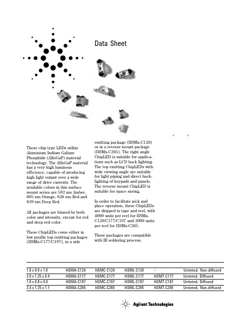
Agilent H SMx-C120/C177/C197/C265High Performance Chip LEDsData SheetFeatures•High brightness AlInGaP material •0805 or 0603 industry standard footprint with 0.4 mm height for top emitting packages•Also available in right angle emitting and reverse mounting packages•Diffused optics•Operating temperature range of –30°C to +85°C•Compatible with IR soldering •Available in 4 colors•Available in 8 mm tape on 7"diameter reel•Reel sealed in zip locked moisture barrier bags Applications•Membrane switch indicator •LCD backlighting•Push button backlighting •Front panel indicator •Symbol backlighting •Keypad backlighting •Microdisplays•Small message panel signageDescriptionThese chip type LEDs utilize Aluminium Indium Galium Phosphide (AlInGaP) material technology. The AlInGaP material has a very high luminousefficiency, capable of producing high light output over a wide range of drive currents. The available colors in this surface mount series are 592 nm Amber,605 nm Orange, 626 nm Red and 639 nm Deep Red.All packages are binned by both color and intensity, except for red and deep red color.These ChipLEDs come either in low profile top emitting packages (HSMx-C177/C197), in a sideemitting package (HSMx-C120)or in a reverse mount package (HSMx-C265). The right angle ChipLED is suitable for applica-tions such as LCD back lighting.The top emitting ChipLEDs with wide viewing angle are suitable for light piping and direct back-lighting of keypads and panels.The reverse mount ChipLED is suitable for space saving.In order to facilitate pick and place operation, these ChipLEDs are shipped in tape and reel, with 4000 units per reel for HSMx-C120/C177/C197 and 3000 units per reel for HSMx-C265.These packages are compatible with IR soldering process.Device Selection GuideDimensions (mm)[1,2]Amber RedOrange Deep Red Package Description 1.6 x 0.6 x 1.0HSMA-C120HSMC-C120HSML-C120–Untinted, Non-diffused 2.0 x 1.25 x 0.4HSMA-C177HSMC-C177HSML-C177HSMT-C177Untinted, Diffused 1.6 x 0.8 x 0.4HSMA-C197HSMC-C197HSML-C197HSMT-C197Untinted, Diffused 3.4 x 1.25 x 1.1HSMA-C265HSMC-C265HSML-C265HSMT-C265Untinted, Non-diffusedPackage DimensionsPOLARITYTERMINAL0.40 ± 0.15HSMx-C177POLARITY0.30 ± 0.15TERMINALHSMx-C1970.50 ± 0.15POLARITY0.50 ± 0.15TERMINALHSMx-C265POLARITYTERMINALHSMx-C120NOTES:1. ALL DIMENSIONS IN MILLIMETERS (INCHES).2. TOLERANCE IS ± 0.1 mm (± 0.004 IN.) UNLESS OTHERWISE SPECIFIED.Absolute Maximum Ratings at T A = 25˚CParameter HSMx-Cxxx UnitsDC Forward Current [1]25mAPeak Pulsing Current[2]100mAPower Dissipation60mWReverse Voltage (I R = 100 µA)5VLED Junction Temperature95˚COperating Temperature Range–30 to +85˚CStorage Temperature Range–40 to +85˚CSoldering Temperature See reflow soldering profile (Figures 8 & 9)Notes:1. Derate linearly as shown in Figure 4.2. Pulse condition of 1/10 duty and 0.1 ms width.Electrical Characteristics at T A = 25˚CForward Voltage Reverse Breakdown Capacitance C ThermalV F (Volts)V R (Volts)(pF), V F = 0,Resistance@ I F = 20 mA@ I R = 100 µA f = 1 MHz RθJ–PIN(˚C/W) Part Number Typ.Max.Min.Typ.Typ.HSMA-C120 1.9 2.4511400HSMA-C177/197 1.9 2.4511300HSMA-C265 1.9 2.4511550HSMC-C120 1.9 2.4515400HSMC-C177/197 1.9 2.4515300HSMC-C265 1.9 2.4515550HSML-C120 1.9 2.4520400HSML-C177/197 1.9 2.4520300HSML-C265 1.9 2.4520550HSMT-C177/197 1.9 2.4515300HSMT-C265 1.9 2.4515550V F Tolerance: ± 0.1 VOptical Characteristics at T A = 25˚CLuminous Color,Viewing LuminousIntensity Peak Dominant Angle EfficacyI V (mcd)Wavelength Wavelength 2 θ1/2ηV@ 20 mA[1]λpeak (nm)λd[2](nm)Degrees[3](lm/w) Part Number Color Min.Typ.Typ.Typ.Typ.Typ. HSMA-C120Amber28.590595592155480 HSMA-C177/197Amber28.590595592130480 HSMA-C265Amber28.575595592150480 HSMC-C120Red28.590637626155155 HSMC-C177/197Red28.590637626130155 HSMC-C265Red28.575637626150155HSML-C120Orange28.590609605155370HSML-C177/197Orange28.590609605130370HSML-C265Orange28.575609605150370 HSMT-C177/197Deep Red11.23066063913070HSMT-C265Deep Red11.22566063915070Notes:1.The luminous intensity, I V, is measured at the peak of the spatial radiation pattern which may not be aligned with the mechanical axis of the lamp package.2.The dominant wavelength, λd, is derived from the CIE Chromaticity Diagram and represents the perceived color of the device.3.θ1/2 is the off-axis angle where the luminous intensity is 1/2 the peak intensity.Light Intensity (Iv) Bin Limits [1]Intensity (mcd)Bin ID Min.Max.A 0.110.18B 0.180.29C 0.290.45D 0.450.72E 0.72 1.10F 1.10 1.80G 1.80 2.80H 2.80 4.50J 4.507.20K 7.2011.20L 11.2018.00M 18.0028.50N 28.5045.00P 45.0071.50Q 71.50112.50R 112.50180.00S 180.00285.00T 285.00450.00U 450.00715.00V 715.001125.00W 1125.001800.00X 1800.002850.00Y 2850.004500.00Note:1.Bin categories are established for classifica-tion of products. Products may not be avail-able in all categories. Please contact your Agilent representative for information on currently available bins.Amber Color Bins [1]Dom. Wavelength (nm)Bin ID Min.Max.A 582.0584.5B 584.5587.0C 587.0589.5D 589.5592.0E 592.0594.5F594.5597.0Orange Color Bins [1]Dom. Wavelength (nm)Bin ID Min.Max.A 597.0600.0B 600.0603.0C 603.0606.0D 606.0609.0E 609.0612.0F612.0615.0Tolerance: ± 0.5 nmNote:1. Bin categories are established for classification of products. Products may not be available in all categories. Please contact your Agilent representative for information on currently available bins.Tolerance: ± 1 nmTolerance: ± 15%Color Bin LimitsFigure 4. Maximum forward current vs.ambient temperature.Figure 3. Luminous intensity vs. forward current.I F – FORWARD CURRENT – mA00.41.0L U M I N O U S I N T E N S I T Y (N O R M A L I Z E D A T 20 m A )0.60.20.81.41.2Figure 2. Forward current vs. forward voltage.Figure 1. Relative intensity vs. wavelength.WAVELENGTH – nmR E L A T I V E I N T E N S I T Y – %500550600650700100101V F – FORWARD VOLTAGE – VI F – F O R W A R D C U R R E N T – m AI F M A X – M A X I M U M F O R W A R D C U R R E N T – m AT A – AMBIENT TEMPERATURE – °CFigure 5. Relative intensity vs. angle for HSMx-C120.100908070605040302010R E L A T I V E I N T E N S I T Y-90-80-70-60-50-40-30-20-100102030405060708090ANGLE100908070605040302010R E L A T I V E I N T E N S I T Y-90-80-70-60-50-40-30-20-100102030405060708090ANGLEFigure 6. Relative intensity vs. angle for HSMx-C177/197.Figure 9. Recommended Pb-free reflow soldering profile.Figure 10. Recommended soldering pattern for HSMx-C177.R E L A T I V E I N T E N S I T Y – %1000ANGLE806050702010304090-70-50-3002030507090-90-20-80-60-40-1010406080(0.035)0.8 (0.028)BOARDFigure 11. Recommended soldering pattern for HSMx-C197.Figure 7. Relative intensity vs. angle for HSMx-C265.R E L A T I V E I N T E N S I T Y – %1000ANGLE806050702010304090-70-50-3002030507090-90-20-80-60-40-1010406080NOTE:1. ALL DIMENSIONS IN MILLIMETERS (INCHES).TIMET E M P E R A T U R E* THE TIME FROM 25 °C TO PEAK TEMPERATURE = 6 MINUTES MAX.Figure 8. Recommended reflow soldering profile.T E M P E R A T U R EFigure 14. Reeling orientation.Figure 15. Reel dimensions.Figure 12. Recommended soldering pattern for HSMx-C120.Figure 13. Recommended soldering pattern for HSMx-C265.(0.031)(0.031)(0.047)Ø 20.20 MIN. (Ø 0.795 MIN.)Ø 13.1 ± 0.5 NOTE:1. ALL DIMENSIONS IN MILLIMETERS (INCHES).Figure 16. Tape dimensions.TABLE 1DIMENSIONS IN MILLIMETERS (INCHES)DIM. A ± 0.10 (0.004)DIM. B ± 0.10 (0.004)PART NUMBER DIM. C ± 0.10 (0.004)HSMx-C120 SERIES HSMx-C177 SERIES HSMx-C197 SERIES(0.020 ± 0.002)0.80 (0.031) 0.60 (0.024) 0.60 (0.024)1.90 (0.075)2.30 (0.091) 1.80 (0.071) 1.15 (0.045) 1.40 (0.055) 0.95 (0.037)NOTES:1. ALL DIMENSIONS IN MILLIMETERS (INCHES).2. TOLERANCE IS ± 0.1 mm (± 0.004 IN.) UNLESS OTHERWISE SPECIFIED.HSMx-C265 SERIES 3.70 (0.146) 1.45 (0.057) 1.30 (0.051)TABLE 1DIMENSIONS IN MILLIMETERS (INCHES)DIM. A ± 0.10 (0.004)DIM. B ± 0.10 (0.004)PART NUMBERDIM. C ± 0.10 (0.004)/semiconductorsFor product information and a complete list of distributors, please go to our web site.For technical assistance call:Americas/Canada: +1 (800) 235-0312 or (916) 788-6763Europe: +49 (0) 6441 92460China: 10800 650 0017Hong Kong: (+65) 6756 2394India, Australia, New Zealand: (+65) 6755 1939Japan: (+81 3) 3335-8152(Domestic/Interna-tional), or 0120-61-1280(Domestic Only)Korea: (+65) 6755 1989Singapore, Malaysia, Vietnam, Thailand,Philippines, Indonesia: (+65) 6755 2044Taiwan: (+65) 6755 1843Data subject to change.Copyright © 2004 Agilent Technologies, Inc.Obsoletes 5988-5501EN April 22, 20045989-0551ENConvective IR Reflow Soldering For more information on IR reflow soldering, refer toApplication Note 1060, Surface Mounting SMT LED Indicator Components .Storage Condition:5 to 30°C @ 60% RH max.Baking is required under the condition:a) the blue silica gel indicator becoming white/transparent colorb) the pack has been open for more than 1 weekBaking recommended condition:60 ± 5°C for 20 hours.Figure 17. Tape leader and trailer dimensions.END STARTSEALED WITH COVER TAPE.SEALED WITH COVER TAPE.OF CARRIER AND/ORCOVER TAPE.。
QX7136_400maLED恒流驱动
8 -0.3~VDD+0.3 500 0.5 -20~85 -40~165 2000
V V mA W
o
电流 功率消耗 温度
ILEDmax PSOT-89-5 Tmin-max Tstorage
C C
o
抗静电能力
VES型 最大 单 位 t mA V mV % mA/V
QX Micro Devices Co., Ltd. 泉芯电子技木有限公司
7 of 7
Preliminary
QX7136
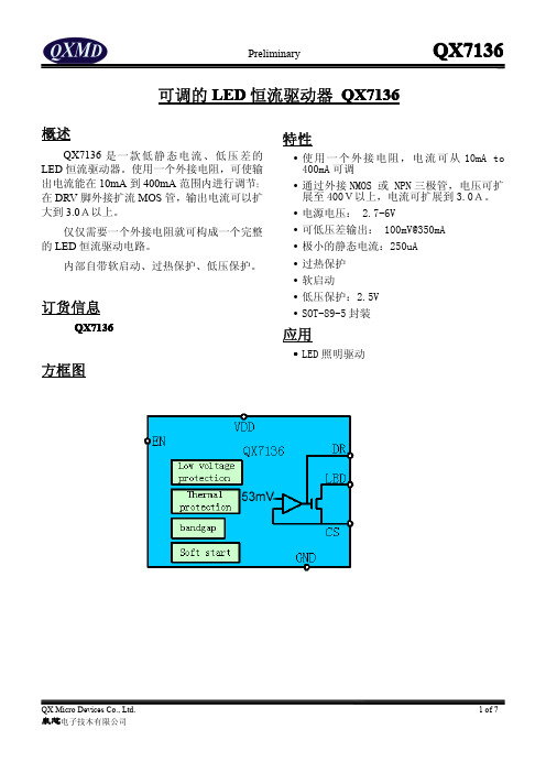
可调的 LED 恒流驱动器 QX7136
概述
QX7136 是 一 款 低 静 态 电 流 、 低 压 差 的 LED 恒流驱动器。使用一个外接电阻,可使输 出电流能在 10mA 到 400mA 范围内进行调节; 在 DRV 脚外接扩流 MOS 管,输出电流可以扩 大到 3.0A以上。 仅仅需要一个外接电阻就可构成一个完整 的 LED 恒流驱动电路。 内部自带软启动、过热保护、低压保护。
管脚名称 CS GND VDD DRV LED
描述 输出电流检测 电源地 电源 外部 MOS 驱动脚 LED 阴极输入脚
管脚功能描述:
( 1 ) C S 脚 : 此 脚 用 于 设 定 输 出 电 流 , 在 使 用 外 接 MOS 管 扩 流 扩 压 时 , 在 MOS 管 的 源 极 接 一 个 电 流 设 定 电 阻 Rcs 到 地 , 在 MOS 管 的 源 极 和 电 阻 Rcs 连 接 处 接 到 此 脚 。 CS 内 部 设 定 基 准 电 压 是 53 毫 伏 , 输 出 的 电 流 就 可 以 由 下 式 算 出 : I out=53mV/Rcs 只 要 选 定 Rcs 的 值 , 就 可 以 确 定 输 出 的 电 流 。 (2)GND脚:电源地,接至电源的负极。 ( 3 ) V D D 脚 : 内 部 电 路 供 电 脚 , 当 电 源 在 2.7V~6.0V 时 , 可 以 直 接 接 到 电 源 的 正 极 , 当 高 压 应 用 时 , 把 电 源 降 至 5.1V , 再 接 入 此 脚 给 IC 供 电 , 一 般 采 用 稳 压 二 极 管 给 IC 供 电 , 也 可 使 用 其 他 方 法 给 IC 供 电 , 但 有 保 证 VDD 脚 有 稳 定的电源供给。 ( 4 ) D R V 脚 : 当 不 用 外 接 MOS 管 扩 流 扩 压 时 , 此 脚 悬 空 ; 当 使 用 外 部 MOS 管 扩 流 扩 压 时 , 此 脚 接 外 部 MOS 管 的 门 极 。 DRV 脚 给 外 部 的 MOS 管 提 供 门 极 的 驱 动控制信号。 (5) L E D 脚 : 当 不 用 外 接 MOS 管 扩 流 扩 压 时 , 此 脚 接 LED 的 阴 极 ; 当 使 用 外 部 MOS 管 扩 流 扩 压 时 , 此 脚 悬 空 。
MAX25611高电压高亮度LED控制器评估套件说明书

MAX25611EVKIT#Evaluates: MAX25611A/MAX25611B MAX25611 Evaluation KitGeneral DescriptionThe MAX25611 evaluation kit (EV kit) provides a proven design to evaluate the MAX25611A/MAX25611B auto-motive high-voltage, high-brightness LED (HB LED) controller. The EV kit is set up for boost and buck-boost configurations and operates from a 6V to 18V DC supply voltage. The EV kit is configured to deliver up to 0.88A to one string of LEDs. The total voltage of the string can vary from 3V to 36V. The anode of the LED string should be connected to the LED+ terminal. The cathode of the LED string can be connected either to GND (boost mode) or IN (buck-boost mode). In the case of boost mode, the input voltage should not exceed the LED string voltage. Benefits and Features●Configured for Boost and Buck-Boost Application●Analog Dimming Control●Proven PCB Layout●Fully Assembled and Tested FeatureOrdering Information appears at end of data sheet.Quick StartRequired Equipment●MAX25611 EV kit●12V, 5A DC power supply● A series-connected LED string rated at least 1A●Oscilloscope with a current probeProcedureThe EV kit is fully assembled and tested. Follow the steps below to verify board operation. Caution: Do not turn on power supply until all connections are made.1)Verify that all jumpers (J1, J2, and J7) are in theirdefault positions, as shown in Table 1.2)Connect the positive terminal of the 12V supply to theVIN PCB pad and the negative terminal to the nearest GND PCB pad.3)Connect the LED string across the LED+ and LED-PCB pads on the EV kit for buck-boost configura-tion. For boost configuration, connect the LED string across the LED+ and GND PCB pads on the EV kit.The LED string voltage should be higher than the input voltage in this configuration.4)Clip the current probe on the wire connected to theLED string.5)Turn on the DC power supply.6)Verify that the LEDs turn on.7)Verify that the oscilloscope displays approximately0.88A.Click here for production status of specific part numbers.Evaluates: MAX25611A/MAX25611BMAX25611 Evaluation Kit Detailed DescriptionThe MAX25611 EV kit provides a proven design to evalu-ate the MAX25611A/MAX25611B high-voltage HB LED driver with integrated high-side current sense. The EV kit is set up for boost and buck-boost configurations and operates from a 6V to 18V DC supply voltage. The string-forward voltage can vary from 3V to 36V. The EV kit is optimized for 0.8A and a series of 8 LEDs in a string. Other configurations may require changes to component values.Analog Dimming Control (REFI)When J2 is installed across pins 1-2, the LED current is set at the maximum current. The REFI pin is connected to VCC and in this case, the LED current is given by the following equation:LED 220mVI R14=In the case of the EV kit, I LED is set to 0.88A.When J2 is installed across pins 2-3, the REFI pin is con -nected to the voltage-divider of R1 and R2, which sets the REFI voltage. If V REFI < 1.2V, then V REFI sets the LED current level.()REFI LEDV 0.2V I 5R14−=×Alternatively, the analog dimming can be controlled by removing the shunt on J2 and applying a voltage between 0 and 5.5V on the REFI test point on the EV kit. REFI voltages above 1.3V are limited to an equivalent of 1.3V inside the IC.Pulse-Dimming Input (PWMDIM)The EV kit demonstrates the PWM dimming feature of the buck controller using either an external PWM signal, or a DC voltage at the DIM pin.Analog-to-PWM dimming: Install a shunt across J1 (1-2). Adjust the potentiometer R18 to set a DC voltage on the PWMDIM pin. The PWM dimming duty cycle is set by the voltage at PWMDIM between 0.2V (0% duty) and 3V (100% duty). Alternatively, drive the PWMDIM testpoint with an external DC source. PWMDIM voltages above 3V set the dimming duty cycle to 100%.Direct PWM dimming: Leave J1 open and connect a PWM signal to the PWMDIM testpoint. Vary the duty cycle to increase or decrease the intensity of the HB LED string. The PWMDIM input of the device has a 2V (max) rising threshold and a 0.8V (min) falling threshold and is com -patible with 3.3V and 5V logic-level signals. Uninstall C2 to achieve fast PWMDIM rise and fall edges at the IC pin.Table 1. MAX25611 EV Kit Jumper DescriptionsJUMPERSHUNTPOSITION DESCRIPTIONJ11-2*Connects the PWMDIM pin of the device to VCC through a voltage divider formed by R13 and R18. The dimming duty cycle is adjusted from 0% to 100% for PWMDIM level between 0.2V and 3V. The dimming frequency is internally set at 200Hz.2-3Connects the PWMDIM pin to ground to disable the analog dimming function and keep the IC off.OpenConnect an external function generator to drive the PWMDIM pin with a signal from 0 to 3.3V or higher. PWMDIM pulse width should be at least above one switching period.Recommended PWMDIM frequency range is from 200Hz to 2kHz for visible LEDs. IR LEDs can operate at lower frequencies where flicker is not visible.J21-2*Connects VCC to the REFI pin. LED current is at the maximum value of 0.88A in this configuration.2-3Connects the REFI pin of the device to VCC through a voltage divider formed by R1 and R2.Adjusting R2 allows programming the LED current from 0 to 0.88A for REFI levels from 0.2V to 1.3V. For REFI voltages above 1.3V, the LED current is limited at 0.88A.OpenConnect an external voltage source to set the LED current from 0 to 0.88A for REFI levels from 0.2V to 1.3V. For REFI voltages above 1.3V, the LED current is limited at 0.88A.J71-2*Connects the IN pin to the same input supply as the boost power stage through a 10Ω filter resistor.OpenConnect an external supply voltage greater than 4.7V to J7 pin 2 to bias the IC IN pin.Evaluates: MAX25611A/MAX25611B MAX25611 Evaluation Kit2.2MHz OperationThe EV kit can be used to evaluate 2.2MHz operation. To test the 2.2MHz application:●Change the IC to MAX25611B (provided).●Change L2 to 2.2µH.●Change C9 to 0.22µF. R6 remains at 50Ω.●Output capacitance can be reduced to 1x 4.7µF. Notethat short pulse widths at low frequencies benefit from having higher total output capacitance to counter leak-age currents that discharge the output voltage before the next pulse.●Change other components as required (e.g., MOSFET,FET current sense R9, LED current sense R14). High-Beam/Low-Beam ApplicationThe EV kit can be used to evaluate high-beam/low-beam switching applications. Connect the low-beam LED string across LED+ and HB_LED+, and the high-beam LED string across HB_LED+ and GND. Use a function genera-tor or a DC source to drive the HIGHBEAM_OFF pad to 5V or GND to disabled or enable the high-beam LEDs. Slew rate control of the driving signal, or adjustment of R19 and C17 values can be used to control the transi-tion of the Q3 shunting FET to minimize surge currents through the low-beam LEDs.Latch CircuitThe latch circuit proves HB+LED+ short-to-battery protec-tion by disabling the shunt FET gate. This prevents the shunt FET from shorting out the battery. The latch is reset by removing power to recycle VCC.Voltage Regulator ConfigurationThe EV kit can be reconfigured as a voltage regulator using R27 and R28 as the voltage feedback resistor divider, after removing R14.()()REFIOUTV0.2R27R28V5R27−+=×Setting V REFI = 1.2V selects a large feedback signal for better accuracy and noise immunity. For simplicity, select R27 to match the programmed regulation voltage across ISENSEP and ISENSEN. For example, with V REFI = 1.2V, V(ISENSEP - ISENSEN) = 200mV, and R27 should be 200Ω. This makes 1mV per Ω or 1mA down the resis-tor string, minimizing the error due to ISENSEN leakage current. The calculation for R28 is then simplified to (VOUT - 0.2) x 1000.The following components should also be changed:●Power stage components (Q1, L2, D1, R9 and outputcapacitance) as required for the application (voltage, current rating, etc).●COMP components (R6, C9, C16) to match the appli-cation requirements.●Remove C14, R17, and Q2.#Denotes RoHS compliance.PART TYPEMAX25611EVKIT#EV KitOrdering InformationEvaluates: MAX25611A/MAX25611B MAX25611 Evaluation KitMAX25611 EV Kit Bill of MaterialsITEM REF_DES DNI/DNP QTY MFG PART #MANUFACTURER VALUE DESCRIPTION1C1, C19—2GRM32ER72A225KA35;CGA6N3X7R2A225K230;CC1210KKX7R0BB225MURATA;TDK;YAGEO2.2UFCAPACITOR; SMT (1210); CERAMIC CHIP; 2.2UF; 100V; TOL = 10%;MODEL = GRM SERIES; TG = -55°C to +125°C; TC = X7R2C2, C16—2CGA3EANP02A103J080AC TDK0.01UF CAPACITOR; SMT (0603); CERAMIC CHIP; 0.01UF; 100V; TOL = 5%; MODEL = MULTILAYER CERAMIC CHIP CAPACITOR; TC = NPO3C3—1EEE-TG2A220UP PANASONIC22UF CAPACITOR; SMT (CASE_F); ALUMINUM-ELECTROLYTIC; 22UF; 100V; TOL = 20%; MODEL = TG SERIES; TG = -40°C TO +125°C4C4, C5,C11-C13, C15—6CGA6M3X7S2A475K200AE;CGA6M3X7S2A475K200ABTDK;TDK 4.7UFCAPACITOR; SMT (1210); CERAMIC CHIP; 4.7UF; 100V;TOL = 10%; TG = -55°C TO +125°C; TC = X7S; AUTO5C6—1C1608X6S1A475K TDK 4.7UF CAPACITOR; SMT (0603); CERAMIC CHIP; 4.7UF; 10V; TOL = 10%; TG = -55°C TO +105°C; TC = X6S6C7, C8—2GCJ188R71H104KA12;GCM188R71H104K;CGA3E2X7R1H104K080AAMURATA;MURATA;TDK0.1UFCAPACITOR; SMT (0603); CERAMIC CHIP; 0.1UF; 50V;TOL = 10%; TG = -55°C TO +125°C; TC = X7R; AUTO7C9—1GCM188R71C105KA64;CGA3E1X7R1C105K080ACMURATA;TDK1UFCAPACITOR; SMT (0603); CERAMIC CHIP; 1UF; 16V; TOL = 10%;TG = -55°C TO +125°C; TC = X7R; AUTO8C10—1GRM1885C1H102JA01;C1608C0G1H102J080MURATA;TDK1000PFCAPACITOR; SMT (0603); CERAMIC CHIP; 1000PF; 50V;TOL = 5%; TG = -55°C TO +125°C9C14—1C0603C101K1GAC KEMET100PF CAPACITOR; SMT (0603); CERAMIC CHIP; 100PF; 100V; TOL = 10%; MODEL = C0G; TG = -55°C TO +125°C; TC = +10C17—1C0603X472J1GAC KEMET4700PF CAPACITOR; SMT (0603); CERAMIC CHIP; 4700PF; 100V; TOL = 5%; MODEL = FT-CAP; TG = -55°C TO +125°C; TC = C0G11C20—1C0805C104J1RAC KEMET0.1UF CAP; SMT (0805); 0.1UF; 5%; 100V; X7R; CERAMIC CHIP12C21—1CGA3E3X7S2A104K080AB TDK0.1UF CAPACITOR; SMT (0603); CERAMIC CHIP; 0.1UF; 100V; TOL = 10%; TG = -55°C TO +125°C; TC = X7S13D1—1DFLS2100DIODESINCORPORATEDDFLS2100DIODE; SCH; SMT (POWERDI-123); PIV = 100V; IF = 2A14D2—11N4148WS-7-FDIODESINCORPORATED1N4148WS-7-F DIODE; SWT; SMT (SOD-323); PIV = 75V; IF = 0.3A15D5—11N4148W-7-FDIODESINCORPORATED1N4148W-7-FDIODE; SWT; SMT (SOD-123); PIV = 100V;IF = 0.3A; -65°C TO +150°C16FB1—1HF70ACB322513TDK52INDUCTOR; SMT (1210); FERRITE-BEAD; 52; TOL = ±25%; 0.4A; -40°C TO +125°C17GND, HB_LED+,HIGHBEAM_OFF, J3-J6,LED+, LED-, VCC, VIN—119020 BUSS WEICO WIRE MAXIMPADEVK KIT PARTS; MAXIM PAD; WIRE; NATURAL; SOLID;WEICO WIRE; SOFT DRAWN BUS TYPE-S; 20AWG18J1, J2—2PCC03SAAN SULLINS PCC03SAAN CONNECTOR; MALE; THROUGH HOLE; BREAKAWAY; STRAIGHT THROUGH; 3PINS; -65°C TO +125°C19J7—1PCC02SAAN SULLINS PCC02SAAN CONNECTOR; MALE; THROUGH HOLE; BREAKAWAY; STRAIGHT THROUGH; 2PINS; -65°C TO +125°C20L1—1MSS1278T-472ML COILCRAFT 4.7UH INDUCTOR; SMT; FERRITE BOBBIN CORE; 4.7UH; TOL = ±0.2; 6.2A; -40°C TO +125°C21L2—1MSS1278T-153ML COILCRAFT15UH INDUCTOR; SMT; FERRITE; 15UH; 20%; 4.9A22MH1-MH4—49032KEYSTONE9032MACHINE FABRICATED; ROUND-THRU HOLE SPACER; NO THREAD; M3.5; 5/8IN; NYLON23Q1—1SQJA86EP-T1_GE3VISHAY SILICONIX SQJA86EP-T1_GE3TRAN; NCH; SO-8L; PD-(48W); I-(30A); V-(80V)24Q2—1FDC3535FAIRCHILDSEMICONDUCTORFDC3535TRAN; P-CHANNEL POWER TRENCH MOSFET; PCH;SSOT-6; PD-(1.6W); I-(-2.1A); V-(-80V)Evaluates: MAX25611A/MAX25611B MAX25611 Evaluation KitMAX25611 EV Kit Bill of Materials (continued)ITEM REF_DES DNI/DNP QTY MFG PART #MANUFACTURER VALUE DESCRIPTION25Q3—1FDC3512ON SEMICONDUCTOR FDC3512TRAN; N-CHANNEL POWERTRENCH MOSFET; NCH; SUPERSOT-6; PD-(1.6W); I-(3A); V-(80V)26Q4—1MMBT2907AFAIRCHILDSEMICONDUCTORMMBT2907ATRAN; SMALL SIGNAL TRANSISTOR; PNP; SOT-23;PD-(0.35W); IC-(-0.6A); VCEO-(-60V)27Q5—1MMBT2222LT1G ON SEMICONDUCTOR MMBT2222LT1G TRAN; NPN; SOT-23; PD-(0.225W); I-(0.6A); V-(30V)28R1—1CRCW060324K9FK VISHAY DALE24.9K RESISTOR; 0603; 24.9KΩ; 1%; 100PPM; 0.10W; THICK FILM29R2, R18—23296W-1-103LF BOURNS10K RESISTOR; THROUGH-HOLE-RADIAL LEAD; 3296 SERIES;10KΩ; 10%; 100PPM; 0.5W; SQUARE TRIMMING POTENTIOMETER;25 TURNS; MOLDER CERAMIC OVER METAL FILM30R3, R4—2CRCW0603100RFK;ERJ-3EKF1000;RC0603FR-07100RLVISHAY DALE;PANASONIC100RESISTOR; 0603; 100Ω; 1%; 100PPM; 0.10W; THICK FILM31R6—1CRCW060349R9FK VISHAY DALE49.9RESISTOR; 0603; 49.9Ω; 1%; 100PPM; 0.10W; THICK FILM 32R7—1CRCW06033K32FK VISHAY DALE 3.32K RESISTOR; 0603; 3.32K; 1%; 100PPM; 0.10W; THICK FILM33R8, R12,R16, R17—4CRCW06030000ZS;MCR03EZPJ000;ERJ-3GEY0R00VISHAY DALE;ROHM;PANASONIC0RESISTOR; 0603; 0Ω; 0%; JUMPER; 0.10W; THICK FILM34R9—1ERJ-8CWFR043PANASONIC0.043RESISTOR; 1206; 0.043Ω; 1%; 75PPM; 1W; THICK FILM35R10—1CRCW0603475KFK VISHAY DALE475K RESISTOR; 0603; 475KΩ; 0.1%; 100PPM; 0.1W; THICK FILM36R11—1CRCW060310K0FK;ERJ-3EKF1002VISHAY DALE;PANASONIC10K RESISTOR; 0603; 10K; 1%; 100PPM; 0.10W; THICK FILM37R13—1CRCW06033K00FK VISHAY DALE3K RESISTOR; 0603; 3KΩ; 1%; 100PPM; 0.10W; THICK FILM 38R14—1LRC-LR2512LF-01-R250F TT ELECTRONICS0.25RESISTOR; 2512; 0.25Ω; 1%; 100PPM; 2W; THICK FILM 39R15—1CRCW06031M00JN VISHAY DALE1M RESISTOR; 0603; 1MΩ; 5%; 200PPM; 0.10W; METAL FILM 40R19—1CRCW060320K0JN VISHAY DALE20K RESISTOR; 0603; 20KΩ; 5%; 200PPM; 0.10W; METAL FILM 41R21—1ERA-V15J100V PANASONIC10RESISTOR; 0603; 10Ω; 5%; 1500PPM; 0.063W; METAL FILM 42R22—1LRC-LR1206LF-01-R100-F TT ELECTRONICS0.1RESISTOR; 1206; 0.1Ω; 1%; 100PPM; 0.5W; THICK FILM 43R23, R25—2ERJ-3GEYJ102V PANASONIC1K RESISTOR; 0603; 1KΩ; 5%; 200PPM; 0.10W; THICK FILM 44R24—1301-10K-RC XICON10K RESISTOR, 0603, 10KΩ, 5%, 200PPM, 1/16W, THICK FILM 45R26—1ERJ-3GEYJ472V PANASONIC 4.7K RESISTOR; 0603; 4.7KΩ; 5%; 200PPM; 0.10W; THICK FILM46SU1-SU3—3S1100-B;SX1100-B KYCON;KYCON SX1100-B TEST POINT; JUMPER; STR; TOTAL LENGTH = 0.24IN; BLACK; INSULATION = PBT;PHOSPHOR BRONZE CONTACT = GOLD PLATED47TP1—17006KEYSTONE7006CONNECTOR; PANELMOUNT; BINDING POST; STRAIGHT THROUGH; 1PIN; RED48TP2—17007KEYSTONE7007CONNECTOR; PANELMOUNT; BINDING POST; STRAIGHT THROUGH; 1PIN; BLACK49U1—1MAX25611ATC MAXIM MAX25611ATC EVKIT PART - IC; MAX25611ATC; PACKAGE OUTLINE DRAWING: 21-0139; LAND PATTERN DRAWING: 90-0068; TQFN16-EP50PCB—1MAX25611MAXIM PCB PCB:MAX2561151C18DNP0C0805C104J1RAC KEMET0.1UF CAP; SMT (0805); 0.1UF; 5%; 100V; X7R; CERAMIC CHIP52D3DNP01N4148W-7-FDIODESINCORPORATED1N4148W-7-FDIODE; SWT; SMT (SOD-123); PIV = 100V;IF = 0.3A; -65°C TO +150°C53R5DNP0ERJ-8CWFR043PANASONIC0.043RESISTOR; 1206; 0.043Ω; 1%; 75PPM; 1W; THICK FILM 54R20DNP0CRCW0603499KFK VISHAY DALE499K RESISTOR; 0603; 499KΩ; 1%; 100PPM; 0.1W; THICK FILM 55R27DNP0CRCW0603220RFK VISHAY DALE220RESISTOR; 0603; 220Ω; 1%; 100PPM; 0.10W; THICK FILM 56R28DNP0CRCW060360K4FK VISHAY DALE60.4K RESISTOR, 0603, 60.4KΩ, 1%, 100PPM, 0.1W, THICK FILM80TOTALEvaluates: MAX25611A/MAX25611B MAX25611 Evaluation KitMAX25611 EV Kit SchematicsEvaluates: MAX25611A/MAX25611BMAX25611 Evaluation Kit MAX25611 EV Kit Component Placement Guide—Top SilkscreenMAX25611 EV Kit PCB Layout DiagramsEvaluates: MAX25611A/MAX25611BMAX25611 Evaluation Kit MAX25611 EV Kit PCB Layout—Top ViewMAX25611 EV Kit PCB Layout Diagrams (continued)Evaluates: MAX25611A/MAX25611BMAX25611 Evaluation Kit MAX25611 EV Kit PCB Layout—Bottom ViewMAX25611 EV Kit PCB Layout Diagrams (continued)Maxim Integrated │ MAX25611 EV Kit Component Placement Guide—Bottom SilkscreenMAX25611 EV Kit PCB Layout Diagrams (continued)Maxim Integrated cannot assume responsibility for use of any circuitry other than circuitry entirely embodied in a Maxim Integrated product. No circuit patent licenses are implied. Maxim Integrated reserves the right to change the circuitry and specifications without notice at any time.Maxim Integrated and the Maxim Integrated logo are trademarks of Maxim Integrated Products, Inc.© 2019 Maxim Integrated Products, Inc. │ 11REVISIONNUMBERREVISION DATE DESCRIPTION PAGES CHANGED 03/19Initial release —13/19Updated part number to MAX25611A/MAX25611B 1–11Revision HistoryFor pricing, delivery, and ordering information, please visit Maxim Integrated’s online storefront at https:///en/storefront/storefront.html .MAX25611EVKIT#。
QX7136中文版规格书
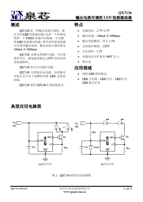
典型应用电路图DCR CS1V IN (a)低压应用V IN (b)高压应用图1:QX7136典型应用电路图概述QX7136是一种输出电流可调的、低压差的LED 恒流驱动器,仅需一个外接电阻和一个NMOS 管就可以构成一个完整的LED 恒流驱动电路,调节该外接电阻就可以调节输出电流,输出电流可调范围为100mA 到3000mA 。
QX7136内置过热保护功能,可有效保护芯片,避免温度超过120oC 时因过热而造成损坏。
QX7136具有欠压保护功能。
QX7136自带软启动功能,该功能可以防止芯片在上电瞬间出现LED 亮度的闪烁。
QX7136采用SOT-89-5的封装形式。
特点电源电压:2.7V~5.5V输出电流:100mA 到3000mA 。
输出电流精度:优于±5% 过热保护阈值:120o C欠压保护:2.5V电源电压可扩展至400V 以上。
软启动 应用领域线性LED 照明驱动LED 手电筒、LED 台灯、LED 矿灯、LED 指示灯等订货信息产品型号QX7136丝印7136XXXX批号年份封装及管脚分配SOT-89-57136 XXXX13254CSGND VDDDRV NC管脚定义内部电路方框图VDDCSDRVGND图2:QX7136的内部电路方框图极限参数(注1)注1:超过上表中规定的极限参数会导致器件永久性损坏。
而工作在以上极限条件下可能会影响器件的可靠性。
电特性除非特别说明,V IN =5V,T A =25o C电特性(接上一页)除非特别说明,V IN =5V , T A =25o C典型曲线除非特别说明,V IN =5V ,T A =25o C ,NMOS 管型号为AP2306。
应用指南工作原理QX7136是一种低静态电流、低压差的LED线性降压恒流驱动器。
通过采样输出电流作为负反馈来形成整个工作环路的稳定工作。
QX7136采用5.0V工艺制作,正常工作电压为3.0V到5.5V,当电源电压高过5.5V时通过外部的钳位电路使芯片工作电压钳位在5.5V即可满足高压大电流恒流LED驱动。
IAR编译错误
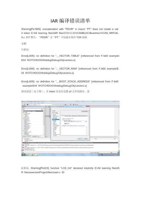
IAR编译错误清单Warning[Pe1665]: concatenation with "PDOR" in macro "PT" does not create a valid token E:\All learning files\IAR files\四轴\电调\VCANBLDC\Board\src\VCAN_NRF24L0.c 317警告:“PDDR”宏“PT”不创建有效的TOK级联未解1,错误:Error[Li005]: no definition for "__VECTOR_TABLE" [referenced from F:\k60 example\ E04 WOTCHDOG\Watdog\Debug\Obj\vectors.o]Error[Li005]: no definition for "__VECTOR_RAM" [referenced from F:\k60 example\E 04 WOTCHDOG\Watdog\Debug\Obj\vectors.o]Error[Li005]: no definition for "__BOOT_STACK_ADDRESS" [referenced from F:\k60 example\E04 WOTCHDOG\Watdog\Debug\Obj\vectors.o]错误原因(见下图):在linker里没有设置icf文件的路径。
说2,错误:Warning[Pe223]: function "LCD_Init" declared implicitly D:\All learning files\IA R files\exercise\Project\files\main.c 30files\exercise\Project\files\main.c 31Warning[Pe223]: function "LCD_P8x16Str" declared implicitly D:\All learning files\IAR files\exercise\Project\files\main.c 40Warning[Pe223]: function "LCD_P6x8Str" declared implicitly D:\All learning files\IAR f iles\exercise\Project\files\main.c 41Warning[Pe223]: function "LCD_CLS" declared implicitly D:\All learning files\IAR files\ exercise\Project\files\main.c 44Error[Pe020]: identifier "longqiu96x64" is undefined D:\All learning files\IAR files\exer cise\Project\files\main.c 45或者:Error[Pe101]: "uint8" has already been declared in the current scope (at line 72 of "D:\All learning files\IAR files\exercise\ D:\All learning files\IAR files\exercise\LI B\drivers\LQ12864\LQ12864.h 10Project\iar\..\..\LIB\cpu\arm_cm4.h")Error[Pe070]: incomplete type is not allowed D:\All learning files\IAR files\exercise\LI B\drivers\LQ12864\LQ12864.h 10Error[Pe065]: expected a ";" D:\All learning files\IAR files\exercise\LIB\drivers\LQ1286 4\LQ12864.h 10Error while running C/C++ Compilermain.cError[Pe101]: "uint8" has already been declared in the current scope (at line 72 of "D:\All learning files\IAR files\exercise\ D:\All learning files\IAR files\exercise\LIB\drive rs\LQ12864\LQ12864.h 10Project\iar\..\..\LIB\cpu\arm_cm4.h")Error[Pe070]: incomplete type is not allowed D:\All learning files\IAR files\exercise\LI B\drivers\LQ12864\LQ12864.h 10Error[Pe065]: expected a ";" D:\All learning files\IAR files\exercise\LIB\drivers\LQ1286 4\LQ12864.h 10Warning[Pe223]: function "LCD_Init" declared implicitly D:\All learning files\IAR files\e xercise\Project\files\main.c 30Warning[Pe223]: function "Draw_LibLogo" declared implicitly D:\All learning files\IAR files\exercise\Project\files\main.c 31files\exercise\Project\files\main.c 40Warning[Pe223]: function "LCD_P6x8Str" declared implicitly D:\All learning files\IAR f iles\exercise\Project\files\main.c 41Warning[Pe223]: function "LCD_CLS" declared implicitly D:\All learning files\IAR files\ exercise\Project\files\main.c 44Error[Pe020]: identifier "longqiu96x64" is undefined D:\All learning files\IAR files\exer cise\Project\files\main.c 45Error while running C/C++ Compiler注意:我这是把LQ12864.h中的void byte longqiu96x64[768];//void LCD_Init(void);//void LCD_CLS(void);//void LCD_P6x8Str(byte x,byte y,byte ch[]);//void LCD_P8x16Str(byte x,byte y,byte ch[]);//void LCD_P14x16Str(byte x,byte y,byte ch[]);void LCD_Print(byte x, byte y, byte ch[]);// void LCD_PutPixel(byte x,byte y);//void LCD_Rectangle(byte x1,byte y1,byte x2,byte y2,byte gif);//void Draw_LQLogo(void);//void Draw_LibLogo(void);看到没我都给注释了,然后出现这么多错误,最后又把本来是extern byte longqiu96x64[7 68];改成void byte longqiu96x64[768];于是出现了:Error[Pe101]: "uint8" has already been declared in the current scope (at line 72 of "D:\All learning files\IAR files\exercise\ D:\All learning files\IAR files\exercise\LIB\drive rs\LQ12864\LQ12864.h 10Project\iar\..\..\LIB\cpu\arm_cm4.h")Error[Pe070]: incomplete type is not allowed D:\All learning files\IAR files\exercise\LI B\drivers\LQ12864\LQ12864.h 10Error[Pe065]: expected a ";" D:\All learning files\IAR files\exercise\LIB\drivers\LQ1286 4\LQ12864.h 10Error while running C/C++ CompilerIAR 6.20编译错误清单1、①错误描述:Tool Internal Error:Internal Error: [CoreUtil/General]: Access violation (0xc0000005) at 007588A5 (reading from address 0x0)Internal Error: [CoreUtil/General]: Access violation (0xc0000005) at 007588A5 (reading from address 0x0)Error while running C/C++ Compiler②错误原因:High配置设置为Size,应该为Low2、①错误描述:Fatal Error[Pe1696]: cannot open source file "inc/hw_types.h" E:\StellarisWareM3_9D92\boards\dk-lm3s9b96\boot_demo2\boot_demo2.c 25②错误原因:C/C++ Complier(Assember)->Preprocessor->Additional include directories:$PROJ_DIR$\.$PROJ_DIR$\..$PROJ_DIR$\..\..\..3、①错误描述:Fatal Error[Pe1696]: cannot open source file "lwip/opt.h" E:\StellarisWareM3_9D92\utils\lwiplib.h 44②错误原因:C/C++ Complier-(Assember)>Preprocessor->Additional include directories:$PROJ_DIR$\..\..\..\third_party\lwip-1.3.2\apps$PROJ_DIR$\..\..\..\third_party\bget$PROJ_DIR$\..\..\..\third_party\lwip-1.3.2\ports\stellaris\include$PROJ_DIR$\..\..\..\third_party\lwip-1.3.2\src\include$PROJ_DIR$\..\..\..\third_party\lwip-1.3.2\src\include\ipv4$PROJ_DIR$\..\..\..\third_party\lwip-1.3.2\src\include\lwip$PROJ_DIR$\..\..\..\third_party4、①错误描述:Fatal Error[Pe035]: #error directive: Unrecognized COMPILER! E:\StellarisWareM3_9D92\boards\dk-lm3s9b96\drivers\set_pinout.h 59Error while running C/C++ Compiler②错误原因:C/C++ Complier-(Assember)>Preprocessor->Defined symbols: ewarm5、①错误描述:Error[Pe020]: identifier "ROM_pvAESTable" is undefined E:\StellarisWareM3_9D92\third_party\aes\aes.c 319②错误原因:6、①错误描述:Error[Li005]: no definition for "main" [referenced from cmain.o(rt7M_tl.a)]Error while running Linker②错误原因:定义函数:int main(void) { return (0); }7、①错误描述:Error[Li005]: no definition for "main" [referenced from cmain.o(rt7M_tl.a)]Error while running Linker②错误原因:如果是库是库函数,在:General Options->Output->Output file:选择:Library项4、①错误描述:Fatal Error[Pe1696]: cannot open source file "uip.h" E:\StellarisWareM3_9D92\third_party\uip-1.0\apps\dhcpc\dhcpc.c 37②错误原因:5、①错误描述:②错误原因:$PROJ_DIR$\..\..\..\third_party\lwip-1.3.2\apps$PROJ_DIR$\..\..\..\third_party\bget$PROJ_DIR$\..\..\..\third_party\lwip-1.3.2\ports\stellaris\include$PROJ_DIR$\..\..\..\third_party\lwip-1.3.2\src\include$PROJ_DIR$\..\..\..\third_party\lwip-1.3.2\src\include\ipv4$PROJ_DIR$\..\..\..\third_party$PROJ_DIR$\..\..\..\third_party\uip-1.0$PROJ_DIR$\..\..\..\third_party\uip-1.0\uip$PROJ_DIR$\..\..\..\third_party\uip-1.0\apps$PROJ_DIR$\..\..\..\third_party\\speex-1.2rc1\include$PROJ_DIR$\..\..\..\third_party\\speex-1.2rc1\include\speex$PROJ_DIR$\..\..\..\third_party\\speex-1.2rc1\stellaris6、①错误描述:Fatal Error[Pe035]: #error directive: You now need to define either FIXED_POINT or FLOATING_POINT E:\StellarisWareM3_9D92\third_party\speex-1.2rc1\libspeex\arch.h 65②错误原因:7、①错误描述:Fatal Error[Pe035]: #error directive: "Unrecognized/undefined driver for DISK0!" E:\StellarisWareM3_9D92\third_party\fatfs\port\dual-disk-driver.c 62Error while running C/C++ Compiler②错误原因:UART_BUFFEREDDISK0_DK_LM3S9B96DISK1_USB_MSCINCLUDE_BGET_STATS8、①错误描述:Error[Pe020]: identifier "ROM_pvAESTable" is undefined E:\SWM3_9D92(6.20)\third_party\aes\aes.c 359Error while running C/C++ Compiler②错误原因:10、①错误描述:Fatal Error[Pe035]: #error directive: You now need to define either FIXED_POINT or FLOATING_POINT E:\SWM3_9D92(6.20)\third_party\speex-1.2rc1\libspeex\arch.h 65Error while running C/C++ Compiler②错误原因:11、①错误描述:Error[Li005]: no definition for "ROM_SysCtlClockSet" [referenced from E:\SWM3_9D92(6.20)\boards\dk-lm3s9b96\safertos_demo\Debug\Obj\safertos_demo.o] Error[Li005]: no definition for "ROM_FlashUserGet" [referenced from E:\SWM3_9D92(6.20)\boards\dk-lm3s9b96\safertos_demo\Debug\Obj\lwip_task.o] Error[Li005]: no definition for "ROM_IntPrioritySet" [referenced from E:\SWM3_9D92(6.20)\boards\dk-lm3s9b96\safertos_demo\Debug\Obj\lwip_task.o] Error[Li005]: no definition for "ROM_GPIOPinTypeGPIOOutput" [referenced from E:\SWM3_9D92(6.20)\boards\dk-lm3s9b96\safertos_demo\Debug\Obj\led_task.o]Error[Li005]: no definition for "ROM_GPIOPinWrite" [referenced from E:\SWM3_9D92(6.20)\boards\dk-lm3s9b96\safertos_demo\Debug\Obj\led_task.o]Error[Lp011]: section placement failed: unable to allocate space for sections/blocks with a total estimated minimum size of 0x11e54 bytes in<[0x20000000-0x2000ffff]> (total uncommitted space 0x10000).Error while running Linker②错误原因:12、①错误描述:Error[Lp011]: section placement failed: unable to allocate space for sections/blocks with a total estimated minimum size of 0x11e54 bytes in <[0x20000000-0x2000ffff]> (total uncommitted space 0x10000).Error while running Linker。
OC6700规格书2017年新版
静电耐压值(人体模型)
最大值 60 5.5
VDD+0.3 0.8 125 85 125 240 2000
单位 V V
V W oC
PP
oC
PP
oC
PP
oC
PP
V
注 1:超过上表中规定的极限参数会导致器件永久性损坏,而工作在以上极限条件下可能会影响器件的可靠性。
OC6700_V1.0
4
深圳市 惠新晨电子有限公 司
芯片通过 CS 管脚采样电感电流,实现峰值电流控制。此外,CS 脚还用来限制最大输入 电流,实现过流保护功能。
系统关断时间可通过连接到TOFF管脚的电容COFF来设置。通过设定关断时间,可设置系 统的工作频率。
COMP 管脚是误差放大器的输出端,可以在 COMP 脚外接电阻、电容来实现频率补偿。
OC6700 内部集成了 VDD 稳压管,以及软启动和过温保护电路。
深圳市 惠新晨电子有限公 司
概述
OC6700 是一款内置 60V 功率 NMOS 高效率、高精度的升压型大功率 LED 恒流 驱动芯片。
OC6700 内置高精度误差放大器,固 定关断时间控制电路,恒流驱动电路等, 特别适合大功率、多个高亮度 LED 灯串恒 流驱动。
OC6700 采用固定关断时间的控制方 式,关断时间可通过外部电容进行调节, 工作频率可根据用户要求而改变。
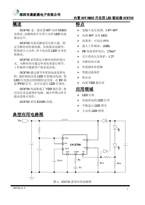
内置 60V NMOS 升压型 LED 驱动器 OC6700
管脚描述
管脚号 1 2 3 4 5 6 7 8
管脚名 GND EN COMP FB SW CS TOFF VDD
管脚类型 地 输入 输出 输入 输出 输入 输入 电源
描述 接地 芯片使能端,高电平有效 频率补偿脚 输出电流检测反馈脚 功率管漏极 输入限流检测脚 关断时间设置 芯片电源
德州仪器MAX16826评估板使用手册说明书
Evaluates: MAX16826MAX16826 Evaluation KitGeneral DescriptionThe MAX16826 evaluation kit (EV kit) provides a proven design to evaluate the MAX16826, a four-string, I 2C programmable high-brightness LED (HB LED) driver with PWM dimming control. The EV kit also includes Windows ® 2000/XP/Vista ®-compatible software that pro-vides a simple graphical user interface (GUI) for exercis-ing the features of the MAX16826. The MAX16826 EV kit PCB comes with a MAX16826ATJ+ installed. The EV kit is configured in a boost application.This EV kit can be modified by changing component val -ues on the board for other configurations (including RGB LED applications). Refer to the MAX16826 IC data sheet for more information.Features●Four Independently Controllable LED Strings ●7 LEDs Per String Configuration●Independently Programmable 50mA to 150mAString Current●7.5V to 22V Input Voltage●Can Withstand Automotive Load Dump Up to 40Vfor 400ms●0% to 100% DIM Duty Cycle Range ●Shorted LED Protection and Detection ●Open LED String Detection●Adaptive Boost-Stage Voltage Optimization●Convenient Breakaway LED Driver Board EasilyAdaptable to End Application ●Low Mechanical Profile●Windows 2000/XP/Vista (32-Bit)-Compatible Software ●USB-PC Interface●USB-to-I 2C On-Board Circuitry ●Fully Assembled and Tested ●Lead-Free and RoHS Compliant19-4271; Rev 1; 12/20Windows and Windows Vista are registered trademarks of Microsoft Corp.+Denotes lead-free and RoHS compliant.#Denotes RoHS compliant.PARAMETERDESCRIPTION Configuration 7 white LEDs/stringNumber of Strings4 strings LED Current Adjustment Range 50mA to 150mATotal Maximum LED Power 16.8W V IN (min)7.5V V IN (max)22V Load Dump40V for < 400ms Nominal Boost Voltage Adjustment Range22.4V to 32VNominal OVP Trip Threshold 35V Boost Stage Switching Frequency350kHzPARTTYPE MAX16826EVKIT+EV Kit MAX16826EVKIT#EV KitDESIGNATION QTY DESCRIPTIONC1, C2, C3, C5–C8, C12, C15,C17, C23, C2412100nF ±10%, 16V X7R ceramic capacitors (0603)TDK C1608X7R1C104K C9133nF ±10%, 50V X7R ceramic capacitor (0603)TDK C1608X7R1H333K C10, C11222pF ±5%, 50V C0G ceramic capacitors (0603)TDK C1608C0G1H220J C13, C14,C18–C2161μF ±10%, 16V X7R ceramic capacitors (0603)TDK C1608X7R1C105K C16, C25210μF ±10%, 10V X5R ceramic capacitors (1210)Murata GRM32FR61A106KDESIGNATION QTY DESCRIPTIONC26, C28210μF ±20%, 50V X5R ceramic capacitors (2220)Murata GRM55DR61H106K C27110μF ±20%, 50V X7S ceramic capacitor (1210)Taiyo Yuden UMK325BJ106MM-T C2912.2nF ±5%, 50V C0G ceramic capacitor (0603)Murata GRM1885C1H222K C3011μF ±10%, 50V X7R ceramic capacitor (1210)Murata GRM32RR71H105K C3214.7μF ±10%, 6.3V X5R ceramic capacitor (0603)Murata GRM188R60J475KLED Driver Board SpecificationOrdering InformationComponent ListClick here to ask about the production status of specific part numbers.DESIGNATION QTY DESCRIPTIONC3312200pF ±10%, 50V X7R ceramic capacitor (0402)Murata GRM155R71H222KC34, C35247μF ±20%, 50V electrolytic capacitorsPanasonic EEE-FK1H470XPC36, C370Not installed, capacitors (0603)C3811000pF ±5%, 50V C0G ceramic capacitor (0402)Murata GRM1555C1H102JA01DC391220pF ±5%, 50V C0G ceramic capacitor (0402)Murata GRM1555C1H221JC401100pF ±5%, 50V C0G ceramic capacitor (0402)Murata GRM1555C1H101JC41–C4440.01μF ±10%, 50V X7R ceramic capacitors (0402)Murata GRM155R71H103KC450Not installed, capacitor (0402)D1160V, 1A Schottky diode (SMB) Diodes, Inc. B160B-13-FJ11USB series-B right-angle PC-mount receptacleJ2, J30Not installed JU2–JU873-pin headersL11Ferrite bead (0603) TDK MMZ1608R301AL2122μH ±20%, 5A, 52mΩ inductor Coilcraft MSS1260-223MlLED11Red LED (0603) Panasonic LNJ208R8ARAP1, P22Connectors, FFC/FPC 18-pos, 1mm P31Connector, FFC/FPC 6-pos, 1mmQ1140V, 9A, 2.5W n-channel MOSFET (8 SO)International Rectifier IRF7469Q2–Q5455V, 1.9A, 160mΩ n-channel MOSFET s (SOT223) International Rectifier IRFL014NPbFR11220Ω ±5% resistor (0603)R21 2.2kΩ ±5% resistor (0603)R3, R9, R103 1.5kΩ ±5% resistors (0603) R4, R5227Ω ±5% resistors (0603)R61470Ω ±5% resistor (0603)R71100kΩ ±5% resistor (0603)R817.5kΩ ±1% resistor (0603)R11168Ω ±1%, 0.25W resistor (1206)DESIGNATION QTY DESCRIPTION R1210.04Ω ±1%, 0.5W sense resistor(2010)Vishay/Dale WSL2010R0400FEA R131215kΩ ±1% resistor (0402) R14, R16210kΩ ±1% resistors (0402) R151249kΩ ±1% resistor (0402)R171 1.27kΩ ±1% resistor (0603)R181182kΩ ±1% resistor (0603)R1912kΩ ±1% resistor (0402) R20, R22,R24, R264100kΩ ±1% resistors (0402) R21, R23,R25, R27416.5kΩ ±1% resistors (0402) R28–R3142.2Ω ±1%, 100mW sense resistors(0603)Panasonic ECG ERJ-3RQF2R2V R32, R3320Ω ±5% resistors (0603)R34–R3740Ω ±5% resistors (0402)R38112.1Ω ±1% resistor (0805)R391470Ω ±5% resistor (0402)R40110kΩ ±5% resistor (0603) R41–R444237kΩ ±1% resistors (0603) U11LED driver (32 TQFN)Maxim MAX16826ATJ+ U2, U82Microcontrollers (68 QFN-EP*)Maxim MAXQ2000-RAX+ U31UART-to-USB converter (32 TQFP)FTDI FT232BLU4193C46A 3-wire EEPROM (8 SO)Atmel AT93C46A-10SU-2.7 U51p-channel MOSFET power switch(8 SO)Maxim MAX890LESA+U61LDO regulator (5 SC70)Maxim MAX8511EXK25+T U71LDO regulator (5 SC70)Maxim MAX8511EXK33+T Y1120MHz crystal oscillatorY216MHz crystalHong Kong X’talsSSL6000000E18FAF—1Cable, flat flex 18-position, 1mm, 5in—7Shunts—1USB high-speed A-to-B cable,5ft (1.5m)—1PCB: MAX16828 Evaluation Kit+Component List (continued)*Exposed pad.Quick StartRecommended EquipmentBefore beginning, the following equipment is needed: ●MAX16826 EV kit (USB cable included)● A user-supplied Windows 2000/XP/Vista PC with a spare USB port●7V to 24V, 5A DC power supply●Four strings of white LEDs (7 LEDs/string)Note: In the following sections, software-related items are identified by bolding. Text in bold refers to items directly from the EV kit software. Text in bold and underlined refers to items from the Windows operating systemProcedureThe MAX16826 EV kit is fully assembled and tested. Follow the steps below to verify board operation:1) Visit /evkitsoftware to down-load the latest version of the EV kit software,16826Rxx.ZIP (xx in the filename denotes the soft -ware version number). Save the EV kit software to a temporary folder and uncompress the ZIP file.2) Install the EV kit software on your computer by run -ning the INSTALL.EXE program inside the temporary folder. The program files are copied and icons are created in the Windows Start | Programs menu.3) Verify that all jumpers (JU2–JU8) are in their defaultpositions, as shown in Table 1.4) Connect the USB cable from the PC to the EV kitboard. A New Hardware Found window pops up when installing the USB driver for the first time. If you do not see a window that is similar to the one described above after 30 seconds, remove the USB cable from the board and reconnect it. Administra-tor privileges are required to install the USB device driver on Windows.5) Follow the directions of the Add New HardwareWizard to install the USB device driver. Choose the Search for the best driver for your device option. Specify the location of the device driver to be C:\Program Files\MAX16826 (default installation direc-tory) using the Browse button. During device driver installation, Windows may show a warning message indicating that the device driver Maxim uses does not contain a digital signature. This is not an error condi-tion and it is safe to proceed with installation. Refer to the USB_Driver_Help.PDF document included with the software for additional information.6) Set the output of the power supply to 12V. Turn offthe power supply.7) Connect the positive terminal of the power supply tothe VIN pad of the LED driver board.Note: Indicate that you are using the MAX16826 when contacting these component suppliers.SUPPLIERPHONE WEBSITECoilcraft, Diodes, Inc.Hong Kong X’tals Ltd.852-******** International RectifierMurata Electronics North America, Panasonic Taiyo Yuden TDK Vishay/Dale402-563-6866FILE DESCRIPTIONINSTALL.EXE Installs the EV kit files on your computerMAX16826.EXE Application program FTDIBUS.INF USB device driver file FTDIPORT.INF VCP device driver file UNINST.INI Uninstalls the EV kit software USB_Driver_Help.PDFUSB driver installation help fileComponent SuppliersMAX16826 EV Kit Files8) Connect the negative terminal of the power supply tothe PGND pad of the LED driver board.9) Ensure that the supplied ribbon cable is firmly con -nected to the P1 and P2 connectors.10) Connect the anode ends of the LED strings to theP3-1 pin of the P3 connector.11) Connect the cathode ends of the LED strings to theP3-2 to P3-5 pins of the P3 connector.12) Turn on the power supply13) Start the MAX16826 EV kit software by opening itsicon in the Start | Programs menu. The EV kit soft-ware main window appears, as shown in Figure 1.14) Press the Start button to start the LED driver.15) Verify that all of the LEDs are lit.Table 1. MAX16826 EV Kit Jumper Descriptions (JU2–JU8)*Default position.JUMPER SHUNT POSITIONDESCRIPTIONJU21-2*On-board PWM signal for Ch12-3Connect user-supplied PWM signal for Ch1 to the on-board DIM1 pad JU31-2*On-board PWM signal for Ch22-3Connect user-supplied PWM signal for Ch2 to the on-board DIM2 pad JU41-2*MAX16826 SDA signal connected to on-board microcontroller 2-3Connect user-supplied SDA signal to the on-board SDA pad JU51-2*MAX16826 SCL signal connected to on-board microcontroller 2-3Connect user-supplied SCL signal to the on-board SCL pad JU61-2*MAX16826 SYNC/EN signal connected to on-board microcontroller 2-3Connect user-supplied SYNC/EN signal to the on-board SYNC/EN pad JU71-2*On-board PWM signal for Ch32-3Connect user-supplied PWM signal for Ch3 to the on-board DIM3 pad JU81-2*On-board PWM signal for Ch42-3Connect user-supplied PWM signal for Ch4 to the on-board DIM4 padDetailed Description of SoftwareThe MAX16826 evaluation kit software has all the functions to evaluate the MAX16826 IC. To start the MAX16826 EV kit software, click Start | Programs | Maxim MAX16826 Evaluation Kit | Maxim MAX16826 Evaluation Kit that is created during installation. The GUI main window appears as shown in Figure 1.Figure 1. MAX16826 EV Kit Software Main WindowString Current SetThe String Current Set group box is located at the upperleft corner of the main window. Use the scrollbars toadjust the current of the LED strings. The correspondingvalues of the current will be shown in the adjacent editboxes. Press the Read button to read the values from thelinear regulator output registers of the MAX16826. Theequivalent values of the output current will be shown inthe edit boxes.Boost Output ControlThe Boost Output Control Mode group box has thefunctions to control the boost output voltage.To control the boost output voltage manually, click on theradio button next to the Manual Control group box. Usethe scrollbar to adjust the output voltage, and the volt-age value will be displayed in the adjacent edit box. Theactual boost output voltage can be seen in the Read BackValues group box.To use the software automatic control, click on the radiobutton next to the Software Control group box. The editbox next to the Set button is used to change the Drain toGND regulated voltage of the current sink FETs on the LEDstring with the highest voltage drop. This voltage setting willdepend on how much overhead the user is willing to have.If the set value is too low, the LED currents will no longerbe well regulated and may indeed drop because the boostvoltage might fall too low. The scrollbar in this mode willmove automatically to compensate and regulate the outputvoltage. The update rate is approximately once per second.In any case, the channel with the lowest voltage across thesink FET will be regulated to the value in the edit box. DIM Pulse Width Modulation (DPWM)The DPWM group box is located at the center of the mainwindow. The four DIM PWM signals generated by theon-board MAXQ2000 microcontrollers are used to controlthe brightness of the LEDs. Adjust the scrollbars in theDPWM Duty Cycle group box to change the duty cycles of the PWM signals and the values of the duty cycle (%)are shown in the adjacent edit boxes. Check the Set AllChannels to 100% Duty Cycle checkbox to force all channel duty cycles to 100%.In the DPWM Frequency group box, change the DPWMfrequency by adjusting the scrollbar position and pressthe Set button. The frequency value will be shown in theedit box.To guarantee that the leading edge of all the DIM signalsare synchronized, press the Set button in the DPWMFrequency group box.Press the Start button to start to generate the PWM signals.Press the Stop button to stop all PWM signals.StatusThe Status group box is located at the right of the main window. The software reads the external FET drain voltage measurements, and the boost output voltage measurement from the ADC output registers of the MAX16826. The software multiplies the measured values by the appropriate scaling factor and then displays them in the Read Back Values group box.Enter the values into the edit boxes in the Fault Level Set group box to set the fault-detection values. When the value in the Read Back Values group box is less than the fault-detection value, then the color of the read-back value changes to dark green. When the read-back value is 0 to 10% higher than the fault-detection value, the read-back value turns a lime color. If the read-back value is more than 10% higher than the fault-detection value, then the read-back value turns purple. The read-back value turns red when it is more than 20% higher than the fault-detection value.The software also reads the fault register to detect the fault conditions. If a fault condition exists, it will be shown in the String Fault Status group box. See Table 2 for the fault-condition explanations.Press the Read button to update the Status group box. By checking the Automatic Read checkbox, the Status group box will be automatically updated every second. Enable/DisableThe Enable/Disable group box controls the signal on the SYNC/EN pin. Click on the Enable radio button to set the signal high and enable the MAX16826. Click on the Disable radio button to set the signal low and disable the MAX16826.StandbyCheck the Standby checkbox to set the MAX16826 to standby mode. Refer to the MAX16826 IC data sheet for more information regarding standby mode.Table 2. Fault Conditions*Open LED string detection may require multiple flag examination. FAULT NAME CONDITIONTOADC conversion timeout; alsocorresponds to open string condition* Open LED string openShort LED string shortedOVP OvervoltageScaling FactorsThe calculations for the LED string current, boost output voltage, and the read-back values are based on the scal-ing factors. You can change the scaling factor by select-ing the Scaling Factor menu item under the Scaling Factors menu bar. In the pop-up window shown in Figure 2, enter the appropriate scaling factor.See Table 3 for the formulas for the scaling factors. These values can be used for calibration against actual read values with external instruments.When the default values are changed, they are stored in the software. Re-enter the default values to bring the software back to the default setting.Table 3. Scaling FactorFigure 2. Scaling Factor WindowSCALING FACTOR FORMULADEFAULTVALUE DR1 (ADC read-back voltageacross Drain and GND for thesink FET on Ch1)1 + (R20/R21)7.046DR2 (ADC read-back voltageacross Drain and GND for thesink FET on Ch2)1 + (R22/R23)7.046DR3 (ADC read-back voltageacross Drain and GND for thesink FET on Ch3)1 + (R24/R25)7.046DR4 (ADC read-back voltageacross Drain and GND for thesink FET on Ch4)1 + (R26/R27)7.046Read Back VBoost (ADC read-back boost output voltage)1 + (R15/R16)25.900 String Current Set Ch1 (LEDstring current for Ch1)R31 2.200 String Current Set Ch2 (LEDstring current for Ch2)R30 2.200 String Current Set Ch3 (LEDstring current for Ch3)R29 2.200 String Current Set Ch4 (LEDstring current for Ch4)R28 2.200 VBoost (Boost output voltage) 1 + (R13/R14)22.500Detailed Description of HardwareThe MAX16826 EV kit board provides a proven layout for evaluating the MAX16826 IC. This EV kit consists of a controller board and an LED driver board. The break-away slots at the center of the EV kit make it easier for the user to break and separate the controller board from the LED driver board. This is done so that once the evaluation is complete with the included software, the driver board can easily be used in the target application environment with the target system microcontroller.To connect the power, ground, PWM, and the I2C inter-face signals of the boards, attach the ribbon cable to the P1 connector of the controller board and attach the other end of the ribbon cable to the P2 connector of the LED driver board.Controller BoardThe controller board acts as the bridge between the soft-ware in the PC and the actual LED driver board containing the MAX16826. In addition to the USB connectivity, it gen-erates the four adjustable PWM DIM signals that control the brightness of the LEDs. The controller board com-municates with the driver board through the I2C interface, and is able to read or change the values of the registers in the MAX16826.The user can use the MAX16826 evaluation kit software to control the controller board.See Table 1 to control the MAX16826 with a user-supplied PWM signal.LED Driver BoardThe LED driver board is able to drive up to four LED strings (7 LEDs/string). LED strings can be connected to the LED driver board through the P3 connector by using a ribbon cable. Connect all of the anode ends of the LED strings to the P3-1 pin (which connects to the boost out-put) of the P3 connector. Then connect the cathode ends of the LED strings to the P3-2 to P3-5 pins (that connects to the drains of the sink FETs) of the P3 connector. User-Supplied I2C InterfaceTo use the MAX16826 EV kit with a user-supplied I2C interface, install the shunts on pins 2-3 of JU4 and JU5. Connect SDA, SCL, and GND lines from the usersupplied I2C interface to the SDA, SCL, and PGND pads on the MAX16826 controller board.After the LED driver board has broken away from the controller board, the user may connect their supplied I2C, DIM, and power signals to the LED driver board through the P2 connector using a ribbon cable. See Table 4 for the pin description of the P2 connector.Table 4. Pin Description for P2 Connector PIN NUMBER DESCRIPTIONP2-1 to P2-5Connect to the VIN pin of the MAX16826 P2-6Not connectedP2-7 to P2-11Connect to the groundP2-12Connects to the SYNC/EN pin of theMAX16826P2-13Connects to the SDA pin of the MAX16826P2-14Connects to the SCL pin of the MAX16826P2-15Connects to the DIM4 pin of the MAX16826P2-16Connects to the DIM3 pin of the MAX16826P2-17Connects to the DIM2 pin of the MAX16826P2-18Connects to the DIM1 pin of the MAX16826Figure 3. MAX16826 EV Kit LED Driver Board SchematicFigure 4a. MAX16826 EV Kit Controller Board Schematic (Sheet 1 of 2)Figure 4b. MAX16826 EV Kit Controller Board Schematic (Sheet 2 of 2)Maxim Integrated cannot assume responsibility for use of any circuitry other than circuitry entirely embodied in a Maxim Integrated product. No circuit patent licenses are implied. Maxim Integrated reserves the right to change the circuitry and specifications without notice at any time.REVISIONNUMBERREVISION DATE DESCRIPTION PAGES CHANGED 009/08Initial release —112/20Updated Ordering Information 1Revision HistoryFor pricing, delivery, and ordering information, please visit Maxim Integrated’s online storefront at https:///en/storefront/storefront.html.。
QX5252_DS01CN

QX5252 是一款专为太阳能 LED 草坪 灯设计的专用集成电路。
QX5252 仅需一个外接电感即可组成 太阳能照明装置。
QX5252 由开关型驱动电路、光控开 关电路、过放保护电路、内部集成的肖特 基二极管等电路组成。
QX5252 采用专利技术,使得欠压关 断时 LED 灯无闪烁。
QX5252 工作电压为 0.9V 到 1.5V,适 合单节 AA 电池或是单节镍氢电池供电。
应用领域
太阳能草坪灯 太阳能景观灯
典型应用电路图
L1
SBAT
BAT
QX5252
VSS LX
QX5252_DS01CN
图 1:QX5252 典型应用电路图
泉芯电子技术(深圳)有限公司
1 of 8
订货信息
产品型号 丝印
封装及管脚分配
QX5252 高效太阳能 LED 草坪灯驱动器
泉芯电子技术(深圳)有限公司
7 of 8
QX5252 高效太阳能 LED 草坪灯驱动器
声明
泉芯保留电路及其规格书的更改权,以便为客户提供更优秀的产品,规格若有更改,恕不 另行通知。
泉芯公司一直致力于提高产品的质量和可靠性,然而,任何半导体产品在特定条件下都有 一定的失效或发生故障的可能,客户有责任在使用泉芯产品进行产品研发时,严格按照对 应规格书的要求使用泉芯产品,并在进行系统设计和整机制造时遵守安全标准并采取安全 措施,以避免潜在失败风险造成人身伤害或财产损失等情况。如果因为客户不当使用泉芯 产品而造成的人身伤害、财产损失等情况,泉芯公司不承担任何责任。
LED 功率设定
LED 消耗的功率由外部电感 L1 设定 为:
= PLED
2VB2AT ×10−6 L1
AP3126 AP3127 AP3127B AP3128 AP3129 AP3130 高性能LED背光驱动器

高性能LED背光驱动器高性能背光动AP3126 1.2MHz,0.6A 高达20V微功率输出升压转换器AP3126是一款小功率应用的恒定频率、5脚SOT封装,电流模式升压转换器,AP3126的开关频率为1.2MHz,允许使用较小的低成本电容和2mm或更小高度的电感。
内部软启动减小浪涌电流,延长电池寿命。
AP3126的输入电压低至2.5V,5V输入可以提供20V 高达100mA电流。
AP3126在轻载时采用自动脉冲频率模式。
AP3126特性还包括电流限制和过流保护以防止输出过载时损坏芯片。
AP3126采用纤小的SOT-23-5L封装小的SOT-23-5L封装。
内置1.8Ω功率MOSFET 40mA静态电流 OLED偏置 2.5V~5.5V输入电压 1.2MHz固定开关频率 内部0.6A 开关限流 LCD偏置输入 白光LED驱动 PDAs 数码相机可调输出电压 内部补偿高达20V输出电压轻载自动脉冲频率调制 超过85%效率采用SOT-23-5L封装AP3127升压型DC/DC LED 驱动器AP3127系列是固定振荡频率、恒流输出的升压型DC/DC转换器,非常适合于移动电话、PDA、数码相机等电子产品的背光驱动电路。
输出电压可达16V,3.2V输入电压可以驱动串联的四个LED,2.5V输入电压可以驱动两路并联LED(每路串联三个LED)。
通过改变CE脚上PWM信号的占空比可以控制LED的亮度。
内部集成有导通电阻只有1.8Ω的场效应管,外部可使用微型电感和电容,以缩小占用印制板的面积。
输入电压范围:2.5V至6.0V 输出电压范围:可达16V 启动参考基准电压:0.25V 振荡频率:10MHz 白光LED驱动 移动电话机 平板电脑 振荡频率:1.0MHz 输出导通电阻:1.8Ω转换效率:88%(驱动三个串联LED@Vin=3.6V ILED=20mA) 通过PWM信号控制LED亮度待机电流ISTB 10A(MAX) 数码相机MP3,PMP,PDA待机电流:ISTB=1.0uA(MAX) 负载电容:0.22uF(瓷介) Lx最大电流:300mAAP3127B升压型DC/DC LED 驱动器AP3127B系列是固定振荡频率、恒流输出的升压型DC/DC转换器,非常适合于移动电话、PDA、数码相机等电子产品的背光驱动电路。
如韵电子 CN5911多功能高亮度发光二极管(LED)驱动集成电路 说明书
如韵电子CONSONANCE多功能高亮度发光二极管(LED)驱动集成电路CN5911概述:CN5911是一款工作于2.7V到6V的电流调制电路,恒定输出电流可达1000mA,可以用来驱动包括白光发光二极管在内的各类发光二极管。
CN5911的LED端电流通过一个外部的电阻设置,可设置的电流范围为30mA到1000mA。
芯片内部集成有功率晶体管,大大减少了外部元器件的数目。
芯片内部还集成有状态寄存器和振荡器电路, 在状态控制输入管脚和外部电容连接管脚的配合下,CN5911可以控制LED在强光、弱光、爆闪和关断四个状态之间依次循环, 非常适合手电筒的应用。
其它功能包括芯片过温保护,LED短路/开路保护等。
CN5911采用散热能力较强的8管脚SOP8封装。
.应用:●手电筒●高亮度发光二极管(LED)驱动●发光二极管(LED)头灯●应急灯及照明灯具特点:●工作电压范围:2.7V 到 6V●可控制LED在强光, 弱光, 爆闪和关断四个状态之间依次循环●芯片内部集成有功率晶体管●低压差●用外部电阻设置的输出电流可达1000mA ●输出电流精度:±8%●芯片过温保护●LED短路/开路保护●工作的环境温度范围:-40℃到85℃●采用8管脚的SOP8封装●无铅管脚排列图:CAPNCISET典型应用电路:图1 典型应用电路在图1所示的电路中:(1)CN809R对按钮进行去抖动,并将产生的脉冲信号送到CN5911的状态控制输入端(2)电阻R1和R2对电源电压进行分压,以保证在输入电压为最大值,并且按钮按下时,施加在CN809R电源端的电压为2.5V。
R1的电阻值应该小于10KΩ,一般情况下, R1可选用5KΩ电阻, R2可选用3.6KΩ电阻。
(3)电容C1用来设置在爆闪状态LED的闪烁周期。
(4)电阻RISET用来设置在强光状态流进LED管脚的电流。
订购信息:器件型号封装形式包装工作环境温度CN5911 SOP8 盘装,每盘2500只-40℃ to 85℃功能框图:ISETLEDCAP图2 功能框图管脚描述:序号.名称功能描述1 VDD 电源正端。
Cree XLamp CXB3590 LED产品数据册说明书

CXB3590-0000-00 0N0HCD35G CXB3590-0000-000N0HCD40GCXB3590-0000-000N0HCD50GCXB3590-0000-000R0HCB30GCXB3590-0000-000N0HCD40GE E .C o m /X L A m pCLD-DS126 Rev 3ACree ® XLamp ® CXB3590 LEDProDuCt DEsCriPtionThe XLamp ® CXB3590 LeD Array is the brightest member of the second generation of the CXA family that delivers up to 30% higher efficacy and up to 20% higher lumens than the first generation in the same LES. The higher performance second generation CXA LeD Arrays provide a drop-in performance upgrade to existing CXA LeD designs to shorten product development time. Available in 2‑step, 3-step and 5-step easyWhite ® bins, the CXB3590 LeD delivers high lumen output and high efficacy in a single, easy-to-use package that eliminates the need for reflow soldering.The CX Family LeD Design Guide provides basic information on the requirements to use the CXB3590 LeD successfully in luminaire designs.fEaturEs•30-mm optical source• Mechanical and optical designconsistent with CXA35 LED• Available in 70‑, 80‑ and 90‑minimum CRI options• Cree easyWhite ® 2‑, 3‑ and 5‑step binning• Forward voltage options: 36‑V class & 72-v class• 85 °C binning and characterization • Extremely uniform color over viewing angle• Top-side solder connections • Thermocouple attach point• NEMA SSL‑3 2011 standard flux bins • RoHS and ReACh compliant • UL ® recognized component(e349212)taBLE of ContEntsCharacteristics ............................................2Operating Limits ..........................................3Flux Characteristics, EasyWhite ® Order Codes and Bins ‑ 36 V .................................4Flux Characteristics, EasyWhite ® Order Codes and Bins ‑ 72 V .................................7Relative Spectral Power Distribution ......10electrical Characteristics .........................11Relative Luminous Flux ............................12Typical Spatial Distribution ......................14Performance Groups - Brightness ..........14Performance Groups - Chromaticity .......15Cree easyWhite ® Bins Plotted on the 1931 CIe Curve .........................................16Bin and Order Code Formats ...................17Mechanical Dimensions ..........................17Thermal Design ........................................18Notes ........................................................20Packaging . (21)CharaCtEristiCsoPErating LiMitsThe maximum current rating of the CXB3590 depends on the case temperature (Tc) when the LED has reached thermal equilibrium under steady‑state operation. The graphs shown below assume that the system design employs good thermal management (thermal interface material and heat sink) and may vary when poor thermal management is employed. Please refer to the Mechanical Dimensions section on page 17 for the location of the Tc measurement point.Another important factor in good thermal management is the temperature of the Light Emitting Surface (LES). Cree recommends a maximum LES temperature of 135 °C to ensure optimal LED lifetime. Please refer to the Thermal Design section on page 18 for more information on LES temperature measurement.Notes • Cree maintains a tolerance of ±7% on flux and power measurements, ±0.005 on chromaticity (CCx, CCy) measurements and a tolerance of ±2 on CRImeasurements. See the Measurements section (page 20).• Cree XLamp CXB3590 LED order codes specify only a minimum flux bin and not a maximum. Cree may ship reels in flux bins higher than the minimumspecified by the order code without advance notice. Shipments will always adhere to the chromaticity bin restrictions specified by the order code.* For 80 CRI minimum LEDs, CRI R9 minimum is 0 with a ±2 tolerance. For 90 CRI minimum LEDs, CRI R9 typical is 60.** Flux values @ 25 °C are calculated and for reference only.fLuX CharaCtEristiCs, EasyWhitE ® Order COdes and Bins - 36 V (i f = 2400 ma, t J = 85 °C)The following table provides order codes for XLamp CXB3590 LEDs. For a complete description of the order code nomenclature, pleasesee the Bin and Order Code Formats section (page 17).Notes • Cree maintains a tolerance of ±7% on flux and power measurements, ±0.005 on chromaticity (CCx, CCy) measurements and a tolerance of ±2 on CRImeasurements. See the Measurements section (page 20).• Cree XLamp CXB3590 LED order codes specify only a minimum flux bin and not a maximum. Cree may ship reels in flux bins higher than the minimumspecified by the order code without advance notice. Shipments will always adhere to the chromaticity bin restrictions specified by the order code.* For 80 CRI minimum LEDs, CRI R9 minimum is 0 with a ±2 tolerance. For 90 CRI minimum LEDs, CRI R9 typical is 60.**Flux values @ 25 °C are calculated and for reference only.fLuX CharaCtEristiCs, EasyWhitE ® Order COdes and Bins - 36 V (i f = 2400 ma, t J = 85 °C) - COntinuedNotes • Cree maintains a tolerance of ±7% on flux and power measurements, ±0.005 on chromaticity (CCx, CCy) measurements and a tolerance of ±2 on CRImeasurements. See the Measurements section (page 20).• Cree XLamp CXB3590 LED order codes specify only a minimum flux bin and not a maximum. Cree may ship reels in flux bins higher than the minimumspecified by the order code without advance notice. Shipments will always adhere to the chromaticity bin restrictions specified by the order code.* For 80 CRI minimum LEDs, CRI R9 minimum is 0 with a ±2 tolerance. For 90 CRI minimum LEDs, CRI R9 typical is 60.**Flux values @ 25 °C are calculated and for reference only.fLuX CharaCtEristiCs, EasyWhitE ® Order COdes and Bins - 36 V (i f = 2400 ma, t J = 85 °C) - COntinuedNotes • Cree maintains a tolerance of ±7% on flux and power measurements, ±0.005 on chromaticity (CCx, CCy) measurements and a tolerance of ±2 on CRImeasurements. See the Measurements section (page 20).• Cree XLamp CXB3590 LED order codes specify only a minimum flux bin and not a maximum. Cree may ship reels in flux bins higher than the minimumspecified by the order code without advance notice. Shipments will always adhere to the chromaticity bin restrictions specified by the order code.* For 80 CRI minimum LEDs, CRI R9 minimum is 0 with a ±2 tolerance. For 90 CRI minimum LEDs, CRI R9 typical is 60.** Flux values @ 25 °C are calculated and for reference only.fLuX CharaCtEristiCs, EasyWhitE ® Order COdes and Bins - 72 V (i f = 1200 ma, t J = 85 °C)The following table provides order codes for XLamp CXB3590 LEDs. For a complete description of the order code nomenclature, pleasesee the Bin and Order Code Formats section (page 17).Notes • Cree maintains a tolerance of ±7% on flux and power measurements, ±0.005 on chromaticity (CCx, CCy) measurements and a tolerance of ±2 on CRImeasurements. See the Measurements section (page 20).• Cree XLamp CXB3590 LED order codes specify only a minimum flux bin and not a maximum. Cree may ship reels in flux bins higher than the minimumspecified by the order code without advance notice. Shipments will always adhere to the chromaticity bin restrictions specified by the order code.* For 80 CRI minimum LEDs, CRI R9 minimum is 0 with a ±2 tolerance. For 90 CRI minimum LEDs, CRI R9 typical is 60.**Flux values @ 25 °C are calculated and for reference only.fLuX CharaCtEristiCs, EasyWhitE ® Order COdes and Bins - 72 V (i f = 1200 ma, t J = 85 °C) - COntinuedNotes • Cree maintains a tolerance of ±7% on flux and power measurements, ±0.005 on chromaticity (CCx, CCy) measurements and a tolerance of ±2 on CRImeasurements. See the Measurements section (page 20).• Cree XLamp CXB3590 LED order codes specify only a minimum flux bin and not a maximum. Cree may ship reels in flux bins higher than the minimumspecified by the order code without advance notice. Shipments will always adhere to the chromaticity bin restrictions specified by the order code.* For 80 CRI minimum LEDs, CRI R9 minimum is 0 with a ±2 tolerance. For 90 CRI minimum LEDs, CRI R9 typical is 60.**Flux values @ 25 °C are calculated and for reference only.fLuX CharaCtEristiCs, EasyWhitE ® Order COdes and Bins - 72 V (i f = 1200 ma, t J = 85 °C) - COntinuedrelatiVe speCtral pOwer distriButiOnThe following graph is the result of a series of pulsed measurements at 2400 mA for the 36‑V CXB3590 and 1200 mA for the 72‑V = 85 °C.CXB3590 and TJELECtriCaL CharaCtEristiCsThe following graph is the result of a series of steady‑state measurements.relatiVe luminOus FluxThe relative luminous flux values provided below are the ratio of:• Measurements of CXB3590 at steady‑state operation at the given conditions, divided by= 85 °C for the 36‑V CXB3590.• Flux measured during binning, which is a pulsed measurement at 2400 mA at TJUsing the 36‑V CXB3590 LED as an example, at steady‑state operation of Tc = 25 °C, I= 2800 mA, the relative luminous flux ratio is 120%Fin the chart below. A CXB3590 LED that measures 11,000 lm during binning will deliver 13,200 lm (11,000 * 1.2) at steady‑state operation = 2800 mA.of Tc = 25 °C, IFrelatiVe luminOus Flux - COntinuedThe relative luminous flux values provided below are the ratio of:• Measurements of CXB3590 at steady‑state operation at the given conditions, divided by= 85 °C for the 72‑V CXB3590.• Flux measured during binning, which is a pulsed measurement at 1200 mA at TJUsing the 72‑V CXB3590 LED as an example, at steady‑state operation of Tc = 25 °C, I= 1400 mA, the relative luminous flux ratio is 120%Fin the chart below. A CXB3590 LED that measures 11,000 lm during binning will deliver 13,200 lm (11,000 * 1.2) at steady‑state operation = 1400 mA.of Tc = 25 °C, IFtyPiCaL sPatiaL DistriButionperFOrmanCe GrOups - BriGhtness (36 V, i F = 2400 m a; 72 V, i F = 1200 ma, t J = 85 °C)XLamp CXB3590 LEDs are tested for luminous flux and placed into one of the following bins.= 85 °C)perFOrmanCe GrOups - ChrOmatiCity (tjXLamp CXB3590 LEDs are tested for chromaticity and placed into one of the regions defined by the following bounding coordinates.Bin anD orDEr CoDE forMatsBin codes and order codes are configured as follows:order Code Bin CodeSeries = CXA35Internal codeCRI Specification0 = Standard CRIH = 80 CRI minimumU = 90 CRI minimumY = 93 CRI minimumKit codeVf classN0 = 36-V classR0 = 72-V classPerformance classSeries = CXA35Chromaticity binVf classN0 = 36-V classR0 = 72-V classInternal codeCRI SpecificationB = 70 CRI minimumH = 80 CRI minimumU = 90 CRI minimumY = 93 CRI minimumFlux binPerformance classMEChaniCaL DiMEnsionsDimensions are in mm.Tolerances unless otherwisespecified: ±.13x° ±1°Meaning of B3590XB3590N = 36‑V CXB3590B3590R = 72‑V CXB3590B3590XthErMaL DEsignThe CXB family of LED arrays can include over a hundred different LED die inside one package, and thus over a hundred different junction temperatures (T J ). Cree has intentionally removed junction‑temperature‑based operating limits and replaced the commonplace maximum T J calculations with maximum ratings based on forward current (I F ) and case temperature (Tc). No additional calculations are required to ensure that the CXB LED is being operated within its designed limits. LES temperature measurement provides additional verification of good thermal design. Please refer to page 22 for the Operating Limit specifications.There is no need to calculate for T J inside the package, as the thermal management design process, specifically from T SP to ambient (T a ), remains identical to any other LED component. For more information on thermal management of Cree XLamp LEDs, please refer to the Thermal Management application note . For CXB soldering recommendations and more information on thermal interface materials (TIM), LES temperature measurement, and connection methods, please refer to the Cree XLamp CX Family LeDs soldering and handling document . The CX Family LeD Design Guide provides basic information on the requirements to use Cree XLamp CXB LeDs successfully in luminaire designs.To keep the CXB3590 LED at or below the maximum rated Tc, the case to ambient temperature thermal resistance (R_c‑a) must be at or below the maximum R_c‑a value shown on the following graph, depending on the operating environment. The y‑axis in each graph is a base 10 logarithmic scale.As the figure at right shows, the R_c‑a value is the sum of the thermal resistance of the TIM (R_tim) plus the thermal resistance of the heat sink (R_hs).R_j-c Tc R_timR_hs TaR_j-c TcR_c-aTathErMaL DEsign - ContinuEDnotEsMeasurementsThe luminous flux, radiant power, chromaticity, forward voltage and CRI measurements in this document are binning specifications only and solely represent product measurements as of the date of shipment. These measurements will change over time based on a number of factors that are not within Cree’s control and are not intended or provided as operational specifications for the products. Calculated values are provided for informational purposes only and are not intended or provided as specifications.pre-release Qualification testingPlease read the LED Reliability Overview for details of the qualification process Cree applies to ensure long‑term reliability for XLamp LEDs and details of Cree’s pre‑release qualification testing for XLamp LEDs.Lumen MaintenanceCree now uses standardized IES LM‑80‑08 and TM‑21‑11 methods for collecting long‑term data and extrapolating LED lumen maintenance. For information on the specific LM‑80 data sets available for this LED, refer to the public LM‑80 results document.Please read the Long-Term Lumen Maintenance application note for more details on Cree’s lumen maintenance testing and forecasting. Please read the Thermal Management application note for details on how thermal design, ambient temperature, and drive current affect the LED junction temperature.rohs ComplianceThe levels of RoHS restricted materials in this product are below the maximum concentration values (also referred to as the threshold limits) permitted for such substances, or are used in an exempted application, in accordance with EU Directive 2011/65/EC (RoHS2), as implemented January 2, 2013. RoHS Declarations for this product can be obtained from your Cree representative or from the Product ecology section of the Cree website..rEaCh ComplianceREACh substances of very high concern (SVHCs) information is available for this product. Since the European Chemical Agency (ECHA) has published notice of their intent to frequently revise the SVHC listing for the foreseeable future, please contact a Cree representative to insure you get the most up‑to‑date REACh Declaration. REACh banned substance information (REACh Article 67) is also available upon request.uL® recognized ComponentThis product meets the requirements to be considered a UL Recognized Component with Level 4 enclosure consideration. The LED package or a portion thereof has been investigated as a fire and electrical enclosure per ANSI/UL 8750.Vision advisoryWARNING: Do not look at an exposed lamp in operation. Eye injury can result. For more information about LEDs and eye safety, please refer to the LeD eye Safety application note.PaCkagingCree CXB3590 LEDs are packaged in trays of 10. Five trays are sealed in an anti‑static bag and placed inside a carton, for a total of 50 LEDs per carton. Each carton contains 50 LEDs from the same performance bin.Dimensions are in inches.Tolerances: ±.13x° ±1°LABEL WITH CREE BIN CODE, QUANTITY, LOT #BAGLABEL WITH CREE BIN CODE, QUANTITY, LOT #CXB3590-0000-00 0N0HCD35GCXB3590-0000-00 0N0HCD35G CXB3590-0000-000N0HCD40GCXB3590-0000-000N0HCD50GCXB3590-0000-000R0HCB30GCXB3590-0000-000N0HCD40G。
泵闪光灯LED 驱动芯片规格书

Time(50us/div)
EFficiency(%)
Efficiency vs. Input Voltage
100
80
60
40 20 Torch 100mA, VF=2.98V Torch 200mA, VF=3.12V
Torch 300mA, VF=3.23V Flash 500mA, VF=3.35V 0 Flash 700mA, VF=3.57V Flash 1000mA, VF=3.95V
注 2:HBM 测试方法是存储在一个 100pF 电容上的电荷通过 1.5 KΩ 电阻对引脚放电。测试标准:MIL-STD-883G Method 3015.7
4
上海艾为电子技术有限公司
推荐工作条件:
AW3641 产品手册 2014.04 V1.1
VIN
电源 VIN 上的电压
CF
Flying 电容
封装热阻 θJA 环境温度
最大结温 TJMAX 存储温度 TSTG 引脚温度(焊接 10 秒) ESD 范围(注 2) HBM(人体静电模式) MM(机器模式) Latch-up 测试标准:JEDEC STANDARD NO.78B DECEMBER 2008
表 3 绝对最大额定值
范围 -0.3V to 6V
应用
手机 PAD 数码相机
典型应用图
概要
AW3641 是一款电荷泵架构闪光灯 LED 驱动 芯片,可以通过外置电阻为闪光灯和手电筒两种应 用设置不同的电流。
在闪光灯模式下,AW3641 具有闪光时间安全 保护功能,保证闪光灯的安全工作。可以通过 EN 引脚的一线脉冲调节闪光安全保护时间。在手电筒 模式下,AW3641 支持通过 PWM 方式调节 LED 的 电流。
AIP1637 TM1637 中微爱芯LED显示驱动芯片

产品说明书1、概述AIP1637是一块LED(发光二极管)驱动控制专用电路,内置键盘扫描接口,MCU数字接口、数据锁存器、LED高压驱动等电路。
本产品主要应用于电磁炉、微波炉及小家电产品的显示屏驱动。
其主要特点如下:●采用功率CMOS工艺●显示模式(8段*6位),支持共阳数码管输出●键扫描(2*8bit),增强型抗干扰按键识别电路●辉度调节电路(占空比8级可调)●两线串行接口(CLK、DIO)●振荡方式:内置RC振荡(450KH z±5%)●内置上电复位电路●内置自动消隐电路●封装形式:DIP20/SOP202、功能框图及引脚说明2.1、引脚排列图图 1 引脚排列图2.2、引脚说明引脚符号引脚名称功能1 GND 逻辑地接系统地2-9 SG1/KS1~SG8/KS8 输出(段)段输出(也用作键扫描),N 管开漏输出10-15 GRID6~GRID1 输出(位)位输出,P 管开漏输出16 VDD 逻辑电源5V±10%串行数据输入/输出,输入数据在CLK 的17 DIO 数据输入/输出低电平变化,在CLK 的高电平被传输,每传输一个字节,电路内部都将在第九个时钟产生一个ACK18 CLK 时钟输入在上升沿输入/输出数据19-20 K1~K2 键扫数据输入输入该脚的数据在显示周期结束后被锁存3、电特性3.1、极限参数除非另有规定,GND =0V,T amb=25℃参数名称符号条件额定值单位逻辑电源电压VDD -0.5~7.0 V 逻辑输入电压V TI -0.5~VDD+0.5 V LED SEG 驱动输出电流I O1 -200 mA LED GRID 驱动输出电流I O2 +20 mA 功率损耗P D 400 mW 工作环境温度T amb -40~+85 ℃贮存温度T stg -65~+150 ℃焊接温度T L 10 秒D IP 245SOP 250 ℃3.2、推荐使用条件工作条件:T a= -40~+85℃,GND=0V参数名称符号推荐值最小典型最大单位逻辑电源电压VDD 5 V 高电平输入电压V IH 0.7VDD VDD V低电平输入电压V IL 0 0.3 VDD V时钟脉冲宽度PWCLK 400 ns数据建立时间tSETUP 100 ns数据保持时间tHOLD 100 ns等待时间tWAIT CL K↑→CLK↓ 1 µs4、时序图与端口操作说明、指令系统介绍4.1、读键扫数据键扫矩阵为8*2bit,如下所示:图2 键扫矩阵在有按键按下时,读键数据如下:SG1 SG2 SG3 SG4 SG5 SG6 SG7 SG8K1 1110_1111 0110_1111 1010_1111 0010_1111 1100_1111 0100_1111 1000_1111 0000_1111 K2 1111_0111 0111_0111 1011_0111 0011_0111 1101_0111 0101_0111 1001_0111 0001_0111 注意:在无按键按下时,读键数据为1111_1111。
深圳市美乐唯 LED 防水型电源 说明书
深圳市美乐唯科技有限公司圳市美乐唯科技有限公司本公司生产各种开关电源、电源适配器、安防监控电源,质量可靠,服务周到,并开展OED/OEM 业务。
铁壳开关电源、安防监控电源质量保证2年,电源适配器,质量保证1年。
如需特殊规格电源,请来电来函商谈。
业务电话:************* 手机:137****2930 阿里巴巴贸易通ID :powersupply123 网站:专业的开关电源厂商,2年质保LED 防水型电源L PV PV--25W LED 防水防水电源电源电源技术参数技术参数技术参数型号 性能LPV-25-12LPV-25-15LPV-25-24输入电压范围 12V 15V 24V 输出电压容差 ±1% ±1% ±1% 额定输出电流 2.1A 1.6A 1A 输出电流范围 0-2.1A 0-1.6A 0-1A 范围Range 50mVp-p 100mVp-p 100mVp-p 效率76%77%80%输入电压范围 170-264VAC 47~63Hz 输入电流 0.35A/230A冲击电流 冷启动电流 30A/230V 漏电流 <0.5mA/240VAC过载保护 105%-150%类型:电流限制 复位:自动恢复 防水等级IP68启动、上升、保持时间200ms,100ms,30ms 耐压性I/P-OP:3kvAC 1minuteI/P-FG:1.5KvAC 1minute O/P-FG:0.5KvAC 1minute 工作温度、湿度 0~40℃@100%put0~10℃@80%put 50℃@60%put外形尺寸 190×28×25mm本公司开关电源优点本公司开关电源优点::1、采用脉宽调制pwm 开关技术设计,可靠性高,稳定、高效、低耗。
2、过载保护、过压保护、过流保护、短路保护,保证了电源及led 灯具的安全性。
3、电源外壳属铝合金材料,散热效果好。
LIS8714D 全电压8-12串 27-40V 160-280mA EE16 规格书V1.3
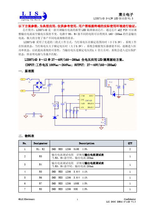
以下方案参数,为典型应用,仅供参考使用,用户需根据终端的实际使用环境进行验证。
芯片简介:LIS8714D是一款可调输出电流的新型LED隔离驱动芯片。
通过芯片ADJ PIN可以调整输出电流而空载电压保持不变。
电路中R3、R4接不同的电阻可以得到从160~280mA的任意输出电流,极大的方便了客户不同电流规格的需求。
LIS8714D 采用了先进的三段式工作方式,当灯珠电压在额定范围内时(小于3.3V),系统工作在恒流状态,当灯珠电压大于额定电压时(大于3.3V),系统会根据变压器感量不同,逐渐进入恒功率状态,以此提高系统的可靠性,当输出电压是额定电压的1.4 倍左右时,系统会进入过压保护状态,即表明电源与负载不匹配。
LIS8714D 8~12串27~40V/160~280mA 全电压应用LED隔离驱动方案。
(INPUT:工作电压100Vac~264Vac; OUTPUT: 27~40V/160~280mA)一.原理图二.物料表No.Designator Description QTY1 R1、R2 SMD RES 1206 510K ±5% 22 R3 输出电流调试电阻 详细见输出电流调试表当R3、R4悬空时,输出电流280mA13 R4 输出电流调试电阻 详细见输出电流调试表当R3、R4悬空时,输出电流280mA14 R5 SMD RES 1206 3.6Ω ±1% 15 R6 SMD RES 1206 3.6Ω ±1% 16 R7 SMD RES 1206 100K ±5% 17 R8 SMD RES 1206 33K ±5% 1三.输出电流调试表R3 (kΩ) ±1%空 75 75 75 75 75 75 75R4 (kΩ) ±1%空 270 200 137 100 82 68 56 (kΩ) ±1%空 58.7 54.5 48.5 42.9 39.2 35.7 32.1R等效输出电流(mA) 280 270 260 240 220 200 180 160注:R3、R4都不接电阻时,输出电流为最大输出电流280mA,当R3、R4可以接任意电阻,使其并联等效电阻设置在32.1kΩ-58.7kΩ之间,从而得到合适的输出电流。
8通道LED驱动器MAX16807
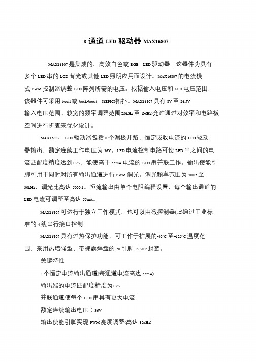
8通道LED驱动器MAX16807MAX16807 是集成的、高效白色或RGB LED 驱动器。
这器件为具有多个LED 串的LCD 背光或其他LED 照明应用而设计。
MAX16807 的电流模式PWM 控制器调整LED 阵列所需的电压。
根据输入电压和LED 电压范围,该器件可采用boost 或buck-boost (SEPIC)拓扑。
MAX16807 具有8V 至26.5V 输入电压范围。
较宽的频率调整范围(20kHz 至1MHz)允许通过对效率和电路板空间进行折衷来优化设计。
MAX16807 LED 驱动器包括8 个漏极开路、恒定吸收电流的LED 驱动器输出,额定连续工作电压为36V。
LED 电流控制电路可使LED 串之间的电流匹配度精度达到±3%,能使高于55mA 电流的LED 串并联工作。
输出使能引脚可用于同时对所有输出通道进行PWM 调光。
调光频率范围为50Hz 至30kHz,调光比高达5000:1。
恒流输出由单个电阻编程设置,每个输出通道的LED 电流可调整至高达55mA。
MAX16807 可运行于独立工作模式,也可以由微控制器(µC)通过工业标准的4 线串行接口控制。
MAX16807 具有过热保护功能,可工作于扩展的-40°C至+125°C温度范围,采用热增强型、带裸露焊盘的28 引脚TSSOP 封装。
关键特性8 个恒定电流输出通道(每通道电流高达55mA)输出端的电流匹配度精度为±3%并联通道使每个LED 串具有更大电流额定连续输出电压:36V输出使能引脚实现PWM 亮度调整(高达30kHz)。
MP3336A-C-00A双通道高功率闪光LED驱动器说明书

EV3336A-C-00ADual-Channel Flash LED DriverWith 2A/Ch and I2C InterfaceDESCRIPTIONThe MP3336A is a compact, dual-channel, high-power, flash LED driver that can drive up to 2A in flash mode for each LED. It is usually applied for camera phones to improve image and video quality in low-light environments. The MP3336A operates with a selectable 1/2/3/4MHz switching frequency and uses a synchronous, current-mode PWM boost converter to regulate the LED current with two high-current sources. The MP3336A provides a high efficiency and optimized solutionfor smaller PCB spaces.The MP3336A features a standard I2C interface, dual LED channels, rich protection modes, and high power density and performances. The MP3336A can also support flash, assist, indicator, and 5V DC modes.The cathodes of the dual-flash LED are referenced to GND, which is better for improving thermal performance in layout. The MP3336A is available in a WLCSP-20 (1.6mmx2.0mm) package.ELECTRICAL SPECIFICATION Parameter SymbolValueUnits Input Voltage V IN 2.7-5.5 V Output Voltage V OUT <5.5 VLEDs # 2LED Current/string I LED Max.2 A FEATURES∙ 2.7V~5.5V Input Voltage∙1/2/3/4MHz Selectable Max Fsw∙Fsw Fold-back Function∙ 400kHz I2C Compatible Interface∙ Standby/Flash/Assist/Indicator/5V DC ModesFlash Mode∙Up to 2A/Ch Programmable Current with ±7% Accuracy for Each LED, 7.84mA/Step Assist Mode∙Up to 319mA/Ch Programmable Current with ±7% Accuracy for Each LED,1.25mA/StepIndicator Mode∙Works in 31.5kHz PWM Dimming Mode with 2/16, 3/16, 4/16, 5/16 Duty Cycle∙Used for Blinking and 128/256/512ms Selectable Blinking Time5V DC Mode∙Output Constant 5V DC Voltage∙Separated EN1 Pin for NFC Application∙1A to 4.2A Programmable Input DC Current Limit Protection∙External Strobe/TX Pin∙VIN to VOUT Disconnection Function∙Low-Battery Voltage Protection∙LED Short/Open Protection∙VOUT-GND Short Protection∙Over-Voltage Protection (OVP)∙Over-Temperature Protection (OTP)∙Input Under-Voltage Lockout (UVLO) Protection∙ WLCSP-20 (1.6mmx2.0mm) Package APPLICATIONS∙Smartphone Flash LED Application∙Cameras for Tablets∙ Digital Still CameraAll MPS parts are lead-free, halogen free, and adhere to the RoHS directive. For MPS green status, please visit MPS website under Quality Assurance. “MPS” and “The Future of Analog IC Technology” are Registered Trademarks of Monolithic Power Systems, Inc.EV3336A-C-00A EVALUATION BOARD(L × W) 5.5cm x 5.5cmBoard Number MPS IC NumberEV3336A-C-00A MP3336AGCEVALUATION BOARD SCHEMATICFigure 1: Dual-Channel Application CircuitEV3336A-C-00A BILL OF MATERIALSQty Ref Value Description Package Manufacturer Manufacturer PN 1 C1 NC 06032 C2,C4 10uFCeramicCapacitor,10V,X5R0805 muRata GRM21BR61A106KE19L 1 C3 NC 0805 3 R1,R6,R7 0 res,1% 0603 Yageo RC0603FR-070RL 4 R2,R3,R4,R5 NC 0603 1 L1 1.1uH 1.1uA, 20m, 3.46A TDK D53LC-#A915AY-1R1M1 U1 MP3336A CSP92.01*1.61mmMPS MP3336APRINTED CIRCUIT BOARD LAYQUICK START GUIDE1. Connect the positive and negative terminals of the power supply (2.7V ~5.5V) to the VIN and GNDpins on the EV board, respectively.2. Supply the EN terminal with logical signal.3. Connect the positive and negative terminals of the LED to the LED1/2 pin and GND on the EVboard, respectively.4. Please connect SCL, SDA and GND of EV board to the SCL, SDA and GND of a programmable kit(EVKT-USBI2C-02) with I2C interface, respectively.5. Power on sequence: VIN →EN →I2C setting → Set LED1/2_EN bit (to light the LED load). Whenwork in flash mode with hardware trigger mode, please give a level or pulse signal to STR pin. NOTICE: The information in this document is subject to change without notice. Users should warrant and guarantee that third party Intellectual Property rights are not infringed upon when integrating MPS products into any application. MPS will not assume any legal responsibility for any said applications.。
QX6001 电容式触摸 无级调光台灯驱动IC
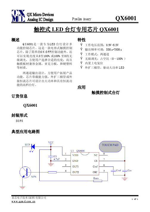
QX6001
触控式 LED 台灯专用芯片 QX6001
概述
QX6001 是 一 款 专 为 LED 台 灯 设 计 多 功能控制芯片。这是一款电容式触摸控制 芯片,除了简单的ON/OFF控制功能外,还 可以实现亮度从0至100%或100%至0的无 级调光,方便用户选择合适的亮度;而且 触摸板材兼容金属,亚克力板,和硬塑料 等材质。
泉芯电子技术(深圳)有限公司
5 of 5
封装信息
Preliminary
QX6001
泉芯电子技术(深圳)有限公司
6 of 6
out1输出端10占空比和100占空比两种状态out2输出端2从0占空比到100占空比状态rcosc振荡频率调节端振荡频率调节cref灵敏度调节触摸感应灵敏度调节cs手指触摸端触摸感应端口ncpreliminaryqx6001泉芯电子技术深圳有限公司wwwqxmdcomcn极限参数符号symbol参数parameter值value单位unitvdd供电电压60out1out2输出端电流120marcosc振荡频率55700hzcref基准电容150pfcs从0100占空比最长时间15操作节点温度20stg保存温度55功能描述无级调光功能
表1 触摸介质材料及厚度对应Cref采样电容表
介质类型
直接触摸金属外壳 0.3mm以内亚克力玻璃
0.3mm硬塑料
器件类型 47pF瓷片电容 22pF瓷片电容 10pF瓷片电容
Cref
器件参数 47pF/10V 22pF/10V 10pF/10V
二、无级调光频率调节
QX6001C 在无级调节模式下的调节频率可以根据客户需求灵活调节。具体调节方式是通过在 RCOSC 端与电源端接入电阻来提高调节开关控制频率。
- 1、下载文档前请自行甄别文档内容的完整性,平台不提供额外的编辑、内容补充、找答案等附加服务。
- 2、"仅部分预览"的文档,不可在线预览部分如存在完整性等问题,可反馈申请退款(可完整预览的文档不适用该条件!)。
- 3、如文档侵犯您的权益,请联系客服反馈,我们会尽快为您处理(人工客服工作时间:9:00-18:30)。
Simple 4 windings to meet No-Y design.
Output Performance :
Better than +/-1.5% load and line regulation.
(b)
Uses extremely low cost BJT MJ13002)
Non Line voltages dependence OCP protection.
2UEW 0.14mmx1 47T – Primary
2UEW 0.14mmx1 47T – Primary
3(S)
2UEW 0.14mmx1 47T – Primary
5V/700mA LED Driver with 1696
iWatt Confidential – Do Not Copy
16 Feb 2009
Appendix – Simple Specification for used BJT(TSC13003CT TO-92)
5V/700mA LED Driver with 1696
iWatt Confidential – Do Not Copy
16 Feb 2009
Item Input Bulk_Cap(C8) Input Bulk_Cap(C1) IC1(iW1696) Transformer(T1) Power Transistor(Q1-BV42) Output Schotty Diode(D9) Ambient (GU10 Housing) Temp.
5V/700mA LED Driver with 1696
iWatt Confidential – Do Not Copy
16 Feb 2009
Page: 5
4.Circuit Board Photograph
Top side
Primary
Secondary
iW1696
Bottom side
5V/700mA LED Driver with 1696
LED Driver Design with iW1696
Summary and Features : 1. LED driver, 5V, CC@0.7A ; Wide AC input range @90Vac- 264Vac 2 For Isolated or Non-isolated Applications 3. High Efficiency and Minimum Parts count 4. Meet EMI EN55015B-QP & AV limits 5. Fully protected against AC input UV, OV, O/P Short/Open, meet single point failure test.
1. Specification
Description
Input Voltage Frequency Open-load Input Power (264VAC) Output Const @ 0-700 m A Voltage Const @ 2.2-4.5 V Current Output Ripple Current Continuous Output Power Output short circuit test Efficiency Others Turn on Delay Time Inrush current Hi-pot test Conducted EMI Surge Test Operation Temperature Topr 50 °C 1 10 4 Meets EN55015B Sec A kV
0
100 200 300 400 500 600 700 800 900 Iout
5V/700mA LED Driver with 1696
iWatt Confidential – Do Not Copy
16 Feb 2009
Page: 9
8. Temperature test
VIN=90Vac, 1X3W LED Temp.(℃) 75 79 74 85 86 90 63 Rising Temp. (℃) 12 16 11 22 23 27 VIN=264Vac,1X3W LED Temp.(℃) 74 74 74 83 84 91 63 Rising Temp. (℃) 11 11 11 20 21 28
iW1696 (NEW) for 1-3W LED ---- Probably lowest cost available..
No RCD Clamp is needed for <2W as BJT consume part of LK energy Extended on-chip frequency differ reduced EMI filtering contents
C8
Q1
T1
U1
D3
C1 PCB_Internal ambient
5V/700mA LED Driver with 1696
iWatt Confidential – Do Not Copy
16 Feb 2009
Page: 10
9. VDS waveform
Test Condition: VIN=264VAC,IOUT=0.35A Result:x10 Vce_MAX=514V
η
Differential mode
Free convection, sea level
5V/700mA LED Driver with 1696
iWatt Confidential – Do Not Copy
16 Feb 2009
Page: 3
2.Schematic circuit
5V/700mA LED Driver with 1696
5V/700mA LED Driver with 1696 iWatt Confidential – Do Not Copy 16 Feb 2009 Page: 8
7. Output VI Characteristics
* Note: Output voltage measured at PCB end, TAMB=25 ℃
Bobbin position for clockwise direction
6 Bias 5
5(F)
2UEW 0.19 32T –Bias
6(S) B(F)
0.35mmx1 12T –Secondary Triple Insulation wire
ELECTRICAL SPECIFICATIONS: 1. Primary Inductance (Lp) = 3mH @10KHz 2. Primary Leakage Inductance (Lk)≤100uH@10KHz MATERIALS: 1. Core : EE13 (Ferrite Material TDK PC40 or equivalent) 2. Bobbin : EE13 Horizontal 3. Magnet Wires : Type 2-UEW 4. Layer Insulation Tape :3M1298 or equivalent. FINISHED :
iWatt Confidential – Do Not Copy
16 Feb 2009
Page: 6
5. Transformer Design
SCHEMATIC 4 Primary 3 188T A 12T B 32T
电气同名端
Pin 4 Pin 1
Winding Direction
Pin 5
Winding machine
Page: 7
6. Regulation, Efficiency Measurement
70
60
50
Eff(%)
40
30
20
10
0 80 100 120 140 160 180 Vin(Vac) 200 220 240 260 280
* Note: Output voltage measured at end of PCB.
iW1696
Embedded Secondary real-time OVP protection eliminate external Zener and voltage margin needed for O/P cap.
*Cost **Performance Cost & Performance 5V/700mA LED Driver with 1696 Digitally operated multi-mode VMS controller for high efficiency design. (>69%@230Vac); (>55%@3.3V/50mA) iWatt Confidential – Do Not Copy 16 Feb 2009 Page: 2
VIN=90VAC, TAMB=25℃
VIN=264VAC, TAMB=25℃
Vout
V-I Curve Vout 6 5.5 5 4.5 4 3.5 3 2.5
V-I Curve
6 5.5 5 4.5 4 3.5 3 2.5 0 100 200 300 400 500 600 700 800 900 Iout
Units
VAC Hz W
2 Wire
Comment
VOUT_CV IOUT_CV 0.6
3.5 0.7
5 0.75
V A mA
Measured at the PCB connector
Measured at the LED load