1N5247B-T中文资料
1N5247B-A中文资料

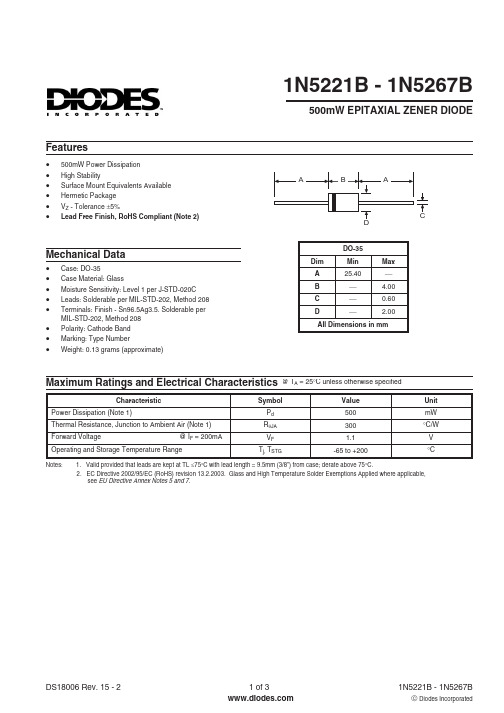
1N5221B - 1N5267B500mW EPITAXIAL ZENER DIODEFeaturesMaximum Ratings and Electrical Characteristics@ T A = 25°C unless otherwise specified·Case: DO-35·Case Material: Glass·Moisture Sensitivity: Level 1 per J-STD-020C ·Leads: Solderable per MIL-STD-202, Method 208·Terminals: Finish - Sn96.5Ag3.5. Solderable per MIL-STD-202, Method 208·Polarity: Cathode Band ·Marking: Type Number·Weight: 0.13 grams (approximate)·500mW Power Dissipation ·High Stability·Surface Mount Equivalents Available ·Hermetic Package·V Z - Tolerance ±5%·Lead Free Finish, RoHS Compliant (Note 2)Mechanical DataNotes:1. Valid provided that leads are kept at TL £75°C with lead length = 9.5mm (3/8”) from case; derate above 75°C.2.EC Directive 2002/95/EC (RoHS) revision 13.2.2003. Glass and High Temperature Solder Exemptions Applied where applicable,see EU Directive Annex Notes 5 and 7.Electrical Characteristics Table 1@ T A= 25°C unless otherwise specifiedNotes: 3. Based on dc measurement at thermal equilibrium; lead length = 9.5mm (3/8”); thermal resistance of heat sink = 30°C/W.Ordering Information(Note 5)Notes: 4. *Add "-A" or "-T" to the appropriate type number in Table 1. Example: 6.2V Zener= 1N5234B-A for ammo pack.5. For packaging details, visit our website at /datasheets/ap02008.pdf.IMPORTANT NOTICEDiodes Incorporated and its subsidiaries reserve the right to make modifications,enhancements,improvements,corrections or other changes without further notice to any product herein.Diodes Incorporated does not assume any liability arising out of the application or use of any product described herein;neither does it convey any license under its patent rights,nor the rights of others.The user of products in such applications shall assume all risks of such use and will agree to hold Diodes Incorporated and all the companies whose products are represented on our website,harmless against all damages.LIFE SUPPORTDiodes Incorporated products are not authorized for use as critical components in life support devices or systems without the expressed written approval of the President of Diodes Incorporated.。
547B资料

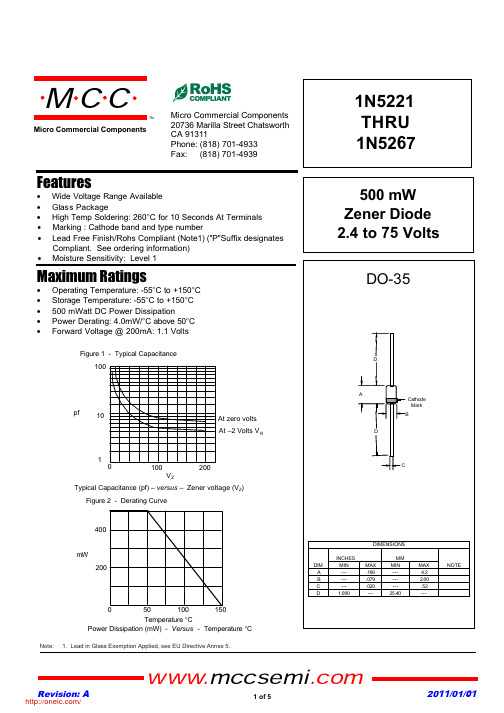
MCC
VBE(on) @ VCE = 10 V
VCE(sat) @ IC/IB = 10 0.2 0.3 0.5 0.7 1.0 2.0 3.0 5.0 7.0 10 20 30 IC, COLLECTOR CURRENT (mAdc) 50 70 100
Figure 1. Normalized DC Current Gain
OFF CHARACTERISTICS
Collector–Emitter Breakdown Voltage (IC = 1.0 mA, IB = 0) Collector–Base Breakdown Voltage (IC = 100 µAdc) Emitter–Base Breakdown Voltage (IE = 10 mA, IC = 0)
V(BR)CBO
V
V(BR)EBO
V
ON CHARACTERISTICS
DC Current Gain (IC = 10 µA, VCE = 5.0 V) hFE BC547A/548A BC546B/547B/548B BC548C BC546 BC547 BC548 BC547A/548A BC546B/547B/548B BC547C/BC548C BC547A/548A BC546B/547B/548B BC548C VCE(sat) — VBE(sat) VBE(on) 0.55 — — — 0.7 0.77 — — — — 110 110 110 110 200 420 — — — 90 150 270 — — — 180 290 520 120 180 300 --— — — — 450 800 800 220 450 800 — — — V 0.3 1.0 V V —
1N4007(Hitano Enterprise)中文数据手册「EasyDatasheet」

芯片中文手册,看全文,戳
奇彦企业股份有限公司. 1N4001 THRU 1N4007
典型结电容(注)
@T = 25 C @T = 100 Cຫໍສະໝຸດ 典型热阻 工作和存储温度范围
注意: 测得1 MH
和应用4.0伏特反向电压
符号
V V V
I
I V
I
C R T,T
1N4001 50 35 50
1N4002 100 70 100
1N4003 200 140 200
1N4004 1N4005 400 600 280 420 400 600
DO-41
最大额定值,电器性能
在25℃环境温度额定值除非另有规定. 单相,半波,60赫兹,电阻或电感性负载.
对于容性负载,减免电流20%.
尺寸以英寸(毫米)
最大经常峰值反向电压
最大RMS电压
最大直流阻断电压
最大正向平均整流电流
在T = 75 C 峰值正向浪涌电流8.3ms单一正弦半波 叠加额定负荷(JEDEC方法) 最大正向电压在1.0A DC 反向电流最大DC 在额定阻断电压DC 满载最大反向电流平均值,完整周期 .375 *设计(9.5mm)引线长度在T = 75 C
1N4006 800 560 800
1N4007 1000 700 1000
UNITS Volts Volts Volts
1.0
Amps
30 1.1 5.0 500
1N5258B-T中文资料
1N5221B - 1N5267B500mW EPITAXIAL ZENER DIODEFeaturesMaximum Ratings and Electrical Characteristics@ T A = 25°C unless otherwise specified·Case: DO-35·Case Material: Glass·Moisture Sensitivity: Level 1 per J-STD-020C ·Leads: Solderable per MIL-STD-202, Method 208·Terminals: Finish - Sn96.5Ag3.5. Solderable per MIL-STD-202, Method 208·Polarity: Cathode Band ·Marking: Type Number·Weight: 0.13 grams (approximate)·500mW Power Dissipation ·High Stability·Surface Mount Equivalents Available ·Hermetic Package·V Z - Tolerance ±5%·Lead Free Finish, RoHS Compliant (Note 2)Mechanical DataNotes:1. Valid provided that leads are kept at TL £75°C with lead length = 9.5mm (3/8”) from case; derate above 75°C.2.EC Directive 2002/95/EC (RoHS) revision 13.2.2003. Glass and High Temperature Solder Exemptions Applied where applicable,see EU Directive Annex Notes 5 and 7.Electrical Characteristics Table 1@ T A= 25°C unless otherwise specifiedNotes: 3. Based on dc measurement at thermal equilibrium; lead length = 9.5mm (3/8”); thermal resistance of heat sink = 30°C/W.Ordering Information(Note 5)Notes: 4. *Add "-A" or "-T" to the appropriate type number in Table 1. Example: 6.2V Zener= 1N5234B-A for ammo pack.5. For packaging details, visit our website at /datasheets/ap02008.pdf.IMPORTANT NOTICEDiodes Incorporated and its subsidiaries reserve the right to make modifications,enhancements,improvements,corrections or other changes without further notice to any product herein.Diodes Incorporated does not assume any liability arising out of the application or use of any product described herein;neither does it convey any license under its patent rights,nor the rights of others.The user of products in such applications shall assume all risks of such use and will agree to hold Diodes Incorporated and all the companies whose products are represented on our website,harmless against all damages.LIFE SUPPORTDiodes Incorporated products are not authorized for use as critical components in life support devices or systems without the expressed written approval of the President of Diodes Incorporated.。
外贸单据中英文对照a

销货合同SALES CONTRACT卖方SELLER:WENSLI GROUP.#309 JICHANG RD,HANGZHOU,CHINATEL:86-25-4729178 FAX:82-25-4715619 编号NO.:NEO2010/026 日期DATE:Aug. 20, 2010 地点SIGNEDIN:HANGZHOUO,CHINA买方BUYER:N.E.ORIENTAL TRADING CO.LTD.P.O. BOX 12345 CODE 55400 T-3456789 RIYADH KINGDOM OF SAUDI ARABIA买卖双方同意以下条款达成交易:This contract Is made by and agreed between the BUYER and SELLER , in accordance with the terms and conditions stipulated below.1. 品名及规格Commodity & Specification2. 数量Quantity3. 单价及价格条款Unit Price & TradeTerms4. 金额AmountCIF DAMMAM PORT, SAUDI ARABIA400 BUNDLES TEXTILE FABRIC 200 BUNDLES LADIES’ SUIT400 BUNDLES200 BUNDLESUSD120.00USD50.00USD58000.00Total:600 BUNDLES USD58000.00允许5% 溢短装,由卖方决定With More or less of shipment allowed at the sellers’ option 5. 总值Total ValueUSD FIFTY EIGHT THOUSAND ONLY.6. 包装PackingBUNDLE7. 唛头Shipping Marks N.E OTNEO2010/026 DAMMAM PORT B/N 1-6008. 装运期及运输方式Time of Shipment & means ofTransportationNot Later Than Oct. 20, 2010 BY VESSEL9. 装运港及目的地Port of Loading &Destination From : SHANGHAI, CHINATo : DAMMAM PORT, SAUDI ARABIA10. 保险Insurance TO BE COVERED BY SELLER AGAINST WPA AND WAR RISKS FOR 110% OF THE INVOICE VALUE AS PER THE RELEVANT OCEAN MARINE CARGO OF PICC DATED 1/1/198111. 付款方式Terms ofPayment By Irrevocable Letter of Credit to be opened by full amount of L/C, Payment at Sight document to e presented within 21 days after date of B/L at beneficiary's account.12. 备注Remarks1) Transshipment prohibited, Partial shipment prohibited.2) Shipment terms will be fulfilled according to the L/C finally. The Buyer The SellerN.E.ORIENTAL TRADING CO.LTD.(进口商签字盖章) WENSLI GROUP. (出口商签字和盖章)ISSUER装箱单PACKING LISTWENSLI GROUP.#309 JICHANG RD,HANGZHOU,CHINA TEL:86-25-4729178 FAX:82-25-4715619TON.E.ORIENTAL TRADING CO.LTD. P.O. BOX 12345 CODE 55400 T-3456789 RIYADH KINGDOM OFSAUDI ARABIAINVOICE NO.DATE 2010SDT0012010.08.22Marks and Numbers Number and kind of package Description of goodsPACKAGE G.WN.W Meas.KGCBMN.E OT NEO2010/026DAMMAM PORT B/N 1-600400 BUNDLES TEXTILE FABRIC 200 BUNDLES LADIES' SUIT400 BUNDLES 200 BUNDLES6000KGS 3000KGS5800KGS 2900KGSTOTAL 600 BUNDLES 9000KGS 8700KGS TOTAL PACKED IN 600 BUNDLES(出口商签字和盖单据章)WENSLI GROUP.ISSUERWENSLI GROUP.#309 JICHANG RD,HANGZHOU,CHINATEL:86-25-4729178 FAX:82-25-4715619商业发票COMMERCIAL INVOICE TON.E.ORIENTAL TRADING CO.LTD.P.O. BOX 12345 CODE 55400 T-3456789 RIYADH KINGDOM OF SAUDI ARABIA NO.2010SDT001DATE2010.10.11TRANSPOR T DETAI L SSHIPMENT FROM SHANGHAI TO DAMMAM PORT BY SEA S/C NO.NEO2010/026L/C NO.DES505606TERMS OF PAYME N TL/C AT SIGHTMarks and Numbers Number and kind of packageDescription of goods Quant ity Unit Price AmountUSDN.E OTNEO2010/026 DAMMAM PORT B/N 1-600C F RDAMMAMPO RT,S A UDI A RA BIA400 BUNDLES TEXTILE FABRIC200 BUNDLES LADIES' SUIT400 BUNDLES200 BUNDLESUSD120.00USD50.00USD58000.00Total:600 BUNDLES USD58000.00SAY T OTAL:SAY USD FIFTY EIGH T TH OUSAND ONLY.We hereby certify that the contents of invoice herein are ture and correct.DESUNSOFT TRADING COMPANY(出口商签字和盖单据章)WENSLI GROUP.出口货物明细单银行编号HJL20100630外运编号DSINV201077777核销单号1234567890许可证号0111010经营单位(装船人)WENSLI GROUP.#309 JICHANG RD,HANGZHOU,CHINATEL:86-25-4729178 FAX:82-25-4715619合同号NEO2010/026信用证号DES505606开证日期2010.10.12收到日期2010.10.14提单或承运收据抬头人TO THE ORDER OF SHIPPER金额USD58000.00收汇方式L/C贸易国别SAUDI ARABIA消费国别SAUDI ARABIA 通知人HANGZHOU AJFINANCECORPORATION59 QINGCHUN RDHANGZHOU CHINA出口口岸SHANGHAI目的港DAMMAM PORT可否转运NO可否分批NO运费FREIGHT PREPAIED装运期限2010.10.15有效期限2010.10.20标记唛头N.E OTNEO2010/026DAMMAM PORTB/N 1-600货物描述STYLE NO.PONO.QTY/PCS UNIT PRICE (USD) CIF DAMMAM PORT400 BUNDLES USD120.00200 BUNDLES USD50.00TOTAL600 BUNDLESPACKED IN 600 BUNDLES ONLY.TOTAL G.W.: 9000KGSTOTAL N.W.: 8700KGSCOUNTRY OF ORIGIN: P.R.CHINA(出口商盖出口货物明细专用章)WENSLI GROUP.本公司注意事项总体积保险单险别WPA AND WAR RISKS保额USD63800.00赔款地点SAUDI ARABIA外运外轮注意事项B/L ISSUED BY W.T. SHIPPING OR THEIR AGENTS.B/L MUST SPECIFY THE NAME OF LOADING PORT ANDDISCHARGING PORT.船名SKY BRIGHT V.047A海关编号60019200006110.300090放行日期制单员报检委托书出入境检验检疫局:上海出入境检验检疫局本委托人声明,保证遵守《中华人民共和国进出口商品检验法》、《中华人民共和国进出境动植物检疫法》、《中华人民共和国国境卫生检疫法》、《中华人民共和国食品卫生法》等有关法律、法规的规定和检验检疫机构制定的各项规章制度。
1N5230B-A中文资料

1N5221B - 1N5267B500mW EPITAXIAL ZENER DIODEFeaturesMaximum Ratings and Electrical Characteristics@ T A = 25°C unless otherwise specified·Case: DO-35·Case Material: Glass·Moisture Sensitivity: Level 1 per J-STD-020C ·Leads: Solderable per MIL-STD-202, Method 208·Terminals: Finish - Sn96.5Ag3.5. Solderable per MIL-STD-202, Method 208·Polarity: Cathode Band ·Marking: Type Number·Weight: 0.13 grams (approximate)·500mW Power Dissipation ·High Stability·Surface Mount Equivalents Available ·Hermetic Package·V Z - Tolerance ±5%·Lead Free Finish, RoHS Compliant (Note 2)Mechanical DataNotes:1. Valid provided that leads are kept at TL £75°C with lead length = 9.5mm (3/8”) from case; derate above 75°C.2.EC Directive 2002/95/EC (RoHS) revision 13.2.2003. Glass and High Temperature Solder Exemptions Applied where applicable,see EU Directive Annex Notes 5 and 7.Electrical Characteristics Table 1@ T A= 25°C unless otherwise specifiedNotes: 3. Based on dc measurement at thermal equilibrium; lead length = 9.5mm (3/8”); thermal resistance of heat sink = 30°C/W.Ordering Information(Note 5)Notes: 4. *Add "-A" or "-T" to the appropriate type number in Table 1. Example: 6.2V Zener= 1N5234B-A for ammo pack.5. For packaging details, visit our website at /datasheets/ap02008.pdf.IMPORTANT NOTICEDiodes Incorporated and its subsidiaries reserve the right to make modifications,enhancements,improvements,corrections or other changes without further notice to any product herein.Diodes Incorporated does not assume any liability arising out of the application or use of any product described herein;neither does it convey any license under its patent rights,nor the rights of others.The user of products in such applications shall assume all risks of such use and will agree to hold Diodes Incorporated and all the companies whose products are represented on our website,harmless against all damages.LIFE SUPPORTDiodes Incorporated products are not authorized for use as critical components in life support devices or systems without the expressed written approval of the President of Diodes Incorporated.。
1N5248B-TR中文资料

1N5221B to 1N5267BDocument Number 85588Rev. 1.7, 23-Mar-07Vishay Semiconductors194 9367Small Signal Zener DiodesFeatures•Silicon Planar Power Zener Diodes•Standard Zener voltage tolerance is ± 5 %•These diodes are also available in Mini-MELF case with the type designationTZM5221 ... TZM5267, SOT23 case with the type designations MMBZ5225 ... MMBZ5267 and SOD123 case with the types designations MMSZ5225 ... MMSZ5267 •Lead (Pb)-free component•Component in accordance to RoHS 2002/95/EC and WEEE 2002/96/ECApplications•Voltage stabilizationMechanical DataCase: DO35 Glass case Weight: approx. 125 mg Cathode Band Color: black Packaging codes/options:TAP/10 k per Ammopack (52 mm tape), 30 k/box TR/10 k per 13" reel, 30 k/boxAbsolute Maximum RatingsT amb = 25°C, unless otherwise specifiedThermal CharacteristicsT amb = 25°C, unless otherwise specifiedElectrical CharacteristicsT amb = 25°C, unless otherwise specifiedParameterTest conditionSymbol Value Unit Power dissipation T L ≤ 25°CP tot 500mW Z-currentI ZP tot /V ZmAParameterTest conditionSymbol Value Unit Thermal resistance junction to ambient air l = 4 mm, T L = constantR thJA 300K/W Junction temperature T j 175°C Storage temperature rangeT stg- 65 to + 175°CParameterT est conditionSymbol MinT yp.Max Unit Forward voltageI F = 200 mAV F1.1V 2Document Number 85588Rev. 1.7, 23-Mar-071N5221B to 1N5267B Vishay SemiconductorsElectrical Characteristics1N5221B...1N5267BPartnumber Nominal ZenerVoltage1)T est Current MaximumDynamicImpedance1)MaximumDynamicImpedanceTypicalTemperature ofCoeffizientMaximum Reverse LeakageCurrentat I ZT, V Z I ZT Z ZT at I ZT Z ZK at I ZK =0.25 mAat I ZT I R V R V mAΩΩα (%/K)µA V 1N5221B 2.420301200- 0.0851001 1N5222B 2.520301250- 0.0851001 1N5223B 2.720301300- 0.080751 1N5224B 2.820301400- 0.080751 1N5225B320291600- 0.075501 1N5226B 3.320281600- 0.070251 1N5227B 3.620241700- 0.065151 1N5228B 3.920231900- 0.060101 1N5229B 4.320222000+ 0.05551 1N5230B 4.720191900+ 0.03052 1N5231B 5.120171600+ 0.03052 1N5232B 5.620111600+ 0.03853 1N5233B62071600+ 0.0385 3.5 1N5234B 6.22071000+ 0.04554 1N5235B 6.8205750+ 0.05035 1N5236B7.5206500+ 0.05836 1N5237B8.2208500+ 0.0623 6.5 1N5238B8.7208600+ 0.0653 6.5 1N5239B9.12010600+ 0.06837 1N5240B102017600+ 0.07538 1N5241B112022600+ 0.07628.4 1N5242B122030600+ 0.07719.1 1N5243B139.513600+ 0.0790.59.9 1N5244B14915600+ 0.0820.110 1N5245B158.516600+ 0.0820.111 1N5246B167.817600+ 0.0830.112 1N5247B177.419600+ 0.0840.113 1N5248B18721600+ 0.0850.114 1N5249B19 6.623600+ 0.0860.114 1N5250B20 6.225600+ 0.0860.115 1N5251B22 5.629600+ 0.0870.117 1N5252B24 5.233600+ 0.0880.118 1N5253B25535600+ 0.0890.119 1N5254B27 4.641600+ 0.0900.121 1N5255B28 4.544600+ 0.0910.121 1N5256B30 4.249600+ 0.0910.123 1N5257B33 3.858700+ 0.0920.125 1N5258B36 3.470700+ 0.0930.127 1N5259B39 3.280800+ 0.0940.130 1N5260B43393900+ 0.0950.133 1N5261B47 2.71051000+ 0.0950.136 1N5262B51 2.51251100+ 0.0960.139 1N5263B56 2.21501300+ 0.0960.143 1N5264B60 2.11701400+ 0.0970.1461N5221B to 1N5267BDocument Number 85588Rev. 1.7, 23-Mar-07Vishay Semiconductors31)Based on dc-measurement at thermal equilibrium; lead length = 9.5 (3/8 "); thermal resistance of heat sink = 30 K/WTypical CharacteristicsT amb = 25°C, unless otherwise specified1N5265B 6221851400+ 0.0970.1471N5266B 68 1.82301600+ 0.0970.1521N5267B751.72701700+ 0.0980.156PartnumberNominal Zener Voltage1)Test CurrentMaximum Dynamic Impedance 1)Maximum DynamicImpedance T ypical T emperature of CoeffizientMaximum Reverse LeakageCurrentat I ZT , V ZI ZT Z ZT at I ZTZ ZK at I ZK = 0.25 mAat I ZT I R V R VmA ΩΩα (%/K)µA V Figure 1. Thermal Resistance vs. Lead LengthFigure 2. Typical Change of Working Voltage under OperatingConditions at T amb = 25 °C95 9611510150100200300400500R t h J A - T h e r m . R e s i s t . J u n c t i o n A m b i e n t (K /W )I - Lead Length (mm)1015201101001000V Z - V o l t a g e C h a n g e (m V )V Z - Z-V oltage (V )95 959805Figure 3. Typical Change of Working Voltage vs.Junction TemperatureFigure 4. Total Power Dissipation vs. Ambient Temperature0.V Z t n - R e l a t i v e V o l t a g e C h a n g eT j - J u nction Temperat u re (°C)95 95991201600100300400500600P t o t - T o t a l P o w e r D i s s i p a t i o n (m W )T am b - Am b ient Temperat u re (°C)20095 96022008040 4Document Number 85588Rev. 1.7, 23-Mar-071N5221B to 1N5267BVishay SemiconductorsFigure 5. Temperature Coefficient of Vz vs. Z-Voltage Figure 6. Diode Capacitance vs. Z-Voltage Figure 7. Forward Current vs. Forward Voltage 30- 551015V Z - Z-V oltage (V )5095 96004010200T K V Z - T e m p e r a t u r e C o e f f i c i e n t o f V Z (10-4/K )1015C D - D i o d e C a p a c i t a n c e (p F )V Z - Z-V oltage (V )95 96012050.010.11010095 9605I F - F o r w a r d C u r r e n t (m A )VF - For w ard V oltage (V )Figure 8. Z-Current vs. Z-VoltageFigure 9. Z-Current vs. Z-VoltageFigure 10. Differential Z-Resistance vs. Z-Voltage895 960420406080I Z - Z -C u r r e n t (m A )46V Z - Z-V oltage (V )152025300I Z -Z -C u r r e n t (m A )V Z - Z-V oltage (V )95 96071101001000(Ω)95 9606V Z - Z-V oltage (V )r Z - D i f f e r e n t i a l Z -R e s i s t a n c e1N5221B to 1N5267BDocument Number 85588Rev. 1.7, 23-Mar-07Vishay Semiconductors5Package Dimensions in millimeters (inches): DO35Figure 11. Thermal ResponseZ t h p - T h e r m a l R e s i s t a n c e f o r P u l s e C o n d . (K W )t P - P u lse Length (ms)95 960310-1100101102 6Document Number 85588Rev. 1.7, 23-Mar-071N5221B to 1N5267BVishay SemiconductorsOzone Depleting Substances Policy StatementIt is the policy of Vishay Semiconductor GmbH to1.Meet all present and future national and international statutory requirements.2.Regularly and continuously improve the performance of our products, processes, distribution and operatingsystems with respect to their impact on the health and safety of our employees and the public, as well as their impact on the environment.It is particular concern to control or eliminate releases of those substances into the atmosphere which are known as ozone depleting substances (ODSs).The Montreal Protocol (1987) and its London Amendments (1990) intend to severely restrict the use of ODSs and forbid their use within the next ten years. Various national and international initiatives are pressing for an earlier ban on these substances.Vishay Semiconductor GmbH has been able to use its policy of continuous improvements to eliminate the use of ODSs listed in the following documents.1.Annex A, B and list of transitional substances of the Montreal Protocol and the London Amendmentsrespectively2.Class I and II ozone depleting substances in the Clean Air Act Amendments of 1990 by the EnvironmentalProtection Agency (EPA) in the USA3.Council Decision 88/540/EEC and 91/690/EEC Annex A, B and C (transitional substances) respectively. Vishay Semiconductor GmbH can certify that our semiconductors are not manufactured with ozone depleting substances and do not contain such substances.We reserve the right to make changes to improve technical designand may do so without further notice.Parameters can vary in different applications. All operating parameters must be validated for each customer application by the customer. Should the buyer use Vishay Semiconductors products for any unintended or unauthorized application, the buyer shall indemnify Vishay Semiconductors against all claims, costs, damages, and expenses, arising out of, directly or indirectly, any claim of personal damage, injury or death associatedwith such unintended or unauthorized use.Vishay Semiconductor GmbH, P.O.B. 3535, D-74025 Heilbronn, GermanyDocument Number: 91000Revision: 18-Jul-081DisclaimerLegal Disclaimer NoticeVishayAll product specifications and data are subject to change without notice.Vishay Intertechnology, Inc., its affiliates, agents, and employees, and all persons acting on its or their behalf (collectively, “Vishay”), disclaim any and all liability for any errors, inaccuracies or incompleteness contained herein or in any other disclosure relating to any product.Vishay disclaims any and all liability arising out of the use or application of any product described herein or of any information provided herein to the maximum extent permitted by law. The product specifications do not expand or otherwise modify Vishay’s terms and conditions of purchase, including but not limited to the warranty expressed therein, which apply to these products.No license, express or implied, by estoppel or otherwise, to any intellectual property rights is granted by this document or by any conduct of Vishay.The products shown herein are not designed for use in medical, life-saving, or life-sustaining applications unless otherwise expressly indicated. Customers using or selling Vishay products not expressly indicated for use in such applications do so entirely at their own risk and agree to fully indemnify Vishay for any damages arising or resulting from such use or sale. Please contact authorized Vishay personnel to obtain written terms and conditions regarding products designed for such applications.Product names and markings noted herein may be trademarks of their respective owners.元器件交易网。
1N5241中文资料
Maximum Reverse Leakage Current Test Voltage IR (µA) 50 25 15 10 5.0 5.0 5.0 5.0 5.0 5.0 3.0 3.0 3.0 3.0 3.0 3.0 2.0 1.0 0.5 0.1 0.1 0.1 0.1 0.1 0.1 0.1 0.1 0.1 0.1 0.1 0.1 0.1 0.1 0.1 0.1 0.1 0.1 0.1 0.1 0.1 0.1 0.1 0.1 VR (V) 1.0 1.0 1.0 1.0 1.0 2.0 2.0 3.0 3.5 4.0 5.0 6.0 6.5 6.5 7.0 8.0 8.4 9.1 9.9 10 11 12 13 14 14 15 17 18 19 21 21 23 25 27 30 33 36 39 43 46 47 52 56
元器件交易网
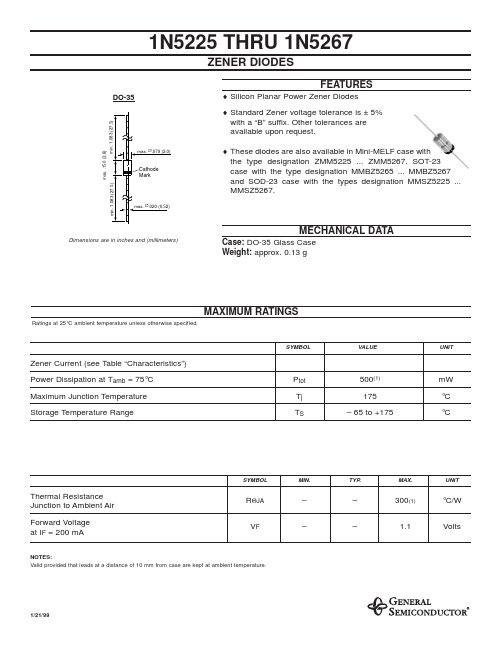
1N5225 THRU 1N5267
ZENER DIODES
FEATURES
DO-35
min. 1.083 (27.5)
♦ Silicon Planar Power Zener Diodes ♦ Standard Zener voltage tolerance is ± 5% with a “B” suffix. Other tolerances are available upon request.
NOTES: (1) The Zener impedance is derived from the 1 kHz AC voltage which results when an AC current having an RMS value equal to 10% of the Zener current (IZT or IZK) is superimposed on IZT or IZK. Zener impedance is measured at two points to insure a sharp knee on the breakdown curve and to eliminate unstable units (2) Valid provided that leads at a distance of 10 mm from case are kept at ambient temperature (3) Measured with device junction in thermal equilibrium
1N5226B中文资料

1N5226B - 1N5257B SeriesDO-35©1997 Fairchild Semiconductor Corporation1N5200B Rev. A1N5226B - 1N5257B SeriesTRADEMARKSACEx™CoolFET™CROSSVOLT™E 2CMOS TM FACT™FACT Quiet Series™FAST ®FASTr™GTO™HiSeC™The following are registered and unregistered trademarks Fairchild Semiconductor owns or is authorized to use and is not intended to be an exhaustive list of all such trademarks.LIFE SUPPORT POLICYFAIRCHILD’S PRODUCTS ARE NOT AUTHORIZED FOR USE AS CRITICAL COMPONENTS IN LIFE SUPPORTDEVICES OR SYSTEMS WITHOUT THE EXPRESS WRITTEN APPROV AL OF FAIRCHILD SEMICONDUCTOR CORPORA TION.As used herein:ISOPLANAR™MICROWIRE™POP™PowerTrench™QS™Quiet Series™SuperSOT™-3SuperSOT™-6SuperSOT™-8TinyLogic™1. Life support devices or systems are devices or systems which, (a) are intended for surgical implant intothe body, or (b) support or sustain life, or (c) whosefailure to perform when properly used in accordancewith instructions for use provided in the labeling, can be reasonably expected to result in significant injury to the user.2. A critical component is any component of a lifesupport device or system whose failure to perform can be reasonably expected to cause the failure of the life support device or system, or to affect its safety or effectiveness.PRODUCT STATUS DEFINITIONS Definition of TermsDatasheet Identification Product Status Definition Advance InformationPreliminary No Identification Needed Obsolete This datasheet contains the design specifications for product development. Specifications may change in any manner without notice.This datasheet contains preliminary data, andsupplementary data will be published at a later date.Fairchild Semiconductor reserves the right to make changes at any time without notice in order to improve design.This datasheet contains final specifications. Fairchild Semiconductor reserves the right to make changes at any time without notice in order to improve design.This datasheet contains specifications on a product that has been discontinued by Fairchild semiconductor.The datasheet is printed for reference information only.Formative or In DesignFirst ProductionFull ProductionNot In ProductionDISCLAIMERFAIRCHILD SEMICONDUCTOR RESERVES THE RIGHT TO MAKE CHANGES WITHOUT FURTHER NOTICE TO ANY PRODUCTS HEREIN TO IMPROVE RELIABILITY , FUNCTION OR DESIGN. FAIRCHILD DOES NOT ASSUME ANY LIABILITY ARISING OUT OF THE APPLICATION OR USE OF ANY PRODUCT OR CIRCUIT DESCRIBED HEREIN; NEITHER DOES IT CONVEY ANY LICENSE UNDER ITS PATENT RIGHTS, NOR THE RIGHTS OF OTHERS.。
1N5245BT中文资料

ZZK
(Ω ) 1,200 1,250 1,300 1,400 1,600 1,600 1,700 1,900 2,000 1,900 1,600 1,600 1,600 1,000 750 500 500 600 600 600 600 600 600 600 600
IR
(%/°C) 0.083 0.084 0.085 0.085 0.086 0.087 0.088 0.088 0.089 0.090 0.091 0.092 0.093 0.094 0.095 0.095 0.096 0.096 0.097 0.097 0.097 0.098 0.098 0.099 0.099 0.099 0.11 0.11 0.11 0.11 0.11 0.11 0.11 0.11
ZZK
(Ω) 600 600 600 600 600 600 600 600 600 600 600 700 700 800 900 1000 1100 1300 1400 1400 1600 1700 2000 2200 2300 2600 3000 4000 4500 4500 5000 5500 5500 6000
Device
1N5246BT 1N5247BT 1N5248BT 1N5249BT 1N5250BT 1N5251B 1N5252B 1N5253B 1N5254B 1N5255B 1N5256B 1N5257B 1N5258B 1N5259B 1N5260B 1N5261B 1N5262B 1N5263B 1N5264B 1N5265B 1N5266B 1N5267B 1N5268B 1N5269B 1N5270B 1N5271B 1N5272B 1N5273B 1N5274B 1N5275B 1N5276B 1N5277B 1N5278B 1N5279B
1N5246B-TP;1N5230B-TP;1N5238B-TP;1N5258B-TP;1N5223B-TP;中文规格书,Datasheet资料
1200 1250 1300 1400 1600 1600 1700 1900 2000 1900 1600 1600 1600 1000 750 500 500 600 600 600 600 600 600 600 600 600 600 600 600 600 600 600 600 600 600 600 700 700 800 900 1000 1100 1300 1400 1400 1600 1700
1.0 1.0 1.0 1.0 1.0 1.0 1.0 1.0 1.0 2.0 2.0 3.0 3.5 4.0 5.0 6.0 6.5 6.5 7.0 8.0 8.4 9.1 9.9 10 11 12 13 14 14 15 17 18 19 21 21 23 25 27 30 33 36 39 43 46 47 52 56
/ Revision: A
2 of 5
20Байду номын сангаас1/01/01
1N5221 1N thru 1N5267
Figure 1 Zener Voltage versus Zener Current – Vz =1 thru 16 Volts 20 10
MCC
Micro Commercial Components
TA=25к
TM
1 mA 0.1
0.01 1 1
2
3
4
5
6
7
8 VOLTS
9
10
11
12
13
14
15
16
IZ , ZENER CURRENT - mA VZ , ZENER VOLTAGE - V
Figure 2 Zener Voltage versus Zener Current – Vz =15 thru 30 Volts 20 10
1N5347B中文资料
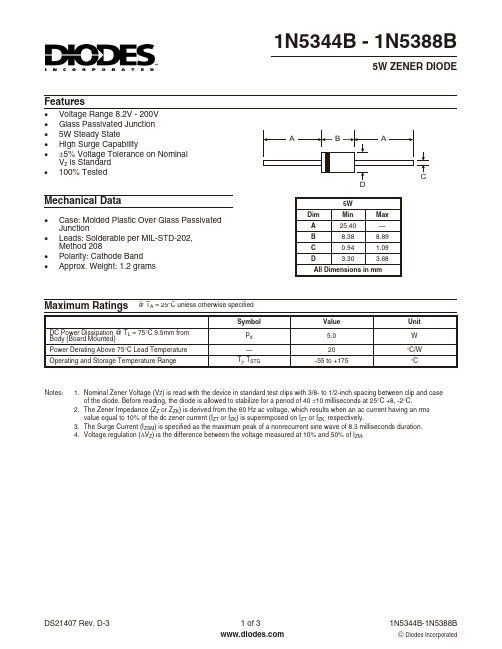
·Voltage Range 8.2V - 200V ·Glass Passivated Junction ·5W Steady State·High Surge Capability·±5% Voltage Tolerance on Nominal V Z is Standard ·100% Tested1N5344B - 1N5388B5W ZENER DIODENotes:1.Nominal Zener Voltage (V Z ) is read with the device in standard test clips with 3/8- to 1/2-inch spacing between clip and case of the diode. Before reading, the diode is allowed to stabilize for a period of 40 ±10 milliseconds at 25°C +8, -2°C.2.The Zener Impedance (Z Zor Z ZK ) is derived from the 60 Hz ac voltage, which results when an ac current having an rmsvalue equal to 10% of the dc zener current (I ZT or I ZK ) is superimposed on I ZT or I ZK, respectively.3.The Surge Current (I ZSM ) is specified as the maximum peak of a nonrecurrent sine wave of 8.3 milliseconds duration.4.Voltage regulation (D V Z ) is the difference between the voltage measured at 10% and 50% of I ZM .Maximum Ratings@ T A= 25°C unless otherwise specifiedFeaturesMechanical Data·Case: Molded Plastic Over Glass Passivated Junction·Leads: Solderable per MIL-STD-202,Method 208·Polarity: Cathode Band ·Approx. Weight: 1.2 gramsElectrical Characteristics@ T A = 25°C unless otherwise specifiedV F = 1.2V max at I F = 1.0A all types.Suffix ‘B’ denotes 5% tolerance which is standard.11010010000.11.010100V ,REVERSE VOLTAGE (V)R Fig.1, Typ.Capacitance vs.Reverse VoltageC ,C A P A C I T A N C E (p F )j123456255075100125150175200T LEAD TEMPERATURE 9.5mm FROM BODY (ºC)L,Fig.3,Power Derating CurveP ,P O W E R D I S S I P A T I O N (W )d 1.0101001000I ,ZENER CURRENT (mA)ZT Fig.2,Typ.Zener Impedance vs.Zener CurrentZ ,Z E N E R I M P E D A N C E (W )Z T。
NCP1521BSNT1G资料

VIN 1
5 LX
GND 2
EN 3
4 FB
(Top View)
Figure 5. Pin Connections − TSOP5
EN 1 GND 2
VIN 3
6 FB 5 LX 4 GND
Figure 6. Pin Connections − UDFN6
MAXIMUM RATINGS
Rating
Symbol
Recommended Operating Conditions is not implied. Extended exposure to stresses above the Recommended Operating Conditions may affect device reliability. 1. Maximum electrical ratings are defined as those values beyond which damage to the device may occur at TA = 25°C. 2. According to JEDEC standard JESD22−A108B. 3. This device series contains ESD protection and exceeds the following tests:
VIN CIN
OFF ON
1 VIN LX 5
2 GND
3 EN
FB 4
L COUT
Figure 1. Typical Application − TSOP−5
VOUT R1 R2
OFF ON Cff
1 EN FB 6 2 GND LX 5
R2 2.2 mH R1
1N5521B资料
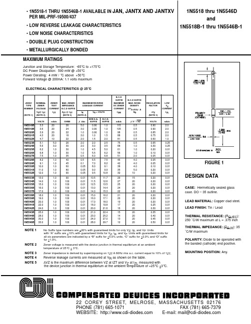
1N5518B-1
JEDEC TYPE NUMBER (NOTE 1)
NOMINAL ZENER VOLTAGE VZ@ 1ZT (NOTE 2) VOLTS
2.0 2.0 2.0 2.0 1.0 0.25 0.25 0.01 0.01 0.01 0.01 0.01 0.01 0.01 0.01 0.01 0.01 0.01 0.01 0.01 0.01 0.01 0.01 0.01 0.01 0.01 0.01 0.01 0.01
FIGURE 1
DESIGN DATA
Junction and Storage Temperature: -65°C to +175°C DC Power Dissipation: 500 mW @ +50°C Power Derating: 4 mW / °C above +50°C Forward Voltage @ 200mA: 1.1 volts maximum ELECTRICAL CHARACTERISTICS @ 25°C
26 24 22 18 22 26 30 30 30 35 40 45 60 80 90 90 100 100 100 100 100 100 100 100 100 100 100 100 100
0.90 0.90 0.90 1.0 1.5 2.0 3.0 4.5 5.5 6.0 6.5 7.0 8.0 9.0 9.5 10.5 11.5 12.5 13.0 14.0 15.0 16.0 17.0 18.0 20.0 21.0 23.0 24.0 28.0
B-C-D SUFFIX MAX. NOISE DENSITY @1Z=250µ A ND
电气工程制图模块七 建筑电气工程图

调光器
(3)常用的插座
三孔插座
五孔插座
带单极开关的(电源)插座
图7-8 常用的插座
2.照明平面图中常用的图形符号 上面我们了解到几种常用的照明电器,在照明平面图中这
些照明电器并没有按照实物的形状来绘制,而是使用图形符号 和文字代号来进行描述,表7-5 列出了照明平面图中常用的布 线方向、插座、开关和灯具的图形符号、名称及说明,这些图 形符号摘自GB/T4728.11—2008《电气简图用图形符号 第11 部分 建筑安装平面布置图》。
图7-1 三层别墅室内装修效果图
1.在日常生活中,我们用到哪些照明电器和用电设 备呢?
2.当要为三层别墅的照明及其他用电设备提供电源 时,应采用什么方法来实现呢 ?
模块七 建筑电气工程图
任务一 别墅照明和动力系统概略图的识读 任务二 别墅照明平面图的识读 任务三 别墅弱电工程图的识读
任务一 别墅照明和动力系统概略图的识读
断路器,
极,额定电流为
,额定剩余动作电流为
。
(4) 首层车库、客厅照明回路N1-BV-2×2.5-PC15-WC的含义是
。
(5) 首层车库、客厅、餐厅插座回路N2-BV-2×4+PE4-PC20-WC的含义是
。
表现要求
评 价
能正确识读线路、配电箱的标注格式
能正确识读别墅首层照明系统概略图
已能达到
未能达到
◆知识要点: 1.熟悉照明和动力系统概略图中常用文字代号的含义; 2.掌握照明和动力系统概略图中线路、配电箱、断路器 的标注格式。 ◆技能要点: 能识读照明和动力概略图。
你知道导线的型号有多种、线径也有所不同吗?你又知道 导线在布线的过程中有哪些常用的方式呢?那么这些内容在建 筑工程图上是如何描述清楚的呢?
- 1、下载文档前请自行甄别文档内容的完整性,平台不提供额外的编辑、内容补充、找答案等附加服务。
- 2、"仅部分预览"的文档,不可在线预览部分如存在完整性等问题,可反馈申请退款(可完整预览的文档不适用该条件!)。
- 3、如文档侵犯您的权益,请联系客服反馈,我们会尽快为您处理(人工客服工作时间:9:00-18:30)。
1N5221B - 1N5267B
500mW EPITAXIAL ZENER DIODE
Features
Maximum Ratings and Electrical Characteristics
@ T A = 25°C unless otherwise specified
·Case: DO-35·Case Material: Glass
·Moisture Sensitivity: Level 1 per J-STD-020C ·Leads: Solderable per MIL-STD-202, Method 208·Terminals: Finish - Sn96.5Ag3.5. Solderable per MIL-STD-202, Method 208·Polarity: Cathode Band ·Marking: Type Number
·
Weight: 0.13 grams (approximate)
·500mW Power Dissipation ·High Stability
·Surface Mount Equivalents Available ·Hermetic Package
·V Z - Tolerance ±5%
·
Lead Free Finish, RoHS Compliant (Note 2)
Mechanical Data
Notes:
1. Valid provided that leads are kept at TL £75°C with lead length = 9.5mm (3/8”) from case; derate above 75°C.
2.EC Directive 2002/95/EC (RoHS) revision 1
3.2.2003. Glass and High Temperature Solder Exemptions Applied where applicable,
see EU Directive Annex Notes 5 and 7.
Electrical Characteristics Table 1
@ T A= 25°C unless otherwise specified
Notes: 3. Based on dc measurement at thermal equilibrium; lead length = 9.5mm (3/8”); thermal resistance of heat sink = 30°C/W.
Ordering Information(Note 5)
Notes: 4. *Add "-A" or "-T" to the appropriate type number in Table 1. Example: 6.2V Zener= 1N5234B-A for ammo pack.
5. For packaging details, visit our website at /datasheets/ap02008.pdf.
IMPORTANT NOTICE
Diodes Incorporated and its subsidiaries reserve the right to make modifications,enhancements,improvements,corrections or other changes without further notice to any product herein.Diodes Incorporated does not assume any liability arising out of the application or use of any product described herein;neither does it convey any license under its patent rights,nor the rights of others.The user of products in such applications shall assume all risks of such use and will agree to hold Diodes Incorporated and all the companies whose products are represented on our website,harmless against all damages.
LIFE SUPPORT
Diodes Incorporated products are not authorized for use as critical components in life support devices or systems without the expressed written approval of the President of Diodes Incorporated.。