M54583FP中文资料
MAX13085EESA-T中文资料

General DescriptionThe MAX13080E–MAX13089E +5.0V, ±15kV ESD-protect-ed, RS-485/RS-422 transceivers feature one driver and one receiver. These devices include fail-safe circuitry,guaranteeing a logic-high receiver output when receiver inputs are open or shorted. The receiver outputs a logic-high if all transmitters on a terminated bus are disabled (high impedance). The MAX13080E–MAX13089E include a hot-swap capability to eliminate false transitions on the bus during power-up or hot insertion.The MAX13080E/MAX13081E/MAX13082E feature reduced slew-rate drivers that minimize EMI and reduce reflections caused by improperly terminated cables, allowing error-free data transmission up to 250kbps. The MAX13083E/MAX13084E/MAX13085E also feature slew-rate-limited drivers but allow transmit speeds up to 500kbps. The MAX13086E/MAX13087E/MAX13088E driver slew rates are not limited, making transmit speeds up to 16Mbps possible. The MAX13089E slew rate is pin selectable for 250kbps,500kbps, and 16Mbps.The MAX13082E/MAX13085E/MAX13088E are intended for half-duplex communications, and the MAX13080E/MAX13081E/MAX13083E/MAX13084E/MAX13086E/MAX13087E are intended for full-duplex communica-tions. The MAX13089E is selectable for half-duplex or full-duplex operation. It also features independently programmable receiver and transmitter output phase through separate pins.The MAX13080E–MAX13089E transceivers draw 1.2mA of supply current when unloaded or when fully loaded with the drivers disabled. All devices have a 1/8-unit load receiver input impedance, allowing up to 256transceivers on the bus.The MAX13080E/MAX13083E/MAX13086E/MAX13089E are available in 14-pin PDIP and 14-pin SO packages.The MAX13081E/MAX13082E/MAX13084E/MAX13085E/MAX13087E/MAX13088E are available in 8-pin PDIP and 8-pin SO packages. The devices operate over the com-mercial, extended, and automotive temperature ranges.ApplicationsUtility Meters Lighting Systems Industrial Control Telecom Security Systems Instrumentation ProfibusFeatures♦+5.0V Operation♦Extended ESD Protection for RS-485/RS-422 I/O Pins±15kV Human Body Model ♦True Fail-Safe Receiver While Maintaining EIA/TIA-485 Compatibility ♦Hot-Swap Input Structures on DE and RE ♦Enhanced Slew-Rate Limiting Facilitates Error-Free Data Transmission(MAX13080E–MAX13085E/MAX13089E)♦Low-Current Shutdown Mode (Except MAX13081E/MAX13084E/MAX13087E)♦Pin-Selectable Full-/Half-Duplex Operation (MAX13089E)♦Phase Controls to Correct for Twisted-Pair Reversal (MAX13089E)♦Allow Up to 256 Transceivers on the Bus ♦Available in Industry-Standard 8-Pin SO PackageMAX13080E–MAX13089E+5.0V , ±15kV ESD-Protected, Fail-Safe, Hot-Swap, RS-485/RS-422 Transceivers________________________________________________________________Maxim Integrated Products 1Ordering Information19-3590; Rev 1; 4/05For pricing, delivery, and ordering information,please contact Maxim/Dallas Direct!at 1-888-629-4642, or visit Maxim’s website at .Selector Guide, Pin Configurations, and Typical Operating Circuits appear at end of data sheet.Ordering Information continued at end of data sheet.M A X 13080E –M A X 13089E+5.0V , ±15kV ESD-Protected, Fail-Safe, Hot-Swap, RS-485/RS-422 Transceivers 2_______________________________________________________________________________________ABSOLUTE MAXIMUM RATINGSDC ELECTRICAL CHARACTERISTICS(V CC = +5.0V ±10%, T A = T MIN to T MAX , unless otherwise noted. Typical values are at V CC = +5.0V and T A = +25°C.) (Note 1)Stresses beyond those listed under “Absolute Maximum Ratings” may cause permanent damage to the device. These are stress ratings only, and functional operation of the device at these or any other conditions beyond those indicated in the operational sections of the specifications is not implied. Exposure to absolute maximum rating conditions for extended periods may affect device reliability.(All Voltages Referenced to GND)Supply Voltage (V CC ).............................................................+6V Control Input Voltage (RE , DE, SLR,H/F , TXP, RXP)......................................................-0.3V to +6V Driver Input Voltage (DI)...........................................-0.3V to +6V Driver Output Voltage (Z, Y, A, B).............................-8V to +13V Receiver Input Voltage (A, B)....................................-8V to +13V Receiver Input VoltageFull Duplex (A, B)..................................................-8V to +13V Receiver Output Voltage (RO)....................-0.3V to (V CC + 0.3V)Driver Output Current.....................................................±250mAContinuous Power Dissipation (T A = +70°C)8-Pin SO (derate 5.88mW/°C above +70°C).................471mW 8-Pin Plastic DIP (derate 9.09mW/°C above +70°C).....727mW 14-Pin SO (derate 8.33mW/°C above +70°C)...............667mW 14-Pin Plastic DIP (derate 10.0mW/°C above +70°C)...800mW Operating Temperature RangesMAX1308_EC_ _.................................................0°C to +75°C MAX1308_EE_ _..............................................-40°C to +85°C MAX1308_EA_ _............................................-40°C to +125°C Junction Temperature......................................................+150°C Storage Temperature Range.............................-65°C to +150°C Lead Temperature (soldering, 10s).................................+300°CMAX13080E–MAX13089E+5.0V , ±15kV ESD-Protected, Fail-Safe, Hot-Swap, RS-485/RS-422 Transceivers_______________________________________________________________________________________3DC ELECTRICAL CHARACTERISTICS (continued)(V CC = +5.0V ±10%, T A = T MIN to T MAX , unless otherwise noted. Typical values are at V CC = +5.0V and T A = +25°C.) (Note 1)M A X 13080E –M A X 13089E+5.0V , ±15kV ESD-Protected, Fail-Safe, Hot-Swap, RS-485/RS-422 Transceivers 4_______________________________________________________________________________________DRIVER SWITCHING CHARACTERISTICSMAX13080E/MAX13081E/MAX13082E/MAX13089E WITH SRL = UNCONNECTED (250kbps)(V CC = +5.0V ±10%, T A = T MIN to T MAX , unless otherwise noted. Typical values are at V CC = +5.0V and T A = +25°C.)RECEIVER SWITCHING CHARACTERISTICSMAX13080E/MAX13081E/MAX13082E/MAX13089E WITH SRL = UNCONNECTED (250kbps)(V CC = +5.0V ±10%, T A = T MIN to T MAX , unless otherwise noted. Typical values are at V CC = +5.0V and T A = +25°C.)MAX13080E–MAX13089E+5.0V , ±15kV ESD-Protected, Fail-Safe, Hot-Swap, RS-485/RS-422 Transceivers_______________________________________________________________________________________5DRIVER SWITCHING CHARACTERISTICSMAX13083E/MAX13084E/MAX13085E/MAX13089E WITH SRL = V CC (500kbps)(V CC = +5.0V ±10%, T A = T MIN to T MAX , unless otherwise noted. Typical values are at V CC = +5.0V and T A = +25°C.)RECEIVER SWITCHING CHARACTERISTICSMAX13083E/MAX13084E/MAX13085E/MAX13089E WITH SRL = V CC (500kbps)(V CC = +5.0V ±10%, T A = T MIN to T MAX , unless otherwise noted. Typical values are at V CC = +5.0V and T A = +25°C.)M A X 13080E –M A X 13089E+5.0V , ±15kV ESD-Protected, Fail-Safe, Hot-Swap, RS-485/RS-422 Transceivers 6_______________________________________________________________________________________DRIVER SWITCHING CHARACTERISTICSMAX13086E/MAX13087E/MAX13088E/MAX13089E WITH SRL = GND (16Mbps)(V CC = +5.0V ±10%, T A = T MIN to T MAX , unless otherwise noted. Typical values are at V CC = +5.0V and T A = +25°C.)RECEIVER SWITCHING CHARACTERISTICSMAX13086E/MAX13087E/MAX13088E/MAX13089E WITH SRL = GND (16Mbps)(V CC = +5.0V ±10%, T A = T MIN to T MAX , unless otherwise noted. Typical values are at V CC = +5.0V and T A = +25°C.)Note 2:∆V OD and ∆V OC are the changes in V OD and V OC , respectively, when the DI input changes state.Note 3:The short-circuit output current applies to peak current just prior to foldback current limiting. The short-circuit foldback outputcurrent applies during current limiting to allow a recovery from bus contention.MAX13080E–MAX13089E+5.0V , ±15kV ESD-Protected, Fail-Safe, Hot-Swap, RS-485/RS-422 Transceivers_______________________________________________________________________________________70.800.901.501.101.001.201.301.401.60-40-10520-253550958011065125SUPPLY CURRENT vs. TEMPERATURETEMPERATURE (°C)S U P P L Y C U R R E N T (m A )0201040305060021345OUTPUT CURRENTvs. RECEIVER OUTPUT-HIGH VOLTAGEM A X 13080E -89E t o c 02OUTPUT HIGH VOLTAGE (V)O U T P U T C U R R E N T (m A )20104030605070021345OUTPUT CURRENTvs. RECEIVER OUTPUT-LOW VOLTAGEM A X 13080E -89E t o c 03OUTPUT LOW VOLTAGE (V)O U T P U T C U R R E N T (m A )4.04.44.24.84.65.25.05.4RECEIVER OUTPUT-HIGH VOLTAGEvs. TEMPERATURETEMPERATURE (°C)O U T P U T H I G H V O L T A G E (V )-40-10520-2535509580110651250.10.70.30.20.40.50.60.8RECEIVER OUTPUT-LOW VOLTAGEvs. TEMPERATURETEMPERATURE (°C)O U T P U T L O W V O L T A G E (V )-40-10520-25355095801106512502040608010012014016012345DRIVER DIFFERENTIAL OUTPUT CURRENT vs. DIFFERENTIAL OUTPUT VOLTAGEDIFFERENTIAL OUTPUT VOLTAGE (V)D I F FE R E N T I A L O U T P U T C U R R E N T (m A )2.02.82.43.63.24.44.04.8DRIVER DIFFERENTIAL OUTPUT VOLTAGE vs. TEMPERATURED I F FE R E N T I A L O U T P U T V O L T A G E (V )-40-10520-253550958011065125TEMPERATURE (°C)40201008060120140180160200-7-5-4-6-3-2-1012354OUTPUT CURRENT vs. TRANSMITTEROUTPUT-HIGH VOLTAGEOUTPUT HIGH VOLTAGE (V)O U T P U T C U R R E N T (m A )60402080100120140160180200042681012OUTPUT CURRENT vs. TRANSMITTEROUTPUT-LOW VOLTAGEOUTPUT-LOW VOLTAGE (V)O U T P U T C U R R E N T (m A )Typical Operating Characteristics(V CC = +5.0V, T A = +25°C, unless otherwise noted.)M A X 13080E –M A X 13089E+5.0V , ±15kV ESD-Protected, Fail-Safe, Hot-Swap, RS-485/RS-422 Transceivers 8_______________________________________________________________________________________21543679810SHUTDOWN CURRENT vs. TEMPERATUREM A X 13080E -89E t o c 10S H U T D O W N C U R R E N T (µA )-40-10520-253550958011065125TEMPERATURE (°C)600800700100090011001200DRIVER PROPAGATION DELAY vs. TEMPERATURE (250kbps)D R I VE R P R O P A G A T I O N D E L A Y (n s )-40-10520-253550958011065125TEMPERATURE (°C)300400350500450550600DRIVER PROPAGATION DELAY vs. TEMPERATURE (500kbps)D R I VE R P R O P A G A T I O N D E L A Y (n s )-40-10520-253550958011065125TEMPERATURE (°C)1070302040506080DRIVER PROPAGATION DELAY vs. TEMPERATURE (16Mbps)D R I VE R P R O P A G A T I O N D E L A Y (n s )-40-10520-253550958011065125TEMPERATURE (°C)40201008060120140160180RECEIVER PROPAGATION DELAYvs. TEMPERATURE (250kpbs AND 500kbps)R E C E I V E R P R O P A G A T I O N D E L A Y (n s )-40-10520-253550958011065125TEMPERATURE (°C)40201008060120140160180RECEIVER PROPAGATION DELAYvs. TEMPERATURE (16Mbps)R EC E I V E R P R O P A G AT I O N D E L A Y (n s )-40-10520-253550958011065125TEMPERATURE (°C)2µs/div DRIVER PROPAGATION DELAY (250kbps)DI 2V/divV Y - V Z 5V/divR L = 100Ω200ns/divRECEIVER PROPAGATION DELAY(250kbps AND 500kbps)V A - V B 5V/divRO 2V/divTypical Operating Characteristics (continued)(V CC = +5.0V, T A = +25°C, unless otherwise noted.)MAX13080E–MAX13089E+5.0V , ±15kV ESD-Protected, Fail-Safe, Hot-Swap, RS-485/RS-422 Transceivers_______________________________________________________________________________________9Test Circuits and Waveforms400ns/divDRIVER PROPAGATION DELAY (500kbps)DI 2V/divR L = 100ΩV Y - V Z 5V/div10ns/div DRIVER PROPAGATION DELAY (16Mbps)DI 2V/divR L = 100ΩV Y 2V/divV Z 2V/div40ns/divRECEIVER PROPAGATION DELAY (16Mbps)V B 2V/divR L = 100ΩRO 2V/divV A 2V/divTypical Operating Characteristics (continued)(V CC = +5.0V, T A = +25°C, unless otherwise noted.)Figure 2. Driver Timing Test CircuitM A X 13080E –M A X 13089E+5.0V , ±15kV ESD-Protected, Fail-Safe, Hot-Swap, RS-485/RS-422 Transceivers 10______________________________________________________________________________________Test Circuits and Waveforms (continued)Figure 4. Driver Enable and Disable Times (t DHZ , t DZH , t DZH(SHDN))DZL DLZ DLZ(SHDN)MAX13080E–MAX13089E+5.0V , ±15kV ESD-Protected, Fail-Safe, Hot-Swap, RS-485/RS-422 TransceiversTest Circuits and Waveforms (continued)Figure 6. Receiver Propagation Delay Test CircuitM A X 13080E –M A X 13089E+5.0V , ±15kV ESD-Protected, Fail-Safe, Hot-Swap, RS-485/RS-422 TransceiversMAX13080E–MAX13089E+5.0V , ±15kV ESD-Protected, Fail-Safe, Hot-Swap, RS-485/RS-422 TransceiversMAX13080E/MAX13083E/MAX13086EMAX13081E/MAX13084E/MAX13086E/MAX13087EFunction TablesM A X 13080E –M A X 13089E+5.0V , ±15kV ESD-Protected, Fail-Safe, Hot-Swap, RS-485/RS-422 Transceivers MAX13082E/MAX13085E/MAX13088EFunction Tables (continued)MAX13089EDetailed Description The MAX13080E–MAX13089E high-speed transceivers for RS-485/RS-422 communication contain one driver and one receiver. These devices feature fail-safe circuit-ry, which guarantees a logic-high receiver output when the receiver inputs are open or shorted, or when they are connected to a terminated transmission line with all dri-vers disabled (see the Fail-Safe section). The MAX13080E/MAX13082E/MAX13083E/MAX13085E/ MAX13086E/MAX13088E/MAX13089E also feature a hot-swap capability allowing line insertion without erroneous data transfer (see the Hot Swap Capability section). The MAX13080E/MAX13081E/MAX13082E feature reduced slew-rate drivers that minimize EMI and reduce reflec-tions caused by improperly terminated cables, allowing error-free data transmission up to 250kbps. The MAX13083E/MAX13084E/MAX13085E also offer slew-rate limits allowing transmit speeds up to 500kbps. The MAX13086E/MAX13087E/MAX13088Es’ driver slew rates are not limited, making transmit speeds up to 16Mbps possible. The MAX13089E’s slew rate is selectable between 250kbps, 500kbps, and 16Mbps by driving a selector pin with a three-state driver.The MAX13082E/MAX13085E/MAX13088E are half-duplex transceivers, while the MAX13080E/MAX13081E/ MAX13083E/MAX13084E/MAX13086E/MAX13087E are full-duplex transceivers. The MAX13089E is selectable between half- and full-duplex communication by driving a selector pin (H/F) high or low, respectively.All devices operate from a single +5.0V supply. Drivers are output short-circuit current limited. Thermal-shutdown circuitry protects drivers against excessive power dissi-pation. When activated, the thermal-shutdown circuitry places the driver outputs into a high-impedance state.Receiver Input Filtering The receivers of the MAX13080E–MAX13085E, and the MAX13089E when operating in 250kbps or 500kbps mode, incorporate input filtering in addition to input hysteresis. This filtering enhances noise immunity with differential signals that have very slow rise and fall times. Receiver propagation delay increases by 25% due to this filtering.Fail-Safe The MAX13080E family guarantees a logic-high receiver output when the receiver inputs are shorted or open, or when they are connected to a terminated transmission line with all drivers disabled. This is done by setting the receiver input threshold between -50mV and -200mV. If the differential receiver input voltage (A - B) is greater than or equal to -50mV, RO is logic-high. If (A - B) is less than or equal to -200mV, RO is logic-low. In the case of a terminated bus with all transmitters disabled, the receiv-er’s differential input voltage is pulled to 0V by the termi-nation. With the receiver thresholds of the MAX13080E family, this results in a logic-high with a 50mV minimumnoise margin. Unlike previous fail-safe devices, the-50mV to -200mV threshold complies with the ±200mVEIA/TIA-485 standard.Hot-Swap Capability (Except MAX13081E/MAX13084E/MAX13087E)Hot-Swap InputsWhen circuit boards are inserted into a hot or powered backplane, differential disturbances to the data buscan lead to data errors. Upon initial circuit board inser-tion, the data communication processor undergoes itsown power-up sequence. During this period, the processor’s logic-output drivers are high impedanceand are unable to drive the DE and RE inputs of these devices to a defined logic level. Leakage currents up to±10µA from the high-impedance state of the proces-sor’s logic drivers could cause standard CMOS enableinputs of a transceiver to drift to an incorrect logic level. Additionally, parasitic circuit board capacitance couldcause coupling of V CC or GND to the enable inputs. Without the hot-swap capability, these factors could improperly enable the transceiver’s driver or receiver.When V CC rises, an internal pulldown circuit holds DElow and RE high. After the initial power-up sequence,the pulldown circuit becomes transparent, resetting thehot-swap tolerable input.Hot-Swap Input CircuitryThe enable inputs feature hot-swap capability. At theinput there are two NMOS devices, M1 and M2 (Figure 9). When V CC ramps from zero, an internal 7µstimer turns on M2 and sets the SR latch, which alsoturns on M1. Transistors M2, a 1.5mA current sink, andM1, a 500µA current sink, pull DE to GND through a5kΩresistor. M2 is designed to pull DE to the disabledstate against an external parasitic capacitance up to100pF that can drive DE high. After 7µs, the timer deactivates M2 while M1 remains on, holding DE low against three-state leakages that can drive DE high. M1 remains on until an external source overcomes the required input current. At this time, the SR latch resetsand M1 turns off. When M1 turns off, DE reverts to a standard, high-impedance CMOS input. Whenever V CCdrops below 1V, the hot-swap input is reset.For RE there is a complementary circuit employing two PMOS devices pulling RE to V CC. MAX13080E–MAX13089E+5.0V, ±15kV ESD-Protected, Fail-Safe, Hot-Swap, RS-485/RS-422 TransceiversM A X 13080E –M A X 13089EMAX13089E ProgrammingThe MAX13089E has several programmable operating modes. Transmitter rise and fall times are programma-ble, resulting in maximum data rates of 250kbps,500kbps, and 16Mbps. To select the desired data rate,drive SRL to one of three possible states by using a three-state driver: V CC , GND, or unconnected. F or 250kbps operation, set the three-state device in high-impedance mode or leave SRL unconnected. F or 500kbps operation, drive SRL high or connect it to V CC .F or 16Mbps operation, drive SRL low or connect it to GND. SRL can be changed during operation without interrupting data communications.Occasionally, twisted-pair lines are connected backward from normal orientation. The MAX13089E has two pins that invert the phase of the driver and the receiver to cor-rect this problem. F or normal operation, drive TXP and RXP low, connect them to ground, or leave them uncon-nected (internal pulldown). To invert the driver phase,drive TXP high or connect it to V CC . To invert the receiver phase, drive RXP high or connect it to V CC . Note that the receiver threshold is positive when RXP is high.The MAX13089E can operate in full- or half-duplex mode. Drive H/F low, leave it unconnected (internal pulldown), or connect it to GND for full-duplex opera-tion. Drive H/F high for half-duplex operation. In full-duplex mode, the pin configuration of the driver and receiver is the same as that of a MAX13080E. In half-duplex mode, the receiver inputs are internally connect-ed to the driver outputs through a resistor-divider. This effectively changes the function of the device’s outputs.Y becomes the noninverting driver output and receiver input, Z becomes the inverting driver output and receiver input. In half-duplex mode, A and B are still connected to ground through an internal resistor-divider but they are not internally connected to the receiver.±15kV ESD ProtectionAs with all Maxim devices, ESD-protection structures are incorporated on all pins to protect against electro-static discharges encountered during handling and assembly. The driver outputs and receiver inputs of the MAX13080E family of devices have extra protection against static electricity. Maxim’s engineers have devel-oped state-of-the-art structures to protect these pins against ESD of ±15kV without damage. The ESD struc-tures withstand high ESD in all states: normal operation,shutdown, and powered down. After an ESD event, the MAX13080E–MAX13089E keep working without latchup or damage.ESD protection can be tested in various ways. The transmitter outputs and receiver inputs of the MAX13080E–MAX13089E are characterized for protec-tion to the following limits:•±15kV using the Human Body Model•±6kV using the Contact Discharge method specified in IEC 61000-4-2ESD Test ConditionsESD performance depends on a variety of conditions.Contact Maxim for a reliability report that documents test setup, test methodology, and test results.Human Body ModelFigure 10a shows the Human Body Model, and Figure 10b shows the current waveform it generates when dis-charged into a low impedance. This model consists of a 100pF capacitor charged to the ESD voltage of interest,which is then discharged into the test device through a 1.5k Ωresistor.IEC 61000-4-2The IEC 61000-4-2 standard covers ESD testing and performance of finished equipment. However, it does not specifically refer to integrated circuits. The MAX13080E family of devices helps you design equip-ment to meet IEC 61000-4-2, without the need for addi-tional ESD-protection components.+5.0V , ±15kV ESD-Protected, Fail-Safe, Hot-Swap, RS-485/RS-422 TransceiversThe major difference between tests done using the Human Body Model and IEC 61000-4-2 is higher peak current in IEC 61000-4-2 because series resistance is lower in the IEC 61000-4-2 model. Hence, the ESD with-stand voltage measured to IEC 61000-4-2 is generally lower than that measured using the Human Body Model. Figure 10c shows the IEC 61000-4-2 model, and Figure 10d shows the current waveform for IEC 61000-4-2 ESD Contact Discharge test.Machine Model The machine model for ESD tests all pins using a 200pF storage capacitor and zero discharge resis-tance. The objective is to emulate the stress caused when I/O pins are contacted by handling equipment during test and assembly. Of course, all pins require this protection, not just RS-485 inputs and outputs.Applications Information256 Transceivers on the BusThe standard RS-485 receiver input impedance is 12kΩ(1-unit load), and the standard driver can drive up to 32-unit loads. The MAX13080E family of transceivers has a1/8-unit load receiver input impedance (96kΩ), allowingup to 256 transceivers to be connected in parallel on one communication line. Any combination of these devices,as well as other RS-485 transceivers with a total of 32-unit loads or fewer, can be connected to the line.Reduced EMI and ReflectionsThe MAX13080E/MAX13081E/MAX13082E feature reduced slew-rate drivers that minimize EMI and reduce reflections caused by improperly terminated cables, allowing error-free data transmission up to250kbps. The MAX13083E/MAX13084E/MAX13085Eoffer higher driver output slew-rate limits, allowing transmit speeds up to 500kbps. The MAX13089E withSRL = V CC or unconnected are slew-rate limited. WithSRL unconnected, the MAX13089E error-free data transmission is up to 250kbps. With SRL connected toV CC,the data transmit speeds up to 500kbps. MAX13080E–MAX13089E+5.0V, ±15kV ESD-Protected, Fail-Safe, Hot-Swap, RS-485/RS-422 TransceiversM A X 13080E –M A X 13089ELow-Power Shutdown Mode (Except MAX13081E/MAX13084E/MAX13087E)Low-power shutdown mode is initiated by bringing both RE high and DE low. In shutdown, the devices typically draw only 2.8µA of supply current.RE and DE can be driven simultaneously; the devices are guaranteed not to enter shutdown if RE is high and DE is low for less than 50ns. If the inputs are in this state for at least 700ns, the devices are guaranteed to enter shutdown.Enable times t ZH and t ZL (see the Switching Characteristics section) assume the devices were not in a low-power shutdown state. Enable times t ZH(SHDN)and t ZL(SHDN)assume the devices were in shutdown state. It takes drivers and receivers longer to become enabled from low-power shutdown mode (t ZH(SHDN), t ZL(SHDN))than from driver/receiver-disable mode (t ZH , t ZL ).Driver Output ProtectionTwo mechanisms prevent excessive output current and power dissipation caused by faults or by bus contention.The first, a foldback current limit on the output stage,provides immediate protection against short circuits over the whole common-mode voltage range (see the Typical Operating Characteristics ). The second, a thermal-shut-down circuit, forces the driver outputs into a high-imped-ance state if the die temperature exceeds +175°C (typ).Line LengthThe RS-485/RS-422 standard covers line lengths up to 4000ft. F or line lengths greater than 4000ft, use the repeater application shown in Figure 11.Typical ApplicationsThe MAX13082E/MAX13085E/MAX13088E/MAX13089E transceivers are designed for bidirectional data commu-nications on multipoint bus transmission lines. F igures 12 and 13 show typical network applications circuits. To minimize reflections, terminate the line at both ends in its characteristic impedance, and keep stub lengths off the main line as short as possible. The slew-rate-lim-ited MAX13082E/MAX13085E and the two modes of the MAX13089E are more tolerant of imperfect termination.Chip InformationTRANSISTOR COUNT: 1228PROCESS: BiCMOS+5.0V , ±15kV ESD-Protected, Fail-Safe, Hot-Swap, RS-485/RS-422 TransceiversFigure 11. Line Repeater for MAX13080E/MAX13081E/MAX13083E/MAX13084E/MAX13086E/MAX13087E/MAX13089E in Full-Duplex Mode+5.0V, ±15kV ESD-Protected, Fail-Safe, Hot-Swap, RS-485/RS-422 TransceiversMAX13080E–MAX13089EM A X 13080E –M A X 13089E+5.0V , ±15kV ESD-Protected, Fail-Safe, Hot-Swap, RS-485/RS-422 TransceiversPin Configurations and Typical Operating CircuitsMAX13080E–MAX13089E+5.0V , ±15kV ESD-Protected, Fail-Safe, Hot-Swap, RS-485/RS-422 Transceivers______________________________________________________________________________________21Pin Configurations and Typical Operating Circuits (continued)M A X 13080E –M A X 13089E+5.0V , ±15kV ESD-Protected, Fail-Safe, Hot-Swap, RS-485/RS-422 Transceivers 22______________________________________________________________________________________Ordering Information (continued)MAX13080E–MAX13089E+5.0V , ±15kV ESD-Protected, Fail-Safe, Hot-Swap, RS-485/RS-422 Transceivers______________________________________________________________________________________23Package Information (continued)(The package drawing(s) in this data sheet may not reflect the most current specifications. For the latest package outline information,go to /packages .)。
M54543L中文资料

VCC=VCC'=12V
V
VOL (2) IIH (1) IIH (2)
"L" Output saturation voltage (2) "H" Input current (1) "H" Input current (2)
VCC=VCC'=12V
VI2=0V VI1=VI2=2V
V µA µA
VCC=VCC'=12V, VI1=2V, VI2=0V VCC=VCC'=12V, VI1=0V, VI2=2V VI1=2V, VI2=0V VCC=VCC' =16V Output open VI1=0V, VI2=2V VI1=VI2=2V VI1=VI2=0V
元器件交易网
MITSUBISHI ICs (AV COMMON)
M54543L
Bi-DIRECTIONAL MOTOR DRIVER WITH BRAKE FUNCTION
DESCRIPTION
The M54543L is a semiconductor IC capable of directly driving a smallsize bi-directional motor for forward/reverse rotation.
Unit µA V V
VI2=0V VI1=0V VI2=2V VI1=0V VI2=2V VI1=VI2=2V VI1=2V
VCC=VCC'=12V
IOL (1)=300mA IOL (1)=500mA IOL (2)=300mA IOL (2)=500mA
VOL (1)
"L" Output saturation voltage (1)
M61084FP资料

DESCRIPTIONThe M61084FP is a semiconductor integrated circuit developed for DVD and CD-ROM (8 timesspeed) players. The IC is housed in a 12-pin clear molded plastic package and contains 8preamplifiers with divided photodetectors.FEATURES Array• 8 amplifiers with divided photodetectors• Using small package ( 5.0X4.0X1.5 mm )• For differential push-pull techniqueand single beam phase difference technique• High Band preamplifier circuit (DC-20MHz)• For red reys laser diode (ex. =635 nm) ArrayAPPLICATIONDVD , CD-ROM etc.RECOMMENDED OPERATING CONDITIONSSupply voltage • • • • • • • • • • 4.5V to 5.5VRated supply voltage • • • • • • 5.0VTEST CIRCUIT005010015020025025507510012570300THERMAL DERATING (MAXIMUM RATINGS)AMBIENT TEMPERATURE Ta (˚C)ABSOLUTE MAXIMUM RATINGS (Ta=25˚C,unless otherwise noted)*Please set the condenser connected to Vcc and Vc near the pin. (Within 10mm)Units Resistance : ΩCapacitance : FTest conditions Min Typ Max Unit In the darkPo=10µW =635nmOutput A to D without offset voltagePo=10µW =635nmOutput E to H without offset voltage In the dark (A+B) - (C+D)In the dark (A+D) - (B+C)In the dark E - F In the dark Output A to H3.5 5.0 6.5210270330400500600-150+15-150+15-150+15-150+15Limits mA mV mV mVmVParameter Circuit currentOutput voltageOutput offset voltageDelta output offset voltageFrequency characteristicOutput noise voltagePo=10µW/cell =635nm30%modulation 3 dB down Output A to DPo=10µW/cell =635nm 30%modulation 3 dBdown Output E to HOutput A to D (at f=5MHz)1520-1.0 1.5---80-74MHzdBmSymbolIccVo V ∆VOFFfcVNOELECTRICAL CHARACTERISTICS (VCC=5.0V,Ta=25˚C,unless otherwise noted)In the dark G - H-150+15VOMAXMaximum Output voltageOutput A to H maximum voltageat Vcc=5.0 v 3.5--VOptical sensitivity on SPD=635nm Output A to H-0.3-A/WOFF RYXPD SIZE (TYPICAL)YXNote )A public difference from the SPD center and the flame0.2mm A public difference from the center of the flame of molded package0.2mm A public difference from the center of SPD and the center of molded package0.4mm The rotation deviation of SPD toward the flame3 degree++++。
M5840-V2.0规格书(中文)
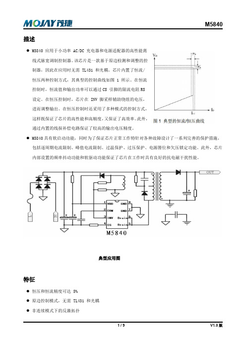
恒流工作
M5840 的恒压/恒流特征曲线如图 1 所示。M5840 被设计应用于工作在非连续模式下的反激式系统中。
在正常工作时,当 INV 电压低于内部 2.0V 的基准电压好时,系统工作在恒流模式,否则系统工作在恒压
模式。当次级输出电流达到了系统设定的最大电流时,系统就进入恒流模式,并且会引起输出电压的下降。
电气参数 (Ta=25oC, 其余情况会做说明)
(如无特殊说明, VIN=12V(注 1), TA=25℃)
参数
启动电流
工作电流
进入欠压锁定的阈值电压 退出欠压锁定的阈值电压 过压保护的阈值电压 电源箝位电压 内置 MOS 管耐压值 MOS 管导通电阻值 前沿消隐时间 过流保护阈值 过流保护延迟 输入阻抗 软启动时间 正常工作频率 启动频率 频率抖动幅度 误差放大器的输入基准电压 误差放大器的直流增益 线损补偿最大电流 输出低电平
由于 TDemag 与电感的大小成反比,因此,电感 LP 和 FSW 的乘积为一定值,从而限制了最大的输 出功率,避免了系统进入连续工作模式。
电流检测和前沿消隐 M5840 采样功率 MOSFET 上的电流是通过 CS 来实现的。 M5840 不仅设计了逐周期的电流限制,而
且设计了峰值电流限制,最大的峰值电流电压为 0.9V。因此,MOSFET 上最大的峰值电流为:
随着输出电压的下降,反馈电压也跟着下降,芯片内部的 VCO 将
会调整开关的频率,以使输出功率保持和输出电压成正比,其结
果就是使输出电流保持恒定。这就是恒流的原理。在恒流模式下,
无论输出电压如何变化,输出电流为一常数。在作为充电器应用
时,先是恒流充电直到接近电池充饱的状态,随后再进行恒压充
电。在 M5840 中, 恒流值和最大输出功率可以通过外部的限流
M30626FHPFP中文资料
Rev.2.10 Nov. 07, 2003 page 1 of 84
元器件交易网
M16C/62 Group (M16C/62P, M16C/62PT)
1. Overview
1.2 Performance Outline
Table 1.1 to table 1.3 list performance outline of M16C/62 group (M16C/62P, M16C/62PT). Table 1.1 Performance outline of M16C/62 group (M16C/62P) (128-pin version)
Item
CPU
Number of basic instructions Shortest instruction execution time
Operation mode Memory space
Peripheral function
Memory capacity Port Multifunction timer
memory space expansion function)
Memory capacity
See table 1.4 to 1.7 Product List
Peripheral Port
Input/Output : 87 pins, Input : 1pin
function
Multifunction timer
Serial I/O
A-D converter D-A converter DMAC CRC calculation circuit Watchdog timer Interrupt
Clock generating circuit
M50436-560SP

一台黄河18彩电,故障现象是,无屏显,面板和遥控器都只可以调节频道上下翻看,其余全部失效。
先修理屏显电路。经检查,发现同步信号引入电路的两个二极管VD708和VD709都损坏,全开路。更换好后屏显出来了,显示内容是频道预调状态。此种CPU在预调状态下的确只能够调节频道加减和节目号编辑,其余的不能控制。再检查预调开关,已经卡死。更换后,电视机恢复正常。
一台泰山牌TS49C11型普通遥控彩电,记忆功能均失效。
本机主板采用松下M11机心电路,遥控部分采用三菱公司的遥控系统,CPU(M50436-560SP)内不含存储器,各种信息数据均由存储器N902(M58655P)来承担。
N902{1}脚为+5V电源输入端;{2}脚为-30V电源输入端;{7}、{8}、{9}脚为工作方式选择(读、写、清除)输入端,它们分别接受CPU{31}、{32}、{33}脚输出信号的控制;{12}脚为数据输入/输出端。
用M58C655(或CM58655)更换M58655P时,只需将M58C655(或CM58655){2}脚悬空或翘起,其余引脚对应插入N902的位置焊接即可。
据故障现象分析,首先检查N902的工作电源电压是否正常。测其{1}脚电源+5V正常,而{2}脚电压却为0V。查{2}脚供电电路上的元件,发现-30V稳压二极管V920(IN941)短路损坏(见附图),{2}脚无-30V写片电源,而出现上述故障现象。用同型号件更换V920,开机搜索,记忆功能恢复正常,交用户使用。谁知第二天用户又返修,其故障与上次相同。端电压,随着时间的推移,发现该电压会逐渐升高,当升至-39V以上时,V920就击穿。笔者最初认为这些更换的元件质量有问题,怀疑其稳压性能变差所致。于是购回多种型号的-30V稳压二极管来逐一进行更换,但使用不久仍屡击穿。检修工作陷入困境。
HK32F030MxxxxA HK32F0301MxxxxA 数据手册说明书

HK32F030MxxxxA/HK32F0301MxxxxA数据手册版本:1.3发布日期:2022-11-22深圳市航顺芯片技术研发有限公司前言前言编写目的本文档介绍了HK32F030MxxxxA/HK32F0301MxxxxA系列芯片的结构框图、存储器映射、外设接口、电气特性、管脚封装等,旨在帮助用户快速了解该系列芯片的特点及功能。
读者对象本文适用于以下读者:•开发工程师•芯片测试工程师•芯片选型工程师版本说明本文档对应的产品系列为HK32F030MxxxxA/HK32F0301MxxxxA系列芯片。
修订记录目录1 简介 (1)2 产品概述 (3)2.1 产品特性 (3)2.2 器件一览表 (5)3 功能介绍 (8)3.1 结构框图 (8)3.2 存储器映射 (8)3.3 存储器 (9)3.3.1 Flash (9)3.3.2 内置SRAM (9)3.3.3 EEPROM (9)3.4 CRC计算单元 (9)3.5 供电方案 (10)3.6 电源监控器 (10)3.7 低功耗模式 (10)3.8 IO保持 (10)3.9 STBAWU定时器 (10)3.10 复位 (10)3.10.1 系统复位 (11)3.10.2 电源复位 (11)3.11 时钟和时钟树 (11)3.12 SYSCFG (13)3.13 GPIO (13)3.14 引脚选择功能(IOMUX) (13)3.15 中断与事件 (14)3.15.1 NVIC (14)3.15.2 System Tick定时器 (14)3.15.3 EXTI (14)3.16 ADC (14)3.16.1 AWD唤醒功能 (15)3.17 定时器 (15)3.17.1 高级定时器 (15)3.17.2 通用定时器 (15)3.17.3 基本定时器 (16)3.18 AWUT定时器 (16)3.19 独立看门狗(IWDG) (16)3.20 窗口看门狗(WWDG) (16)3.21 I2C总线 (16)3.22 通用同步/异步收发器(USART/UART) (17)3.23 串行外设接口(SPI/I2S) (17)3.24 蜂鸣器(Beeper) (18)3.25 64位UID (18)3.26 调试接口 (18)4 电气性能指标 (19)4.1 最大绝对额定值 (19)4.1.1 极限电压特性 (19)4.1.2 极限电流特性 (19)4.1.3 极限温度特性 (19)4.2 工作参数 (20)4.2.1 推荐工作条件 (20)4.2.2 上/下电复位特性 (20)4.2.3 内部参考电压 (21)4.2.4 工作电流特性 (21)4.2.5 内部高速(HSI)时钟特性 (21)4.2.6 内部低速(LSI)时钟特性 (22)4.2.7 外部时钟输入特性 (22)4.2.8 EEPROM存储器特性 (22)4.2.9 Flash存储器特性 (23)4.2.10 IO输入引脚特性 (23)4.2.11 IO输出引脚特性 (23)4.2.12 NRST复位管脚特性 (24)4.2.13 TIM计数器特性 (24)4.2.14 ADC特性 (24)5 典型电路 (27)5.1 电源供电 (27)6 管脚定义 (28)6.1 SOP8封装 (28)6.2 TSSOP16封装 (29)6.3 TSSOP20封装 (30)6.4 TSSOP24封装 (31)6.5 TSSOP28封装 (32)6.6 QFN20封装 (33)6.7 QFN24封装 (34)6.8 QFN28封装 (35)6.9 各封装的管脚定义 (35)6.10 多引脚选择(IOMUX) (40)6.10.1 SOP8封装的IOMUX映射 (40)6.10.2 TSSOP16封装的IOMUX映射 (43)6.11 引脚复用(AF)功能表 (45)7 封装参数 (47)7.1 SOP8封装 (47)7.2 TSSOP16封装 (48)7.3 TSSOP20封装 (49)7.4 TSSOP24封装 (50)7.5 TSSOP28封装 (52)7.6 QFN20封装 (53)7.7 QFN24封装 (56)7.8 QFN28封装 (56)8 订货信息 (59)9 缩略语 (61)10 重要提示 (63)1简介本文档为HK32F030MxxxxA及HK32F0301MxxxxA系列芯片的数据手册。
HK32F030M 数据手册说明书

HK32F030M 数据手册Rev1.0.12ContentsHistory (5)1说明 (6)2产品综述 (7)2.1产品简介 (7)2.2产品特点 (8)2.3器件一览表 (9)2.4订货代码 (10)3功能介绍 (11)3.1结构框图 (11)3.2存储器映射 (12)3.2.1Flash特性 (12)3.2.2Flash Option Word设置 (13)3.2.3内置RAM (13)3.2.4EEPROM (13)3.3CRC计算单元 (14)3.4NVIC (15)3.5EXTI (18)3.6复位 (18)3.6.1系统复位 (18)3.6.2电源复位 (18)3.7时钟 (19)3.7.1时钟源 (19)3.7.2时钟树 (20)3.8供电方案 (20)3.9POR和PDR (20)3.10低功耗模式 (20)3.11独立看门狗 (21)3.12窗口看门狗 (21)3.13System Tick定时器 (22)3.14基本定时器 (22)3.15通用定时器 (22)3.16高级定时器 (22)3.17AWU定时器 (22)3.18Beeper蜂鸣器 (23)3.19I2C总线 (24)3.20USART (24)3.21SPI (25)3.22GPIO (25)3.23ADC (25)3.23.1ADC的外部触发源 (25)3.23.2AWD唤醒功能 (26)3.2464Bit-UID (26)3.25调试接口 (26)4电气性能指标 (27)4.1最大绝对额定值 (27)4.1.1极限电压特性 (27)4.1.2极限电流特性 (27)4.1.3极限温度特性 (27)4.2工作参数 (28)4.2.1推荐工作条件 (28)4.2.2复位 (28)4.2.3内部参考电压 (28)4.2.4工作电流特性 (28)4.2.5HSI时钟特性 (29)4.2.6LSI时钟特性 (29)4.2.7GPIO输入时钟 (29)4.2.8Flash存储器特性 (29)4.2.9IO输入引脚特性 (30)4.2.10IO输出引脚特性 (30)4.2.11NRST复位管脚特性 (31)4.2.12TIM计数器特性 (31)4.2.13ADC特性 (31)5典型电路 (32)5.1电源供电 (32)5.2其他参考电路 (32)6管脚定义 (33)6.1HK32F030MJ4M6-SO8N (33)6.2HK32F030MD4P6-TSSOP16 (35)6.3HK32F030MF4P6-TSSOP20 (37)6.4HK32F030MF4U6-UFQFN20 (39)6.5AF功能表(通过SYSCFG外设的寄存器进行配置) (41)6.6IOMUX引脚功能多重映射 (43)7封装参数 (45)7.1SO8N, 4.9mmX6mm, 1.27mm pitch (45)7.2TSSOP16, 5.0mmX4.4mm, 0.65pitch (46)7.3TSSOP20, 6.5mmX4.4mm, 0.65mm pitch (47)7.4UFQFN20, 4mmX4mm, 0.5mm pitch (48)8缩略语 (49)9重要提示 (50)History1 说明本文档为HK32F030MF4U6/HK32F030MF4P6/HK32F030MD4P6/HK32F030MJ4M6芯片数据手册。
- 1、下载文档前请自行甄别文档内容的完整性,平台不提供额外的编辑、内容补充、找答案等附加服务。
- 2、"仅部分预览"的文档,不可在线预览部分如存在完整性等问题,可反馈申请退款(可完整预览的文档不适用该条件!)。
- 3、如文档侵犯您的权益,请联系客服反馈,我们会尽快为您处理(人工客服工作时间:9:00-18:30)。
Aug.1999
元器件交易网
MITSUBISHI SEMICONDUCTOR <TRANSISTOR ARRAY>
POWEREX
ABSOLUTE MAXIMUM RATINGS
Symbol VCC VCEO VI IC Pd Topr Tstg Parameter Supply voltage Collector-emitter voltage Input voltage Collector current Power dissipation Operating temperature Storage temperature
mA 200 VCC VCC–3.6 V V
ELECTRICAL CHARACTERISTICS
Symbol V (BR) CEO VCE (sat) II ICC h FE Parameter
(Unless otherwise noted, Ta = –20 ~ +75°C)
Test conditions ICEO = 100µA, V CC = 8V IC = 350mA IC = 200mA
(Unless otherwise noted, Ta = –20 ~ +75°C) (Unless otherwise noted, Ta = –20 ~ +75°C)
M54583P/FP
8-UNIT 400mA DARLINGTON TRANSISTOR ARRAY
Conditions Output, H Current per circuit output, L Ta = 25°C, when mounted on board
IN7→ 7 IN8→ 8 GND 9
Outline 18P4G
M54583FP
APPLICATION Interfaces between microcomputers and high-voltage, highcurrent drive systems, drives of relays and printers, and MOS-bipolar logic IC interfaces
Output saturation voltage VCE (sat) (V) Duty-Cycle-Collector Characteristics (M54583P)
Collector current Ic (mA)
300
Collector current Ic (mA)
400
400
1
300
400
300
1.0
200
0.5
VI = 1.4V VCC= 5V
Ta = 75°C Ta = 25°C Ta = –20°C
100
0
0
25
50
75
100
0
0
0.5
1.0
1.5
2.0
Ambient temperature Ta (°C) Duty-Cycle-Collector Characteristics (M54583P) 500 1 2 3 4 5 6 7 8 500
元器件交易网
POWEREX
MITSUBISHI SEMICONDUCTOR <TRANSISTOR ARRAY>
M54583P/FP
8-UNIT 400mA DARLINGTON TRANSISTOR ARRAY
PIN CONFIGURATION (TOP VIEW)
DESCRIPTION M54583P and M54583FP are eight-circuit collector-currentsynchronized Darlington transistor arrays. The circuits are made of PNP and NPN transistors. Both the semiconductor integrated circuits perform high-current driving with extremely low input-current supply.
min 4 0 0 VCC –0.7 0
Limits typ 5 — — — —
max 8 350
Unit V
IC
VIH VIL
VCC = 5V, Duty Cycle P : no more than 10% Collector current FP : no more than 5% Per channel VCC = 5V, Duty Cycle P : no more than 34% FP : no more than 15% “H” input voltage “L” input voltage
toff
Aug.1999
元器件交易网
POWEREX
TYPICAL CHARACTERISTICS
MITSUBISHI SEMICONDUCTOR <TRANSISTOR ARRAY>
M54583P/FP
8-UNIT 400mA DARLINGTON TRANSISTOR ARRAY
NOTE 1 TEST CIRCUIT
INPUT VCC Measured device VO
TIMING DIAGRAM
INPUT 50%
RL
OUTPUT
50%
PG 50Ω CL
OUTPUT 50% 50%
ton
(1) Pulse generator (PG) characteristics : PRR = 1kHz, tw = 10µs, tr = 6ns, tf = 6ns, ZO = 50Ω VI = 0.4 to 4V (2) Input-output conditions : RL = 30Ω, VO = 10V, VCC = 4V (3) Electrostatic capacity CL includes floating capacitance at connections and input capacitance at probes
SWITCHING CHARACTERISTICS (Unless otherwise noted, Ta = 25°C)
Symbol ton toff Parameter Turn-on time Turn-off time CL = 15pF (note 1) Test conditions Limits min — — typ 130 3200 max — — Unit ns ns
VCE = 4V, VCC = 5V, I C = 350m: The typical values are those measured under ambient temperature (Ta) of 25°C. There is no guarantee that these values are obtained under any conditions.
Ratings 10 –0.5 ~ +50 –0.5 ~ VCC 400 1.79/1.1 –20 ~ +75 –55 ~ +125
Unit V V V mA W °C °C
RECOMMENDED OPERATING CONDITIONS
Symbol VCC Supply voltage Parameter
Thermal Derating Factor Characteristics 2.0
M54583P
Output Saturation Voltage Collector Current Characteristics 500
Power dissipation Pd (W)
1.5
M54583FP
Collector current Ic (mA)
INPUT NC 1 20
NC
IN1→ 2 IN2→ 3 IN3→ 4 IN4→ 5 IN5→ 6 IN6→ 7
19 →O1 18 →O2 17 →O3 16 →O4 15 →O5 14 →O6 13 →O7 12 →O8
11
OUTPUT
FUNCTION The M54583 is produced by adding PNP transistors to M54523 inputs. Eight circuits having active L-level inputs are provided. Resistance of 7kΩ and diode are provided in series between each input and PNP transistor base. The input diode is intended to prevent the flow of current from the input to the V CC. Without this diode, the current flow from “H” input to the V CC and the “L” input circuits is activated, in such case where one of the inputs of the 8 circuits is “H” and the others are “L” to save power consumption. The diode is inserted to prevent such misoperation. This device is most suitable for a driver using NMOS IC output especially for the driver of current sink. Collector current is 400mA maximum. Collector-emitter supply voltage is 50V. The 54583FP is enclosed in a molded small flat package, enabling space saving design.