SGC-4F中文资料
XCF04S中文资料

Data
and
Memory
JTAG Interface
Address
Data
Serial Interface
TDO
CEO
DATA (D0) Serial Mode
CF
Figure 1: XCFxxS Platform Flash PROM Block Diagram
ds123_01_30603
FI
CLK
• Endurance of 20,000 Program/Erase Cycles
• Operation over Full Industrial Temperature Range (–40°C to +85°C)
• IEEE Standard 1149.1/1532 Boundary-Scan (JTAG) Support for Programming, Prototyping, and Testing
When the FPGA is in Slave Serial mode, the PROM and the FPGA are both clocked by an external clock source, or optionally, for the XCFxxP PROM only, the PROM can be used to drive the FPGA’s configuration clock.
元器件交易网
<BL Blue>
R
DS123 (v2.9) May 09, 2006
0
Features
• In-System Programmable PROMs for Configuration of Xilinx FPGAs
TG-NETS3500-52G-4F全千兆管理型交换机-产品资料
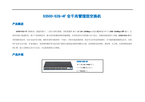
S3500-52G-4F全千兆管理型交换机产品概述S3500-52G-4F交换机是一款超多端口,二层以太网交换机。
该机型提供48个10/100/1000Mbps自适应RJ45端口+4个100M/1000Mbps SFP端口,支持所有端口线速转发。
基于千兆网络技术,最大效率的避免网络传输颈瓶,并采用业界少有的独立光口设计,突破传统的复用口局限;S3500-52G-4F采用存储转发技术,结合动态内存分配,确保有效的分配到每一个端口,同时具备流量控制,保证节点在传送和接收时,尽可能的避免数据包丢失。
该系列产品在安全可靠、多业务融合、易管理和维护等方面为用户提供全新的技术特性和解决方案,是理想的安防网络、酒店网、办公网、业务网和驻地网的汇聚、接入交换机以及中小企业、分支机构的核心交换机。
产品外观产品特点⏹多端口无阻塞高速转发S3500-52G-4F交换机提供48个10/100/1000Mbps自适应RJ45端口+4个100M/1000Mbps SFP端口,端口利用率极高。
S3500-52G-4F交换机所有端口提供二层线速交换的能力,保证所有端口无阻塞地进行报文转发。
⏹完善的安全控制策略支持端口汇聚功能,提升网络带宽的同时,通过链路备份保障网络安全;支持STP、RSTP等多种生成树协议,快速收敛,提高容错能力,保证网络的稳定运行和链路的负载均衡,合理使用网络通道,提高冗余链路利用率;支持用户端口+IP地址+MAC地址绑定,可防御内网ARP攻击和DDoS攻击;支持IP ACL、MAC ACL、Vlan ACL、支持基于三、四层的ACL功能,有效防御ARP攻击和病毒;支持半双工模式下的背压(Back-pressure)流量控制和全双工模式下的IEEE 802.3x流量控制功能,可保障在大流量数据峰值稳定交换,而不会因过度负担而导致网络瘫痪。
⏹高效的多业务融合技术提供各种类型网络接入提供完善的端到端的QoS服务质量;提供DHCP监测服务,解决了 DHCP用户的IP和端口跟踪定位问题。
FPGA可编程逻辑器件芯片XC3S100E-4FG320C中文规格书

•PMC_LSBUS_CLK is controlled by CRP PMC_LSBUS_REF_CTRL•LPD_LSBUS_CLK is controlled by CRL LPD_LSBUS_CTRLInterruptsEach controller accumulates an OR of all interrupt configured channels. If a input interrupt channel detects an event, the signal is routed to the mask register and OR'd with others to potentially assert a system interrupt signal. The system interrupt is routed to multiple destinations. The signals are listed in the IRQ System Interrupts table and several several interrupt controllers listed in the System Interrupt Controllers section. The system IRQ number for each controller:•LPD_GPIO IRQ#45•PMC_GPIO IRQ#154ErrorsThe controller detects APB address decode errors. When there is an access violation, the controller can optionally generate a SLVERR response to the master and/or generate a system error. There is no other event that can generate a system error.I/O InterfaceEach controller has multiple banks of GPIO channels routed to their local MIO multiplexers or to their PL EMIO. There are three signals from each GPIO channel: input, output, and output enable.The functionality of a channel is programmed by the GPIO Registers section.The PMC and LPD SLCR registers configure the MIO PSIO buffer. This includes input and output characteristics, and tristate control. The SLCR registers can override the signaling from the GPIO controller.The port interface signals to the PL EMIO consist of an input, output, and output enable for each channel.MIO BanksEach MIO bank:•26 channels, 26 pins•Configurable IO buffer characteristics,routing (SLCR registers)•Separate IO power rail•Aligned with a GPIO bankEMIO BanksEach EMIO bank:•32 channels, 96 signals (input, output, enable)•Aligned with a GPIO bankThe signals are listed in the GPIO I/O Signals section.Programming ModelThe GPIO controller includes a memory-mapped APB programming interface for software:•Mode and status•Output control•Input state•Interrupt configurationThe functionality of the registers is described in the GPIO Register Descriptions section.Channel Block DiagramThe functionality of a GPIO channel is illustrated in the following figure.Figure 84: GPIO Channel Block DiagramRegistersX22680-052220Input Programming ModelIn input mode, the pin voltage level is passed through a meta-stability protection circuit andtranslated to a logic level. The pin logic level is readable using the DATA_RO registers or theINT_STAT register.In the latter case, the direction control must be set to 0 for the input from the I/O pad to bepassed through to the register. There are two APB address locations allocated to the pin: A readonly location for the dedicated path and a read/write location for the registered path. The pinvalue can be read from either location in the input mode. The two paths produce different values in the output mode with inactive output enable.。
FPGA可编程逻辑器件芯片XC2S400E-4FTG256C中文规格书

Parallel Bus Bit OrderTraditionally, in SelectMAP x8 mode, configuration data is loaded one byte per CCLK, with the most-significant bit (MSB) of each byte presented to the D0 pin. Although this convention (D0 = MSB, D7 = LSB) differs from many other devices, it is consistent across all Xilinx FPGAs. The bit-swap rule also applies to Spartan-6 FPGA BPI x8 modes (see Bit Swapping, page 80).In Spartan-6 devices, the bit-swap rule is extended to x16 bus widths; the data is bit swapped within each byte.Table 5-8 and Table 5-9 show examples of a sync word inside a bitstream. These examples illustrate what is expected at the FPGA data pins when using parallel configuration modes, such as Slave SelectMAP and Master SelectMAP (BPI) modes.Delaying ConfigurationThere are two ways to delay configuration for Spartan-6 devices:•Hold the INIT_B pin Low during initialization. When INIT_B has gone High,configuration cannot be delayed by subsequently pulling INIT_B Low.•Hold the PROGRAM_B pin Low. The signals relating to initialization and delaying configuration are defined in Table 5-10.Table 5-8:Sync Word Bit Swap ExampleSync Word[31:24](1)[23:16][15:8][7:0]Bitstream Format 0xAA 0x990x550x66Bit Swapped0x550x990xAA0x66Notes:1.[31:24] changes from 0xAA to 0x55 after bit swapping.Table 5-9:Sync Word Data Sequence Example for x8 and x16 ModesCCLK Cycle 1234D[7:0] pins for x8 0x550x990xAA0x66D[15:0] pins for x160x55990xAA66Table 5-10:Signals Relating to Initialization and Delaying ConfigurationSignal Name Type Access (1)DescriptionPROGRAM_B InputExternally accessible via the PROGRAM_B pin.Global asynchronous chip reset. Can be held Low to delay configuration.INIT_BInput, Output, or Open DrainExternally accessible via the INIT_B pin.Before the Mode pins are sampled, INIT_B is an input that can be held Low to delay configuration.After the Mode pins are sampled, INIT_B is an open-drain, active-Low output that indicates whether a CRC error occurred during configurati on or a readback CRC error occurred after configuration (when enabled):0 = CRC error1 = No CRC error (needs an external pull-up)Configuration PacketsStatus Register (STAT)The Status Register indicates the value of numerous global signals. The register can be read through the SelectMAP or JTAG interfaces. Table5-35 gives the name of each bit position in the STAT register; a detailed explanation of each bit position is given in Table5-35.Table 5-35:Status Register DescriptionName Bits DescriptionSWWD_strikeout (SyncWordWatchDog)15Indicates error to configure for reasons of failure to find the sync word within the Configuration WatchDog timer(CWDT) count, invalid IDCODE, or CRC error. See theBOOTSTS register for the specific cause of failure. INITis pulled Low and SWWD_strikeout goes High.IN_PWRDN14SUSPEND status.DONE13DONEIN input from DONE pin.INIT_B12Value of INIT_B.MODE11:9Value of MODE pins (0, M1,M0).HSWAPEN8HSWAPEN status.PART_SECURED70: Decryption security not set.1: Decryption security set.DEC_ERROR6FDRI write attempted before or after decryptionoperation:0: No DEC_ERROR.1: DEC_ERROR.GHIGH_B5Status of GHIGH.GWE4Status of Global Write Enable.GTS_CFG_B3Status of Global 3-State.DCM_LOCK2DCMs and PLLs are locked.ID_ERROR1IDCODE not validated while trying to write FDRI. CRC_ERROR0CRC error.Chapter 5:Configuration DetailsConfiguration PacketsChapter 5:Configuration DetailsConfiguration Watchdog Timer RegisterThe configuration watchdog timer (CWDT) register stores the value of the number of clock cycles that the FPGA will wait before the watchdog time-out (in which SYNCWORD is not received). The default is 64k clock cycles. The minimum value is 16h'0201.HC_OPT_REG RegisterThe HC_OPT_REG register can only be reset to default by por_b.GENERAL Registers 1, 2, 3, 4, and 5GENERAL1 and GENERAL2 registers are used to store loadable multiple configuration addresses for SPI and BPI.GENERAL3 and GENERAL4 registers have a similar function as GENERAL1 andGENERAL2, except that GENERAL3 and GENERAL4 store the golden bitstream address instead of the MultiBoot address.The GENERAL5 register is a 16-bit register that allows users to store and access any extra information desired for the fail-safe scheme. These register contents are untouched during a soft reboot.These registers are set by the bitstream. BitGen can be instructed not to write to these registers using the -g next_config_register_write:Disable command. This allows the ability to store user data in the FPGA between re-configuration attempts.If the second configuration needs a previously unknown SPI vendor command, the new vendor command has already been loaded in GENERAL2 from the bitstream by this point.Table 5-39:CWDT RegisterBits Value [15:0]16h'ffffTable 5-40:HC_OPT_REG DescriptionName Bits DescriptionDefault INIT_SKIP 60: Do not skip initialization.1: Skip initialization.0RESERVED5:0Reserved.011111Table 5-41:General RegistersName Bits DescriptionGENERAL1[15:0]The lower half of the multiple boot address.GENERAL2[15:0]15:8 – SPI opcode.7:0 – Higher half of the boot address.GENERAL3[15:0]The lower half of the golden bitstream address.GENERAL4[15:0]15:8 – SPI opcode.7:0 – Higher half of the golden boot address.GENERAL5[15:0]The user-defined scratchpad register.。
FPGA可编程逻辑器件芯片XCVU9P-FLGA2104中文规格书
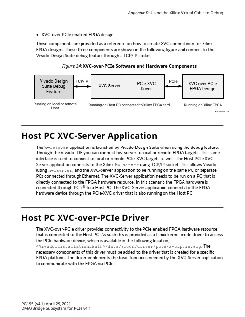
Appendix D: Using the Xilinx Virtual Cable to Debug•XVC-over-PCIe enabled FPGA designThese components are provided as a reference on how to create XVC connectivity for XilinxFPGA designs. These three components are shown in the following figure and connect to theVivado Design Suite debug feature through a TCP/IP socket.Figure 34: XVC-over-PCIe Software and Hardware ComponentsRunning on local or remoteRunning on Host PC connected to Xilinx FPGA card Running on Xilinx FPGA HostX18837-032119 Host PC XVC-Server ApplicationThe hw_server application is launched by Vivado Design Suite when using the debug feature.Through the Vivado IDE you can connect hw_server to local or remote FPGA targets. This sameinterface is used to connect to local or remote PCIe-XVC targets as well. The Host PCIe XVC-Server application connects to the Xilinx hw_server using TCP/IP socket. This allows Vivado(using hw_server) and the XVC-Server application to be running on the same PC or separatePCs connected through Ethernet. The XVC-Server application needs to be run on a PC that isdirectly connected to the FPGA hardware resource. In this scenario the FPGA hardware isconnected through PCIe® to a Host PC. The XVC-Server application connects to the FPGAhardware device through the PCIe-XVC driver that is also running on the Host PC.Host PC XVC-over-PCIe DriverThe XVC-over-PCIe driver provides connectivity to the PCIe enabled FPGA hardware resourcethat is connected to the Host PC. As such this is provided as a Linux kernel mode driver to accessthe PCIe hardware device, which is available in the following location,<Vivado_Installation_Path>/data/xicom/driver/pcie/xvc_pcie.zip. Thenecessary components of this driver must be added to the driver that is created for a specificFPGA platform. The driver implements the basic functions needed by the XVC-Server applicationto communicate with the FPGA via PCIe.PG195 (v4.1) April 29, 2021DMA/Bridge Subsystem for PCIe v4.1PCIe Ext Capability HeaderThis register is used to identify the PCIe-XVC-VSEC added to a PCIe design. The fields and values in the PCIe Ext Capability Header are defined by PCI-SIG and are used to identify the format of the extended capability and provide a pointer to the next extended capability, if applicable. When used as a PCIe-XVC-VSEC, the appropriate PCIe ID fields should be evaluated prior to interpretation. These can include PCIe Vendor ID, PCIe Device ID, PCIe Revision ID, Subsystem Vendor ID, and Subsystem ID. The provided drivers specifically check for a PCIe Vendor ID that matches Xilinx (0x10EE) before interpreting this register. The following table describes the fields within this register.Table 144: PCIe Ext Capability Header Register DescriptionBitLocation Field Description InitialValue Type15:0PCIeExtendedCapabilityIDThis field is a PCI-SIG defined ID number that indicates the natureand format of the Extended Capability. The Extended Capability IDfor a VSEC is 0x000B0x000B Read Only19:16CapabilityVersion This field is a PCI-SIG defined version number that indicates theversion of the capability structure present. Must be 0x1 for thisversion of the specification.0x1Read Only31:20NextCapabilityOffsetThis field is passed in from the user and contains the offset to thenext PCI Express Capability structure or 0x000 if no other itemsexist in the linked list of capabilities. For Extended Capabilitiesimplemented in the PCIe extended configuration space, this valuemust always be within the valid range of the PCIe ExtendedConfiguration space.0x000Read OnlyPCIe VSEC Header (PCIe-XVC-VSEC only)This register is used to identify the PCIe-XVC-VSEC when the Debug Bridge IP is in this mode. The fields are defined by PCI-SIG, but the values are specific to the Vendor ID (0x10EE for Xilinx). The PCIe Ext Capability Header register values should be qualified prior to interpreting this register.Table 145: PCIe XVC VSEC Header Register DescriptionBitLocation Field Description InitialValue Type15:0VSEC ID This field is the ID value that can be used to identify the PCIe-XVC-VSEC and is specific to the Vendor ID (0x10EE for Xilinx).0x0008Read Only19:16VSEC Rev This field is the Revision ID value that can be used to identify thePCIe-XVC-VSEC revision.0x0Read Only31:20VSECLength This field indicates the number of bytes in the entire PCIe-XVC-VSEC structure, including the PCIe Ext Capability Header and PCIeVSEC Header registers.0x020Read OnlyAppendix D: Using the Xilinx Virtual Cable to DebugPG195 (v4.1) April 29, 2021DMA/Bridge Subsystem for PCIe v4.1。
XP143 Specification-Chinese

φ0 .7 φ1 .0 φ1 .3 φ1 .8 φ2 .5 φ3 .7
φ5 .0
对应于吸嘴尺寸φ0.37~φ2.5mm 3) 吸嘴配置的限制
对应于吸嘴尺寸φ3.7~φ5.0mm
吸嘴 N o .4
吸嘴 N o .1 吸嘴 N o .10
吸嘴 N o .7
对于中型对应吸嘴φ3.7,φ5.0,安装位置 有限制。 (安装位置:吸嘴No.1,4,7,10)
5. 选 项
5.1 选项 ____________________________________________ 13
6. 机器外观
6.1 外观图 __________________________________________ 14 Spec1(前后MFU-X10E类型) ___________________________ 14
学习MSA影像处理后可以以强有力的图形匹配对所有的特殊元件方便地进行 影像处理
查找线
<创建模板例>
MSA的影像处理程序不是直接参考物理像素,而是根据虚拟影像画面,可以 在任意的位置、角度进行影像处理以达到高解析度以及高精度。
-2-
XP143-020505RS
1. 概 要
1.2.3 高生产率
1) 由于采用了独特的“ON-THE-VISION”系统和旋转工作头,实现了以周期时 间0.165秒进行贴装。此外,不像原来的多吸嘴机型那样要以同时吸取作为 前提条件,减少了因电路板的种类和元件种类的不同而产生的运转率的变 动。可以保持高的生产量。
1.2.6 与需求相对应的规格选择
在供料平台上,可以选择可以脱卸的MFU-X10E类型或者固定类型。更进一 步,可以选择Side1,Side2的双供料平台的规格,或者是仅仅Side1的单供 料平台的规格。可以从以下6种类型中选择类型。
气动阀门 4F系列 5通电磁阀 型录说明书
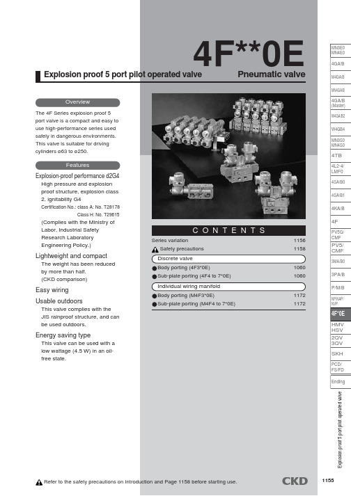
E x p l o s i o n p r o o f 5 p o r t p i l o t o p e r a t e d v a l v e1155Note 1: Effective sectional area S and sonic conductance C are converted as S 5.0 C.1156E x p l o s i o n p r o o f 5 p o r t p i l o t o p e r a t e d v a l v e11574F**0E SeriesSeries variation1158* This valve can be used in a Class 1 or Class 2 Danger Zone containing combustible gas or vapors. It cannot be used in a Class 0 Zone.Select and install the valve model following JIS C 0902, General explosion-proof rules for electrical equipment, "Ministry of Labor Industrial Safety Research Laboratory Factory Electric Facility Explosion Prevention Policy."CAUTIONWARNINGExplosive gas and explosion proof structureThe degree of explosive gas danger is classified based on the ignitability and flame-proof grade. Gases with an equivalent risk are grouped into one group, and explosion proof structurestandards are set for each group. Symbols to indicate the type, flame-proof grade, and ignitability are indicated on explosion-proof electrical devices. These symbols must be indicated in this sequence. These symbols indicate which flame-proof grade and ignitability class the electrical device has been manufactured for, and indicate which gases can be used. If d2G4 is indicated on an explosion proof solenoid valve, for example:Based on Table 1, this indicates that the valve can be used for a gas with a flame-proof grade 2 and ignitability G4. This also indicates that explosion proof properties are ensured for gases having a risk lower than this.Danger zonesAreas where explosive gases and air mix at a level high enough to cause an explosion or fire are called danger zones and are classified into Class 0, Class 1, and Class 2 zones based on the time and frequency at which the dangerous atmosphere is reached. The explosion proof structure that can be used is determined based on these classes.Class 0 zoneZone where a dangerous atmosphere is or could be continuouslygenerated, and where the concentration of explosive gas is maintained continuously or for a long time above the lower limit for explosions.Example a: Space above fluid level in container or tank of flammablefluidb: Inside combustible gas containers or tanks, etc. c: Near fluid level of flammable fluid in opened containerClass 1 zone(1) Zone where explosive gas could accumulate to a dangerousconcentration during normal operation such as during removal of a product, opening/closing of a lid, or operation of a safety valve.(2) Zone where explosive gas could frequently accumulate to a dangerous concentration during repairs, maintenance or due to a leak, etc.Class 2 zone(1) Zone where combustible or flammable fluids are handled, but where the fluids are sealed in a container or facility, and where the fluid could leak to a dangerous concentration only if the container or facility breaks or if operation is incorrect.(2) Zone where measures to prevent the accumulation of explosive gas are taken with fail-safe mechanical ventilation, but where explosive gas could accumulate to a dangerous concentration if ventilation fails.(3) Zone near or adjacent to a Class 1 zone where explosive gases could infiltrate at a dangerous concentration.Explosion proof certification no.The explosion proof certification is issued for the pilot actuator assembly.The pilot actuator assembly certification type and model are shown below.d2G4Ignitability G4Flame-proof grade 2Pressure and explosion proof structureUse in the range of box.Table 1Pneumatic componentsSafety precautionsAlways read this section before starting use.Refer to Intro 63 for valve general precautions.Explosion proof 5 port pilot operated pneumatic valve 4F**0E Series1159E x p l o s i o n p r o o f 5 p o r t p i l o t o p e r a t e d v a l v eA pilot exhaust hole is provided on the pilotactuator. Consult with CKD when using this product where problems could occur from exhaust, such as in a clean room.Do not disassemble parts of the pilot actuator other than the terminal box cap. Otherwise, explosion-proof structure performance cannot be guaranteed. Explosion-proof certification is acquired for the pilot actuator assembly. When replacing the coil,replace the pilot actuator assembly.CAUTIONWARNINGManual overrideThe manual override is provided with a lock. Turn it off when not in use. Turn the lock with a flat tip screwdriver to enable manual override.CAUTIONKeep residual leakage current within the following values:12 to 127 VAC: 4.0 mA or less 200 to 380 VAC: 2.0 mA or less12 to 48 VDC: 1.5 mA or less 80 to 125 VDC: 0.6 mA or lessCheck the leakage current to prevent malfunctions caused by currents leaking from other control devices.Note that when using a PLC, etc., which absorbs the surge voltage with the CR circuit to protect the switching element, the leakage current could flow to the CR element and adversely affect product operation.When using outdoors, use the T-type and check that rain water will not enter from lead wire outlet G1/2. The G type is for indoor use only, and must not be used outdoors.WiringWire based on JIS explosion-proof policy.Remove and wire the terminal box cap with the encloseddisassembly tool. Use the tool designated below to crimp the crimp terminal during wiring. After wiring, securely tighten the terminal box cap.Personnel must store the disassembly tool for maintenance.Select the cable for the G type from the cables below to ensure explosion-proof performance.4F3C: OFF Align characters with arrowO: ON Turn in the direction of the arrow until the lock stops.(The arrow and "O" may not necessarily be aligned.)Align • with numbers ... ON Turn in the direction of until the dial lock stops.(The • mark and may not necessarily be aligned.)111ETerminal: V2-M4 (attached)Tool: YNT-1614JST MFG CO. LTD.Terminal box capTerminal: V1.25-3 (attached)Tool: YNT-2216JST MFG CO. LTD.C K DP i l o t a c t u a t o r a s s e m b l yPilot actuator assembly(4F3 explosion proof)(4F4 to 7 explosion proof)4F**0E SeriesPrecautions1160D i s c r e t eE x p l o s i o n p r o o f 5 p o r t p i l o t o p e r a t e d v a l v e11614F**0E SeriesDiscrete valveFlow characteristicsNote 1: Effective sectional area S and sonic conductance C are converted as S 5.0 C.11624F**0E SeriesDiscrete valveHow to orderExplosion proof 5 port valve<Example of model number>4F410E-10-GP-P-X-AC100VA Model : Explosion proof 5 port pilot operated valveB Solenoid position: 2-position single solenoidC Port size : Rc3/8D Junction box : Pressure proof packing protectivetube screw-in typeE Option : Mounting bracket UF Heat proof class : HG Voltage : 100 VAC(Voltage not listed is not available. )Note 2: Order the coil as the pilot actuator assembly.Note 3: Select the cable for the G type from the cables below to ensureexplosion-proof performance.V o l t a g eAC (V) (50/60Hz)[ VDC ]12, 24, 48, 115, 120, 125, 127, 210, 230, 240, 250, 38045, 48, 80, 100, 110, 125Note 4: Consult with CKD when using for external pilot (K) vacuum pressure, cylinder port pressure, or exhaust pressure.4F3*0E Series Discrete valve: Body porting1164Internal structure and parts list Repair parts listMain parts list4F410E 4F510E 4F420E 4F520E2-position single solenoid 4F430E/4F530E 4F440E/4F540E 4F450E/4F550E3-positionAll ports closedA/B/R connection P/A/B connection2-position double solenoidNote 1 (actuator assembly)4F**0E- D P- F - GSelect from how to order on page 1162.4F4*0E/4F5*0E SeriesDiscrete valve: Sub-plate portingD i s c r e t eE x p l o s i o n p r o o f 5 p o r t p i l o t o p e r a t e d v a l v e1165Internal structure and parts listRepair parts listMain parts list4F610E 4F710E4F630E/4F730E 4F640E/4F740E 4F650E/4F750E4F620E 4F720E3-positionAll ports closed A/B/R connection P/A/B connection2-position double solenoidNote 1 (actuator assembly)4F**0E- D P- F - GSelect from how to order on page 1162.4F6*0E/4F7*0E SeriesDiscrete valve: Sub-plate porting4F3*0E Series1166D i s c r e t eE x p l o s i o n p r o o f 5 p o r t p i l o t o p e r a t e d v a l v e4F4*0E Series11674F410E2-position single solenoid4F420E2-position double solenoid4F430E3-position all ports closed4F440E3-position A/B/R connection4F450E3-position P/A/B connectionU type mounting bracket (P)4F5*0E Series11684F510E 2-position single solenoid 4F520E2-position double solenoid4F530E3-position all ports closed U type mounting bracket (P)D i s c r e t eE x p l o s i o n p r o o f 5 p o r t p i l o t o p e r a t e d v a l v e11694F6*0E SeriesDiscrete valve: Sub-plate porting4F610E2-position single solenoid4F620E2-position double solenoid4F630E3-position all ports closed4F640E3-position A/B/R connection4F650E3-position P/A/B connectionU type mounting bracket (P)11704F710E 2-position single solenoid 4F720E2-position double solenoid4F730E3-position all ports closed 4F740E3-position A/B/R connection4F750EU type mounting bracket (P)4F7*0E SeriesD i s c r e t eE x p l o s i o n p r o o f 5 p o r t p i l o t o p e r a t e d v a l v e11714F**0E SeriesDiscrete valveT type (standard)Conduit screw connection methodT type (standard)Conduit screw connection method G type (option)The manual override is provided with a lock. Turn it off when not in use. Turn the lock with a flat tip screwdriver to enable manual override.4F3C: OFF Align characters with arrowO: ON Turn in the direction of the arrow until the lock stops.(The arrow and "O" may not necessarily be aligned.) 4F4/5/6/7... OFF Align • with numbers ... ON Turn in the direction of until the dial lock stops.(The • mark and may not necessarily be aligned)111<Safety precautions>DimensionsAfter piping outdoors, check that water will not enter even if left outside without electrical piping.(Water could enter into the wiring box.)Select the cable for the G type from the cables below to ensure*The external pilot port position is common for 4F4 to 4F7.4F4 to 4F7External pilot port: (K)11721173I n d i v i d u a l w i r i n g m a n i f o l d E x p l o s i o n p r o o f 5 p o r t p i l o t o p e r a t e d v a l v eM4F**0E SeriesIndividual wiring manifoldFlow characteristicsNote 1: Effective sectional area S and sonic conductance C are converted as S 5.0 x C.M4F**0E Series Individual wiring manifoldHow to orderDiscrete solenoid valve of manifold (4F4 to 7) Discrete solenoid valve of manifold (4F3)9P11741175I n d i v i d u a l w i r i n g m a n i f o l d E x p l o s i o n p r o o f 5 p o r t p i l o t o p e r a t e d v a l v eM4F**0E SeriesIndividual wiring manifoldHow to order masking plate kit2S1S2S3S4S5MP 21110Indicate the quantity.How to Order Mixed Manifold Models(1) Indicate the quantity for each function (solenoid position) at the end of the model.Functions and symbols are indicated below.(2) Indicate the function (solenoid position) and layout position in the remarks field.Example: 2-position single solenoid —› S1Example: S1 = 1, 6 (1, 6th station is 2-position single solenoid.)2-position single solenoid (S1): 2 piece (1st and 6th station)2-position double solenoid (S2): 2 piece (2nd and 5th station)3-position all ports closed (S3): 1 piece (3rd station)3-position A/B/R connection (S4): 1 piece (7th station)3-position P/A/B connection (S5): 1 piece (4th station)M4F380E-08-TP-N-7-CU-AC100V<Example of model number>For 7 stationsSolenoid position = , th station (facing the piping port, the left side is the 1st station.)LayoutSymbolS1 = 1, 6 S2 = 2, 5 S3 = 3S4 = 7 S5 = 42S1S2S3S4S5MP21110How to order mix manifold0E 2S1S2S3S4S5MP21110S1 = 1, 6 S2 = 2, 5S3 = 3 S4 = 7S5 = 4* Refer to previous page for how to order other parts.1176CL (common exhaust type)IL (individual exhaust type)L bracket attachedM4F310E- -TP-This is Z section when individual exhaustStation numberNo.2No.1No.3No.nA View A Supply port0810M4F3*0E Series1177I n d i v i d u a l w i r i n g m a n i f o l d E x p l o s i o n p r o o f 5 p o r t p i l o t o p e r a t e d v a l v e0810CU (common exhaust type)IU (individual exhaust type)M4F3*0E- -TP-This is Z section when individual exhaustStation number · · · · ·No.1No.2No.nAView ASupply portU bracket attachedM4F3*0E Series1178M4F4*0E/M4F5*0E SeriesM4F5*0E-10-TP-*-CM4F4*0E-08-TP-*-C* Enlarged view of installation hole.1179I n d i v i d u a l w i r i n g m a n i f o l d E x p l o s i o n p r o o f 5 p o r t p i l o t o p e r a t e d v a l v eM4F6*0E/M4F7*0E SeriesIndividual wiring manifold: Sub-plate portingM4F6*0E-D15-TP-*-CM4F7*0E-E20-TP-*-C。
SG2023中文资料
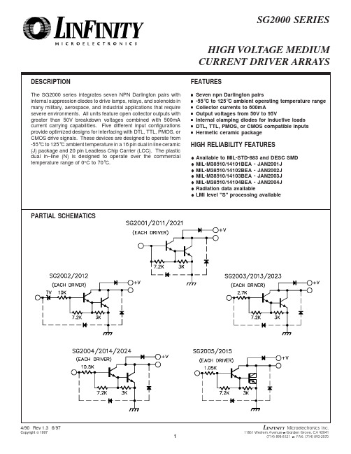
HIGH VOLTAGE MEDIUM CURRENT DRIVER ARRAYSABSOLUTE MAXIMUM RATINGS (Note 1)Peak Collector Current, I C(SG2000, 2020) ......................................................(SG2010) ................................................................Operating Junction TemperatureHermetic (J, L Packages) .........................................Plastic (N, Packages) ...............................................Storage Temperature Range ..........................Lead Temperature (Soldering 10 sec.) .........................Output Voltage, V CE(SG2000, 2010 series) ................................................(SG2020 series) ..........................................................Input Voltage, V IN(SG2002,3,4) ...............................................................Continuous Input Current, I IN ........................................50V 95V 30V 25mA500mA 600mA 150°C 150°C -65°C to 150°C 300°CNote 1. Values beyond which damage may occur.J Package:Thermal Resistance-Junction to Case , θJC .................. 30°C/W Thermal Resistance-Junction to Ambient , θJA ...............80°C/W N Package:Thermal Resistance-Junction to Case , θJC .................. 40°C/W Thermal Resistance-Junction to Ambient , θJA .............. 65°C/W L Package:Thermal Resistance-Junction to Case , θJC .................. 35°C/W Thermal Resistance-Junction to Ambient , θJA ............ 120°C/WTHERMAL DATANote A.Junction Temperature Calculation: T J = T A + (P D x θJA ).Note B.The above numbers for θJC are maximums for the limiting thermalresistance of the package in a standard mounting configuration.The θJA numbers are meant to be guidelines for the thermal performance of the device/pc-board system. All of the above assume no ambient airflow.Output Voltage, V CESG2000, SG2010 series ..............................................SG2020 series .............................................................50V 95VPeak Collector Current, I CSG2000, SG2020 series ...........................................SG2010 series ........................................................Operating Ambient Temperature RangeSG2000 Series - Hermetic ..........................SG2000 Series - Plastic ..................................50mA 500mA -55°C to 125°C 0°C to 70°CRECOMMENDED OPERATING CONDITIONS (Note 2)Note 2. Range over which the device is functional.SELECTION GUIDEDevice V CE Max I C Max Logic InputsSG200150V 500mA General Purpose PMOS, CMOS SG200250V 500mA 14V-25V PMOS SG200350V 500mA 5V TTL, CMOSSG200450V 500mA 6V-15V CMOS, PMOS SG201150V 600mA General Purpose PMOS, CMOS SG201250V600mA14V-25V PMOSDevice V CE Max I C Max Logic InputsSG201350V 600mA 5V TTL, CMOSSG201450V 600mA 6V-15V CMOS, PMOS SG201550V 600mA High Output TTL SG202195V 500mA General Purpose PMOS, CMOS SG202395V 500mA 5V TTL, CMOSSG202495V500mA6V-15V CMOS, PMOSCHARACTERISTIC CURVESFIGURE 4.INPUT CHARACTERISTICS - SG2002FIGURE 5.INPUT CHARACTERISTICS - SG2003FIGURE 6.INPUT CHARACTERISTICS - SG2004FIGURE 7.PEAK COLLECTOR CURRENT VS. DUTY CYCLEFIGURE 1.OUTPUT CHARACTERISTICS FIGURE 2.OUTPUT CURRENT VS. INPUT VOLTAGE FIGURE 3.OUTPUT CURRENT VS. INPUT CURRENTNote 1. Contact factory for JAN and DESC product availability.2. All parts are viewed from the top.3. See selection guide for specific device types.CONNECTION DIAGRAMS & ORDERING INFORMATION (See Notes Below)AmbientTemperature Range Part No. (Note 3)PackageConnection Diagram16-PIN CERAMIC DIP J - PACKAGESG2XXXJ/883B -55°C to 125°C SG2023J/DESC -55°C to 125°C JAN2001J -55°C to 125°C JAN2002J -55°C to 125°C JAN2003J -55°C to 125°C JAN2004J -55°C to 125°C SG2XXXJ-55°C to 125°C17654328109111213141615SG2003N 0°C to 70°C SG2023N 0°C to 70°C16-PIN PLASTIC DIP N - PACKAGE20-PIN CERAMICLEADLESS CHIP CARRIER L- PACKAGESG2XXXL/883B -55°C to 125°C SG2XXXL -55°C to 125°C1849319201214151716876513121110。
FPGA可编程逻辑器件芯片XC2S150-4FG456C中文规格书
Chapter1 Introduction to the RocketIO GTX TransceiverOverviewThe RocketIO™ GTX transceiver is a power-efficient transceiver for Virtex®-5 FPGAs. TheGTX transceiver is highly configurable and tightly integrated with the programmable logicresources of the FPGA. It provides the following features to support a wide variety ofapplications:•Current Mode Logic (CML) serial drivers/buffers with configurable termination,voltage swing, and coupling.•Programmable TX pre-emphasis, RX equalization, and linear and decision feedbackequalization (DFE) for optimized signal integrity.•Line rates from 750Mb/s to 6.5Gb/s, with optional 5x digital oversampling requiredfor rates between 150Mb/s and 750Mb/s. The nominal operation range of the sharedPMA PLL is from 1.5GHz to 3.25GHz. These are nominal values, see DS202: Virtex-5FPGA Data Sheet for specifications.•Optional built-in PCS features, such as 8B/10B encoding, comma alignment, channelbonding, and clock correction.•Fixed latency modes for minimized, deterministic datapath latency.•Beacon signaling for PCI Express® designs and Out-of-Band signaling includingCOM signal support for SATA designs.•RX/TX Gearbox provides header insertion and extraction support for 64B/66B and64B/67B (Interlaken) protocols.•Receiver eye scan:♦Vertical eye scan in the voltage domain for testing purposes♦Horizontal eye scan in the time domain for testing purposesThe first-time user is recommended to read High-Speed Serial I/O Made Simple[Ref1], whichdiscusses high-speed serial transceiver technology and its applications.Table1-1 lists some of the standard protocols designers can implement using the GTXtransceiver. The Xilinx® CORE Generator™ tool includes a Wizard to automaticallyconfigure GTX transceivers to support one of these protocols or perform customconfiguration (see Chapter2, “RocketIO GTX Transceiver Wizard”).The GTX_DUAL tile offers a data rate range and features that allow physical layer supportfor various protocols as illustrated in Table1-1.Preface:About This GuideAdditional Documentation•Virtex-5 Family OverviewThe features and product selection of the Virtex-5 family are outlined in this overview.•Virtex-5 FPGA Data Sheet: DC and Switching CharacteristicsThis data sheet contains the DC and Switching Characteristic specifications for theVirtex-5 family.•Virtex-5 FPGA User GuideThis user guide includes chapters on:♦Clocking Resources♦Clock Management Technology (CMT)♦Phase-Locked Loops (PLLs)♦Block RAM♦Configurable Logic Blocks (CLBs)♦SelectIO™ Resources♦SelectIO Logic Resources♦Advanced SelectIO Logic Resources•Virtex-5 FPGA RocketIO GTP Transceiver User GuideThis guide describes the RocketIO™ GTP transceivers available in the Virtex-5 LXTand SXT platforms.•Virtex-5 FPGA Embedded Processor Block for PowerPC® 440 DesignsThis reference guide is a description of the embedded processor block available in theVirtex-5 FXT platform.•Virtex-5 FPGA Tri-Mode Ethernet Media Access ControllerThis guide describes the dedicated Tri-Mode Ethernet Media Access Controlleravailable in the Virtex-5 LXT, SXT, FXT, and TXT platforms.•Virtex-5 FPGA Integrated Endpoint Block User Guide for PCI Express DesignsThis guide describes the integrated Endpoint blocks in the Virtex-5 LXT, SXT, FXT, andTXT platforms used for PCI Express® designs.•XtremeDSP Design ConsiderationsThis guide describes the XtremeDSP™ slice and includes reference designs for usingthe DSP48E slice.•Virtex-5 FPGA Configuration GuideThis all-encompassing configuration guide includes chapters on configurationinterfaces (serial and SelectMAP), bitstream encryption, Boundary-Scan and JTAGconfiguration, reconfiguration techniques, and readback through the SelectMAP andJTAG interfaces.•Virtex-5 FPGA System Monitor User GuideThe System Monitor functionality available in all the Virtex-5 devices is outlined inthis guide.Additional Support Resources•Virtex-5 FPGA Packaging and Pinout SpecificationsThis specification includes the tables for device/package combinations and maximumI/Os, pin definitions, pinout tables, pinout diagrams, mechanical drawings, andthermal specifications.•Virtex-5 FPGA PCB Designer’s GuideThis guide provides information on PCB design for Virtex-5 devices, with a focus onstrategies for making design decisions at the PCB and interface level.The following documents provide supplemental material useful to this user guide:1.Athavale, Abhijit and Carl Christensen. High-Speed Serial I/O Made Simple.2.UG200, Embedded Processor Block in Virtex-5 FPGAs Reference Guide.3.UG626, Synthesis and Simulation Design Guide.4.Granberg, Tom. Handbook of Digital Techniques for High-Speed Design. Prentice-Hall. ISBN-10:1-13-142291-X. ISBN-13: 978-0131422919.5.Grover, Frederick W., Ph.D. 1946. Inductance Calculations: Working Formulas and Tables. NewYork: D. Van Nostrand Company, Inc.6.Johnson, Howard, Martin Graham. High-Speed Signal Propagation: Advanced Black Magic.Prentice-Hall. ISBN-10: 0-13-084408-X. ISBN-13: 978-0130844088.7.Montrose, Mark I. 1999. EMC and the Printed Circuit Board. The Institute of Electrical andElectronics Engineers, Inc. ISBN 0-7803-4703-X.8.Smith, Larry D. November 1984. Decoupling Capacitor Calculations for CMOS Circuits.Proceedings EPEP Conference.9.Williams, Ross N. The Painless Guide to CRC Error Detection Algorithms.10.Schlichthaerle, Dietrich. Digital Filters: Basics and Design. Springer. ISBN-10 3-540-66841-1.11.DS083, Virtex-II Pro and Virtex-II Pro X Platform FPGAs Complete Data Sheet.12.UG024, RocketIO Transceiver User Guide.13.UG076, Virtex-4 RocketIO Multi-Gigabit Transceiver User Guide.14.XAPP209, IEEE 802.3 Cyclic Redundancy Check.15.XAPP562, Configurable LocalLink CRC Reference Design.16.UG196, Virtex-5 FPGA RocketIO GTP Transceiver User Guide.17.UG204, LogiCORE IP Virtex-5 FPGA RocketIO GTX Transceiver Wizard v1.6 Getting StartedGuide.Additional Support ResourcesPreface:About This GuideSection 1: FPGA Level Design。
天网防火墙CCS-FW-4545TC参数表
天网防火墙CCS-FW-4545TC参数表背景1来自与公网互联的安全威胁深圳公安局公交分局的网络将与Internet连接。
基于Internet公网的开放性、国际性与自由性,内部网络将面临更加严重的安全威胁。
因为,每天黑客都在试图闯入Internet节点,假如我们的网络不保持警惕,可能连黑客怎么闯入的都不知道,甚至会成为黑客入侵其他网络的跳板。
由于内部网络中其办公系统及各人主机上都有涉密信息。
假如内部网络的一台机器安全受损(被攻击或者被病毒感染),就会同时影响在同一网络上的许多其他系统。
透过网络传播,还会影响到与本系统网络有连接的外单位网络。
如果系统内部局域网络与系统外部网络间没有采取一定的安全防护措施,内部网络容易造到来自外网一些不怀好意的入侵者的攻击。
如: 入侵者通过漏洞扫描、Sniffer嗅探等工具来探测扫描网络及操作系统存在的安全漏洞,如网络IP地址、应用操作系统类型、开放哪些服务端口号、系统保存用户名和口令等安全信息的关键文件等,并通过相应攻击程序对内网进行攻击;●入侵者通过网络监听等先进手段获得内部网用户的用户名、口令等信息,进而假冒内部合法身份进行非法登录,窃取内部网重要信息;●恶意攻击:入侵者通过发送大量PING包对内部网重要服务器进行攻击,使得服务器超负荷工作以至拒绝服务甚至系统瘫痪;●发送大量包含恶意代码或病毒程序的邮件。
2内部局域网的安全威胁据调查在已有的网络安全攻击事件中约70%是来自内部网络的侵犯。
来自机构内部局域网的威胁包括:●误用和滥用关键、敏感数据和计算资源。
无论是有不满情绪的员工的故意破坏,还是没有访问关键系统权限的员工因误操作而进入关键系统,由此而造成的数据泄露、偷窃、损坏或删除将给企业带来很大的负面影响。
●因不当使用Internet接入而降低生产率。
不当使用Internet资源不但会浪费工人的时间,还能增加计算机网络的负担,降低了人员与网络的工作效率。
●如果工作人员发送、接收和查看攻击性材料,可能会形成敌意的工作环境,从而增大内耗。
sgc440执行标准

sgc440执行标准SGC440执行标准。
SGC440是一种用于热镀锌板的材料,其执行标准对于生产和质量控制至关重要。
本文将对SGC440执行标准进行详细介绍,以便于相关人员了解和遵循。
1. 材料成分要求。
SGC440的执行标准对其成分有严格的要求。
其中包括各种元素的含量限制,如碳(C)、硅(Si)、锰(Mn)、磷(P)、硫(S)等。
这些成分的控制对于保证热镀锌板的性能和质量至关重要,生产过程中需要严格按照标准进行控制。
2. 机械性能要求。
除了成分要求外,SGC440的执行标准还对其机械性能有着明确的规定。
这包括抗拉强度、屈服强度、延伸率等指标的要求。
这些机械性能的要求直接关系到热镀锌板在使用过程中的性能表现,因此在生产过程中需要严格控制各项工艺参数,以保证产品达到标准要求。
3. 表面质量要求。
热镀锌板作为一种外表面涂层钢板,其表面质量对于最终产品的外观和耐候性有着重要影响。
SGC440的执行标准对其表面质量有着严格的要求,包括镀层附着力、表面平整度、表面处理等方面。
这些要求需要在生产过程中加强表面质量的控制,确保产品符合标准要求。
4. 尺寸和允许偏差。
除了上述方面的要求外,SGC440的执行标准还对其尺寸和允许偏差有着详细规定。
这包括板厚、宽度、长度等方面的要求,同时也对于尺寸偏差有着严格的限制。
生产过程中需要加强对产品尺寸的控制,以确保产品符合标准要求。
5. 包装和标识要求。
最后,SGC440的执行标准还对其包装和标识有着明确规定。
这包括包装方式、包装标识、产品标识等方面的要求。
在产品出厂前,需要对其包装和标识进行严格检查,确保符合标准要求。
总结。
SGC440执行标准对于热镀锌板的生产和质量控制有着严格的要求,涵盖了材料成分、机械性能、表面质量、尺寸偏差、包装标识等方面。
生产企业需要加强对这些方面的控制,确保产品符合标准要求,为用户提供优质的热镀锌板产品。
同时,相关部门也需要加强对产品的监督检查,确保市场上的产品符合执行标准,保障用户权益和产品质量。
FPGA可编程逻辑器件芯片XCVU13P-2FHGB2104CE中文规格书

Chapter1 Packaging OverviewIntroduction to the UltraScale ArchitectureThe Xilinx® UltraScale™ architecture is the first ASIC-class architecture to enablemulti-hundred gigabit-per-second levels of system performance with smart processing,while efficiently routing and processing data on-chip. UltraScale architecture-based devices address a vast spectrum of high-bandwidth, high-utilization system requirements by using industry-leading technical innovations, including next-generation routing, ASIC-likeclocking, 3D-on-3D ICs, multiprocessor SoC (MPSoC) technologies, and new powerreduction features. The devices share many building blocks, providing scalability acrossprocess nodes and product families to leverage system-level investment across platforms.Virtex® UltraScale+™ devices provide the highest performance and integration capabilities in a FinFET node, including both the highest serial I/O and signal processing bandwidth, as well as the highest on-chip memory density. As the industry's most capable FPGA family, the Virtex UltraScale+ devices are ideal for applications including 1+Tb/s networking and data center and fully integrated radar/early-warning systems.Virtex UltraScale devices provide the greatest performance and integration at 20nm,including serial I/O bandwidth and logic capacity. As the industry's only high-end FPGA at the 20nm process node, this family is ideal for applications including 400G networking, large scale ASIC prototyping, and emulation.Kintex® UltraScale+ devices provide the best price/performance/watt balance in a FinFET node, delivering the most cost-effective solution for high-end capabilities, includingtransceiver and memory interface line rates as well as 100G connectivity cores. Our newest mid-range family is ideal for both packet processing and DSP-intensive functions and is well suited for applications including wireless MIMO technology, Nx100G networking, and data center.Kintex UltraScale devices provide the best price/performance/watt at 20nm and include the highest signal processing bandwidth in a mid-range device, next-generationtransceivers, and low-cost packaging for an optimum blend of capability andcost-effectiveness. The family is ideal for packet processing in 100G networking and data centers applications as well as DSP-intensive processing needed in next-generation medical imaging, 8k4k video, and heterogeneous wireless infrastructure.Gigabit Transceiver Channels by Device/PackageTable 1-2 lists the quantity of gigabit transceiver channels for the UltraScale andUltraScale+ devices. In all devices, a gigabit transceiver channel is one set of MGTRXP, MGTRXN, MGTTXP, and MGTTXN pins. For transceiver data rate limitations on specific device/package combinations, see the specific UltraScale and UltraScale+ device data sheets [Ref 4].FSVA3824SSI, flip-chip, fine-pitch, lidless with stiffener ring BGA 1.065x 65FSVB3824SSI, flip-chip, fine-pitch, lidless with stiffener ringBGA1.065x 65Notes:1.FFV, FLV, and FLG packages are footprint compatible when the package code letter designator and pin count are identical.See UltraScale Architecture and Product Overview (DS890) [Ref 1] for specific letter codes and ordering code information.2.These 52.5x 52.5 packages have the same PCB ball footprint as the 47.5x 47.5 packages and are footprint compatible.Table 1-1:Package Specifications (Cont’d)Packages (1)DescriptionPackage SpecificationsPackage Type Pitch (mm)Size (mm)Table 1-2:Serial Transceiver Channels (GTH/GTY) by Device/PackageDevicePackageGTH ChannelsGTY ChannelsKintex UltraScale DevicesXCKU035FBVA676160XCKU040160XCKU035SFVA78480XCKU04080XCKU035FBVA900160XCKU040160XCKU025FFVA1156120XCKU035160XCKU040200XCKU060280XCKU095208XCKU060FFVA1517320XCKU085FLVA1517480XCKU115480XCKU095FFVC15172020XCKU115FLVD1517640XCKU095FFVB17603216XQVU3P FFRC1517040XQVU7P FLRA2104052XQVU7P FLRB2104076XQVU11PFLRC210496DevicePackage GTH Channels GTY Channels GTM ChannelsVirtex UltraScale+ DevicesXCVU27P FIGD210401630XCVU29P 01630XCVU27P FSGA257703248XCVU29P3248DevicePackage GTH ChannelsGTY Channels。
Globe Food Equipment Company GFP 700 750 裂切机部件目录说明

F O O D P R O C E S S O R SMODE L : G FP 700/750IMP OR TANT!TO E XP E DITE S HIP ME NT OF P AR TS , ALWAY S S P E C IF Y MODE L,R E V,P AR T NUMB E R , AND S E R IAL NUMB E R OF P R OC E S S OR.GLOBE FOOD EQUIPMENT COMPANY2268 N. Moraine Drive Dayton, Ohio 45439Parts DepartmentToll Free 1-800-745-6238 Fax (937) 290-0585E-Mail:**************************Website: Model G F P 7001-1-2002Parts Catalogue1.A.2.3.4.NOT SHOWN 5.6.7.8.9.10.11.12.13.14.15.16.NOT SHOWNUPPER HOUSING ASSEMBL Y(INCLUDES SHAFT, BEARINGS, & HARDWARE)UPPER HOUSINGBASE CASTINGBOTTOM ENCLOSURERUBBER FOOT (4 REQUIRED)FOOT SCREWS (4 REQUIRED)HINGE PINSTRAIN RELIEFREED SWITCH(GLIDE ROD) WHITEREED SWITCH (ON/OFF) BLACKPIVOT LA TCH SCREWMOUNTING PLA TECLIP RINGCLIP RINGBALL BEARINGUPPER BEARING SEALDRIVE SHAFTLABELBOTTOM CLOSURE SCREWHOUSING MOUNTING SCREWHOUSING MOUNTING LOCKWASHERF3512180F3512171F3512178F3512177F3521104F8023102F3512110F7063023F7084018F7084015F3511106F3511113F8151354F8152264F8232473F7351015F3512162871-3F8032182F8013341F81410562123444456789101112131415161. A.2.3.4.6.7.8.9.10.11.12.13.14.15.16.17.18.19.20.21.22.23.24.25.26.27.HINGE LID ASSEMBL Y HINGE LIDALUMINUM FOOD PUSHER WARNING LABEL GLIDE ROD SETAXLE AND 2 KNURL NUTS AXLE KNURL NUT (2 REQUIRED )ON/OFF LABELLA TCH ASSEMBL Y (INCLUDES F 3511119)PIVOT LA TCH PIN LA TCH ROLLERHEAD LA TCH BUSHINGS (3 REQ)END PIECEPINION SHAFT PINION BUSHINGLIP SEAL PINION SHAFT CLIP RING SEAL RING LIP SEALFLANGE BUSHING INLETSLIDE BEARING O-RING O-RINGGLIDE ROD PIN CENTERING RING INSERT RINGF 3112166F 3512167F 3512127F0000003F 3512184F 3512183F 3521602F0000002F 3511150F 3511118F 3511119F 8213067F 3511123F 3512133F 8211485F 8262464F 7349012F 3512134F 8263884F 8214087F 3512142F 3522105F 3512145F 8253354F 8182228F 3512144F 3512143(INCLUDES ALL PARTS )31242067121415161718192221222327248261093131125701.A. 2. 3. 4. 6. 7. 8. 9.10.11.12.13.14.15.HINGE LID ASSEMBL Y(INCLUDES ALL PARTS)HINGE LIDALUMINUM FOOD PUSHERWARNING LABELGLIDE ROD SETAXLE & 2 KNURL NUTSAXLE KNURL NUTON/OFF LABELLA TCH ASSEMBL Y (INCLUDES F3511119)PIVOT LA TCH PINEND PIECEGLIDE ROD PINFLANGE BUSHINGHEAD LA TCH BUSHINGS(3 REQ)LA TCH ROLLERF3112165F3512166F3512127F0000003F3512184F3512183F3521602F0000002F3511150F3511118F3511123F8182228F8214087F8213067F3511119412346710159131411121.2.3.4.5.6.NOT SHOWNCORDMOTOR AND GEARBOXMOTOR AND GEARBOX(GFP "R-SERIES)RELA Y/POWER SUPPL YOVERLOAD HEA TERSPOWER RELA YCAP ACITORMOUNTING PLA TEMOTOR MOUNTING STUD(4 REQ)MOTOR MOUNTING WASHER(4 REQ)MOTOR MOUNTING NUT(4 REQ)132-3F7335019F7335038F7079003F7072047F7072038F7051009F3512169F8093141F8141056F810106112345765GFP 700-750CAPACITOR REED SWITCHS12345N LC 1K-1K-2ON/OFFPUSHER 135246115V A-1A-2CONTACTOR WITH OVERLOAD POWER SUPPLY/RELAY ASSY F7079003CORD 132-3MOTOR F 7335019F 7051009F 7072038F 7072047F7084015F7084018。
SGC资料
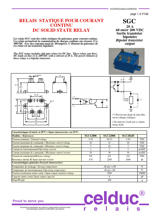
SGC12006
3-16 16 3 1 30 0,8 470
SGC22006
10-32 32 10 1 30 0,8 2200 - 40 à/to +150 -40 à/to +80 2500 8 100
SGC20420
3-30 30 3 1 30 0,8 1000 VDC VDC VDC mADC mADC VDC Ω °C °C VRMS pF g
22 20
/W °C 0,5
Caractéristiques thermiques / thermal curves :
18 16 14 12 Courant commuté (A) / Switched current (A) 10 8 6 4 2 0 0
1° C/ W
2°C /W
10 20 30 40 50 60 70 80 90 Température ambiante (°C) / Ambient temperature (°C)
SGC12006
2 à/to 60 60 20 30 2 1 5 200 800 0 à/to 500 200
SGC22006
2 à/to 60 60 20 30 2 1 5 200 800 0 à/to 500 200 Nous consulter
SGC20420
2 à/to 200 200 20 30 2 1 5 200 800 0 à/to 500 200 Consult us VDC VDC VPEAK A APEAK VDC mA mA µs µs Hz V/µs
Proud to serve you
All technical caracteristics are subject to change without previous notice. Caractéristiques sujettes à modifications sans préavis.
FPGA可编程逻辑器件芯片XC3S100E-4FG320GI中文规格书

System SignalsClocksEach controller receives its own reference clock and the APB programming interface clock.The clock programming is described in the Configure Clocks section.ResetsThe controller has one reset state that is entered when the device is locally reset by the SW_Reset register, or by a software reset that includes the LPD, or a POR reset.The reset control is described in the Reset Controller :System InterruptEach I2C controller generates a system interrupt based events and programming of the I2C interrupt mask register. The IRQ number are shown in Block Diagram . These IRQ numbers are included in the device-level IRQ System Interrupts table. The I2C interrupt programming is described in the Interrupts section.I/O InterfaceThe options for routing the I2C two wire I/O interface include the LPD MIO pins, the PMC MIO pins, and the PL EMIO. The options are shown in I2C I/O Interface section and in the device-level MIO-at-a-Glance table.Programming ModelThe following sections describe how to program and use the I2C controller.Programming InterfaceThe I2C controllers includes a simple memory-mapped APB programming interface for software:•Control and status registers•Transmit data register port•Receive data register portSection XII: I/O Peripheral ControllersChapter 69: I2C ControllerAM011 (v1.1) November 30, 2020Versal ACAP TRMReset ControllerThe following register bits can be used to reset a I2C controller.•LPD I2C0 reset is controlled by the CRL RST_LPD_I2C0 register•LPD I2C1 reset is controlled by the CRL RST_LPD_I2C1 register•PMC I2C reset is controlled by the PMC RST_I2C registerThe [RESET] bits must be toggled by software:•0: Run mode•1: Reset stateConfigure I/O SignalsThe SCL and SDA signals can be routed to one of many sets of MIO pins or to the PL EMIO port signal interface by default.The signal for each MIO pin is routed using SLCR registers:•MIO_Pin_0 through MIO_PIN_51•MIO_PIN_0 through MIO_PIN_25The IOP_SLCR.LPD_MIO_SEL [CANx] register bit selects between the PMC and LPD MIO pin multiplexers.If a MIO PIN register does not map an I2C I/O pin, then the signal is available as an EMIO port interface signal. The SLCR registers also configure the MIO pin buffer input and outputcharacteristics. The I2C I/O signals are listed in I2C I/O Interface .Configure ClocksClocks are generated by the PMC and LPD clock controllers. The clock generators are described in System Perspective .The I2C controller receives two clocks.APB Programming Interface ClockThe APB programming interface is driven by the low-speed interconnect clock. Each register includes the three fields [SRCSEL], [DIVISOR], and [CLKACT].Control registers:•PMC_I2C: PMC_LSBUS_CLKSection XII: I/O Peripheral ControllersChapter 69: I2C ControllerAM011 (v1.1) November 30, 2020Versal ACAP TRM•LPD_I2C{0, 1}: LPD_LSBUS_CLKReference ClockThe reference clock is used for the controller logic, registers, and memories. It is also an input to the baud rate generator. Each I2C controller has its own reference clock that comes from the PMC or LPD clock generator. Each register includes the three fields [SRCSEL], [DIVISOR], and[CLKACT].Clock control registers:•PMC_I2C_REF_CLK controlled by the CRP I2C_REF_CTRL register•LPD_I2C0_REF_CLK controlled by the CRL I2C0_REF_CTRL register•LPD_I2C1_REF_CLK controlled by the CRL I2C1_REF_CTRL registerInterruptsThe Interrupt Status register (LPD_I2C.ISR) bits are sticky and masked by the Interrupt Maskregister, LPD_I2C.IMR. Non-masked interrupts are OR'd together to generate a system interrupt.•LPD_I2C0 = IRQ#46•LPD_I2C1 = IRQ#47•PMC_I2C = IRQ#155Transfer CompleteThe COMP interrupt bit functionality depends on the interface mode and the interface activity.Master ModeIn master write, this bit is always set when all the supplied data is successfully written to theslave and the transfer is about to be terminated with a stop sequence. If the HOLD bit is set, the COMP bit is also set as soon as the data is successfully written to the slave, but the transfer is not terminated at this point. This allows for combined transfers to be performed even when FIFO is implemented. If the host clears the HOLD bit instead of continuing the transfer, the COMP bit is set again during the stop sequence generation.In master read, this bit is set when all the requested data has been successfully read from a slave and the transfer is to be terminated with a stop sequence.If FIFO is implemented and hold bit is set, COMP bit is also set as soon as all data is successfully received from the slave, but transfer is not terminated at this point. This allows for combined transfers to be performed even when FIFO is implemented. If the host clears the HOLD bit instead of continuing the transfer, COMP bit is set again during the stop sequence generation.Slave ModeSection XII: I/O Peripheral ControllersChapter 69: I2C ControllerAM011 (v1.1) November 30, 2020Versal ACAP TRM。
FPGA可编程逻辑器件芯片XC3S200A-4FTG256I中文规格书
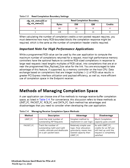
When calculating the number of completion credits a non-posted request requires, you must determine how many RCB-bounded blocks the completion response might be required, which is the same as the number of completion header credits required. Important Note For High Performance ApplicationsWhile a programmed RCB value can be used by the user application to compute the maximum number of completions returned for a request, most high performance memory controllers have the optional feature to combine RCB-sized completions in response to large read requests (read lengths multiples of RCB value), into completions that are at or near the programmed Max_Payload_Size value for the link. You are encouraged to take advantage of this feature, if supported, by a memory controller on the host CPU. Data exchange based on completions that are integer multiples (>1) of RCB value results in greater PCI Express interface utilization and payload efficiency, as well as, more efficient use of completion space in the Endpoint receiver.Methods of Managing Completion SpaceA user application can choose one of five methods to manage receive-buffer completion space, as listed in Table C-4. For convenience, this discussion refers to these methods as LIMIT_FC, PACKET_FC, RCB_FC, and DATA_FC. Each method has advantages and disadvantages that you need to consider when developing the user application.Table C-3:Read Completion Boundary Settings cfg_rcb_status[0] or cfg_rcb_status[1]Read Completion BoundaryBytesDW QW Credits 0641684112832168Table C-4:Managing Receive Completion Space MethodsMethod DescriptionAdvantage Disadvantage LIMIT_FC Limit the total number of outstanding NP RequestsSimplest method to implement in user logic Much Completion capacity goes unused PACKET_FC Track the number of outstanding CplH and CplD credits; allocate and deallocate on a per-packet basis Relatively simple user logic; finer allocation granularity means less wasted capacity than LIMIT_FC As with LIMIT_FC, credits for an NP are still tied up until the request is completely satisfiedLIMIT_FC MethodThe LIMIT_FC method is the simplest to implement. The user application assesses the maximum number of outstanding Non-Posted Requests allowed at one time, MAX_NP. To calculate this value, perform these steps:1.Determine the number of CplH credits required by a Max_Request_Size packet:Max_Header_Count = ceiling(Max_Request_Size / RCB)2.Determine the greatest number of maximum-sized completions supported by the CplD credit pool:Max_Packet_Count_CplD = floor(CplD / Max_Request_Size)3.Determine the greatest number of maximum-sized completions supported by the CplH credit pool:Max_Packet_Count_CplH = floor(CplH / Max_Header_Count)e the smaller of the two quantities from steps 2 and 3 to obtain the maximum number of outstanding Non-Posted requests:MAX_NP = min(Max_Packet_Count_CplH, Max_Packet_Count_CplD)With knowledge of MAX_NP, the user application can load a register NP_PENDING with zero at reset and make sure it always stays with the range 0 to MAX_NP. When a non-posted request is transmitted, NP_PENDING decreases by one. When all completions for an outstanding non-posted request are received, NP_PENDING increases by one.For example:•Max_Request_Size = 128B •RCB = 64B •CplH = 64•CplD = 15,872B RCB_FC Track the number of outstanding CplH and CplD credits; allocate and deallocate on a per-RCB basis Ties up credits for less time than PACKET_FC More complex user logic than LIMIT_FC or PACKET_FCDATA_FCTrack the number of outstanding CplH and CplD credits; allocate and deallocate on a per-RCB basis Lowest amount of wasted capacity More complex user logic than LIMIT_FC, PACKET_FC, and RCB_FC Table C-4:Managing Receive Completion Space Methods (Cont’d)Method Description Advantage Disadvantage•Max_Header_Count=2•Max_Packet_Count_CplD = 124•Max_Packet_Count_CplH = 32•MAX_NP = 32Although this method is the simplest to implement, it can waste the greatest receiver space because an entire Max_Request_Size block of completion credit is allocated for eachnon-posted request, regardless of actual request size. The amount of waste becomes greater when the user application issues a larger proportion of short memory reads (on the order of a single DWORD), I/O reads and I/O writes.PACKET_FC MethodThe PACKET_FC method allocates blocks of credit in finer granularities than LIMIT_FC, using the receive completion space more efficiently with a small increase in user logic.Start with two registers, CPLH_PENDING and CPLD_PENDING, (loaded with zero at reset), and then perform these steps:1.When the user application needs to send an NP request, determine the potentialnumber of CplH and CplD credits it might require:NP_CplH = ceiling[((Start_Address mod RCB) + Request_Size) / RCB]NP_CplD = ceiling[((Start_Address mod 16 bytes) + Request_Size) /16 bytes](except I/O Write, which returns zero data) [(req_size + 15)/16]The modulo and ceiling functions ensure that any fractional RCB or credit blocks are rounded up. For example, if a memory read requests 8 bytes of data from address 7Ch, the returned data can potentially be returned over two completion packets (7Ch-7Fh, followed by 80h-83h). This would require two RCB blocks and two data credits.2.Check these:CPLH_PENDING + NP_CplH < Total_CplHCPLD_PENDING + NP_CplD < Total_CplD3.If both inequalities are true, transmit the non-posted request, and increaseCPLH_PENDING by NP_CplH and CPLD_PENDING by NP_CplD. For each non-posted request transmitted, keep NP_CplH and NP_CplD for later use.4.When all completion data is returned for an non-posted request, decreaseCPLH_PENDING and CPLD_PENDING accordingly.。
光学4F系统

光学4f系统1. 4f系统简介4f系统是一种特殊的、应用较广的光学系统。
当输入两束相干的偏振光时,经过特殊的光学装置,余弦光栅、变换平面等,使输入的光在屏幕上产生衍射谱。
精密的横向移动余弦光栅,可以连续的改变两束光的衍射级数的相位差,达到衍射光强相减或相加的目的。
最简单的来说就是:有两个焦距为f的透镜,相距2f,物距为f,相距也为f,所以是4f系统。
只有距离大于4f的系统才能做变焦系统。
系统如图1-1所示,(x1 y1)(x2 y2)(x0 y0)L1、L2为一对已很好消像差的透镜,其焦距相等,同轴共焦地放置。
待处理的物理放在L1的前焦面(x0 ,y0)上。
(x1,y1)是L1的后焦面也是L2的前焦面。
(x1,y1)是整个系统的频谱面或称为变换平面。
(x2,y2)是系统的像平面。
用相干平行光入射到置于物平面(x0,y0)上的平面物体上,例如放置一正交光栅。
则在频谱面(x1,y1)上便出现光栅的频谱,一组呈正交分布的,分立有一定扩展的频谱分量,在象平面(x2,y2)上出现光栅的象。
4f系统的变换过程,使人们可以物理地实现对光信息进行频谱分析和在频域进行处理。
只要在频谱面(即变换平面)上,加入一定形状的滤波器,阻止某些频率的信息通过,或使某些频率引进一定的相位变化,就可以按照人们的需要提取某些信息,改造象的结构,获得需要的输出图像,所以4f 系统又称为光学计算机,广泛用于空间滤波,特征识别等光学信息处理实验中。
2. 4f 系统在飞秒激光器中的应用飞秒激光是一种以脉冲形式运转的激光,是目前在实验室条件下所能获得的脉宽最窄的脉冲。
它以其极高的时间、空间分辨率,极高的峰值功率在基础科学和技术科学中都有着广泛的应用。
由于通过压缩获得的超短脉冲往往有很宽的基座,或者对脉冲的形状也有特定的要求,因此需要通过整形技术对脉冲进行整形。
目前,许多方面都已经应用飞秒脉冲整形系统,产生特定形状的光脉冲。
利用4f 系统进行飞秒脉冲整形的基本原理是频域和时域是互为傅里叶变换的,所需要的输出波形可有滤波实现。
JISG-精选-热浸镀锌薄钢板及钢带
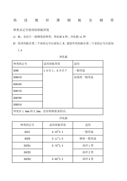
热浸镀锌薄钢板及钢带种类及记号使用的原板厚度A)板,瓦纹片一级钢卷的种类,热轧板6种,冷轧板11种B)屋顶用板在第二个表的记号后面加上R,建筑外用的板在第二个表的记号后面加上A热轧板种类的记号适用原板厚度适用SGHC 1.6以上,6.0以下一般用途SGH340 高强度一般用途SGH400SGH440SGH490SGH540厚度在1.6mm到3.2mm,没有特殊要求的话,冷轧板种类的记号适用原板厚度适用SGCC 0.25~3.2 一般用途SGCH 0.11~1.0 硬质一般用途SGCD1 0.40~2.3 深冲1类SGCD2 深冲2类SGCD3 0.60~2.3 深冲3类SGCD4 深冲4类,非时效性SGC340 0.25~3.2 高强度一般用途SGC400SGC440SGC490SGC570 0.25~2.0使用原板厚度根据买卖双方协定,在表内数据以外也可以非时效性是加工时不发生拉伸应变的特性化学成分板,瓦纹片,钢卷的化学成分符合下表,但必要时,可以添加下表以外的合金元素。
碳锰磷硫镀层镀层的种类分为非合金化和合金化两种合金化为,镀层加热后,使镀层成为铁和锌的合金镀层的记号和附着量镀层区别镀层附着记号3点平均值最小值一点最小值SGCD1,SGCD2,SGCD3,SGCD4的镀层附着量不适用于Z35,Z37,Z45,Z60,F10,F12,F18 三点平均值为,测试三次的平均值一点最小值为,测试一次的最小值板,瓦纹片及钢卷的单面最小附着量为,需在1点最小附着量的40%以上镀层的表面处理非合金化的表面处理种类及记号种类记说明号常规锌花R 镀锌的结晶凝固过程中生成的锌花微型锌花Z 将锌花极力微小化平整处理,根据客户要求进行平整处理。
镀层紧贴性弯曲180,试验片边缘7mm以内的部分不发生脱落。
客户有特殊要求的,按客户要求进行。
化学合成处理板,瓦纹片,钢卷的化学合成处理的种类和记号如下表买卖双方协定后,使用下表以外的方法也可以化学合成处理记号铬酸盐处理 C磷化处理P非铬酸盐处理NC非铬酸盐的磷化处理NP不处理M磷化处理是为了提高抗腐蚀性,磷化处理之后再进行铬酸盐处理非铬酸盐处理是不含六价铬的处理方式非铬酸盐的磷化处理是磷化处理后,进行不含六价铬的处理涂油板,瓦纹片,钢卷的涂油,有涂油记号O,无涂油记号X机械性质弯曲性拉伸特性弯曲性适用于非合金化镀层,不适用于合金化镀层原板厚度小于0.25mm拉伸特性不适用弯曲性180度弯曲,试验片边缘7mm以内的部分,不开裂、损坏拉伸特性拉伸原板厚度方向耐力拉伸强度压缩方向压缩方向或者与压缩方向垂直括弧内为参考值,使用买卖双方协定后的数值也可以括弧内为参考值,使用买卖双方协定后的数值也可以SGCD4板及钢卷,制造6个月内,加工时不发生拉伸应变尺寸及允许差标准原板厚度括弧内的数值适用于非合金化镀层Z18以上对应的镀层附着量买卖双方协定,0.65mm及0.75mm作为标准原板厚度也可。
- 1、下载文档前请自行甄别文档内容的完整性,平台不提供额外的编辑、内容补充、找答案等附加服务。
- 2、"仅部分预览"的文档,不可在线预览部分如存在完整性等问题,可反馈申请退款(可完整预览的文档不适用该条件!)。
- 3、如文档侵犯您的权益,请联系客服反馈,我们会尽快为您处理(人工客服工作时间:9:00-18:30)。
300
1000
3000
5000
Ambient temperature ˚C
Duration
6/3/03W
Viewed toward terminals
Viewed toward terminals
Viewed toward terminals
Dimensions in inches with metric equivalents in parentheses. Tolerance: ± .010"
Inrush current resistivity Non-repetitive
6/3/03W
元器件交易网
SGC-4F
RELAY ORDERING DATA SGC-4F
MODEL
05
INPUT VOLTAGE 05: 4 to 6V 12: 9.6 to 14.4V 24: 19.2 to 28.8V
D
INPUT FORM D: DC
0
OUTPUT FORM 0: Zero-cross 1: Random Phase
.787 [20.0]
4 x .157 [4.0] 4 x .028 [0.7] 4 x .016 [0.4] 4 x .028 [0.7]
4 x .157 [4.0] 4 x .016 [0.4]
PC BOARD LAYOUT
WIRING DIAGRAM
PC BOARD LAYOUT
WIRING DIAGRAM
T
TERMINAL ARRANGEMENT/ MOUNT FORM T: Pin T M: Pin M
MECHANICAL DATA
TERMINAL STYLE "T"
.945 [24.0] .256 [6.5]
TERMINAL STYLE "M"
.945 [24.0] .256 [6.5]
.787 [
4 x ø.039 [ø1.0]
.056 [1.42] .100/[2.54] GRID .171 [4.35]
4 -
3 +
2
LOAD
1
.056 [1.42] .100/[2.54] GRID .171 [4.35]
4 -
3 +
2
LOAD
1
Viewed toward terminals
元器件交易网
SGC-4F
SOLID STATE RELAY 2 AMP 250 VAC
FEATURES • Photo isolation • 600V blocking voltage • Both “Zero Voltage” and phase controllable “Random” Switching versions • High surge capability • PCB mount • UL, CUR file E43203
Output
Min. Off-state Dv/Dt at Maximum Rated Voltage Frequency Range Time Turn-on Time Turn-off Dielectric Strength
General Characteristics
Insulation Resistance Ambient Temp. Range (operating) Termination Weight Construction
Load current vs. ambient temperature characteristics
2.5 2.0
30
Inrush current (A) peak
-20 0 20 40 60 80 100
Load current (A)
20
1.5 1.0 0.5
10
0 -40
0 10
30
50 100
Voltage
05D 12D 24D 05D 12D 24D
4 to 6 VDC 9.6 to 14.4 VDC 19.2 to 28.8 VDC 4 VDC 9.6 VDC 19.2 VDC 15 mA 1 VDC 50 to 250 VAC 2A 30 A 1.5 VAC 15 mA 1.5 mA Yes 15 V/us 47 to 70 Hz 1/2 of cycle +1 ms 1/2 of cycle +1 ms 2000 VAC, 1 min. 1000MΩ min. at 500 VDC -30°C (-22°F) to 80°C (176°F) PCB terminal Approximately 5 grams Fully sealed
Input
Turn-on Voltage Current Turn-off voltage Voltage Range Current Rating (max.) Inrush Current (non repetitive) Voltage Drop (max.) Minimum Load Current Leakage Current (max.) Zero Voltage Switching
