GPTP2164中文资料
TPS51216中文资料
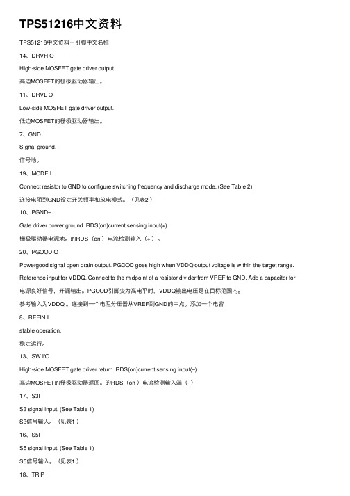
TPS51216中⽂资料TPS51216中⽂资料-引脚中⽂名称14、DRVH OHigh-side MOSFET gate driver output.⾼边MOSFET的栅极驱动器输出。
11、DRVL OLow-side MOSFET gate driver output.低边MOSFET的栅极驱动器输出。
7、GNDSignal ground.信号地。
19、MODE IConnect resistor to GND to configure switching frequency and discharge mode. (See Table 2)连接电阻到GND设定开关频率和放电模式。
(见表2 )10、PGND–Gate driver power ground. RDS(on)current sensing input(+).栅极驱动器电源地。
的RDS(on )电流检测输⼊(+ )。
20、PGOOD OPowergood signal open drain output. PGOOD goes high when VDDQ output voltage is within the target range. Reference input for VDDQ. Connect to the midpoint of a resistor divider from VREF to GND. Add a capacitor for 电源良好信号,开漏输出。
PGOOD引脚变为⾼电平时,VDDQ输出电压是在⽬标范围内。
参考输⼊为VDDQ 。
连接到⼀个电阻分压器从VREF到GND的中点。
添加⼀个电容8、REFIN Istable operation.稳定运⾏。
13、SW I/OHigh-side MOSFET gate driver return. RDS(on)current sensing input(–).⾼边MOSFET的栅极驱动器返回。
TBT8854中文资料
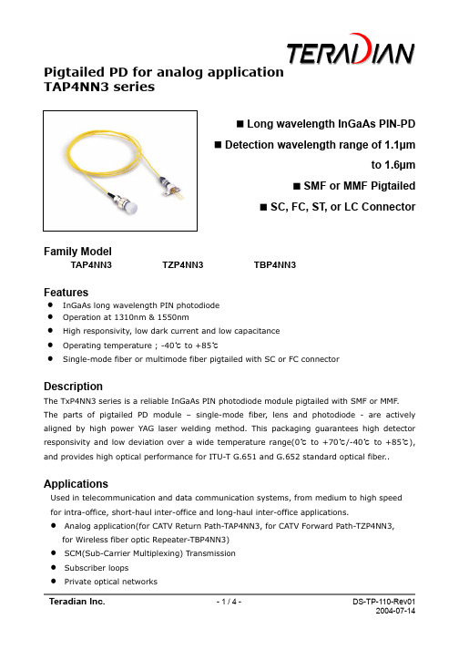
Pigtailed PD for analog applicationTAP4NN3 seriesLong wavelength InGaAs PIN-PDDetection wavelength range of 1.1µmto 1.6µmSMF or MMF PigtailedSC, FC, ST, or LC ConnectorFamily ModelTAP4NN3 TZP4NN3 TBP4NN3FeaturesInGaAs long wavelength PIN photodiodeOperation at 1310nm & 1550nmHigh responsivity, low dark current and low capacitanceOperating temperature ; -40℃ to +85℃Single-mode fiber or multimode fiber pigtailed with SC or FC connectorDescriptionThe TxP4NN3 series is a reliable InGaAs PIN photodiode module pigtailed with SMF or MMF. The parts of pigtailed PD module – single-mode fiber, lens and photodiode - are actively aligned by high power YAG laser welding method. This packaging guarantees high detector responsivity and low deviation over a wide temperature range(0℃ to +70℃/-40℃ to +85℃), and provides high optical performance for ITU-T G.651 and G.652 standard optical fiber.. ApplicationsUsed in telecommunication and data communication systems, from medium to high speedfor intra-office, short-haul inter-office and long-haul inter-office applications.Analog application(for CATV Return Path-TAP4NN3, for CATV Forward Path-TZP4NN3, for Wireless fiber optic Repeater-TBP4NN3)SCM(Sub-Carrier Multiplexing) TransmissionSubscriber loopsPrivate optical networksAbsolute Maximum RatingsParametersSymbol Unit Min.Max.RemarksAmbient Operating Temperature T op ℃ -40 85 Outdoor use Storage Temperature T stg℃-40 85Reverse Voltage V RP V - 15/20/ Reverse Current I RP mA - 3/1 / Forward CurrentI FL mA - 50/2/ Lead Soldering Temp./Time℃/sec260/10Electrical & Optical Characteristics (T op = 25℃) ParametersSymbol Condition Unit Min.Typ.Max.RemarkDetection rangeλV R =5V , R>0.75R > 0.65µm1.1 1.6Responsivity R V R =5V ,λ=1.3µm V R =5V , λ=1.5µm A/W0.800.85 0.85 0.90Dark Current I DV R =5V nA 1.0Cut-off Frequency f c -3dB, V R =5V GHz 2/3R L =50ΩReverse Breakdown VoltageV BDV R =5V , I RD =1µAV 25/0 Capacitance C V R =5V , f=1MHzpF0.6Second-Order DistortionIMD2V R =12V ,P AVG =0dBm, OMI=0.4, Note1dBc-70TAP4NN31)TZP4NN32) TBP4NN33)Third-Order Distortion IMD3 Note 1dBc -75 TZP4NN32) TBP4NN33)Back Reflection IL dB -45 Active Area Diameter∅µm75/70 45for 2GHzfor 5GHzNote1-1) TAP4NN3 : Two-tone test condition : f1=13MHz, f2=19MHz, f1±f2Note1-2) TZP4NN3 : Two-tone test condition : f1=320MHz, f2=450MHz, f1±f2, λ=1550nm per channel Note1-3) TBP4NN3 : same as the Note1-2! Handling CautionThe Photo-diode can be damaged by overvoltage and current surges. Precautions should be taken for transient power supply.This device is susceptible to damage as a result of electrostatic discharge(ESD). Take proper precautions during both handling and testingBottom view2Pin DescriptionPin No. Symbol Description 1A PDPD anode2 K PD PD cathode3 GND CasegroundOutline Diagram- TAP4xx3-xxxH-- TAP4xx3-xxxNFig.4 Pigtailed PD Package Dimensions [unit: mm]Ordering Information- 220m with 62.5/125µm MMF @1.25Gbps - 500m with 50/125µm MMF @1.25Gbps - 200m with 62.5/125µm MMF @2.125Gbps *Note 2 ; additional order information- Connector type default is SC/PC and the default length of fiber is 1mMore InformationTeradian Inc.Address 946, Dunsan-dong, Seo-gu, Daejeon, 302-120, Korea Tel +82-42-476-4800, 4803(Oversea Sales Team) Fax +82-42-476-4805Homepage e-mail sales@Com panyDevice TypeWave-length Data rate (PIN-TIA)Volt. (TIA)PinTemp. Range FiberConne ctor FlangeT A P 4N N 3 -I S NHTera dian A ;PD for CATV Return pathZ ;PD for CATV Forward Path B ;PD forwireless repeaterP ;PIN T ;PIN-TIAA ;APD 4;1.3/1.5 8;850nmN ; None0; 51Mbps 1;155Mbps 4;622Mbps 8;1.25Gbps G ;2.5GbpsN ; None 3;3.3V 5;5V 3;3pin 4;4pin (diffe- rential) 5;5pin 6;4pin (single ended)I ;Indoor Use(0~70℃) O ;Outdoor Use(-40~85℃)S ;SMFM ;MMF N ;None S ;SC F ;FC T ;ST L ;LCN ; None V ;Vertical H ; Hori- zontal。
HAT2164H中文资料
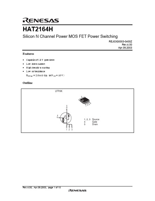
HAT2164HSilicon N Channel Power MOS FET Power SwitchingREJ03G0003-0400ZRev.4.00Apr.09.2003 Features•Capable of 4.5 V gate drive•Low drive current•High density mounting•Low on-resistanceR DS(on) = 2.5 mΩ typ. (at V GS = 10 V)OutlineAbsolute Maximum Ratings(Ta = 25°C)Item Symbol Ratings Unit Drain to source voltage V DSS30V Gate to source voltage V GSS±20V Drain current I D60A Drain peak current I D(pulse)240A Body-drain diode reverse drain current I DR60A Avalanche current I AP30A Avalanche energy E AR Note 290mJ Channel dissipation Pch30W Channel to Case Thermal Resistanceθch-C 4.17°C/W Channel temperature Tch150°C Storage temperature Tstg–55 to +150°C Notes: 1.PW ≤ 10 µs, duty cycle ≤ 1%2.Value at Tch = 25°C, Rg ≥ 50 Ω3.Tc = 25°CElectrical Characteristics(Ta = 25°C)Item Symbol Min Typ Max Unit Test ConditionsDrain to source breakdown voltage V(BR)DSS30——V I D = 10 mA, V GS = 0Gate to source breakdown voltage V(BR)GSS± 20——V I G = ±100 µA, V DS = 0 Gate to source leak current I GSS——±10µA V GS = ±16 V, V DS = 0 Zero gate voltage drain current I DSS——1µA V DS = 30 V, V GS = 0Gate to source cutoff voltage V GS(off)0.8— 2.3V V DS = 10 V, I D = 1 mA Static drain to source on state R DS(on)— 2.5 3.1mΩI D = 30 A, V GS = 10 V resistance R DS(on)— 3.0 4.4mΩI D = 30 A, V GS = 4.5 V Note4 Forward transfer admittance|y fs|78130—S I D = 30 A, V DS = 10 V Input capacitance Ciss—7600—pF V DS = 10 VOutput capacitance Coss—1050—pF V GS = 0Reverse transfer capacitance Crss—470—pF f = 1 MHzGate Resistance Rg—0.5—ΩTotal gate charge Qg—50—nc V DD = 10 VGate to source charge Qgs—22—nc V GS = 4.5 VGate to drain charge Qgd—10—nc I D = 60 ATurn-on delay time t d(on)—18—ns V GS = 10 V, I D = 30 A Rise time t r—60—ns V DD≅ 10 VTurn-off delay time t d(off)—65—ns R L = 0.33 ΩFall time t f—15—ns Rg = 4.7 ΩBody–drain diode forward voltage V DF—0.82 1.07V IF = 60 A, V GS = 0Body–drain diode reverse recovery time t rr—40—ns IF = 60 A, V GS = 0diF/ dt = 100 A/ µsNotes: 4.Pulse testMain CharacteristicsPackage DimensionsColophon 0.0。
M54HCT164中文资料
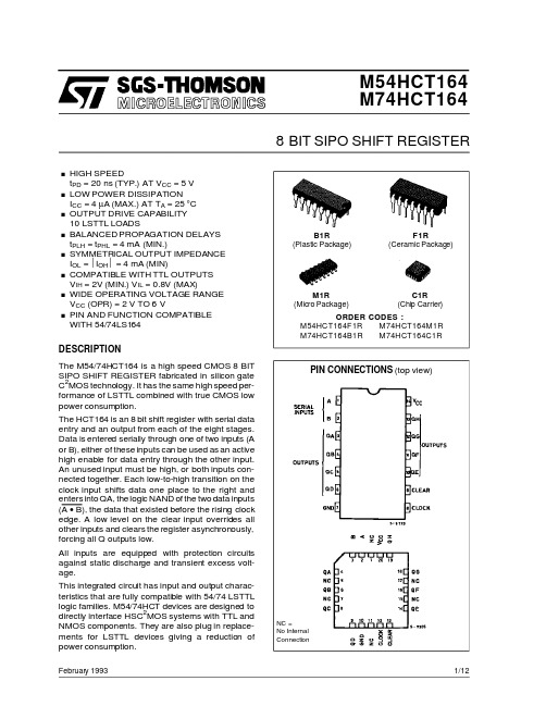
PIN No 1, 2 3, 4, 5, 6, 10, 11, 12, 13 8 9 7 14 SYMBOL A, B QA to QH NAME AND FUNCTION Data Inputs Outputs
IEC LOGIC SYMBOL
CLOCK CLEAR GND V CC
M54/M74HCT164
AC ELECTRICAL CHARACTERISTICS (C L = 50 pF, Input t r = tf = 6 ns)
Test Conditions Symbol Parameter VCC (V) 4.5 4.5 TA = 25 C 54HC and 74HC Min. Typ. 8 23 Max. 15 36
Clock Input (LOW to HIGH, Edge-triggered) Master Reset Input Ground (0V) Positive Supply Voltage
ABSOLUTE MAXIMUM RATINGS
Symbol VCC VI VO IIK IOK IO ICC or IGND PD Tstg TL Parameter Supply Voltage DC Input Voltage DC Output Voltage DC Input Diode Current DC Output Diode Current DC Output Source Sink Current Per Output Pin DC VCC or Ground Current Power Dissipation Storage Temperature Lead Temperature (10 sec) Value -0.5 to +7 -0.5 to VCC + 0.5 -0.5 to VCC + 0.5 ± 20 ± 20 ± 25 ± 50 500 (*) -65 to +150 300 Unit V V V mA mA mA mA mW
BTRS-5940A-SPG中文资料

***********************************************************************************************************************************************************************OPTOWAY TECHNOLOGY INC. No .38, Kuang Fu S. Road, Hu Kou, Hsin Chu Industrial Park, Hsin Chu, Taiwan 303BTRS-5940G / BTRS-5940-SPG / BTRS-5940AG / BTRS-5940A-SPG1490 nm TX / 1310 nm RX , 3.3V / 155 Mbps RoHS Compliant Single-Fiber Transceiver*********************************************************************************************************************************************************************FEATURESl Single Fiber Bi-Directional Transceiver l 1490 nm DFB LD Transmitter l 1310 nm Receiver l Distance Up to 40 kml Single +3.3 V Power Supply l RoHS Compliantl LVPECL Differential Inputs and Outputs l 0 to 70o C Operating : BTRS-5940G l -20 to 85o C Operating : BTRS-5940AG l Wave Solderable and Aqueous Washablel Class 1 Laser International Safety Standard IEC-60825 CompliantAPPLICATIONSl WDM 622/155 Mb/s Linksl SONET/SDH Equipment Interconnect l Fiber Channel 532 Mb/s LinksDESCRIPTIONThe BTRS-5940G series is high performance module for single fiber communications by using 1490 nm transmitter and 1310 nm receiver. The transmitter section uses a multiple quantum well 1490 nm DFB laser and is a class 1 laser compliant according to International Safety Standard IEC-825. The receiver section uses an integrated 1310 nm detector preamplifier (IDP) mounted in an optical header and a limiting post-amplifier IC. A PECL logic interface simplifies interface to external circuitry.LASER SAFETYThis single mode transceiver is a Class 1 laser product. It complies with IEC 825 and FDA 21 CFR 1040.10 and 1040.11. The transceiver must be operated within the specified temperature and voltage limits. The optical ports of the module shall be terminated with an optical connector or with a dust plug.ORDER INFORMATIONP/No.Bit Rate (Mb/s) Distance (km) TX (nm) RX (nm) Voltage (V) Package Temp (o C)TX Power (dBm) RX Sens. (dBm) RoHS Compliant BTRS-5940G 622 40 1490 DFB 1310 3.3 2X5 SC 0 to 70 0 to -5 -28 Yes BTRS-5940AG622401490 DFB13103.32X5 SC -20 to 850 to -5-28YesNote: 1. BTRS-XXXXX: 2X5 SC receptacle type package. BTRL-XXXXX: 2X5 LC receptacle type package.2. BTRX-XXXXX-APBBB is 2X5 pigtail type package with different connector, A=S is SC connector, A=F is FC connector, A=T is ST connector, A=L is LC connector, A=M is MU connector; BBB is the length of fiber in cm.Absolute Maximum RatingsParameterSymbol Min Max Units NotesStorage Temperature Tstg -40 85 o COperating Temperature Topr 0 -20 70 85 o CBTRS-5940G BTRS-5940AGSoldering Temperature --- 260 oC 10 seconds on leads only Power Supply Voltage Vcc 0 4.5 V Input Voltage --- GND Vcc VOutput CurrentIout30mARecommended Operating ConditionsParameterSymbol Min Typ Max Units / NotesPower Supply Voltage Vcc 3.13 3.3 3.47 VOperating Temperature Topr 0 -20 70 85 oC / BTRS-5940G oC / BTRS-5940AGData Rate50 622 650 Mb/s Power Supply CurrentIcc260mATransmitter Specifications (0o C < Topr < 70o C, 3.13V < Vcc < 3. 47V)Parameter Symbol Min Typ Max Units NotesOpticalOptical Transmit Power Po -5 0 dBm 1Output Center Wavelength λ1480 1500 nmOutput Spectrum Width σλ 1 nm -20 dB Width Extinction Ratio E R10 dBOutput Eye Compliant with Bellcore TR-NWT-000253 and ITU recommendation G.957Optical Rise Time t r 1.2 ns 10% to 90% Values Optical Fall Time t f 1.2 ns 10% to 90% Values Relative Intensity Noise RIN -116 dB/HzTotal Jitter TJ 0.55 ns 2ElectricalData Input Current – Low I IL-350 µAData Input Current – High I IH350 µADifferential Input Voltage V IH - V IL300 1600 mVData Input Voltage – Low V IL - V CC-2.0 -1.58 V 3Data Input Voltage -- High V IH - V CC-1.1 -0.74 V 3Disable Input Voltage -- Low V TDIS,L0 0.8 V TX Output Enabled Disable Input Voltage -- High V TDIS,H Vcc – 1.3 Vcc V TX Ouput DisabledShut Off Time for TxDis t DIS 1 msNotes: 1. Output power is power coupled into a 9/125 µm single mode fiber.2. Measured with a 223-1 PRBS with 72 ones and 72 zeros.3. These inputs are compatible with 10K, 10KH and 100K ECL and LVPECL inputs.Receiver Specifications(0o C < Topr < 70o C, 3.13 V < Vcc < 3. 47V)Parameter Symbol Min Typ Max Units NotesOpticalSensitivity--- --- --- -28 dBm 1Maximum Input Power Pin -5 --- --- dBmSignal Detect -- Asserted Pa --- --- -28 dBm Transition: low to high Signal Detect -- Deasserted Pd -42 --- --- dBm Transition: high to low Signal detect -- Hysteresis 1.0 --- 4.0 dBWavelength of Operation 1260 1360 nm 2Optical Return Loss ORL 14 dBElectricalData Output Voltage – Low V OL - V CC-2.0 -1.58 V 3Data Output Voltage – High V OH - V CC-1.1 -0.74 V 3SD Output Voltage -- Low V OL - V CC-2.0 -1.58 V 3SD Output Voltage -- High V OH - V CC-1.1 -0.74 V 3Signal Detect Assert Time AS MAX100 µs OFF to ONSignal Detect Deassert Time ANS MAX300 µs ON to OFF Notes: 1. Minimum sensitivity and saturation levels at BER 1E-10 for a 223-1 PRBS with 72 ones and 72 zeros.2. At least 30 dB optical isolation for the wavelength 1480 to 1580 nm.3. These outputs are compatible with 10K, 10KH and 100K ECL and LVPECL outputs.********************************************************************************************************************************************************************* OPTOWAY TECHNOLOGY INC. No.38, Kuang Fu S. Road, Hu Kou, Hsin Chu Industrial Park, Hsin Chu, Taiwan 303 Tel: 886-3-5979798 Fax: 886-3-5979737********************************************************************************************************************************************************************* OPTOWAY TECHNOLOGY INC. No.38, Kuang Fu S. Road, Hu Kou, Hsin Chu Industrial Park, Hsin Chu, Taiwan 303 Tel: 886-3-5979798 Fax: 886-3-5979737RECOMMENDED CIRCUIT SCHEMATIC1)Recommended DC Coupled Interface Circuit2)Recommended AC Coupled Interface Circuit********************************************************************************************************************************************************************* OPTOWAY TECHNOLOGY INC. No.38, Kuang Fu S. Road, Hu Kou, Hsin Chu Industrial Park, Hsin Chu, Taiwan 303 Tel: 886-3-5979798 Fax: 886-3-5979737。
SSM2164中文资料

SSM2164 Min Typ Max
AUDIO SIGNAL PATH Noise Headroom Total Harmonic Distortion
Channel Separation Unity Gain Bandwidth Slew Rate Input Bias Current Output Offset Current Output Compliance
Model
SSM2164P SSM2164S
SSM2164
ORDERING GUIDE
Temperature Range
–40°C to +85°C –40°C to +85°C
Package
Package
Description Options
Plastic DIP N-16 Narrow SOIC R-16A
Output Short Circuit Duration to GND . . . . . . . . . Indefinite Storage Temperature Range . . . . . . . . . . . . –65°C to +150°C Operating Temperature Range . . . . . . . . . . . . . –40°C to +85°C Junction Temperature Range . . . . . . . . . . . . –65°C to +150°C Lead Temperature Range (Soldering 60 sec) . . . . . . . . +300°C
CF = 10 pF CF = 10 pF
VIN = 0
HD74ALVCH162244中文资料

1OE 1 1Y1 2 1Y2 3 GND 4 1Y3 5 1Y4 6 VCC 7 2Y1 8 2Y2 9 GND 10 2Y3 11 2Y4 12 3Y1 13 3Y2 14 GND 15 3Y3 16 3Y4 17 VCC 18 4Y1 19 4Y2 20 GND 21 4Y3 22 4Y4 23 4OE 24
—
0.4
IOL = 4 mA, VIL = 0.7 V
2.3
—
0.55
IOL = 6 mA, VIL = 0.7 V
3.0
—
0.55
IOL = 6 mA, VIL = 0.8 V
2.7
—
0.6
IOL = 8 mA, VIL = 0.8 V
3.0
—
0.8
IOL = 12 mA, VIL = 0.8 V
Features
• VCC = 2.3 V to 3.6 V • Typical VOL ground bounce < 0.8 V (@VCC = 3.3 V, Ta = 25°C) • Typical VOH undershoot > 2.0 V (@VCC = 3.3 V, Ta = 25°C) • High output current ±12 mA (@VCC = 3.0 V) • Bus hold on data inputs eliminates the need for external pullup / pulldown resistors • All outputs have equivalent 26 Ω series resistors, so no external resistors are required.
Item
XQR17V16VQ44N中文资料
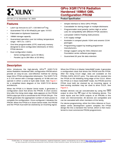
© 2003 Xilinx, Inc. All rights reserved. All Xilinx trademarks, registered trademarks, patents, and disclaimers are as listed at /legal.htm .All other trademarks and registered trademarks are the property of their respective owners. All specifications are subject to change without notice.Features•Latch-Up Immune to LET >120 MeV/cm 2/mg •Guaranteed TID of 50 kRad(Si) per spec 1019.5•Fabricated on Epitaxial Substrate •16Mbit storage capacity•Guaranteed operation over full military temperature range: –55°C to +125°C•One-time programmable (OTP) read-only memory designed to store configuration bitstreams of Xilinx FPGA devices•Dual configuration modes -Serial configuration (up to 33Mb/s)-Parallel (up to 264Mb/s at 33MHz)•Simple interface to Xilinx QPro FPGAs•Cascadable for storing longer or multiple bitstreams •Programmable reset polarity (active High or active Low) for compatibility with different FPGA solutions •Low-power CMOS Floating Gate process • 3.3V supply voltage•Available in compact plastic VQ44 and ceramic CC44 packages•Programming support by leading programmer manufacturers.•Design support using the Xilinx Alliance and Foundation series software packages.•Guaranteed 20 year life data retentionDescriptionXilinx introduces the high-density QPro™ XQR17V16series Radiation Hardened QML configuration PROM which provide an easy-to-use, cost-effective method for storing large Xilinx FPGA configuration bitstreams. The XQR17V16is a 3.3V device with a storage capacity of 16Mb and can operate in either a serial or byte wide mode. See Figure 1for a simplified block diagram of the XQR17V16 device architecture.When the FPGA is in Master Serial mode, it generates a configuration clock that drives the PROM. A short access time after the rising clock edge, data appears on the PROM DATA output pin that is connected to the FPGA DIN pin. The FPGA generates the appropriate number of clock pulses to complete the configuration. Once configured, it disables the PROM. When the FPGA is in Slave Serial mode, the PROM and the FPGA must both be clocked by an incoming signal.When the FPGA is in Master SelectMAP mode, it generates a configuration clock that drives the PROM and the FPGA.After the rising CCLK edge, data are available on the PROMs DATA (D0-D7) pins. The data will be clocked into the FPGA on the following rising edge of the CCLK. When the FPGA is in Slave SelectMAP mode, the PROM and the FPGA must both be clocked by an incoming signal. A free-running oscillator may be used to drive CCLK. See Figure 2.Multiple devices can be concatenated by using the CEO output to drive the CE input of the following device. The clock inputs and the DATA outputs of all PROMs in this chain are interconnected. All devices are compatible and can be cascaded with other members of the family.For device programming, either the Xilinx Alliance or Foun-dation series development system compiles the FPGA design file into a standard Hex format, which is then trans-ferred to most commercial PROM programmers.QPro XQR17V16 Radiation Hardened 16Mbit QML Configuration PROMDS126 (v1.0) December 18, 2003Product SpecificationPin DescriptionDATA[0:7]Data output is in a high-impedance state when either CE or OE are inactive. During programming, the D0 pin is I/O. Note that OE can be programmed to be either active High or active Low.CLKEach rising edge on the CLK input increments the internal address counter, if both CE and OE are active.RESET/OEWhen High, this input holds the address counter reset and puts the DATA output in a high-impedance state. The polar-ity of this input pin is programmable as either RESET/OE or OE/RESET. To avoid confusion, this document describes the pin as RESET/OE, although the opposite polarity is pos-sible on all devices. When RESET is active, the address counter is held at “0”, and puts the DATA output in a high-impedance state. The polarity of this input is program-mable. The default is active High RESET, but the preferred option is active Low RESET, because it can connected to the FPGAs INIT pin and a pullup resistor.The polarity of this pin is controlled in the programmer inter-face. This input pin is easily inverted using the Xilinx HW-130 Programmer. Third-party programmers have differ-ent methods to invert this pin.CEWhen High, this pin disables the internal address counter, puts the DATA output in a high-impedance state, and forces the device into low-I CC standby mode.CEOChip Enable output, to be connected to the CE input of the next PROM in the daisy chain. This output is Low when the CE and OE inputs are both active AND the internal address counter has been incremented beyond its Terminal Count (TC) value. In other words: when the PROM has been read, CEO will follow CE as long as OE is active. When OE goes inactive, CEO stays High until the PROM is reset. Note that OE can be programmed to be either active High or active Low.Figure 1: Simplified Block Diagram for XQR17V16 (does not show programming circuit)BUSY (XQR17V16 only)If BUSY pin is floating, the user must program the BUSY bit which will cause BUSY pin to be internally tied to apull-down resistor. When asserted High, output data are held and when BUSY pin goes Low, data output will resume.V PPProgramming voltage. No overshoot above the specified max voltage is permitted on this pin. For normal read oper-ation, this pin must be connected to V CC. Failure to do so may lead to unpredictable, temperature-dependent opera-tion and severe problems in circuit debugging. Do not leave V PP floating!V CC and GNDPositive supply and ground pins.PROM Pinouts for XQR17V16(Pins not listed are “no connect”)CapacityControlling PROMsConnecting the FPGA device with the PROM.•The DATA output(s) of the PROM(s) drives the D IN input of the lead FPGA device.•The Master FPGA CCLK output drives the CLK input(s) of the PROM(s).•The CEO output of a PROM drives the CE input of the next PROM in a daisy chain (if any).•The RESET/OE input of all PROMs is best driven by the INIT output of the lead FPGA device. Thisconnection assures that the PROM address counter is reset before the start of any (re)configuration, evenwhen a reconfiguration is initiated by a V CC glitch. •The PROM CE input is best connected to the FPGA DONE pin(s) and a pullup resistor. CE can also bepermanently tied Low, but this keeps the DATA output active and causes an unnecessary supply current of15mA maximum.•SelectMAP mode is similar to Slave Serial mode. The DATA is clocked out of the PROM one byte per CCLK instead of one bit per CCLK cycle. See FPGA datasheets for special configuration requirements.FPGA Master Serial Mode SummaryThe I/O and logic functions of the Configurable Logic Block (CLB) and their associated interconnections are estab-lished by a configuration program. The program is loaded either automatically upon power up, or on command, depending on the state of the three FPGA mode pins. In Master Serial mode, the FPGA automatically loads the con-figuration program from an external memory. The Xilinx PROMs have been designed for compatibility with the Mas-ter Serial mode.Upon power-up or reconfiguration, an FPGA enters the Master Serial mode whenever all three of the FPGAPin Name44-pin VQFP44-pin CLCC BUSY2430D0402D12935D2424D32733D4915D52531D61420D71925CLK435 RESET/OE(OE/RESET)1319CE1521GND6, 18, 28, 37, 413, 12, 24, 34, 43 CEO2127V PP3541V CC8, 16, 17, 26, 36,3814, 22, 23, 32,42, 44Device Configuration BitsXQR17V1616,777,216Xilinx FPGAs and Compatible PROMsDevice Configuration Bits XQR17V16(s)XQR2V10004,082,6561XQR2V300010,494,4321XQR2V600021,849, 5682XQVR3001,751,8081XQVR6003,607,9681XQVR10006,127,7441mode-select pins are Low (M0=0, M1=0, M2=0). Data is read from the PROM sequentially on a single data line. Syn-chronization is provided by the rising edge of the temporary signal CCLK, which is generated during configuration. Master Serial Mode provides a simple configuration inter-face. Only a serial data line, two control lines, and a clock line are required to configure an FPGA. Data from the PROM is read sequentially, accessed via the internal address and bit counters which are incremented on every valid rising edge of CCLK.If the user-programmable, dual-function DIN pin on the FPGA is used only for configuration, it must still be held at a defined level during normal operation. The Xilinx FPGA families take care of this automatically with an on-chip default pull-up/down resistor or keeper circuit. Cascading Configuration PROMsFor multiple FPGAs configured as a daisy-chain, or for future FPGAs requiring larger configuration memories, cas-caded PROMs provide additional memory. After the last bit from the first PROM is read, the next clock signal to the PROM asserts its CEO output Low and disables its DATA line. The second PROM recognizes the Low level on its CE input and enables its DATA output. See Figure2.After configuration is complete, the address counters of all cascaded PROMs are reset if the FPGA PROGRAM pin goes Low, assuming the PROM reset polarity option has been inverted.Figure 2: (a) Master Serial Mode (b) Virtex SelectMAP Mode (dotted lines indicates optional connection)Standby ModeThe PROM enters a low-power standby mode whenever CE is asserted High. The output remains in a high imped-ance state regardless of the state of the OE input.ProgrammingThe devices can be programmed on programmers supplied by Xilinx or qualified third-party vendors. The user must ensure that the appropriate programming algorithm and the latest version of the programmer software are used. The wrong choice can permanently damage the device.Radiation TolerancesTable 1: Truth Table for XQ17V00 Control InputsControl Inputs Internal AddressOutputs RESET CE DATA CEO I CC Inactive Low If address < TC (1): increment If address > TC (1): don’t changeActive High-Z High Low Active Reduced Active Low Held reset High-Z High Active Inactive High Not changing High-Z High Standby ActiveHighHeld resetHigh-ZHighStandbyNotes:1.The XQ17V00 RESET input has programmable polarity1.TC = Terminal Count = highest address value. TC + 1 = address 0.Table 2: Guaranteed Radiation Tolerance Specifications (1)Symbol DescriptionMin Max Units TID Total Ionizing Dose for data retention and data output port read (configuration) operations -50krad(Si)SEL Single Event Latch-Up(No Latch-Up observed for LET > 120 MeV-mg/cm 2)-0cm 2SEUStatic Memory Cell Saturation Bit Cross-Section (No Upset observed for LET > 120 MeV-mg/cm 2)-cm 2Notes:1.For more information on dynamic SEU error rates please see the SEU test reports at /milaeroAbsolute Maximum RatingsOperating Conditions (3.3V Supply)DC Characteristics Over Operating ConditionSymbol DescriptionConditions Units V CC Supply voltage relative to GND –0.5 to +7.0V V PP Supply voltage relative to GND –0.5 to +12.5V V IN Input voltage relative to GND –0.5 to V CC +0.5V V TS Voltage applied to High-Z output –0.5 to V CC +0.5V T STG Storage temperature (ambient)–65 to +150°C T SOL Maximum soldering temperature (10s @ 1/16 in.)+260°C T JJunction temperatureCeramic +150°C Plastic+125°CNotes:1.Stresses beyond those listed under Absolute Maximum Ratings may cause permanent damage to the device. These are stressratings only, and functional operation of the device at these or any other conditions beyond those listed under Operating Conditions is not implied. Exposure to Absolute Maximum Ratings conditions for extended periods of time may affect device reliability.Symbol DescriptionMin Max Units V CC (1)Supply voltage relative to GND (T C = –55°C to +125°C)Ceramic 3.0 3.6V Supply voltage relative to GND (T J = –55°C to +125°C)Plastic3.0 3.6V T VCCV CC rise time from 0V to nominal voltage1.050msNotes:1.During normal read operation V PP must be connected to V CC.2.At power up, the device requires the V CC power supply to monotonically rise from 0V to nominal voltage within the specified V CC risetime. If the power supply cannot meet this requirement, then the device may not power-on-reset properly.Symbol DescriptionMin Max Units V IH High-level input voltage 2V CC V V IL Low-level input voltage00.8V V OH High-level output voltage (I OH = –3 mA) 2.4-V V OL Low-level output voltage (I OL = +3 mA)-0.4V I CCA Supply current, active mode (at maximum frequency) -100mA I CCS Supply current, standby mode -1mA I L Input or output leakage current–1010µA C IN Input capacitance (V IN = GND, f = 1.0 MHz)-15pF C OUTOutput capacitance (V IN = GND, f = 1.0 MHz)-15pFAC Characteristics Over Operating Condition for XQR17V16Symbol Description Min Max Units T OE OE to data delay-15ns T CE CE to data delay-20ns T CAC CLK to data delay(2)-20ns T DF CE or OE to data float delay(3,4)-35ns T OH Data hold from CE, OE, or CLK(4)0-ns T CYC Clock periods50-ns T LC CLK Low time(4)25-ns T HC CLK High time(4)25-ns T SCE CE setup time to CLK (to guarantee proper counting)25-ns T HCE CE hold time to CLK (to guarantee proper counting)0-ns T HOE OE hold time (guarantees counters are reset)25-ns T SBUSY BUSY setup time5-ns T HBUSY BUSY hold time5-ns Notes:1.AC test load = 50 pF.2.When BUSY = 0.3.Float delays are measured with 5 pF AC loads. Transition is measured at ±200 mV from steady state active levels.4.Guaranteed by design, not tested.5.All AC parameters are measured with V IL = 0.0V and V IH = 3.0V.AC Characteristics Over Operating Condition When CascadingSymbol DescriptionMin Max Units T CDF CLK to data float delay (2,3)-50ns T OCK CLK to CEO delay (3)-30ns T OCE CE to CEO delay (3)-35ns T OOERESET/OE to CEO delay (3)-30nsNotes:1.AC test load = 50 pF2.Float delays are measured with 5 pF AC loads. Transition is measured at ±200 mV from steadystate active levels.3.Guaranteed by design, not tested.4.All AC parameters are measured with V IL = 0.0V and V IH= 3.0V.Ordering InformationRevision HistoryThe following table shows the revision history for this document.Date Version Revision12/15/031.0Initial Xilinx release.XQR17V16 CC44 VManufacturing GradePackage TypeDevice NumberDevice Ordering OptionsDevice Type PackageGradeFlowTempXQR17V16CC4444-pin Ceramic Chip Carrier Package M M-Grade Military Ceramic T C = –55°C to +125°CVQ4444-pin Plastic Thin Quad Flat PackageV QPRO-PLUS N Class NMilitary Plastic T J = –55°C to +125°CRQPRO+PLUS PEMValid Ordering CombinationsM Grade V Grade N Grade R Grade XQR17V16CC44MXQR17V16CC44VXQR17V16VQ44NXQR17V16VQ44R。
PS21964-AT中文资料
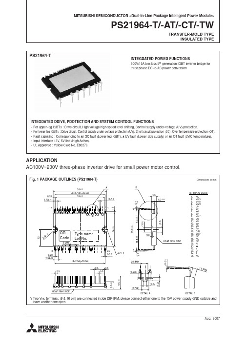
High-side input (PWM) (3V, 5V line)(Note 1, 2)
Input signal conditioning Level shifter
Protection circuit (UV)
Input signal conditioning Level shifter
Input signal conditioning Level shifter
25 8-0.6 4-C1.2
0.5 0.5 0.5 (2.656)
(0~5°)
(0~5°)
0.4
1.5 M
IN
±0.5
5.5±0.5
(1.2) (2.756) DETAIL A
HEAT SINK SIDE
(1.2)
9.5
DETAIL B
*) Two VNC terminals (9 & 16 pin) are connected inside DIP-IPM, please connect either one to the 15V power supply GND outside and leave another one open.
HEAT SINK SIDE
(1.2)
DETAIL B
*) Two VNC terminals (9 & 16 pin) are connected inside DIP-IPM, please connect either one to the 15V power supply GND outside and leave another one open.
Fig. 5 INTERNAL FUNCTIONS BLOCK DIAGRAM (TYPICAL APPLICATION EXAMPLE)
MAX2644EXT+T;中文规格书,Datasheet资料
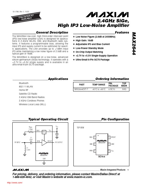
________________________Applicatห้องสมุดไป่ตู้ons
Bluetooth 802.11 WLAN Home RF Satellite CD Radio 2.4GHz ISM Band Radios 2.4GHz Cordless Phones Wireless Local Loop (WLL)
/
2.4GHz SiGe, High IP3 Low-Noise Amplifier MAX2644
Typical Operating Characteristics
(PRFIN = -30dBm, ZS = ZL = 50Ω, VCC = +3.0V, fRFIN = 2450MHz, RBIAS = 1.2kΩ, TA = +25°C, unless otherwise noted.)
MAX2644
The MAX2644 low-cost, high third-order intercept point (IP3) low-noise amplifier (LNA) is designed for applications in 2.4GHz WLAN, ISM, and Bluetooth radio systems. It features a programmable bias, allowing the input IP3 and supply current to be optimized for specific applications. The LNA provides up to +1dBm input IP3 while maintaining a low noise figure of 2.0dB and a typical gain of 16dB. The MAX2644 is designed on a low-noise, advanced silicon-germanium (SiGe) technology. It operates with a +2.7V to +5.5V single supply and is available in an ultra-small 6-pin SC70 package.
74VCX16244G资料

© 2005 Fairchild Semiconductor Corporation
DS012168
元Logic Symbol
Pin Descriptions
Pin Names OEn I0–I15 O0–O15 NC Description Output Enable Input (Active LOW) Inputs Outputs No Connect
Connection Diagrams
Pin Assignment for TSSOP
FBGA Pin Assignments
1 A B C D E F G H J O0 O2 O4 O6 O8 O10 O12 O14 O15 2 NC O1 O3 O5 O7 O9 O11 O13 NC 3 OE1 NC VCC GND GND GND VCC NC OE4 4 OE2 NC VCC GND GND GND VCC NC OE3 5 NC I1 I3 I5 I7 I9 I11 I13 NC 6 I0 I2 I4 I6 I8 I10 I12 I14 I15
Logic Diagram
3
元器件交易网
74VCX16244
Absolute Maximum Ratings(Note 4)
Supply Voltage (VCC) DC Input Voltage (VI) Output Voltage (VO) Outputs 3-STATED Outputs Active (Note 5) DC Input Diode Current (IIK) VI 0V DC Output Diode Current (IOK) VO 0V VO ! VCC DC Output Source/Sink Current (IOH/IOL) DC VCC or GND Current per Supply Pin (ICC or GND) Storage Temperature Range (TSTG)
TLP3526中文资料

1.0
1.4
1.8
2.2
2.6
Pulse forward voltage VFP (V)
4
2002-09-25
元器件交易网
Trigger LED current IFT (arbitrary unit)
Peak off-state current IDRM (arbitrary unit)
元器件交易网
TL(Ta = 25°C)
Characteristic
Symbol
Rating
Unit
Forward current
Forward current derating (Ta ≥ 53°C)
LE D
Peak forward current (100µs pulse, 100pps)
Characteristic Trigger LED current Capacitance (input to output) Isolation resistance
Isolation voltage
Fig.1: dv / dt test circuit
Symbol IFT CS RS
BVS
Test Condition
VT = 6V VS = 0, f = 1MHz VS = 500V AC, 1 minute AC, 1 second, in oil DC, 1 minute, in oil
Min.
―
― 5×10¹⁰ 2500
― ―
Typ.
―
1.5 1014 ― 5000 5000
Max. 10 ―
― ― ― ―
1 5 125 600 1.0 0.7 -14.3
1949144中文资料

Extract from the online catalogMSTB 2,5/20-STF-5,08 AUOrder No.: 1949144http://eshop.phoenixcontact.de/phoenix/treeViewClick.do?UID=1949144Plug component, nominal current: 12 A, rated voltage: 250 V, pitch:5.08 mm, no. of positions: 20, type of connection: Screw connectionhttp:// Please note that the data given here has been taken from theonline catalog. For comprehensive information and data, please refer to the user documentation. The General Terms and Conditions of Use apply to Internet downloads.Certificates / ApprovalsApproval logoCSANominal voltage U N 300 V Nominal current I N 10 A AWG/kcmil28-12CULNominal voltage U N300 VNominal current I N10 AAWG/kcmil30-12ULNominal voltage U N300 VNominal current I N10 AAWG/kcmil30-12Certification CB, CSA, CUL, UL, VDE-PZIAccessoriesItem Designation DescriptionBridges1733172EBP 3- 5Insertion bridge, fully insulated, for plug connectors with 5.0 or5.08 mm pitch, no. of positions: 31733185EBP 4- 5Insertion bridge, fully insulated, for plug connectors with 5.0 or5.08 mm pitch, no. of positions: 41733198EBP 5- 5Insertion bridge, fully insulated, for plug connectors with 5.0 or5.08 mm pitch, no. of positions: 51733208EBP 6- 5Insertion bridge, fully insulated, for plug connectors with 5.0 or5.08 mm pitch, no. of positions: 6General1733169EBP 2- 5Insertion bridge, fully insulated, for plug connectors with 5.0 or5.08 mm pitch, no. of positions: 2Marking1051993B-STIFT Marker pen, for manual labeling of unprinted Zack strips, smear-proof and waterproof, line thickness 0.5 mm0804293SK 5,08/3,8:FORTL.ZAHLEN Marker card, printed horizontally, self-adhesive, 12 identicaldecades marked 1-10, 11-20 etc. up to 91-(99)100, sufficient for120 terminal blocks0805085SK 5,08/3,8:SO Marker card, special printing, self-adhesive, labeled acc. tocustomer requirements, 12 identical marker strips per card, max.25-position labeling per strip, color: white0803906SK U/3,8 WH:UNBEDRUCKT Unprinted marker cards, DIN A4 format, pitch as desired, self-adhesive, with 40 stamped marker strips, 185 mm strip length, canbe labeled with the CMS system or manually with the M-PEN 0811228X-PEN 0,35Marker pen without ink cartridge, for manual labeling of markers,labeling extremely wipe-proof, line thickness 0.35 mmPlug/Adapter1734634CP-MSTB Coding profile, is inserted into the slot on the plug or invertedheader, red insulating materialTools1205053SZS 0,6X3,5Screwdriver, bladed, matches all screw terminal blocks up to 4.0mm² connection cross section, blade: 0.6 x 3.5 mm, without VDEapprovalAdditional productsItem Designation DescriptionGeneral1803138MSTBVK 2,5/20-GF-5,08Header, nominal current: 12 A, rated voltage: 320 V, pitch: 5.08mm, no. of positions: 20, mounting: Mounting rail1788525MVSTBU 2,5/20-GFB-5,08Header, nominal current: 12 A, rated voltage: 320 V, pitch: 5.08mm, no. of positions: 20, mounting: Direct mounting3002034UK 3-MSTB-5,08Modular terminal blocks with plug entry, cross section: 0.2 - 2.5mm², AWG: 30 - 12, width: 5.1 mm, color: gray3002076UK 3-MVSTB-5,08Modular terminal blocks with plug entry, cross section: 0.2 - 2.5mm², AWG: 26 - 12, width: 5.1 mm, color: gray3002102UK 3-MVSTB-5,08-LA 24RD Modular terminal block with plug entry, nominal current: 12 A,rated voltage: 320 V, pitch: 5.08 mm, no. of positions: 1, mounting:mounting rail, with red light indicator, voltage light indicator: 24 VAC/DC, current light indicator: 3.3 mA3002063UK 3-MVSTB-5,08/EK Modular terminal blocks with plug entry, cross section: 0.2-2.5mm², AWG: 26-12, width: 5.1 mm, color: blue3002131UK 3D-MSTBV-5,08Modular terminal blocks with vertical plug entry, cross section: 0.2- 2.5 mm, AWG: 30 - 12, width: 5.1 mm, color: gray3002144UK 3D-MSTBV-5,08-LA 24RD Modular terminal block with vertical plug entry, color: Gray, withred light indicator, voltage light indicator: 24 V AC/DC, current lightindicator: 3.3 mA3002173UK 3D-MSTBV-5,08/EK Modular terminal blocks with plug entry, cross section: 0.2 - 2.5mm², AWG: 30 - 12, width: 5.1 mm, color: blue2770888UKK 3-MSTB-5,08Modular terminal blocks with 2 horizontal plug entries, crosssection: 0.2 - 2.5 mm, AWG: 30 - 12, width: 5.1 mm, color: gray 1876615UKK 3-MSTB-5,08-PE Ground terminal block, with 2 horizontal plug entries, nominalcurrent: 12 A, rated voltage: 320 V, pitch: 5.08 mm, no. ofpositions: 1, mounting: mounting rail.1788101UMSTBVK 2,5/20-GF-5,08Header, nominal current: 12 A, rated voltage: 320 V, pitch: 5.08mm, no. of positions: 20, mounting: Mounting rail1873016ZFKK 1,5-MSTBV-5,08Modular terminal blocks with plug entry, cross section: 0.2 - 1.5mm², width: 5.1 mm, color: grayAddressPHOENIX CONTACT GmbH & Co. KGFlachsmarktstr. 832825 Blomberg,GermanyPhone +49 5235 3 00Fax +49 5235 3 41200http://www.phoenixcontact.de© 2008 Phoenix ContactTechnical modifications reserved;。
74HC164中文资料参数
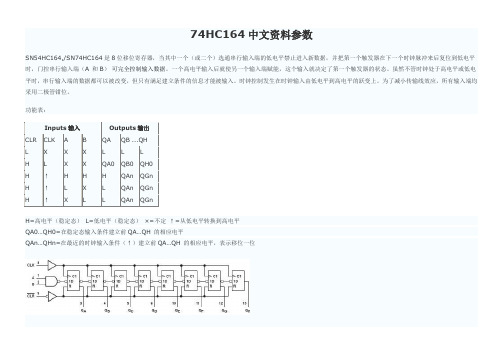
74HC164中文资料参数SN54HC164,/SN74HC164是8位移位寄存器,当其中一个(或二个)选通串行输入端的低电平禁止进入新数据,并把第一个触发器在下一个时钟脉冲来后复位到低电平时,门控串行输入端(A 和B)可完全控制输入数据。
一个高电平输入后就使另一个输入端赋能,这个输入就决定了第一个触发器的状态。
虽然不管时钟处于高电平或低电平时,串行输入端的数据都可以被改变,但只有满足建立条件的信息才能被输入。
时钟控制发生在时钟输入由低电平到高电平的跃变上。
为了减小传输线效应,所有输入端均采用二极管钳位。
功能表:Inputs输入Outputs输出CLR CLK A B QA QB ...QHL X X X L L LH L X X QA0QB0QH0H↑H H H QAn QGnH↑L X L QAn QGnH↑X L L QAn QGnH=高电平(稳定态)L=低电平(稳定态)×=不定↑=从低电平转换到高电平QA0…QH0=在稳定态输入条件建立前QA…QH 的相应电平QA n…QHn=在最近的时钟输入条件(↑)建立前QA…QH 的相应电平,表示移位一位图1 逻辑图(正逻辑)图2 引脚图Absolute Maximum Ratings绝对最大额定值Supply voltage range, 电源电压范围VCC–0.5 V to 7V Input clamp current, 输入钳位电流IIK (VI < 0 or VI > VCC) (see Note 1)±20 mA Output clamp current,输出钳位电流IOK (VO < 0 or VO > VCC) (see Note 1)±20 mA Continuous output current,连续输出电流IO (VO = 0 to VCC)±25 mA Continuous current through 连续通过电流VCC or GND±50 mA封装热阻thermal impedance, θJA (see Note 2):D 封装86℃/W N 封装80℃/W NS 封装76℃/W PW 封装113℃/WStorage temperature range, Tstg储存温度范围–65℃to 150℃DC SPECIFICATIONS直流电气规格表:DC SPECIFICATIONS直流电气规格(续)IOH=–4mA 4.5 V3.984.3- 3.84- 3.7-IOH=5.2mA6 V 5.485.8- 5.34- 5.2-VOL 输出低电平电压VI=VIHorVILIOL=20μA2 V-0.0020.1-0.1-0.1V4.5 V-0.0010.1-0.1-0.16 V-0.0010.1-0.1-0.1IOL = 4mA 4.5 V-0.170.26-0.4-0.33IOL=5.2mA6 V-0.150.26-0.4-0.33II 输入漏电流VI = VCC or 0 6 V-±0.1±100-±1000-±1000nA ICC 静态电源电流VI = VCC or 0,IO = 0 6 V--8-160-80μACi 电容-2V to6V-310-10-10pF 图3 参数测量信息图4 typical clear, shift, and clear sequence典型清除、移位和清除时序应用电路:图5 LCD驱动电路图6 LED驱动电路图7 4位数码显示电路。
1971044资料
Certificates / Approvals
Approval logo
CSA Nominal voltage UN 300 V
PHOENIX CONTACT GmbH & Co. KG http://www.phoenixcontact.de
Page 1 / 3 Mar 8, 2008
元器件交易网
10 A 28-12
300 V 10 A 30-12
300 V 10 A 30-12 CSA, CUL, UL
PHOENIX CONTACT GmbH & Co. KG http://www.phoenixcontact.de
Page 2 / 3 Mar 8, 2008
元器件交易网
SMSTB 2,5/19-STF Order No.: 1971044
http://eshop.phoenixcontact.de/phoenix/treeViewClick.do?UID=1971044
Nominal current IN AWG/kcmil CUL Nominal voltage UN Nominal current IN AWG/kcmil UL Nominal voltage UN Nominal current IN AWG/kcmil Certification
元器件交易网
Extract from the online catalog
SMSTB 2,5/19-STF
Order No.: 1971044
The figure shows a 10-position version of the product
http://eshop.phoenixcontact.de/phoenix/treeViewClick.do?UID=1971044 Product notes Commercial data EAN Pack Customs tariff Weight/Piece Catalog page information 4017918931186 50 Pcs. 85366990 0.038 KG Page 129 (CC-2005) http:// Please note that the data given here has been taken from the online catalog. For comprehensive information and data, please refer to the user documentation. The General Terms and Conditions of Use apply to Internet downloads. WEEE/RoHS-compliant since: 06/17/2003
1942426资料
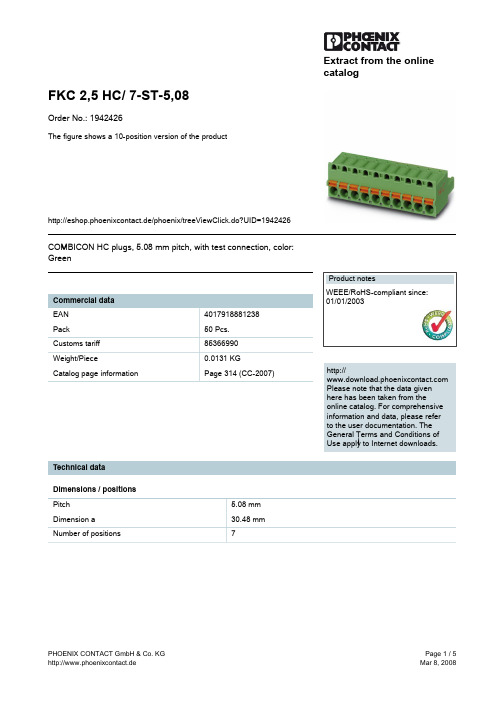
Extract from the onlinecatalogFKC 2,5 HC/ 7-ST-5,08Order No.: 1942426The figure shows a 10-position version of the producthttp://eshop.phoenixcontact.de/phoenix/treeViewClick.do?UID=1942426COMBICON HC plugs, 5.08 mm pitch, with test connection, color: Greenhttp://Please note that the data givenhere has been taken from theonline catalog. For comprehensiveinformation and data, please referto the user documentation. TheGeneral Terms and Conditions ofUse apply to Internet downloads. Technical dataDimensions / positionsPitch 5.08 mmDimension a30.48 mmNumber of positions7Technical dataInsulating material group IRated surge voltage (III/3) 4 kVRated surge voltage (III/2) 4 kVRated surge voltage (II/2) 4 kVRated voltage (III/2)320 VRated voltage (II/2)630 VConnection in acc. with standard EN-VDENominal current I N16 ANominal voltage U N250 VNominal cross section 2.5 mm2Maximum load current16 A (with 2.5 mm2 conductor cross section) Insulating material PAInflammability class acc. to UL 94V0Internal cylindrical gage A2Stripping length10 mmConnection dataConductor cross section solid min.0.2 mm2Conductor cross section solid max. 2.5 mm2Conductor cross section stranded min.0.2 mm2Conductor cross section stranded max. 2.5 mm2Conductor cross section stranded, with ferrule0.25 mm2without plastic sleeve min.Conductor cross section stranded, with ferrule2.5 mm2without plastic sleeve max.Conductor cross section stranded, with ferrule0.25 mm2with plastic sleeve min.Conductor cross section stranded, with ferrule1.5 mm2with plastic sleeve max.Conductor cross section AWG/kcmil min.24Conductor cross section AWG/kcmil max122 conductors with same cross section, stranded,0.5 mm2TWIN ferrules with plastic sleeve, min.2 conductors with same cross section, stranded,1.5 mm2TWIN ferrules with plastic sleeve, max.Certificates / ApprovalsApproval logoCULNominal voltage U N300 VNominal current I N10 AAWG/kcmil26-12ULNominal voltage U N300 VNominal current I N10 AAWG/kcmil26-12Certification CB, CUL, GOST, UL, VDE-PZIAccessoriesItem Designation DescriptionMarking0804303SK 5,08/3,8: 0-9Marker card, printed horizontally, self-adhesive, 10-section markerstrip, 12 identical decades marked 0-9, sufficient for 120 terminalblocks0804293SK 5,08/3,8:FORTL.ZAHLEN Marker card, printed horizontally, self-adhesive, 12 identicaldecades marked 1-10, 11-20 etc. up to 91-(99)100, sufficient for120 terminal blocks0805085SK 5,08/3,8:SO Marker card, special printing, self-adhesive, labeled acc. tocustomer requirements, 12 identical marker strips per card, max.25-position labeling per strip, color: white0805412SK 5,08/3,8:UNBEDRUCKT Marker cards, unprinted, with pitch divisions, self-adhesive, 10-section marker strips, 12 strips per card, can be labeled with theM-PENPlug/Adapter1734634CP-MSTB Coding profile, is inserted into the slot on the plug or invertedheader, red insulating material0201731MPS-IH BK Insulating sleeve (black), for MPS metal part to be orderedseparately (0201744)0201689MPS-IH BU Insulating sleeve (blue), for MPS metal part to be orderedseparately (0201744)0201702MPS-IH GN Insulating sleeve (green), for MPS metal part to be orderedseparately (0201744)0201728MPS-IH GY Insulating sleeve (gray), for MPS metal part to be orderedseparately (0201744)0201676MPS-IH RD Insulating sleeve (red), for MPS metal part to be orderedseparately (0201744)0201715MPS-IH VT Insulating sleeve (violet), for MPS metal part to be orderedseparately (0201744)0201663MPS-IH WH Insulating sleeve (white), for MPS metal part to be orderedseparately (0201744)0201692MPS-IH YE Insulating sleeve (yellow), for MPS metal part to be orderedseparately (0201744)0201744MPS-MT Test plug, consisting of: Metal part for 2.3 mm diameter sockethole0201647RPS Reducing plug, for transition from 4 mm diameter test plug socket,insulation: grayTools1205053SZS 0,6X3,5Screwdriver, bladed, matches all screw terminal blocks up to 4.0mm² connection cross section, blade: 0.6 x 3.5 mm, without VDEapprovalDrawingsDiagramDerating curve for: FKC 2,5 HC/..-ST with MSTBA 2,5 HC/..-GDimensioned drawingAddressPHOENIX CONTACT GmbH & Co. KGFlachsmarktstr. 832825 Blomberg,GermanyPhone +49 5235 3 00Fax +49 5235 3 41200http://www.phoenixcontact.de© 2008 Phoenix ContactTechnical modifications reserved;。
HA17084P资料
HA17082
Vout1 1 Vin(−)1 2 Vin(+)1 3
VEE 4
1
−+
2
+−
8 VCC 7 Vout2 6 Vin(−)2 5 Vin(+)2
(Top view)
HA17083
Vin(−)1 1
Vin(+)1 2
Offset Null (N2)
3
VEE 4
Offset Null (N2)
—5
20 IIB(–) |
1
Input bias current IIB
— 30 400 — 30 200 pA
1, 2
Common-mode
VCM
±10 —
—
±11 —
—
V
1
input voltage range
Maximum output Vop-p 24 27 — 24 27 — V voltage amplitude
Vout2 7
1
4
−+
−+
2
3
(Top view)
−+ −+
14 Vout4 13 Vin(−)4 12 Vin(+)4 11 VEE 10 Vin(+)3 9 Vin(−)3 8 Vout3
2
Voltage Offset Test Circuit
−
+
N1
N2
100 KΩ
VEE HA17083
HA17080 Series
HA17080 Series
HA17080A Series
Item
Symbol Min Typ Max Min Typ Max Unit Test Conditions
321499资料

/TE/bin/TE.Connect?C=1&M=BYPN&TCPN=321499&RQPN=321499
11/27/2007
元器件交易网
Receptacle Style = Straight Body Style = SOLISTRAND Barrel Type = Closed Barrel
Provide Website Feedback | Contact Customer Support
Home | Customer Support | Suppliers | Site Map | Privacy Policy | Browser Support © 2007 Tyco Electronics Corporation All Rights Reserved
Wire/Cable Type = Regular Wire Insulation = No Insulation Support = Non-Insulation Support Stud Size = 6 [M3.5] Stud Diameter (mm [in]) = 3.51 [0.138] Shape = RING-089 Heavy Duty = No Material = Copper Finish = Tin Body Related Features: Wire Range (mm [AWG]) = 3.00-6.00² [12-10] Wire Range (CMA) = 5,180 – 13,100 Barrel I.D. Min. (mm [in]) = 3.28 [0.129] Stock Thickness (mm [in]) = 1.07 [0.042]
/TE/bin/TE.Connect?C=1&M=BYPN&TCPN=321499&RQPN=321499
- 1、下载文档前请自行甄别文档内容的完整性,平台不提供额外的编辑、内容补充、找答案等附加服务。
- 2、"仅部分预览"的文档,不可在线预览部分如存在完整性等问题,可反馈申请退款(可完整预览的文档不适用该条件!)。
- 3、如文档侵犯您的权益,请联系客服反馈,我们会尽快为您处理(人工客服工作时间:9:00-18:30)。
GPTP2164
PHASE CONTROLLED SCR
High reliability operation DC power supply AC drives
VOLTAGE UP TO 1800V AVERAGE CURRENT 1645A SURGE CURRENT
27kA
BLOCKING CHARACTERISTICS Characteristic
Conditions V RRM Repetitive peak reverse voltage 1800V V RSM Non-repetitive peak reverse voltage 1900V V DRM Repetitive peak off-state voltage 1600V I DRM Repetitive peak off-state current, max.V DRM , single phase, half wave, Tj = Tjmax 50mA I RRM
Repetitive peak reverse current, max.
V RRM , single phase, half wave, Tj = Tjmax
50mA
ON-STATE CHARACTERISTICS
I T(AV)Average on-state current Sine wave,180° conduction, Th = 55 °C
1645A I T(RMS)R.M.S. on-state current Sine wave,180° conduction, Th = 55 °C
2584A I TSM Surge on-state current Non rep. half sine wave, 50 Hz, V R = 0 V, T j = T jmax
27kA I²t I² t for fusing coordination 3920kA²s V T(TO)
Threshold voltage T j = T jmax 0,84V r T
On-state slope resistance T j = T jmax
0,23m ΩV TM Peak on-state voltage, max On-state current I T =2900A , Tj = 25 °C 1,45V I H Holding current, max T j = 25 °C 300mA I L
Latching current, typ
T j = 25 °C
700mA
TRIGGERING CHARACTERISTICS
V GT Gate trigger voltage T j = 25 °C, V D = 5 V 3,5V I GT Gate trigger current T j = 25 °C, V D = 5 V 300mA V GD Non-trigger voltage
V D = 67% V RRM , T j = T jmax 0,25V P GM Peak gate power dissipation Pulse width 100 µs
150W P G(AV)Average gate power dissipation 2W I FGM Peak gate current
10A V FGM Peak gate voltage (forward)30V V RGM
Peak gate voltage (reverse)
5V
SWITCHING CHARACTERISTICS
di/dt Critical rate of rise of on-state current T j = T jmax 200A/µs dV/dt Critical rate of rise of off-state voltage T j = T jmax
500V/µs
t q
Turn-off time, typ
T j = T jmax , I T = 1000 A, di/dt = -20 A/µs µs
VR = 50 V, VD = 67% VDRM, dV/dt = 20 V/µs
THERMAL AND MECHANICAL CHARACTERISTICS
R th(j-c)Thermal resistance (junction to case)Double side cooled 0,018°C/W R th(c-h)Thermal resistance (case to heatsink)Double side cooled
0,006°C/W T jmax Max operating junction temperature 125°C T stg Storage temperature -40 / 125°C
F
Clamping force ± 10%22kN Mass
500g
Document GPTP2164T001
Value
Green Power Solutions srl
Via Greto di Cornigliano 6R - 16152 Genova , Italy
Phone: +39-010-659 1869Fax: +39-010-659 1870
Web: www.gpsemi.it E-mail: info@gpsemi.it
PHASE CONTROLLED SCR GPTP2164。
