PC4002中文资料
2SC5949中文资料(toshiba)中文数据手册「EasyDatasheet - 矽搜」
300
FE
Tc = 100°C
100 25
50 −25
30
DC电流增益^ h
10
hFE的 - 我C
5
0.03
0.1
0.3
1
3
10
30
集电极电流Ir IC / IB = 10 V
1
VCE (sat) – IC
0.5
0.3
(V)
Tc = 100°C
集电极 CE
(A)
IC max(pulsed) *
C
10 IC max(continuous)
DC operation Tc = 25°C
1 ms * 10 ms * 100 ms *
集电极电1流I
*:Single non-repetitive pulse
Tc = 25°C
Curves must be de-rated
芯片中文手册,看全文,戳
功率放大器应用
东芝晶体管硅NPN三重扩散型
2SC5949
• PC = 220W • 为了补充2SA2121
最大额定值
( TC = 25℃)
特有
集电极基极电压
集电极 - 发射极电压
发射极基极电压 集电极电流 基极电流 集电极耗散功率 结温 存储温度范围
符
评级
Unit
(-sa发0t).1射极饱和电压
V 0.05
0.03
25 −25
0.01
0.03
0.1
0.3
1
3
10
30
集电极电流I
C (A)
100
(MHz)
T
10
fT– IC
2MBI400U2B-060中文资料
Collector current : Ic [A]
IGBT Module
Collector current vs. Collector-Emitter voltage (typ.) Tj= 125°C / chip
1000
VGE=20V15V 12V 800
10V 600
400
200
0 0
8V
1
2
元器件交易网
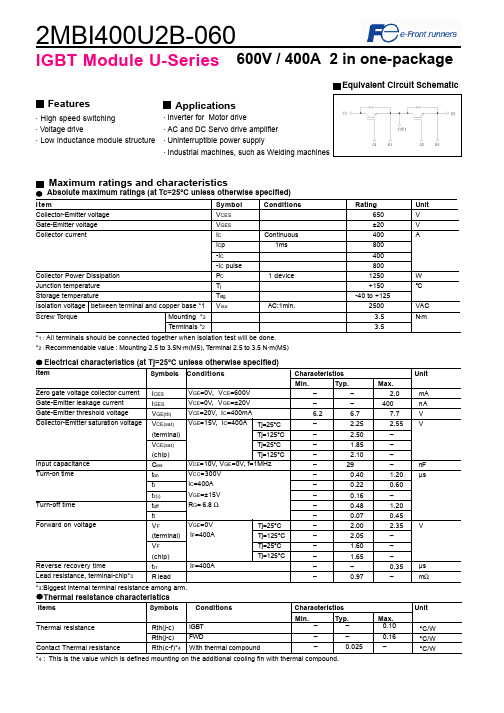
2MBI400U2B-060
IGBT Module U-Series 600V / 400A 2 in one-package
2. Equivalent circuEit quivalent Circuit Schematic
Features
· High speed switching · Voltage drive · Low inductance module structure
IGBT Module
10000
Switching time vs. Collector current (typ.) Vcc=300V, VGE=±15V, Rg=6.8Ω, Tj= 25°C
Switching time vs. Collector current (typ.) Vcc=300V, VGE=±15V, Rg=6.8Ω, Tj=125°C
Collector current : Ic [A]
600
10V
400
200
0 0
8V
1
2
3
4
5
Collector-Emitter voltage : VCE [V]
Collector current : Ic [A]
PC400光耦资料
2
Ambient temperature T a ( ˚C )
5 10 20 50 Low level output current I OL ( mA )
100
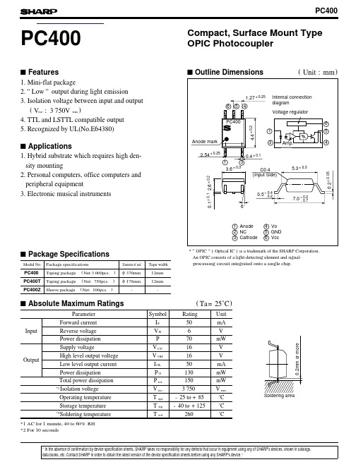
PC400
Fig. 7 Low Level Output Voltage vs. Ambient Temperature
0.5 VCC = 5V I F = 4mA 0.4 Supply current Icc ( mA ) I OL = 30mA
Compact, Surface Mount Type OPIC Photocoupler
s Outline Dimensions ( Unit : mm )
1.27 ± 0.25 6 5 4
Internal connection diagram Voltage regulator
PC400 4.4 ± 0.2 1 3 Amp.
Fig. 8 Supply Current vs. Supply Voltage
9 8 7 6 5 4 3 2 1 I CCH - 25˚C 1 3 5 7 9 85˚C 11
CC
Low level output voltage V OL ( V )
I CCL 25˚C
0.3 16mA 0.2 5mA 0.1
查询PC400供应商
PC400
PC400
s Features
1. Mini-flat package 2. “ Low ” output during light emission 3. Isolation voltage between input and output ( Viso : 3 750V rms ) 4. TTL and LSTTL compatible output 5. Recognized by UL(No.E64380)
2SA733中文资料
PARAMETER
SYMBOL
TEST CONDITIONS
MIN
Collector-Base Breakdown Voltage
BVCBO
Ic=-100µA, IE=0
-60
Collector-Emitter Breakdown Voltage BVCEO
IC=-10mA,IB=0
-50
Collector Cut-Off Current
FEATURES
*Collector-Emitter voltage: BVCBO=-50V
*Collector current up to –150mA *High hFE linearity *Complimentary to 2SC945
1 TO-92
1:EMITTER 2:COLLECTOR 3: BASE
元器件交易网
UTC 2SA733
NPNEPITAXIAL SILICON TRANSISTOR
LOW FREQUENCY AMPLIFIER PNP EPITAXIAL SILICON TRANSISTOR
DESCRIPTION
The UTC 2SA733 is an low frequency amplifier.
Fig.6 Collector output Capacitance
102
f=1MHz
101
IE=0
Cob,Capacitance (pF)
Current Gain-bandwidth product,f T(MHz)
Saturation voltage (MV)
102
VCE(sat)
101
10-1
Fig.1 Static characteristics
UPC4574G2-E1中文资料
UPC4574G2-E1中⽂资料The information in this document is subject to change without notice. Before using this document, please confirm that this is the latest version.Not all products and/or types are available in every country. Please check with an NEC Electronics sales representative for availability and additional information.DATA SHEETDocument No. G15977EJ4V0DS00 (4th edition)Date Published March 2004 N CP(K) Printed in JapanThe mark shows major revised points.1987DESCRIPTIONThe µPC4574 is an ultra low noise, high slew rate quad operational amplifier specifically designed for audio, instrumentation, and communication circuits. The low noise and high frequency capabilities make it ideal for preamps and active filters for instrumentation and professional audio.FEATURESUltra low noise High slew rate Wide bandwidthInternal frequency compensationORDERING INFORMATIONPart NumberPackageµPC4574C µPC4574C(5) 14-pin plastic DIP (7.62 mm (300)) 14-pin plastic DIP (7.62 mm (300)) µPC4574G2 µPC4574G2(5) 14-pin plastic SOP (5.72 mm (225)) 14-pin plastic SOP (5.72 mm (225))EQUIVALENT CIRCUIT (1/4 Circuit)I I I NVVPIN CONFIGURATION (Top View)OUT 4I I4I N4V ?I N3I I3OUT 3OUT 1I I1I N1V +I N2I I2OUT 2PC4574C, 4574C(5), 4574G2, 4574G2(5)µData Sheet G15977EJ4V0DS2ABSOLUTE MAXIMUM RATINGS (T A = 25°C)Parameter SymbolRatings Unit Voltage between V +and V ? Note1V +V0.3 to +36VDifferential Input Voltage V ID ±30 V Input VoltageNote2V IV ??0.3 to V ++0.3 V Output VoltageNote3V OV ??0.3 to V + +0.3VC Package Note4570 mW Power Dissipation G2 PackageNote5P T 550 mW Output Short Circuit DurationNote610 sec Operating Ambient Temperature T A ?20 to +80 °C Storage TemperatureT stg55 to +125°CNotes 1. Reverse connection of supply voltage can cause destruction.2. The input voltage should be allowed to input without damage or destruction. Even during the transition periodof supply voltage, power on/off etc., this specification should be kept. The normal operation will establish when the both inputs are within the Common Mode Input Voltage Range of electrical characteristics.3. This specification is the voltage which should be allowed to supply to the output terminal from externalwithout damage or destructive. Even during the transition period of supply voltage, power on/off etc., this specification should be kept. The output voltage of normal operation will be the Output Voltage Swing of electrical characteristics.4. Thermal derating factor is –7.6 mW/°C when ambient temperature is higher than 50°C.5. Thermal derating factor is –5.5 mW/°C when ambient temperature is higher than 25°C.6. Pay careful attention to the total power dissipation not to exceed the absolute maximum ratings, Note 4 andNote 5.RECOMMENDED OPERATING CONDITIONSParameter Symbol MIN. TYP. MAX. UnitSupply Voltage V ± ±4 ±16 V Output Current I O±10 mASource Resistance R S 50k ?Capacitive Load (A V = +1)C L 100 pFµPC4574C, µPC4574G2±Notes 7. Input bias currents flow out from IC. Because each currents are base current of PNP-transistor on input stage.8.This current flows irrespective of the existence of use.Data Sheet G15977EJ4V0DS 3µPC4574C(5), µPC4574G2(5)±Notes 7. Input bias currents flow out from IC. Because each currents are base current of PNP-transistor on input stage.8.This current flows irrespective of the existence of use.4Data Sheet G15977EJ4V0DSMEASUREMENT CIRCUITFig.1 Total Harmonic Distortion Measurement CircuitnFig.3 Flat Noise Measurement Circuit (FLAT+JIS A)V O = 40 dB x V n100 V n =V O40 dBData Sheet G15977EJ4V0DS 5Data Sheet G15977EJ4V0DS6TYPICAL PERFORMANCE CHARACTERISTICS (T A = 25°C, TYP.) T A - Operating Ambient Temperature - ?CPOWER DISSIPATIONP T - T o t a l P o w e r D i s s i p a t i o n - m W800600400200020*********20406080100120110010 k 1 M 1 k 10100 k 10 Mf - Frequency - HzOPEN LOOP FREQUENCY RESPONSEA V - O p e n L o o p V o l t a g e G a i n - d BV ± = ±15 V202040608021.510.50?0.5?1?1.5?2T A - Operating Ambient Temperature - ?CINPUT OFFSET VOLTAGEV I O - I n p u t O f f s e t V o l t a g e - m V= ±15 VV ±each 5 samples data806040200?20550530510490470450T A - Operating Ambient Temperature - ?CINPUT BIAS CURRENTI B - I n p u t B i a s C u r r e n t - n A= ±15 VV ±f - Frequency - HzLARGE SIGNAL FREQUENCY RESPONSE V o m - O u t p u t V o l t a g e S w i n g - V p -p 01020301001 k 10 k 100 k 1 M 10 MV = ±15 V±R L = 10 k ?I O - Output Current - mAOUTPUT CURRENT LIMITV O - O u t p u t V o l t a g e - V±±5±10±15T A - Operating Ambient Temperature - ?CSUPPLY CURRENTI C C - S u p p l y C u r r e n t - m A12963204020060800V = ±15 V±SUPPLY CURRENTI C C - S u p p l y C u r r e n t - m A12963±10±20V - Supply Voltage - V±Data Sheet G15977EJ4V0DS7COMMON MODE INPUT VOLTAGE RANGE V I C M - C o m m o n M o d e I n p u t V o l t a g e R a n g e - V 20100±10±20V - Supply Voltage - V±VOLTAGE FOLLOWER PULSE RESPONSE V O - O u t p u t V o l t a g e - V10551002468t - Time - sµV = ±15 V ±A V = 1R L = 2 k ?INPUT NOISE VOLTAGE (FLAT + JIS A)V n - I n p u t N o i s e V o l t a g e - V r .m .s .1001010.1101001 k10 k100 kR S - Source Resistance - ?V = ±15 V±µf - Frequency - HzINPUT EQUIVALENT NOISE VOLTAGE DENSITY e n - I n p u t E q u i v a l e n t N o i s e V o l t a g e D e n s i t y - n V / H z20468100 1 k10 k 100 k10±R S = 100 VTOTAL HARMONIC DISTORTIONT H D - T o t a l H a r m o n i c D i s t o r t i o n - %10.0010.010.10.000110100 1 k10 k 100 kf - Frequency - HzV = ±15 V ±V O = 3 V r.m.s.A V = 1R L = 2 k ?Data Sheet G15977EJ4V0DS8PACKAGE DRAWINGS (Unit: mm)14-PIN PLASTIC DIP (7.62 mm (300))ITEM MILLIMETERS A 19.22±0.22.14 MAX.F I J D 1.32±0.12G 3.6±0.3C B 2.54 (T.P.)0.50±0.10R 0~15°H 0.51 MIN.K 7.62 (T.P.)L 6.4±0.23.554.3±0.2N 0.25NOTES1. Each lead centerline is located within 0.25 mm ofits true position (T.P.) at maximum material condition.2. ltem "K" to center of leads when formed parallel.P14C-100-300B1-3M 0.25+0.10?0.05Data Sheet G15977EJ4V0DS9ITEM B C I 14-PIN PLASTIC SOP (5.72 mm (225))D E G H J PMILLIMETERS 1.27 (T.P.)1.42 MAX.A 10.2±0.264.4±0.10.1±0.10.426.5±0.21.49+0.08?0.071.1±0.163°+7°?3°NOTEEach lead centerline is located within 0.1 mm ofits true position (T.P.) at maximum material condition.F 1.59+0.21?0.2K L M N 0.6±0.20.170.10.10+0.08?0.07S14GM-50-225B, C-6RECOMMENDED SOLDERING CONDITIONSThe µPC4574 should be soldered and mounted under the following recommended conditions.For soldering methods and conditions other than those recommended below, contact an NEC Electronics sales representative.For technical information, see the following website.Semiconductor Device Mount Manual (/doc/015a7dda76a20029bd642de6.html/pkg/en/mount/index.html)Type of Surface Mount DeviceµPC4574G2, 4574G2(5): 14-pin plastic SOP (5.72 mm (225))Process ConditionsSymbol Infrared Ray Reflow Peak temperature: 230°C or below (Package surface temperature),Reflow time: 30 seconds or less (at 210°C or higher),Maximum number of reflow processes: 1 time.IR30-00-1Vapor Phase Soldering Peak temperature: 215°C or below (Package surface temperature),Reflow time: 40 seconds or less (at 200°C or higher),Maximum number of reflow processes: 1 time.VP15-00-1Wave Soldering Solder temperature: 260°C or below, Flow time: 10 seconds or less,Maximum number of flow processes: 1 time,Pre-heating temperature: 120°C or below (Package surface temperature).WS60-00-1Partial Heating Method Pin temperature: 300°C or below,Heat time: 3 seconds or less (Per each side of the device).–Caution Apply only one kind of soldering condition to a device, except for "partial heating method", or thedevice will be damaged by heat stress.Type of Through-hole DeviceµPC4574C, 4574C(5): 14-pin plastic DIP (7.62 mm (300))Process ConditionsWave Soldering (only to leads) Solder temperature: 260°C or below, Flow time: 10 seconds or less.Partial Heating Method Pin temperature: 300°C or below,Heat time: 3 seconds or less (per each lead).Caution For through-hole device, the wave soldering process must be applied only to leads, and make sure that the package body does not get jet soldered.Data Sheet G15977EJ4V0DS10The information in this document is current as of March, 2004. The information is subject to change without notice. For actual design-in, refer to the latest publications of NEC Electronics data sheets or data books, etc., for the most up-to-date specifications of N EC Electronics products. N ot all products and/or types are available in every country. Please check with an N EC Electronics sales representative for availability and additional information.No part of this document may be copied or reproduced in any form or by any means without the prior written consent of NEC Electronics. NEC Electronics assumes no responsibility for any errors that may appear in this document.NEC Electronics does not assume any liability for infringement of patents, copyrights or other intellectual property rights of third parties by or arising from the use of NEC Electronics products listed in this document or any other liability arising from the use of such products. No license, express, implied or otherwise, is granted under any patents, copyrights or other intellectual property rights of NEC Electronics or others.Descriptions of circuits, software and other related information in this document are provided for illustrative purposes in semiconductor product operation and application examples. The incorporation of these circuits, software and information in the design of a customer's equipment shall be done under the full responsibility of the customer. NEC Electronics assumes no responsibility for any losses incurred by customers or third parties arising from the use of these circuits, software and information.While NEC Electronics endeavors to enhance the quality, reliability and safety of NEC Electronics products, customers agree and acknowledge that the possibility of defects thereof cannot be eliminated entirely. To minimize risks of damage to property or injury (including death) to persons arising from defects in NEC Electronics products, customers must incorporate sufficient safety measures in their design, such as redundancy, fire-containment and anti-failure features.NEC Electronics products are classified into the following three quality grades: "Standard", "Special" and "Specific".The "Specific" quality grade applies only to NEC Electronics products developed based on a customer-designated "quality assurance program" for a specific application. The recommended applications of an NEC Electronics product depend on its quality grade, as indicated below. Customers must check the quality grade of each NEC Electronics product before using it in a particular application."Standard":Computers, office equipment, communications equipment, test and measurement equipment, audioand visual equipment, home electronic appliances, machine tools, personal electronic equipment and industrial robots. "Special":Transportation equipment (automobiles, trains, ships, etc.), traffic control systems, anti-disastersystems, anti-crime systems, safety equipment and medical equipment (not specifically designed for life support). "Specific":Aircraft, aerospace equipment, submersible repeaters, nuclear reactor control systems, lifesupport systems and medical equipment for life support, etc.The quality grade of NEC Electronics products is "Standard" unless otherwise expressly specified in NEC Electronics data sheets or data books, etc. If customers wish to use NEC Electronics products in applications not intended by NEC Electronics, they must contact an NEC Electronics sales representative in advance to determine NEC Electronics' willingness to support a given application.(Note)(1)"NEC Electronics" as used in this statement means NEC Electronics Corporation and also includes itsmajority-owned subsidiaries.(2)"NEC Electronics products" means any product developed or manufactured by or for NEC Electronics (asdefined above).M8E 02. 11-1。
PC400-8培训资料

保养功能
通过按此功能开关来改变显示屏。
警告监控
监控面板监控级报警项目
驾驶室内的开关
推荐的燃油、冷却液及润滑油
保养计划表
保养计划-1
保养计划-2
破碎器保养计划
小松PC400-8液压挖掘机 用户培训资料
机器总图
④
⑤
⑥
③
②
⑦
①
⑧
⑩
⑨
技术规格-1
技术规格-2
发动机技术领先
SAA6D125E-5电喷发动机
内容 每气缸四气门设计
高压共轨燃油喷射系统
中央燃油喷射
先进的燃烧技术
带大气压力感应功能 高原地区的适应性能强
与小松CLSS完美匹配
满足TIER3 排放标准
优点
气缸内吸入更多空气 • 高压喷射、多阶段喷射 促进油气混合,混合更均 匀,使燃烧更充分 完善的燃烧室形状降低了 NOX和PM的产生
5
发动机省油技术(例)
多段喷射和燃烧的原理
PC400/450-8:电子控制式共轨燃油喷射系统
未燃烧的残留燃 油
与未燃烧的残留 燃油一起燃烧。
步骤1
首先喷射和燃烧少量的 燃油。
6个功能开关
当按下功能开关F5时, 屏幕即变换至保养。
监控器上的空调显示屏幕
风扇开关 温度控制开关 循环/新鲜空气选择开关
通风选择开关
自动开关 空调开关
新的附件模式
(1)
破碎锤操作模式,单独 动作油路 双动作油路的附件模 式
(2)
(3)
工作模式选择开关
EMMS (设备管理监控系统)
在7英寸 LCD 彩色监控器上显示出异常和保养信息以防小故障变成大故障。
PC900 410温度控制器中文说明书

ALTECRPC900系列智能程序控制器使用说明书MICROPROCESSOR-BASEDPROGRAMMABLE CONTROLLERPC900INSTRUCTIONMANUAL1.概述......................................................................................................012.功能特点................................................................................................013.型号定义................................................................................................4.仪器安装..............................................................................035.电气连接................................................................................................056.面板介绍................................................................................................107.面板显示及操作....................................................................................8.9.故障显示..................................................................................................................................................................18....................................................................................20串行数字通讯...........................................................................24.............................................................................................26.............................................................................................29 (29)02………………11…………………………………………………………13PID参数整定………………………………………………………………………………17………………17…………软件组态(功能参数的设置)10.11.线性过程输入12.曲线程序控制器13.14.特殊功能技术参数输入信号测量范围目 录1、概述PC900系列智能调节器具有10条*16段温度曲线,特别适合于需多条控温曲线的实验电炉或环境实验设备等场合使用,具有两路输入信号,第2路输入信号可作为模拟遥控设定或电流反馈等特殊用途使用。
PC111L中文资料
10000 5000 2000 1000
Pulse width <=100 µ s Ta = 25˚C
500 200 100
50
20 10
5 5 10 - 3 2
5 10 - 2 2
5 10 - 1 2
Duty ratio
51
PC110L/PC111L/PC112L/PC113L
Fig. 2 Diode Power Dissipation vs. Ambient Temperature
PC110L/PC111L
brakedown voltage PC112L/PC113L
Emitter-collector breakdown voltage
Collector-base
PC110L
breakdown voltage PC112L
Cur0L PC111L PC112L/PC113L
PC112L/PC113L
Model No. PC112L1/PC113L1 PC112L2/PC113L2 PC112L5/PC113L5
PC112L/PC113L
CTR( % ) 40 to 120 80 to 200 40 to 200 40 to 320
Peak forward current IFM ( mA )
PC110L/PC111L PC112L/PC113L PC110L/PC111L PC112L/PC113L
Symbol IF I FM VR P
V CEO
V ECO
V CBO
V EBO IC
PC
P tot
V iso T opr T stg T sol
Rating 50 1 6 70 35 70 6 35 70 6 50 150 160 170 200
挖掘机维修资料大全

0SH200-3GSH210-5SH220-3CRSH280SH330-3B 350HD3B发动机诊断服务技术信息五十铃发动机装配图片 6HK1住友中俊服务培训资料SH200-2服务手册(故障 诊断系统
)SH200-3零件手册SH200-3维护手册(电气线路篇) SH200-3维护手册(电气线路篇)SH200-3维护手册 (电气线路篇)SH200-3维护手册(概述篇)SH200-3 维护手册(维护篇)SH
200-3维护手册(液压油路篇)SH200-3维护手册(主 体篇)SH200GT-3维修手册(完全篇)SH450LHD, SH300-2维修手册中俊住友-3电气系统原理讲座视频 住友200,300EC电机的
简单测量法住友200A1A2技术服务手册(电气篇)住 友A1-A2=2电路图住友PAX性能测试过程视频住友 SH200-3液压电气技术服务手册住友SH200(220)-3电 器系统原理住友SH200A3维护
大宇12V型机操作与保养视频电路液压图7型挖掘机 培训教材()DH
220-7零件目录DH220LC-V电气系统DH225LC-7主要功 能改进介绍大宇7-MODEL液压电气培训教材大宇DH5系列-电气教材(2003)大宇V-MODEL电气培训教材 (上)大宇V-MOD
EL电气培训教材(下)大宇故障维修事例(05年版) 技术信息 ATLAS阿特拉斯—特雷克斯10 1604LC 液压系统调试1604LC_Workshop_manual1604 调试程序1804调试工作2
挖掘机电气控制系统培训教材三一挖掘机特点三一
挖掘机液压系统三一液压挖掘机培训教材(刘军士) 挖掘机培训教材-液压挖掘机结构及使用液压泵及其 控制系统液压泵进油压力对工程机械考能的影响液 压挖掘机的检查、调整
PC520中文资料

20 Amp Subminature PC B Power RelayFEATURES20 A at 125 VAC and 10 amp a t 250 VAC contact rating 1 \HP at 125 VAC and 250 VAC Class "B" insulation standard TV8 rated at 125 VACClass "F" insulation available Very economically priced PC520UL/CUR RATINGSCHARACTERISTICSOperate Time 15 ms. Max.Release Time Insulation Resistance 10 ms. Max.1,000 megohms min, at 500VDC, 50%RH Dielectric Strength 3000 Vrms, 1 min. between coil and contacts 1000 Vrms, 1 min. between open contacts Shock Resistance 10 g, 11ms, functional; 100 g, destructive Vibration Resistance DA 1.5 mm, 10 - 55 Hz Power Consumption .36 WAmbient Temperature Range -40 to 85 C operating for class B, -40 to 130 C s torage Weight10 grams approx.Sales: Call Toll Free (888)997-3933 Fax (818) 342-5296 email: pickerwest@ URL: 3220 Commander Drive, Suite 102, Carrollton, T exas 75006PC520 Rev A 4-7-05PAGE 1ORDERING INFORMATIONExample:PC520Model -1A1A, 1B, 1C Sealed, immersion cleanableSCONTACT DATAMaterialInitial Contact Resistance Service LifeMechanical ElectricalAgCdO (Silver Cadmium Oxide)100 milliohms max @ 0.1A, 6VDC 1 X 1071 X 105Operations OperationsInsulation SystemNil: Class B, F: Class FContact Form Contact MaterialNil: AgCdO, T: AgSnO, G: AgCdO + G old PlateGFCoil Voltage-1220 A/125 VAC, 10 A/250 VAC, 6 A/277 VAC All Con tacts20A @ 125VAC 100K CyclesE93379EnclosureS: Sealed; C: Dust Cover Inductive Load Normally OpenContact Contact 1 HP at 125 & 250 VAC 1/2 HP at 125 & 250 VAC Normally ClosedContact Resistive Load 20A @ 125VAC 30K CyclesTungsten Load TV-8NAGeneral PurposePC520PC520COIL DATACoil Voltage56122448Resistanceohms + 10%Must OperateVoltage Max.(VDC)Must Release Voltage Min.(VDC)Continuous Voltage Max.(VDC)257010040016006400 3.54.28.416.833.60.50.61.22.44.86.57.815.631.262.4_Sales: Call Toll Free (888) 997-3933 F ax (818) 342-5296 email: pickerwest@sbc URL: 3220 Commander Drive, Suite 102, Car rollton, Texas 75006PAGE 2Note: Custom coil voltages within the ra nges shown are available on special order.Tolerances +.010 unless otherwise notedNotes:Contact Form C shownOn Contact Forms A & B Unused Pins are Omitte d3 2.10.3 3.9Dimensions in Inches (millimet ers)Side ViewEnd ViewBottom View PC Board LayoutWiring Diagram9225 6.30.911.71510151020304050100C u r r e n t i n A m p sAC Contact Voltage.20036020Contact Derating for AC loads1020304050100DC Contact Voltage.Contact Derating for DC loads151015C u r r e n t i n A m p s204030。
PS21564-S中文资料

����������
���������� ���������� ������������ ����������
�������������
������ ���� ������ ����� ���� ���� ������ ������ �������� ������ ����� ����� ������� ����� ������� ������ ����� ����� ����� ������ ����� ����� ����� ����� ������ ������ ������ ������ ������ ������ ����� ����� ����� ����� ������ ������ ������
IGBT Inverter Sector
Collector-Emitter Voltage Collector Current (Tf = 25°C) Peak Collector Current (Tf = 25°C, <1ms) Supply Voltage (Applied between P - N) Supply Voltage, Surge (Applied between P - N) Collector Dissipation (Tf = 25°C, per 1 Chip) VCES ±IC ±ICP VCC VCC(surge) PC 600 15 30 450 500 22.2 Volts Amperes Amperes Volts Volts Watts
元器件交易网 PS21564-S
Powerex, Inc., 200 E. Hillis Street, Youngwood, Pennsylvania 15697-1800 (724) 925-7272
plc编程资料

PLC 编程资料、 PLC 编程软件随着现代工业设备自动化,越来越多的工厂设备将采用 PLC、变频器、人机介面等自动化器件来控制,因此设备自动化程度越来越高。
对设备的保护人员的技术要求越来越严格。
作为一名合格的技术员,需要掌握的技术也越来越多,越来越全面性,以此来满足自动化的睁开及要求,因此设备相关的资料及软件,对我们技术员来说是必需具备的,为了满足大家的要求。
经过多年的积累,整理出四种最常用的三菱、OMRON 、AB 、及西门子公司的相关资料及软件,特价向大家供应,详细软件资料清单见下面。
A 盘:包含:西门子新版 LOGOV4.0 控制器编程软件, LOGO 新版使用手册大全。
新版 S7-200PLC 中文版编程软件, s7_200_sim 模拟软件汉化版, S7-200 的中文系统手册大全。
S7-200 上位机软件PC_Access_V10。
OP、 TP 系列中文版编程软件及编程手册大全,WINCC 中文版编程手册, Protool 中文手册,西门子 STEP5 教程中文版〔 NEW〕,PG702 编程器操作手册,全部西门子公司自动化设备相关的中文资料, S7-200 与 S7-300 的应用论文集, S7-200 的应用实例〔中文说明〕,梯形图 (LAD) 中文版编程手册等。
(共 650M ,详细清单见 A 盘说明 )B 盘:包含:三菱FX 、A、Q 系列 GX-Developer V7.08 中文版 PLC编程软件及中文使用手册。
三菱FX20GM 地址控制器编程软件、三菱 PLC 程序调试离线仿真软件 GX-Simulator6 中文版、三菱 PLCFX最新 FXGPWINV330 〔中文版〕,三菱 FX 系列仿真软件 LTT-C 简体中文版、三菱 PLC 可编程控制器教材、 FX2N、FX2NC 、FX1N 、FXNS、FX0N 、FX0S 系列中文编程手册大全, FX 随机手册及模块手册大全,FX-10P、20P 编程器中文使用说明,三菱FR 系列变频器使用手册大全。
CM200DY-24H中文资料

Units °C °C Volts Volts Amperes Amperes Amperes Amperes Watts N·m N·m Grams Vrms
Static Electrical Characteristics, Tj = 25 °C unless otherwise specified
COLLECTOR-EMITTER SATURATION VOLTAGE CHARACTERISTICS (TYPICAL)
400
COLLECTOR CURRENT, IC, (AMPERES) COLLECTOR CURRENT, IC, (AMPERES)
400
COLLECTOR-EMITTER SATURATION VOLTAGE, VCE(sat), (VOLTS)
Sep.1998
元器件交易网
MITSUBISHI IGBT MODULES
CM200DY-24H
HIGH POWER SWITCHING USE INSULATED TYPE
OUTPUT CHARACTERISTICS (TYPICAL)
TRANSFER CHARACTERISTICS (TYPICAL)
7 5 3 2
Tj = 25°C
102
Cies
8
IC = 400A
101
Coes
6
FREE-WHEEL DIODE FORWARD CHARACTERISTICS (TYPICAL)
CAPACITANCE VS. VCE (TYPICAL)
10
COLLECTOR-EMITTER SATURATION VOLTAGE, VCE(sat), (VOLTS)
103
挖掘机发动机曲前后资料
AH284750*68*9AH372480*96*9AB4330E120*140*1355*72*985*102*13AE3298E105*135*13BH5444E AH3938P TC95*115*12五十铃(ISUZU)发动机型号:3缸系列: 3KC1 3KC2 3KB1 3KR1 3KR2 3LB1 3LD1 3LD24缸系列: 4LB1 4LE1 4LE2 4JB1 4JC1 4JG1 4JG2 4BC1 4BC2 4BD1 4BE1 4BG16缸系列: 6BB1 6BD1 6BG1 6SA1 6SD1 6HK1 6RB1 6WF1 6WG1电喷共轨系列:4HK1、6HK1、6WG1、6UZ1日本五十铃系列发动机:3KC1、4BD1、4BD1T、4BG1、4BG1T、4JB1、4JB1T、4JG1、4JG2、4LB1、4LE1、4LE2、6BB1、尼桑系列发动机(H15、H20、H25、TD27)日野系列发机(EP100、H06CT、H07CT、P11C)本杰克塞尔(ZEXEL)柴油泵配件※TCM叉车系列五十铃发动机型号:C240,4JG2,6BB1,6BD1,6BG1,6SA1,6SD1,6HK1,4FA1,4FE1,4LB1尼桑发动机型号:H20-II,TD27,BD30※合力叉车系列五十铃发动机型号:C240,4JG2,6BB1,6BD1,6BG1,4LB1尼桑发动机型号:H15,H20-II,H25,TD27※台励福叉车系列五十铃发动机型号:C240,4JG2※汉拿叉车系列※日立挖掘机系列五十铃发动机型号:6BD1T,6BG1T,6SD1T,6RB1T,6HK1,6BB1,4BD1T,4BG1日野发动机型号:EP100,H07CT,H06CT尼桑发动机型号:SD45,BD30※住友挖掘机系列五十铃发动机型号:6BD1T,6BG1T,6SD1,6SA1,6HK1,6BB1T,4LE1, 4JB1T,4※加藤挖掘机系列五十铃发动机型号:4JB1T,4BD1T,4BG1T※神钢挖掘机系列五十铃发动机型号:4JB1T,4BD1T,4BG1T※石川岛挖掘机系列五十铃发动机型号:6BD1T,6BG1T,4JB1※古河挖掘机系列五十铃发动机型号:6BD1T,6BG1T,4JB1※五十铃搅拌车系列五十铃发动机型号:8PE1,10PE1※日野搅拌车系列日野发动机型号:P11C※住友港口吊系列五十铃发动机型号:6SA1,6SD卡特:CAT 3066、3064、3306、3304、3204、3208、3116、3406、3408、3412、D330A、D330C、D343、D348、D399、D353、C9、C10、3508、3516、3114、小松:KOMATSU2D92、4D92、4D94、3D95、4D95L、S495、6D95、S6D95、S6D105、6D105、S6D115、S6D 三菱重工:MITSUBISHI DIESEL ENGINGS6KT、S4KT、S4F、S4E、S4S、S6A、S6A2、S6B、S6B3、S12R、S6N、S6R、S4KT、K4N、三菱:MITSUBISHI6D34T、6D31T、4D34T、4D31T、4M4O、4M50 , 6M60, 6D14T、6D15T、6D16T、6D110、6D 洋马:YANMAR3TNV84、3TNE82、4TNV84、4TNE84、4TNE88、3TNV75、3TNV74、3TNV78、4TNE94、4TN 五十铃:ISUZU3KC1、3KR2、4JB1、4JC1、4BD1T、C240、6BD1T、6BG1T、D500、6WQ1、6SD1T、6RB1T 康明斯:CUMMINS6BD5.9、6CT8.3、4BT、6BTAA、NH220、NT855、LTA10、KTA19、KTA38、大宇:DAEWOOD1146、D2366、DB58、DO846、DB33沃尔沃:VOLVOEC140B、EC210B、EC240B、EC290B、EC360B尼桑:NISSANFD33、BD30、PD6T、PE6、ND6T、ED33、FD35、RD8.RE10、RF8、日野:HINOHO6CT、HO7CT、EP100、EM100、EL100、EB100、WO6E、DS50、DS70、EH700、DK10、日本五十铃发动机型号表3KA1、3KB1、3KC1、4FA1、4EC1、4EE1、3KR2、3KR2、3LD1、4LE2、C221、4FB1、4FE1、C五十铃(ISUZU)发动机型号:3缸系列: 3KC1 3KC2 3KB1 3KR1 3KR2 3LB1 3LD1 3LD24缸系列: 4LB1 4LE1 4LE2 4JB1 4JC1 4JG1 4JG2 4BC1 4BC2 4BD1 4BE1 4BG16缸系列: 6BB1 6BD1 6BG1 6SA1 6SD1 6HK1 6RB1 6WF1 6WG1电喷共轨系列:4HK1、6HK1、6WG1、6UZ14BD1 4BE1 4BG11、4JG2、4LB1、4LE1、4LE2、6BB1、6BD1、6BD1T、6BG1、6BG1T、6HK1、6RB1T、6SA1、6SD1、6SD1T 1,6SD1,6HK1,4FA1,4FE1,4LB1,T,6HK1,6BB1,4BD1T,4BG1T,4JG1,4LE1,4LE2,4JB1,3KC1, 4HK1 6HK1(共轨)6HK1,6BB1T,4LE1, 4JB1T,4BD1T 4HK1, 6HK1(共轨)、3408、3412、D330A、6D95、S6D105、6D105、S6D115、S6D102、4D130、4D120、4D105-1、4D105-5、4D106、SD107、S6D108、S6D B3、S12R、S6N、S6R、S4KT、K4N、K4M, 6D14T、6D15T、6D16T、6D110、6D22、6D24T、6BD1、6DS7、8DC8、8DC9、8DC11、6D20、6D2475、3TNV74、3TNV78、4TNE94、4TNE94、4TNV94L、4TNV106, 4TNV98BG1T、D500、6WQ1、6SD1T、6RB1T、6HK1T、6BB1、6BF1、DA640、DA220、E120、4LE1、4LE2A10、KTA19、KTA38、.RE10、RF8、O6E、DS50、DS70、EH700、DK10、EF750、F20C、J08C、J05E、J08E、W06D3LD1、4LE2、C221、4FB1、4FE1、C190、C240、C223、4FD1、4JC1、4FG1-T、4JA1、4JB1、4JB1N、4JB1 BD1 4BE1 4BG1D1、6BD1T、6BG1、6BG1T、6HK1、6RB1T、6SA1、6SD1、6SD1T、4HK1(共轨)、6HK1(共轨)、8PE1、10PE,4JG1,4LE1,4LE2,4JB1,3KC1, 4HK1 6HK1(共轨)T 4HK1, 6HK1(共轨)、4D130、4D120、4D105-1、4D105-5、4D106、SD107、S6D108、S6D110、S6D125、S6D140、S6D155、S6D170、6D24T、6BD1、6DS7、8DC8、8DC9、8DC11、6D20、6D24、4TNV94L、4TNV106, 4TNV98HK1T、6BB1、6BF1、DA640、DA220、E120、4LE1、4LE20、F20C、J08C、J05E、J08E、W06D、C240、C223、4FD1、4JC1、4FG1-T、4JA1、4JB1、4JB1N、4JB1CT、4JB1TN、4JG1、4JG2、4JG2-T、4JH)、6HK1(共轨)、8PE1、10PE1、C240)、S6D140、S6D155、S6D170、4JG1、4JG2、4JG2-T、4JH1、4JH1T、4JA1、D500、C330、DA120、DA640、DA640T、4BB1、6BB1、6BB1、4BB1、6BB1、6BB1N、4BC1、4BC2、6BD1、4BD1N、4BD1、6BD1T、4BD1T、4BD2T、4BD2T-N、6BG1、、4BD2T-N、6BG1、6BG1T、6BG-TC、4BE1、4BE1N、6BF1、6HE1、6HE1TC、6HE1T、4HE1T、4HF1、4H、4HE1T、4HF1、4HG1T、4HG1、6HH1、6HH1T、6HK1、6SA1、6SA1T、10PA1、10PB1、10PC1、10PC1TB1、10PC1、10PC1T、10PD1、DH100、6SD1、6SD1T、6SD1X、6SD1TC、6QA1、10PE1、6WA1-TC、E120、、6WA1-TC、E120、6RA1、6RA1T、6RB1、6RB1T、6WF1、6WG1、12PA1、12PB1、12PB1、12PC1、12PD12PB1、12PC1、12PD1.6WA1、6WG1、6WF1、6WF1-TC、6WF1。
PowerPC 440中文资料
The PowerPC® 440 Core A high-performance, superscalar processor core for embedded applicationsIBM Microelectronics DivisionResearch Triangle Park, NC09/21/1999OverviewThe PowerPC 440 CPU core is the latest addition to IBM’s family of 32-bit RISC PowerPC embedded processor cores. The PPC440’s high-speed, superscalar design and Book E Enhanced PowerPC Architecture™ put it at the leading edge for high performance system-on-a-chip (SOC) designs. The PPC440 core marries the performance and features of standalone microprocessors with the flexibility, low power, and modularity of embedded CPU cores.Target ApplicationsThe PPC440 Core is primarily designed for applications in which maximum performance and extensive peripheral integration are the critical selection criteria.Target market segments for the PPC440 core include:•Consumer applications including digital cameras, video games, set-top boxes, and internet appliances •Office automation products such as laser printers, thin-client systems, and sub-notebooks •Storage and networking products such as RAID controllers, routers, ATM switches, cellular basestations, and network cardsFeatures•2-way superscalar design•Out-of-order issue, execution, and completion•Dynamic branch prediction•Single-cycle branch latency•Three execution pipelines•Single-cycle throughput on 32x32 multiply•24 DSP operations (16x16+32->32, MAC with single-cycle throughput)•Real-time non-invasive instruction traceTypical ApplicationA typical system on a chip design with the PPC440 Core uses the CoreConnect TM bus structure for system level communication. High bandwidth peripherals and the PPC440 core communicate with one another over the processor local bus (PLB). Less demanding peripherals share the on-chip peripheral bus (OPB) and communicate to the PLB through the OPB Bridge. The PLB and OPB provide common interfaces for peripherals and enable quick turnaround, custom solutions for high volume applications.F igure 1 shows an example PPC440 Core-based system on a chip, illustrating the two-level bus structure and modular core-based design.Figure 1. Example PPC440 Core + ASIC SpecificationsPerformance (Dhrystone 2.1)1000 MIPS @ 555MHz (est.), Nominal silicon, 1.8V, 55°C 720 MIPS @ 400MHz (est.), Slow silicon, 1.65V, 85°CFrequency0 – 400MHz , Slow silicon, 1.65V, 85°C555MHz nominalPower Dissipation 2.5mW / MHz @ 1.8V (est.), hard core with 32KI / 32KD cachesArchitecture32-bit PowerPC Book E compliant, application code compatible withall PowerPC processorsDie Size 4.0 mm2 for CPU only (est.)Caches0-64KB, 32-way to 128-way associativeTechnology0.18 µm CMOS copper technology0.12 µm L eff , 4 levels of metalPower Supply 1.8 VoltsTransistors 5.5M, hard core with 32KI / 32KD cachesOperating Range-40°C to 125°C, 1.6V to 1.9VData Bandwidth Up to 6.4 GB/sec via three 128-bit, 200MHz CoreConnect businterfacesTable 1- 440 CPU Core SpecificationsEmbedded Design SupportThe PPC440 Core, as a member of the PowerPC 400 Family, is supported by the IBM PowerPC Embedded Tools TM program, in which over 80 third party vendors have combined with IBM to provide a complete tools solution. Development tools for the PPC440 include C/C++ compilers, debuggers, bus functional models, hardware/software co-simulation environments, and real-time operating systems. As part of the tools program, IBM maintains a complete set of development tools by offering the High C/C++ Compiler, RISCWatch TM debugger with RISCTrace TM trace interface, VHDL and Verilog simulation models and a PPC440 Core Superstructure development kit.PPC440 CPU Core OrganizationPPC440 CPUThe PPC440 CPU operates on instructions in a dual issue, seven stage pipeline, capable of dispatching two instructions per clock to multiple execution units and to optional Auxiliary Processor Units (APUs). The PPC440 core is shown in Figure 2.Figure 2 - PPC440 Core Block DiagramThe pipeline contains the following stages, as shown in Figure 3:1.IFTH – Fetch instructions from instruction cache2.PDCD – Pre-decode; partial instruction decode3.DISS – Decode/Issue; final decode and issue to units4.RACC – Register Access; read from multi-ported General Purpose Register (GPR) file5.EXE1/AGEN – Execute stage 1; complete simple arithmetics, generate load/store address6.EXE2/CRD – Execute stage 2; multiplex in results from units in preparation for writing into GPRfile, Data Cache access7.WB – Writeback; write results into GPR file from integer operation or load operationFigure 3 - PPC440 CPU PipelineInstruction Fetch and Pre-decodeDuring the Instruction Fetch stage (IFTH), an entire cache line (eight words) is read into the instruction cache line read buffer. From there, the next two instructions in the pre-decode buffers PDCD0 and PDCD1 during the PDCD stage. The instruction cache is virtually indexed and tagged, and translation is performed in parallel with the cache access.Branch UnitThe PPC440 uses a Branch History Table (BHT) to maintain dynamic branch prediction of conditional branches. To perform dynamic branch prediction, a 2-bit counter in the BHT is used to decide whether prediction should agree or disagree with the normal PowerPC static branch prediction. The counter counts up if branch determination agrees, and down if it disagrees. Once the counter saturates, it can only count away from saturation. Therefore, four valid states exist: “Strongly agree”, “Agree”, “Disagree”, and “Strongly disagree”. By agreeing or disagreeing with static branch prediction, different branches can use the same counter in the BHT and have opposite static predictions, without the machine necessarily mispredicting a branch.The Branch Target Address Cache (BTAC) is used to predict branches and deliver their target addresses before the instruction cache can deliver the same data. It is accessed during IFTH, whereas normal branch prediction would not occur until PDCD, and therefore avoids a one cycle penalty. The BTAC is made up of an odd and even BTAC containing eight entries each. Only unconditional branches and bdnzinstructions are stored, which gives a significant performance boost while keeping the design straightforward.Decode and IssueThe four-entry decode queue accepts up to two instructions per clock submitted from the pre-decode buffers. Instructions always enter the lowest empty or emptying queue position, behind any instructions already in the queue. Therefore, the queue fills from the bottom up, instructions stay in order, and no bubbles exist in the queue. A significant portion of decode is performed in the lowest two positions (DISS0 and DISS1). Up to two instructions exit the queue based on the instructions’ decode and pipeline availability, and are issued to the RACC stage. DISS1 can issue out of order with respect to DISS0. Register AccessConceptually, the GPR file consists of thirty-two, 32-bit general purpose registers. It is implemented as two 6-port arrays, (one array for LRACC, one for IRACC) each with thirty-two, 32-bit registers containing three write ports and three read ports. On all GPR updating instructions, the appropriate GPR write ports will be written in order to keep the contents of the files the same. On GPR reads, however, the GPR read ports are dedicated to instructions that are dispatched to a RACC’s associated pipe(s). Execution PipelinesThe PPC440 contains three execution pipes: a load/store pipe (“L-pipe”), a simple integer pipe (“J-pipe”), and a complex integer pipe (“I-pipe”). The L-pipe and J-pipe instructions are dispatched from the LRACC; I-pipe instructions are dispatched from IRACC. The three pipes together perform all 32-bit PowerPC integer instructions in hardware compliant with the PowerPC Book E specification. Table 2 lists the rules for dispatching to each of the three execution pipes.L-pipe only Loads/stores1, cache instructions, mbar, msyncI-pipe or J-pipe2Add, addi, addis, and, andc, cntlzw, eqv, extsb, extsh, nand, neg, nor, or, orc, ori, oris, xori, xoris, rlwimi, rlwinm, rlwnm, slw, srw, subfI-pipe only Branches, multiplies, divides, move to/from DCR/SPR, indirect XER updates,indirect LR/CTR updates, indirect CR updates, CR-logicals, MAC instructions,mcrf, mcrxr, mtcrf, mfcr, compares, dlmzb, isync, rfi, rfci, sc, wrtee, wrteei,mtmsr, mfmsr, trapsTable 2 – Rules for Instruction IssueThe MAC unit is an auxiliary processor unit (APU) which adds 24 operations to the PPC440 instruction set. MAC instructions operate on either signed or unsigned 16 bit operands and accumulate the results in a 32-bit GPR. All MAC unit instructions have single cycle throughput. The MAC unit is contained within the I-pipe.1 The stwcx. instruction goes down both the L-pipe as well as the I-pipe, in order to update the CR.2 Instructions which update the CR or XER are not issued to the J-pipe.Instruction and Data CachesProcessor Local Bus (PLB) Memory AccessThe PPC440 has three independent 128-bit Processor Local Bus (PLB) master interfaces, one for instruction fetches, one for data reads, and a third for data writes. Memory accesses are performed through the PLB interfaces to/from the instruction cache (I-Cache) or data cache (D-Cache) units. Having three independent bus interfaces for the cache units provides maximum flexibility for designs to optimize system throughput. Memory accesses (loads/stores) which hit in the cache achieve single-cycle throughput.Cache ConfigurationThe PPC440 has separate instruction and data caches with 8 word (32 byte) cache lines. Instruction and data cache sizes are factory-configurable to any combination of 0KB, 8KB, 16KB, 32KB, or 64KB cache sizes. Configurable cache sizes provide designers with a parameter for optimizing the PPC440 to a desired price-performance for a particular application. The caches are highly associative, with associativity varying with cache size as shown in Table 3. High associativity enables advanced cache functions such as locking and transient memory regions (see “Cache Partitioning” below).Cache Size Ways8 KB3216KB6432KB6464KB128Table 3 – Number of Ways for Different PPC440 Cache SizesThe cache arrays are non-blocking. Non-blocking caches allow the PPC440 to overlap execution ofload/store instructions while instruction fetches take place over the PLB. The caches, therefore, continue supplying data and instructions without interruption to the pipeline. The PPC440 replaces cache lines according to a round-robin replacement policy.The initial PPC440A4 core offering will include a 32KB instruction cache and 32KB data cache. These caches are physically constructed using two, 16KB CAMRAM macros, each consisting of 8, 2KB sub-banks (or “sets”). This organization facilities low-power operation and fast hit/miss determination. Cache PartitioningThe PPC440 caches have the ability to be separated into “normal”, “transient”, and “locked” regions. Normal regions are what is traditionally thought of regarding cache replacement. Transient regions are used for data that is used temporarily and then not needed again, such as the data in a particular JPEG image. A separate transient region avoids castouts of more commonly accessed code in the normal region. The locked region is for code that is not to be cast out of the cache, and is the resulting region not included in the normal and transient regions. The regions are set via “victim” ceiling and floor pointers, as shown in Figure 4. Figure 4 shows two examples of cache partitioning, the left side shows separate transient and normal regions, and the right side shows part of the normal region overlapping with the transient region. The normal ceiling is defined as the top of the cache.Figure 4 – Two Examples of Cache PartitioningI-Cache Speculative Pre-fetchingThe I-Cache utilizes a programmable speculative pre-fetch mechanism to enhance performance. Software can enable up to three additional lines to be speculatively pre-fetched, using a burst protocol, upon any instruction cache miss. When this mode is enabled, the I-Cache controller will automatically inspect the I-Cache on a miss to see if any of up to the next three lines are also misses. If so, the hardware will present a burst request to the PLB immediately after the original line fill request. This speculative burst request takes advantage of the throughput capability of standard memory architectures such as SDRAM and brings in anticipated subsequent instructions after a miss. Furthermore, if the instruction stream branches away from the lines which are being speculatively filled, the burst request which is filling the speculative lines can be abandoned in the middle, and a new fill request at the branch target location immediately initiated. There is a programmable "threshold" to determine when to abandon a speculative line fill that may have been in progress at the time of a branch redirection. This threshold designates how many doublewords of the speculative cache line must be received to not abandon a current line fill. In this fashion, the speculative pre-fetch mechanism can be carefully tailored to provide optimum performance for specific applications and memory subsystems.D-Cache Line FillsThe D-Cache contains three line fill buffers and can queue up to four load misses to three separate cache lines. The PPC440 will then execute past these load misses, until the queue is full or the pipes are held waiting for a load value. The D-Cache controller places the target word on the bypass path as the fill buffer captures data words off the PLB. Additional requests of the cache line held in the fill buffer are also forwarded directly to the operand registers in the execute unit.D-Cache Non-cacheable Store GatheringThe D-Cache “gathers” up to 16 bytes for non-cacheable, write-through, and w/o allocate stores, and will burst the quadword to the PLB for fast writes to non-cacheable memory.D-Cache Write-Back and Write-Through ModesThe D-Cache supports write-back or write-through mode. In write-back mode, store hits are written to the cache and not to main memory. Main memory is later modified if and when the line is flushed from the cache. In write-through mode, the data cache controller writes main memory for store misses as well asstore hits; every store operation generates a PLB write request. (Although write-through requests to non-cacheable memory can be gathered as previously mentioned).D-Cache Store AllocationThe D-Cache can be programmed whether or not to allocate a line on a D-Cache store miss. Write-on-allocate is enabled by default. In this mode, a store miss to cacheable memory forces the data cache controller to allocate a line in the data cache and generate a line fill. In contrast, when “without allocate”is enabled, a store miss to cacheable memory will not allocate a line data cache and will simply write the data to memory.Big Endian and Little Endian SupportThe PPC440 supports big endian or little endian byte ordering for instructions and data stored in external memory. The PowerPC Book E architecture is endian neutral; each page in memory can be configured for big or little endian byte ordering via a storage attribute contained in the TLB entry for that region. Strapping signals on the PPC440 core initialize the beginning TLB entry’s endian attribute, so thePPC440 can boot from little or big endian memory.Memory Management Unit (MMU)The MMU supports multiple page sizes as well as a variety of storage protection attributes and access control options. Multiple page sizes improve TLB efficiency and minimize the number of TLB misses. The PPC440 gives programmers the flexibility to have any combination of the following eight possible page sizes in the translation look-aside buffer (TLB) simultaneously: 1KB, 4KB, 16KB, 64KB, 256KB,1MB, 16MB and 256MB. Having an extremely large page size allows users to define system memory with a minimal number of TLB entries, thereby simplifying TLB allocation and replacement. Small page sizes prevent the wasting of memory when allocating small areas of data.Each page of memory is accompanied by a set of storage attributes. These attributes include cacheability, write through/write back mode, big/little endian, guarded and four user-defined attributes. The user-defined attributes can be used to mark a memory page with an application-specific meaning. The guarded attribute controls speculative accesses. The big/little endian attribute marks a memory page as having big or little endian byte ordering. Write through/write back specifies whether memory is updated in addition to the cache during store operations.Two of the user-defined storage attributes can be programmed for special functions inside the core. One can be enabled to designate normal or transient cache regions. Another can be enabled to control whether or not store misses allocate a line in the D-Cache.Access control bits in the TLB entries enable system software to control read, write, and execute access for programs in both user and supervisor states.The MMU includes a 64-entry fully-associative unified TLB to reduce the overhead of address translation. Contention for the main TLB between data address and instruction address translation is minimized through the use of a four-entry instruction shadow TLB (ITLB) and an eight-entry data shadow TLB (DTLB). The ITLB and DTLB shadow the most recently used entries in the unified TLB. The MMU manages the replacement strategy of the ITLB and DTLB leaving the unified TLB to software control. Real-time operating systems are free to implement their own replacement algorithm for the unified TLB.Interrupt Handling LogicThe PPC440 services exceptions generated by error conditions, the internal timer facilities, debug events, and the external interrupt controller (EIC) interface. Altogether, there are sixteen different interrupt types supported.Interrupts are divided into two classes, critical and non-critical. Each class of interrupt has its own pair of save/restore registers for holding the program counter and machine state. Separate save/restore registers allow the PPC440 to quickly handle critical interrupts even within a non-critical interrupt handler. When an interrupt is taken, the PPC440 automatically writes the program counter and machine state to save/restore register SRR0 and SRR1 respectively for non-critical interrupts, or CSRR0 and CSRR1 respectively for critical interrupts. The machine status and program counter are automatically restored at the end of an exception handler when the return from interrupt (rfi) or return from critical interrupt (rfci) instruction is executed.TimersThe PPC440 contains a 64-bit time base and three timers: the Decrementer (DEC), the Fixed Interval Timer (FIT), and the WatchDog Timer (WDT). The time base counter increments synchronously with the CPU clock or an external clock source. The three timers are synchronous with the time base.The DEC is a 32-bit register that decrements at the time base increment rate. The user loads the DEC register with a value to create the desired delay. When the register reaches zero, the timer stops decrementing and generates a decrementer interrupt. Optionally, the DEC can be programmed to auto-reload the value last written to the DEC auto-reload register, after which the DEC continues to decrement.The FIT generates periodic interrupts based on one of four selectable bits in the time base. When the selected bit changes from 0 to 1, the PPC440 generates a FIT exception.The watchdog timer provides a periodic critical-class interrupt based on a selected bit in the time base. This interrupt can be used for system error recovery in the event of software or system lockups. Users may select one of four time periods for the interval and the type of reset generated if the watchdog timer expires twice without an intervening clear from software. If enabled, the watchdog timer generates a reset unless an exception handler updates the watchdog timer status bit before the timer has completed two of the selected timer intervals.Debug LogicAll architected resources on the PPC440 can be accessed through the debug logic. Upon a debug event, the PPC440 provides debug information to an external debug tool. Three different types of tools are supported depending on the debug mode: ROM Monitors, JTAG debuggers and instruction trace tools. Internal Debug ModeIn internal debug mode, a debug event enables exception-handling software at a dedicated interrupt vector to take over the PPC440 and communicate with a debug tool. Exception-handling software has read-write access to all registers and can set hardware or software breakpoints. ROM monitors typically use the internal debug mode.External Debug ModeIn external debug mode, the PPC440 enters stop state (i.e., stops instruction execution) when a debug event occurs. This mode offers a debug tool non-invasive read-write access to all registers in the PPC440 via the JTAG interface. Once the PPC440 is in stop state, the debug tool can start the PPC440, step an instruction, freeze the timers or set hardware or software break points. In addition to PPC440 control, the debug logic is capable of writing instructions into the instruction cache, eliminating the need for external memory during initial board bring up.Debug Wait ModeDebug wait mode offers the same functionality as external debug mode with one difference; in debug wait mode, the PPC440 will respond to interrupts and temporarily leave stop state to service them before returning to debug wait mode. In external debug mode, by contrast, interrupts are disabled while in stop state. Debug wait mode is particularly useful when debugging real-time control systems.Real-Time Trace Debug ModeIn real-time trace debug mode, instruction trace information is continuously broadcast to the trace port. When a debug event occurs, an external debug tool saves instruction trace information before and after the event. The number of traced instructions depends only on the memory buffer depth of the trace tool. Debug EventsDebug events signal the debug logic to either stop the PPC440, put the PPC440 in debug wait state, cause a debug exception, or save instruction trace information, depending on the debug mode. Table 4 on the following page lists the possible debug events and their description.Debug Event DescriptionBranch Taken A Branch Taken debug event occurs prior to the execution ofa taken branch instruction.Instruction Completion The Instruction Completion debug event occurs after thecompletion of any instruction.Return from Interrupt The Return From Interrupt debug event occurs after thecompletion of an rfi or rfci instruction.Interrupt The Interrupt debug event occurs after an interrupt is taken. Trap The Trap debug event occurs prior to the execution of a trapinstruction, where the trap condition is met.Instruction Address Compare (IAC)The IAC debug event occurs prior to the execution of aninstruction at an address that matches the contents of one offour IAC registers (IAC1, IAC2, IAC3, and IAC4).Alternatively, the registers can be combined to cause an IACdebug event prior to the execution of an instruction at anaddress contained in one of the following ranges as specifiedby the four IAC registers:IAC1 <= range < IAC2 (inclusive),IAC3 <= range < IAC4 (inclusive),range low < IAC1 < IAC2 <= range high (exclusive), orrange low < IAC3 < IAC4 <= range high (exclusive).Data Address Compare (DAC)The DAC debug event occurs prior to the execution of aninstruction that accesses a data address matching the contentsof one of the two DAC registers (DAC1 and DAC2).Alternatively, the registers can be combined to cause a DACdebug event occurs prior to the execution of an instructionthat accesses a data address within one of the followingranges specified by the two DAC registers:DAC1 <= range < DAC2 (inclusive), orrange low < DAC1 < DAC2 <= range high (exclusive). Data Value Compare (DVC)The Data Value Compare debug event occurs prior to theexecution of an instruction that accesses a data addressmatching one of the two DAC registers (or within a DACrange) and containing a particular data value as specified byone of the two DVC registers. The DVC debug event mayoccur when a selected data byte, half-word or word matchesthe corresponding element in DVC1 or DVC2. Unconditional Event An unconditional debug event is set by a debug tool throughthe JTAG port or by ASIC logic external to the PPC440.Table 4 - Debug EventsPower ManagementThe PPC440 core, in keeping with the IBM PowerPC 400 family tradition, utilizes aggressive power management techniques for minimizing power. The PPC440 utilizes three key techniques: redundant operand registers, half-cycle latch stabilization, and dynamic clock gating.Redundant Operand RegistersRedundant operand registers are used at various pipeline stages for feeding operands to each of the execution units. This saves power by preventing unused units from seeing the operand values being used by other units and improves performance by reducing loading and wire length in critical stages.Half-Cycle Latch StabilizationHalf-cycle stabilization latches minimize the propagation of glitches to downstream logic. This is easily employed since the PPC440 core contains a master/slave latch arrangement for scan-test purposes. Therefore, a master-only latch is simply needed in the logic path that is switching in the first half of a cycle. For example, if the select lines for a mux are being determined in the first half of a cycle, then by putting a master-only latch on these select lines before delivering them to the mux, the mux outputs are prevented from glitching while the select lines are being determined. Conversely, if the data lines are unstable in the first half of a cycle, a stabilization latch may be used on the data inputs, while leaving the select lines alone.Dynamic Clock GatingThe most important feature of the PPC440’s dynamic power management is the extensive use of clock gating. Given the PPC440’s master/slave latch organization, there are two possible gates that can be used. The relationship between them, and their relative affect on the clock splitter and hence power are shown in Figure 5.Figure 5 - PPC440 Clock GatingIn this figure, the early gate blocks the phase 1 clock and prevents the master latch from loading, while the late gate blocks the phase 2 clock and prevents the slave latch from loading. As illustrated in the simplified block diagram of the clock splitter, the early gate must arrive by mid-cycle -- which is when the system clock falls. If the gate is activated by this point, then the net effect is that internal to the clock splitter the fall on the system clock is never observed, and both the phase 1 and the phase 2 clock splitteroutputs remain stable, preventing any downstream master latches from loading, and hence their associated slave latches will not change either. This affords the maximum power savings, with the downstream logic dissipating no power other than leakage, and the clock splitter itself using almost zero power.In the event that the gate for a given latch cannot be determined by mid-cycle, the late gate can be used, which does not prevent the system clock fall and consequent phase 1 clock rise, but does prevent the corresponding next phase 2 clock rise. This does not save as much power, but the timing is much more relaxed and the power savings are still considerable.。
UPC4742G2-E2中文资料
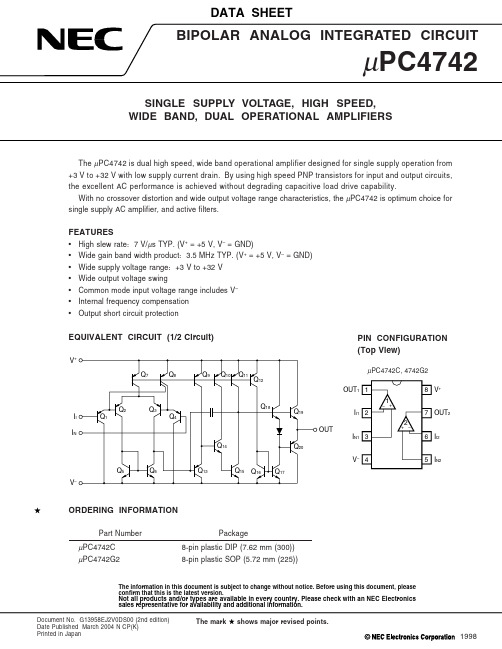
Document No. G13958EJ2V0DS00 (2nd edition) Date Published March 2004 N CP(K)Printed in Japan The mark shows major revised points.1998ABSOLUTE MAXIMUM RATINGS (T A = 25 °C)Parameter Symbol Ratings Unit Voltage between V+ and V– Note 1V+ –V––0.3 to +36V Differential Input Voltage V ID±36V Input Voltage Note 2V I V– –0.3 to V– +36V Output Voltage Note 3V O V– –0.3 to V+ +0.3V Power Dissipation C Package Note 4P T350mWG2 Package Note 5440mW Output Short Circuit Duration Note 6Indefinite sec Operating Ambient Temperature T A–20 to +80°C Storage Temperature T stg–55 to + 125°CNotes1.Reverse connection of supply voltage can cause destruction.2.The input voltage should be allowed to input without damage or destruction independent of themagnitude of V+. Either input signal should not be allowed to go negative by more than 0.3 V. The normaloperation will establish when the both inputs are within the Common Mode Input Voltage Range ofelectrical characteristics.3.This specification is the voltage which should be allowed to supply to the output terminal from externalwithout damage or destructive. Even during the transition period of supply voltage, power on/off etc.,this specification should be kept. The output voltage of normal operation will be the Output Voltage Swingof electrical characteristics.4.Thermal derating factor is –5.0 mW/°C when operating ambient temperature is higher than 55 °C.5.Thermal derating factor is –4.4 mW/°C when operating ambient temperature is higher than 25 °C.6.Pay careful attention to the total power dissipation not to exceed the absolute maximum ratings, Note4 and Note 5.RECOMMENDED OPERATING CONDITIONSParameter Symbol MIN.TYP.MAX.Unit Supply Voltage (Split)V±±1.5±16V Supply Voltage (V– = GND)V++3+32V Output Current I O±10mA Capacitive Load (A V = +1, R f = 0 Ω)C L1000pF2Data Sheet G13958EJ2V0DSELECTRICAL CHARACTERISTICS (T A = 25 °C, V± = ±15 V)Parameter Symbol Conditions MIN.TYP.MAX.UnitInput Offset Voltage V IO±1.0±4.5mV Input Offset Current I IO±6±75nA Input Bias Current Note 7I B140500nA Large Signal Voltage Gain A V R L≥ 2 kΩ, V O = ±10 V25000300000Supply Current Note 8I CC I O = 0 A 4.3 5.5mA Common Mode Rejection Ratio CMR7086dB Supply Voltage Rejection Ratio SVR7093dBOutput Voltage Swing V om R L≥ 10 kΩ±13.7+14V–14.3Output Voltage Swing V om R L≥ 2 kΩ±13.5V Common Mode lnput Voltage Range V ICM V–V+–1.8V Slew Rate (Rise)SR A V = 1, R L≥ 2 kΩ8.5V/µs Gain Band Width Product GBW f O = 100 kHz 3.5MHz Channel Separation f = 20 Hz to 20 kHz120dBELECTRICAL CHARACTERISTICS (T A = 25 °C, V+ = 5 V, V– = GND)Parameter Symbol Conditions MIN.TYP.MAX.Unit Input Offset Voltage V IO±1.0±5mV Input Offset Current I IO±6±75nA Input Bias Current Note 7I B160500nA Large Signal Voltage Gain A V R L≥ 2 kΩ25000300000Supply Current Note 8I CC I O = 0 A 3.3 4.5mA Common Mode Rejection Ratio CMR7080dB Supply Voltage Rejection Ratio SVR7095dBOutput Voltage Swing V om R L≥ 2 kΩ (Connect to GND) 3.7 4.0V00Common Mode lnput Voltage Range V ICM0V+–1.8V Output Current (SOURCE)I O SOURCE V+IN = +1 V, V–IN = 0 V1030mA Output Current (SINK)I O SINK V+IN = 0 V, V–IN = +1 V1030mA Slew Rate (Rise)SR7V/µsNotes7.Input bias currents flow out from IC. Because each currents are base current of PNP-transistor on input stage.8.This current flows irrespective of the existence of use.3Data Sheet G13958EJ2V0DS4Data Sheet G13958EJ2V0DSTYPICAL CHARACTERISTICS (T A = 25 °C, TYP.)POWER DISSIPATIONP T - T o t a l P o w e r D i s s i p a t i o n - m WV I O - I n p u t O f f s e t V o l t a g e - m VSUPPLY CURRENT V + - Supply Voltage - V (V – = GND)543210–1–2–3–4–5I B - I n p u t B i a s C u r r e n t - n AT A - Operating Ambient Temperature - °C5Data Sheet G13958EJ2V0DSA V - O p e n L o o p V o l t a g e G a i n - d BOUTPUT SINK CURRENT LIMITV O - O u t p u t V o l t a g e - VOUTPUT SOURCE CURRENT LIMIT 0123t - Time - sµT A - Operating Ambient Temperature - °CV I N - I n p u t V o l t a g e -V /V O - O u t p u t V o l t a g e - V10050–506Data Sheet G13958EJ2V0DSPACKAGE DRAWINGS (Unit: mm)ITEM MILLIMETERS NOTES1. Each lead centerline is located within 0.25 mm ofits true position (T.P.) at maximum material condition.P8C-100-300B,C-2N 0.25P 0.9 MIN.R0∼15°A 10.16 MAX.B 1.27 MAX.F 1.4 MIN.G 3.2±0.3J 5.08 MAX.K 7.62 (T.P.)C 2.54 (T.P.)D 0.50±0.10H 0.51 MIN.I 4.31 MAX.L 6.4M 0.25+0.10−0.052. ltem "K" to center of leads when formed parallel.8-PIN PLASTIC DIP (7.62mm(300))7Data Sheet G13958EJ2V0DSITEM B C I 8-PIN PLASTIC SOP (5.72 mm (225))D E F G H J PMILLIMETERS 1.27 (T.P.)0.78 MAX.4.4±0.150.1±0.10.421.59±0.216.5±0.31.49+0.08−0.071.1±0.23°+7°−3°NOTEEach lead centerline is located within 0.12 mm ofits true position (T.P.) at maximum material condition.A 5.2+0.17−0.20K L M N 0.6±0.20.170.120.10+0.08−0.07S8GM-50-225B-6RECOMMENDED SOLDERING CONDITIONSThe µPC4742 should be soldered and mounted under the following recommended conditions.For soldering methods and conditions other than those recommended below, contact an NEC Electronics sales representative.For technical information, see the following website.Semiconductor Device Mount Manual (/pkg/en/mount/index.html)Type of Surface Mount DeviceµPC4742G2: 8-pin plastic SOP (225 mil)Process Conditions SymbolInfrared ray reflow Peak temperature: 230 °C or below (Package surface temperature),IR30-00-1Reflow time: 30 seconds or less (at 210 °C or higher),Maximum number of reflow processes: 1 time.Vapor Phase Soldering Peak temperature: 215 °C or below (Package surface temperature),VP15-00-1Reflow time: 40 seconds or less (at 200 °C or higher),Maximum number of reflow processes: 1 time.Wave Soldering Solder temperature: 260 °C or below, Flow time: 10 seconds or less,WS60-00-1Maximum number of flow processes: 1 time,Pre-heating temperature: 120 °C or below (Package surface temperature).Partial heating method Pin temperature: 300 °C or below,–Heat time: 3 seconds or less (Per each side of the device).Caution Apply only one kind of soldering condition to a device, except for “partial heating method”, or the device will be damaged by heat stress.Type of Through-hole DeviceµPC4742C: 8-pin plastic DIP (300 mil)Process ConditionsWave soldering Solder temperature: 260 °C or below,(only to leads)Flow time: 10 seconds or less.Partial heating method Pin temperature: 300 °C or below,Heat time: 3 seconds or less (per each lead).Caution For through-hole device, the wave soldering process must be applied only to leads, and make sure that the package body does not get jet soldered.8Data Sheet G13958EJ2V0DSREFERENCE DOCUMENTSQUALITY GRADES ON NEC SEMICONDUCTOR DEVICES C11531ESEMICONDUCTOR DEVICE MOUNT MANUAL /pkg/en/mount/index.html NEC SEMICONDUCTOR DEVICE RELIABILITY/QUALITY CONTROL SYSTEM IEI-1212(STANDARD LINEAR IC)9Data Sheet G13958EJ2V0DSThe information in this document is current as of March, 2004. The information is subject to change without notice. For actual design-in, refer to the latest publications of NEC Electronics data sheets or data books, etc., for the most up -to-date sp ecifications of NEC Electronics p roducts. Not all p roducts and/or typ es are available in every country. Please check with an NEC Electronics sales representative for availability and additional information.No part of this document may be copied or reproduced in any form or by any means without the prior written consent of NEC Electronics. NEC Electronics assumes no responsibility for any errors that may appear in this document.NEC Electronics does not assume any liability for infringement of patents, copyrights or other intellectual property rights of third parties by or arising from the use of NEC Electronics products listed in this document or any other liability arising from the use of such products. No license, express, implied or otherwise, is granted under any patents, copyrights or other intellectual property rights of NEC Electronics or others.Descriptions of circuits, software and other related information in this document are provided for illustrative purposes in semiconductor product operation and application examples. The incorporation of these circuits, software and information in the design of a customer's equipment shall be done under the full responsibility of the customer. NEC Electronics assumes no responsibility for any losses incurred by customers or third parties arising from the use of these circuits, software and information.While NEC Electronics endeavors to enhance the quality, reliability and safety of NEC Electronics products, customers agree and acknowledge that the possibility of defects thereof cannot be eliminated entirely. To minimize risks of damage to property or inj ury (including death) to persons arising from defects in NEC Electronics products, customers must incorporate sufficient safety measures in their design, such as redundancy, fire-containment and anti-failure features.NEC Electronics products are classified into the following three quality grades: "Standard", "Special" and "Specific".The "Specific" quality grade applies only to NEC Electronics products developed based on a customer-designated "quality assurance program" for a specific application. The recommended applications of an NEC Electronics product depend on its quality grade, as indicated below. Customers must check the quality grade of each NEC Electronics product before using it in a particular application."Standard":Computers, office equipment, communications equipment, test and measurement equipment, audioand visual equipment, home electronic appliances, machine tools, personal electronic equipment and industrial robots."Special":Transportation equipment (automobiles, trains, ships, etc.), traffic control systems, anti-disastersystems, anti-crime systems, safety equipment and medical equipment (not specifically designed for life support)."Specific":Aircraft, aerospace equipment, submersible repeaters, nuclear reactor control systems, lifesupport systems and medical equipment for life support, etc.The quality grade of NEC Electronics products is "Standard" unless otherwise expressly specified in NEC Electronics data sheets or data books, etc. If customers wish to use NEC Electronics products in applications not intended by NEC Electronics, they must contact an NEC Electronics sales representative in advance to determine NEC Electronics' willingness to support a given application.(Note)(1)"NEC Electronics" as used in this statement means NEC Electronics Corporation and also includes itsmajority-owned subsidiaries.(2)"NEC Electronics products" means any product developed or manufactured by or for NEC Electronics (asdefined above).••••••M8E 02. 11-1。
PC929中文资料

g TÜV ( VDE 0884 ) approved type is also available as an option.
s Features 1. Built-in IGBT shortcircuit protector circuit 2. Built-in direct drive circuit for IGBT drive
V
VCC = V01 = 24V, RG = 47Ω
6.5 6.0 5.5
CG = 3 000pF, FS = OPEN
1
2
3
V
(9)
*9
O2 "High→Low" delay time at protection from overcurrent
tPCOHL
Ta = 25˚C
-
4
10
µs
O2 fall time at protection from overcurrent
Amp.
1 2 3 4 5 67
1 Cathode 2 Cathode 3 Anode 4 NC 5 NC 6 NC 7 NC
8 FS
9C
10 GND
11 O2 12 O1 13 VCC 14 GND
Terminals 4 to 7 : Shortcircuit in element
* "OPIC" (Optical IC) is a trademark of the SHARP Corporation. An OPIC consists of a light-detecting element and signal processing circuit integrated onto a single chip.
整流桥型号大全

上海好明电子整流桥型号上海好明电子专业生产整流桥,二极管,三极管,LED,PTC,整流模块等产品整流桥分类为:1、LED迷你整流桥;2、整流桥圆桥;3、整流桥扁桥;4、整流桥方桥。
◆LED迷你整流桥:◇MBS封装:MB1S、MB2S、MB4S、MB6S、MB8S、MB10S◇MBM封装:MB1M、MB2M、MB4M、MB6M、MB8M、MB10M◇DB封装:DB101、DB102、DB103、DB104、DB105、DB106、DB107◇DBS封装:DB101S、DB102S、DB103S、DB104S、DB105S、DB106S、DB107S◆整流桥圆桥:◇WOW封装:W005M、W01M、W02M、W04M、W06M、W08M、W10M◇WOW封装:2W005M、2W01M、2W02M、2W04M、2W06M、2W08M、2W10M◆整流桥扁桥:◇KBP封装:KBP2005、KBP201、KBP202、KBP204、KBP206、KBP208、KBP210◇KBP封装:RS201、RS202、RS203、RS204、RS205、RS206、RS207◇GBP封装:GBP2005、GBP201、GBP202、GBP204、GBP206、GBP208、GBP210◇KBP封装:RS301、RS302、RS303、RS304、RS305、RS306、RS307◇KBL封装:KBL4005、KBL401、KBL402、KBL404、KBL406、KBL408、KBL410◇GBU封装:GBU4005、GBU401、GBU402、GBU404、GBU406、GBU408、GBU410◇KBJ封装:KBJ4005、KBJ401、KBJ402、KBJ404、KBJ406、KBJ408、KBJ410◇GBL封装:GBL4005、GBL401、GBL402、GBL404、GBL406、GBL408、GBL410◇KBU封装:、KBU601、KBU602、KBU604、KBU606、KBU608、KBU610◇GBU封装:GBU6005、GBU601、GBU602、GBU604、GBU606、GBU608、GBU610◇KBJ封装:KBJ6005、KBJ601、KBJ602、KBJ604、KBJ606、KBJ608、KBJ610◇KBU封装:KBU8005、KBU801、KBU802、KBU804、KBU806、KBU808、KBU810◇GBU封装:GBU8005、GBU801、GBU802、GBU804、GBU806、GBU808、GBU810◇KBJ封装:KBJ8005、KBJ801、KBJ802、KBJ804、KBJ806、KBJ808、KBJ810◇KBU封装:KBU10005、KBU1001、KBU1002、KBU1004、KBU1006、KBU1008、KBU1010◇GBU封装:GBU10005、GBU1001、GBU1002、GBU1004、GBU1006、GBU1008、GBU1010◇KBJ封装:KBJ10005、KBJ1001、KBJ1002、KBJ1004、KBJ1006、KBJ1008、KBJ1010◇GBJ封装:GBJ15005、GBJ1501、GBJ1502、GBJ1504、GBJ1506、GBJ1508、GBJ1510◇GBJ封装:GBJ25005、、GBJ2502、GBJ2504、GBJ2506、GBJ2508、GBJ2510◆整流桥方桥:◇KBPC3封装:KBPC3005、KBPC301、KBPC302、KBPC304、KBPC306、KBPC308、KBPC310◇KBPC6封装:KBPC6005、KBPC601、KBPC602、KBPC604、KBPC606、KBPC608、KBPC610◇KBPC8封装:KBPC8005、KBPC801、KBPC802、KBPC804、KBPC806、KBPC808、KBPC810◇KBPC8封装:KBPC10005、KBPC1001、KBPC1002、KBPC1004、KBPC1006、KBPC1008、KBPC1010、◇MB-35封装:KBPC15005、KBPC1501、KBPC1504、KBPC1506、KBPC1508、KBPC1510◇MB-35W封装:KBPC15005W、KBPC1501W、KBPC1504W、KBPC1506W、KBPC1508W、KBPC1510W◇GBPC35封装:GBPC15005、GBPC1501、GBPC1502、GBPC1504、GBPC1506、GBPC1508、GBPC1510◇GBPC35W封装:GBPC15005W、GBPC1501W、GBPC1502W、GBPC1504W、GBPC1506W、GBPC1508W、GBPC1510W ◇MB-35封装:KBPC25005、KBPC2501、KBPC2502、KBPC2504、KBPC2506、KBPC2508、KBPC2510◇MB-35W封装:KBPC25005W、KBPC2501W、KBPC2502W、KBPC2504W、KBPC2506W、KBPC2508W、KBPC2510W ◇GBPC35封装:GBPC25005、GBPC2501、GBPC2502、GBPC2504、GBPC2506、GBPC2508、GBPC2510◇GBPC35W封装:GBPC25005W、GBPC2501W、GBPC2502W、GBPC2504W、GBPC2506W、GBPC2508W、GBPC2510W ◇MB-35封装:KBPC35005、KBPC3501、KBPC3502、KBPC3504、KBPC3506、KBPC3508、KBPC3510◇MB-35W封装:KBPC35005W、KBPC3501W、KBPC3502W、KBPC3504W、KBPC3506W、KBPC3508W、KBPC3510W ◇GBPC35封装:GBPC35005、GBPC3510、GBPC3502、GBPC3504、GBPC3506、GBPC3508、GBPC3510◇GBPC35W封装:GBPC35005W、GBPC3510W、GBPC3502W、GBPC3504W、GBPC3506W、GBPC3508W、GBPC3510W ◇MB-35封装:KBPC40005、KBPC4001、KBPC4002、KBPC4004、KBPC4006、KBPC4008、KBPC4010◇GBPC35封装:GBPC40005、GBPC4001、GBPC4002、GBPC4004、GBPC4006、GBPC4008、GBPC4010◇MB-35封装:KBPC50005、KBPC5001、KBPC5002、KBPC5004、KBPC5006、KBPC5008、KBPC5010◇MB-35W封装:KBPC50005W、KBPC5001W、KBPC5002W、KBPC5004W、KBPC5006W、KBPC5008W、KBPC5010W ◇GBPC35封装:GBPC50005、GBPC5001、GBPC5002、GBPC5004、GBPC5006、GBPC5008、GBPC5010◇GBPC35W封装:GBPC50005W、GBPC5001W、GBPC5002W、GBPC5004W、GBPC5006W、GBPC5008W、GBPC5010W。
RC4558中文详细资料
电气特性:
参数
符号
测试条件
最小
典型
最大
单位
电源电流,所有的放大器,无负载
Icc
2.3
4.5
mA
Input offset voltage输入失调电压
VIO
Rs<10KΩ
2
6
mV
Input offset current输入失调电流
IIO
5
200
nA
Input bias current输入偏置电流
IBIAS
参数符号测试条件最小典型最大单位电源电流所有的放大器无负载icc2345mainputoffsetvoltage输入失调电压viors10k?mvinputoffsetcurrent输入失调电流iio200nainputbiascurrent输入偏置电流ibias30500nalargesignalvoltagegain大信号电压增益gvvopp10vrl2k?20200vmvcommonmodeinputvoltagerange输入电压范围vir1213commonmoderejectionratio共模抑制cmrrrs10k?7090dbsupplyvoltagerejectionratio电源电压抑制比psrrrs10k?7690dboutputvoltageswing输出电压摆幅vopprl10k?1214powerconsumption功耗pc70170mvslewratesrvi10vrl2kcl100pf1222risetime上升时间trisvi20mvrl2kcl100pf03overshoot上过冲osvi20mvrl2kcl100pf15inputresistance输入电阻ri03outputresistance输出电阻ro75totalharmonicdistortion总谐波失真thdf1khzav20dbrl2kvo2vppcl100pf0008单位增益带宽bw28mhz