SY89311UMG TR;SY89311UMI TR;中文规格书,Datasheet资料
GSI TympStar 产品说明书

P.O. BOX 44994 •MADISON WI 53744.4994 •PHONE: +1.608.441.2323 •TOLL FREE: 800.700.2282GRASON-STADLER NICOLET BIOMEDICAL NICOLET VASCULAR TOENNIESPRODUCT SPECIFICATIONS November 2004 | GSI TympStar | 2000-0112 Rev1The following specifications apply to both Version 1and Version 2 of the GSI TympStar. > Bold arrowed type indicates the additional capabilities of Version 2.GENERAL SPECIFICATIONS W x D x H: 52 cm x 38 cm x 32 cm Weight: 7.5 Kg Shipping Weight: 13.4 Kg Power Consumption: 120 Watts maximum Test Types: Tympanometry, Acoustic Reflex Threshold,Reflex Decay, Eustachian T ube Function (Intact & Perforated )Protocols: Diagnostic, Screening, User-defined > Special Tests: Two-component T ympanometry,Multiple Frequency T ympanometry, Acoustic Reflex Latency Test, Reflex Sensitization Display: Internal or External VGA Monitor Interface: RS232, parallel and keyboard output Printout: Internal or External Deskjet or Laserjet Printer PROBE TONE 226 Hz (85 dB SPL ±1.5 dB)> 678 Hz (85 dB SPL ±3.0 dB)> 1000 Hz (75 dB SPL ±3.0 dB)Accuracy: ±1%Harmonic Distortion: Less than 5%ADMITTANCE MEASUREMENTS Range: 226 Hz (-1.0 to +7.0)> 678 Hz (-5.0 to +25)> 1000 Hz (-5.0 to +30)Sensitivity Scale: Auto Scales to Appropriate Range,Manual selection also possible in Reflex Modes only Accuracy (226 Hz): Tymp Mode: ±5% of reading or ±0.1 ml, whichever is greater Reflex Mode: ±5% of reading or ±0.2 ml, whichever is greater PRESSURE MEASUREMENTS (load volume of 0.2 to 7.0 ml)Range:Normal = +200 to -400 daPa Wide = +400 to -600 daPa Accuracy: ±10% of reading or ±10 daPa, whichever is greater Sweep Rate: 12.5, 50.0 and 600/200 daPa/sec, > 200 daPa/sec.Sweep Accuracy: 10% of nominal rate Maximum limits (in 0.5cc cavity ): -800 daPa & +600 daPa REFLEX MEASUREMENTS Stimuli: > 250, 500, 1k, 2k, 4k, BBN, LBN, HBN,> Click (100 microseconds pulse), External Input,Non-acoustic Frequency Accuracy: ±3%Harmonic Distortion (THD): Less than 5% (measured acoustically)Noise Signals: (3 dB bandwidths)Low Band: 125 -1,600 Hz High Band: 1,600 -4,000 Hz Broad Band: 125 -4,000 Hz Intensity Range: 35 to 120 dB HLStep Size: 5 dB, >1 dB and 2 dB Calibration Accuracy: ±3 dB Step Accuracy: ±0.5 dB ON/OFF Ratio: 70 dB minimum ENVIRONMENTAL Temperature:Storage: -40°C to +75°C Operating: +15°C to +35°C Humidity: 90% at 35°C (non-condensing)ACCESSORIES SUPPLIED Probe assembly (including contralateral insert phone)Eartips (1 pkg. each standard, special, screening)Printer paper, 2 rolls thermal, 1 roll self-adhesive Calibration test cavity, Cleaning kit, Probe mount kit (shoulder, clip, wrist band), Quick User Guide,Reference Instruction Manual, Remote (RS232 link)Dust CoverOPTIONAL ACCESSORIES Deskjet printer 1700-9613External VGA monitor 1700-9614External keyboard 1700-9615Isolation Transformer 1700-9617Service Manual 2000-0110Conversion Kit 2000-9650(V1 to V2)LANGUAGE KITS GSI TympStar Version 1English 2000-9645E French 2000-9645F German 2000-9645G Spanish 2000-9645S Italian 2000-9645I GSI TympStar Version 2English 2000-9646E French 2000-9646F German 2000-9646G Spanish 2000-9646S Italian 2000-9646I QUALITY SYSTEM Manufactured, designed, developed and marketed by VIASYS Healthcare Inc. NeuroCare Group under ISO 13485, ISO 9001 certified quality system.COMPLIANCE / REGULATORY STANDARDSDesigned, tested and manufactured to meet the following domestic (USA), Canadian, European and International Standards:UL 2601-1American Standards for Medical Electrical Equipment. IEC 601-1, EN 60601-1International Standards for Medical Electrical Equipment.CSA C22.2 # 601-1-M90Medical Device Directive (MDD) (ID No.: 0344) to comply with “EC Directive” 93/42/EECANSI S3.39, ANSI S3.6, IEC 645-1, IEC 1027, ISO 389GSI TYMPSTAR ™Middle Ear Analyzer。
AG9311规格说明书
AG9311USB Type-C to HDMI with Power Delivery 3.0ConverterData SheetOfficial VersionV1.6July, 2018Revision HistoryIndexI. General Description (5)II. Features (5)III. Device Information (6)IV. Application (6)V. System Block Diagram (7)VI. Pin Mapping and Description (8)VII. Specification (15)i. Absolute Maximum Rating (15)ii. DC Characteristics/Operating Conditions (15)iii. AC Characteristics (16)VIII. Packing and Marking Specification (19)IX. References (22)X. (22)List of FigureFigure 1 Application for Type-C to HDMI Dongle (6)Figure 2 System Block Diagram (7)Figure 3 AG9311-MAQ Pin Mapping (8)Figure 4 AG9311-MCQ Pin Mapping (12)Figure 5 AG9311-MAQ Package Dimension (20)Figure 6 AG9311-MCQ Package Dimension (21)List of TableTable 1 PIN Description (9)Table 2 PIN Description (12)Table 3 Absolute Maximum Rating (15)Table 4 Digital I/O Specification (16)Table 5 DisplayPort Input Timing (16)Table 6 DisplayPort AUX Channel I/O Specification (17)Table 7 USB I/O Specification (18)Table 8 USB PD Specification (18)I.General DescriptionALGOL TEK AG9311 is highly integration solution transmit video and audio stream from DP alternate mode over USB Type-C to HDMI output. The AG9311 provides DisplayPort 1.2 receiver over various @1.62Gbps, 2.7Gbps and 5.4Gbps up to 2 lanes; and supports HDMI frequencies up to 297MHz, which enables 4K x 2K@30Hz. User easily integrate AG9311 on any USB Type-C video conversion on dongles and docking stations application.II.Features●DisplayPort-Compliant to DisplayPort specification Revision 1.2-Support 1.62(RBR)/2.7(HBR)/5.4(HBR2) Gbps data rate-Support 1/2 Lane configurations-Down Spread Spectrum Clock (SSC) supported-Support Audio Extraction over I2S bus●HDMI-Compliant to HDMI1.4 and HDCP1.4 specifications-Support TMDS up to 3Gbps-Support resolution up to 4K x 2K @30Hz output-Pre-programmed with HDCP key-Transparent EDID and MCCS-Support LPCM 2-Channel of sample rate 48kHz/44.1KHz/32KHz●USB Type-C and Power Delivery-Support DisplayPort Alternate mode protocol-Compliant to USB Power Delivery specification Revision 3.0-Integrated complete termination of the Type-C R P and R D resistors-Supports two USB Type-C port-Support USB Billboard function-Integrated USB2.0 Full-speed PHY●MCU System and Interface-Embedded 16 bit MCU on-chip-Embedded 64KB flash for firmware upgrade-Support I2C Master/Slave, UART and USB2.0 Full-speed-Support 3-Channel ADC-8bit resolutions●Power Operation and ESD-3.3V: 3V to 3.6V operation-1.2V: 1.08 to 1.32V operation-1.2V Core power and 3.3V I/O power-HBM 2KV ESD performanceAG9311Figure 1 Application for Type-C to HDMI DongleV.System Block DiagramVI.Pin Mapping and DescriptionFigure 3 AG9311-MAQ Pin MappingTable PIN DescriptionVII.Specificationi.Absolute Maximum RatingTable 4 Digital I/O Specification iii.AC CharacteristicsTable 5 DisplayPort Input TimingVIII.Packing and Marking Specification MarkingAGX1X2X3X4 - X5X6L4L5L6L7L8L9L10L112P3P4P5P6P7P8PPackage DimensionAG9311-MAQ: QFN-64L 8x8mm(E-PAD SIZE:181x18*MIL)Figure 5 AG9311-MAQ Package DimensionAG9311-MCQ: QFN-48L 6x6mm(E-PAD SIZE:185x18*MIL)Figure 6 AG9311-MCQ Package DimensionIX.References●DisplayPort TM Standard 1.2b Specification●HDMI 1.4b SpecificationX.Contact InformationTrademark AcknowledgementsThe company and product names mentioned in this document may be the trademarks or registered trademarks of their manufactures.DisclaimerAlgoltek, Inc. reserves the right to change this product without prior notice.Algoltek, Inc. makes no warranty for the use of its products and bears no responsibility for any error that appear in this document. Specifications are subject to change without prior notice.。
半导体传感器ADG1408YRUZ中文规格书
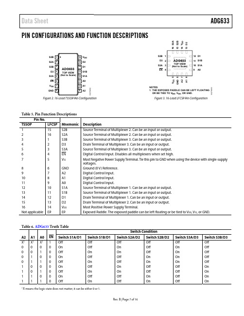
Data SheetADG633Rev. B | Page 7 of 16 PIN CONFIGURATIONS AND FUNCTION DESCRIPTIONSS2A S3B D3V SS EN S3A S2B GND D2D1S1B A1A2A0S1A V DD 03275-002Figure 2. 16-Lead TSSOP Pin Configuration NOTES 1.THE EXPOSED PADDLE CAN BE LEFT FLOATING OR BE TIED TO V DD , V SS , OR GND.S3B D3S3A EN S1B D1S1A A0V S S G N D A 2A 1S 2B S 2A V D DD 203275-00312111013492657816151413ADG633TOP VIEW (Not to Scale)Figure 3. 16-Lead LFCSP Pin Configuration1 X means the logic state does not matter; it can be either 0 or 1.ADG633Data SheetRev. B | Page 14 of 16OUTLINE DIMENSIONSCOPLANARITY 0.10COMPLIANT TO JEDEC STANDARDS MO-153-AB Figure 31. 16-Lead Thin Shrink Small Outline Package [TSSOP] (RU-16) Dimensions shown in millimeters4.104.00 SQ 3.900.350.300.25 2.252.10 SQ1.9510.65BSC BOTTOM VIEW TOP VIEW 16589121340.700.600.50SEATING PLANE0.05 MAX 0.02 NOM 0.203 REF 0.25 MINCOPLANARITY 0.08PIN 1INDICATOR 0.800.750.70COMPLIANT TO JEDEC STANDARDS MO-220-WGGC.FOR PROPER CONNECTION OF THE EXPOSED PAD, REFER TO THE PIN CONFIGURATION AND FUNCTION DESCRIPTIONS SECTION OF THIS DATA SHEET.04-15-2016-A P K G -004025/5112PIN 1INDIC ATOR AREA OPTIONS (SEE DETAIL A)DETAIL A (JEDEC 95)EXPOSED PAD Figure 32. 16-Lead Frame Chip Scale Package [LFCSP] 4 mm × 4 mm Body and 0.75 mm Package Height (CP-16-23) Dimensions shown in millimetersORDERING GUIDEModel 1Temperature Range Package Description Package Option ADG633YRU−40°C to +125°C 16-Lead Thin Shrink Small Outline Package [TSSOP] RU-16 ADG633YRU-REEL7−40°C to +125°C 16-Lead Thin Shrink Small Outline Package [TSSOP] RU-16 ADG633YRUZ−40°C to +125°C 16-Lead Thin Shrink Small Outline Package [TSSOP] RU-16 ADG633YRUZ-REEL7−40°C to +125°C 16-Lead Thin Shrink Small Outline Package [TSSOP] RU-16 ADG633YCPZ−40°C to +85°C 16-Lead Lead Frame Chip Scale Package [LFCSP] CP-16-23 ADG633YCPZ-REEL7−40°C to +85°C 16-Lead Lead Frame Chip Scale Package [LFCSP] CP-16-23 1 Z = RoHS Compliant Part.。
SY89297UMH;SY89297UMG;SY89297UMG TR;SY89297UMH TR;中文规格书,Datasheet资料
SY89297U2.5/3.3V, 3.2Gbps Precision CML Dual-Channel Programmable DelayPrecision Edge is a registered trademark of Micrel, Inc.Micrel Inc. • 2180 Fortune Drive • San Jose, CA 95131 • USA • tel +1 (408) 944-0800 • fax + 1 (408) 474-1000 •General DescriptionThe SY89297U is a DC-3.2Gbps programmable, two-channel delay line. Each channel has a delay range from 2ns to 7ns (5ns delta delay) in programmable increments as small as 5ps. The delay step is extremely linear and monotonic over the entire programming range, with 15ps INL over temperature and voltage.The delay varies in discrete steps based on a serial control word provided by the 3-pin serial control (SDATA, SCLK, and SLOAD). The control word for each channel is 10-bits. Both channels are programmed through a common serial interface. For increased delay, multiple SY89297U delay lines can be cascaded together.The SY89297U provides two independent 3.2Gbps delay lines in an ultra-small 4mm x 4mm, 24-pin QFN package. For other delay line solutions, consider the SY89295U and SY89296U single-channel delay lines. Evaluation boards are available for all these parts.Datasheets and support documentation can be found on Micrel’s web site at: .Precision Edge ®Features• Dual-channel, programmable delay line• Serial programming interface (SDATA, SCLK, SLOAD) • Guaranteed AC performance over temperature and voltage:– > 3.2Gbps/1.6GHz f MAX • Programming Accuracy: – Linearity: −15ps to +15ps INL – Monotonic: −5ps to +25ps– Resolution: 5ps programming increments • Low-jitter design: 1ps RMS typical random jitter • Programmable delay range: 5ns delay range • Cascade capability for increased delay • Flexible voltage operation:– V CC = 2.5V ± 5% or 3.3V ± 10% • Industrial temperature range: −40°C to +85°C • Available in 24-pin (4mm x 4mm) QFNApplications• Clock de-skewing • Timing adjustments • Aperture centering • System calibrationMarkets• Automated test equipment• Digital radio and video broadcasting • Closed caption encoders/decoders • Test and measurementOrdering Information(1)Part Number Package Type Operating Range Package Marking Lead FinishSY89297UMG QFN-24 Industrial 297U with Pb-Free Bar Line Indicator Pb-Free NiPdAuSY89297UMGTR(2)QFN-24 Industrial 297U with Pb-Free Bar-Line Indicator Pb-Free NiPdAuNotes:1. Contact factory for die availability. Dice are guaranteed at T= 25°C, DC electricals only.A2. Tape and Reel.Pin Configuration24-Pin QFNTruth TablesInputs Outputs INA, INB /INA, /INB QA, QB /QA, /QB0 1 0 11 0 1 0Table 1. Inputs/Outputs/ENA, /ENB Q, /Q (A, B)1 Q = Low, /Q = HIGH0 IN, /IN Delayed (normal operation)Table 2. Input Enable (Latches Outputs)Functional Block DiagramPin DescriptionPin NumberPin Name Pin Function1 2INA /INAChannel A Differential Input: INA and /INA pins receive the Channel A data. QA and /QA are the delayed product of INA and /INA. Each input is internally terminated to VTA through a 50Ω resistor (100Ω across INA and /INA).3 VTA Input A Termination Center-Tap: Each side of the differential input pair terminates to this pin.This pin provides a center-tap to a termination network for maximum interface flexibility. See“Input Interface Applications” section. 4 VTBInput B Termination Center-Tap: Each side of the differential input pair terminates to this pin. This pin provides a center-tap to a termination network for maximum interface flexibility. See “Input Interface Applications” section. 5 6INB /INBChannel B Differential Input: INB and /INB pins receive the Channel B data. QB and /QB are the delayed product of INB and /INB. Each input is internally terminated to VTB through a 50Ω resistor (100Ω across INB and /INB).7 VREF-ACReference Voltage Output: For AC-coupled input signals, this pin can bias the inputs IN and /IN. Connect VREF-AC directly to the VT input pin for each channel. De-couple to V CC using a0.01µF capacitor. Maximum sink/source current is ±0.5mA. For DC-coupled input applications, leave VREF-AC pin floating. 8, 11, 20GND, Exposed PadNegative Supply: Exposed pad must be connected to a ground plane that is the same potential as the ground pins.9 /ENACMOS/TTL-Compatible Enable Input: When the /ENA pin is pulled HIGH, QA is held LOW and /QA goes HIGH after the programmed delay propagates through the part. /ENA contains a 67k Ω pull-down resistor and defaults LOW when left floating. Logic threshold level is V CC /2 10 /ENBCMOS/TTL-Compatible Enable Input: When the /ENB pin is pulled HIGH, QB is held LOW and /QB goes HIGH after the programmed delay propagates through the part. /ENB contains a 67k Ω pull-down resistor and defaults LOW when left floating. Logic threshold level is Vcc/2 12, 15, 16, 19VCC Power Supply: Bypass each supply pin with 0.1µF//0.01µF low-ESR capacitors. See DC Electrical Characteristics table for more details. 2.5V ±5% or 3.3V ±10%.13 14 /QB QB CML Differential Output: QB and /QB are the delayed product of INB, /INB. CML outputs are terminated at the destination with 100Ω across the pair. See “CML Output Termination” section.17 18/QA QACML Differential Output: QA and /QA are the delayed product of INA, /INA. CML outputs are terminated at the destination with 100Ω across the pair. See “CML Output Termination” section.23 22SCLK SDATACMOS/TTL-compatible 3-pin serial programming control inputs: The 3-pin serial control sets each channel’s IN to Q delay. DA(0:9) control channel A delay. DB(0:9) control channel B. To program the two channels, insert a 20-bit word (DA0:DA9 and DB0:DB9) into SDATA and clock in the control bits with SCLK. Maximum input frequency to SCLK is 40MHz. Data is loaded into the serial registers on the L-H transition of SCLK. After all 20-bits are clocked in, SLOAD latches the new delay bits. These pins have internal pull-downs at the inputs. See “ACElectrical Characteristics” for delay values. Logic threshold level is Vcc/2. SCLK and SDATA contain a 67k Ω pull-down resistor and default LOW when left floating.24 SLOADCMOS/TTL-compatible 3-pin serial programming control input: SLOAD controls the latches that transfer scanned data to the delay line. These latches are transparent when SLOAD is high. Data transfers from the latch to the delay line on a L-H transition of SLOAD. SLOAD has to transition H-L before new data is loaded in the scan chain. When SLOAD is high, the latches are transparent and SCLK cannot switch. Otherwise, new data will immediately transfer to the scan chain. Logic threshold level is Vcc/2. SLOAD contains a 67k Ω pull-down resistor and defaults LOW when left floating. 21 SOUTCMOS/TTL-compatible output: This pin is used to support cascading multiple SY89297U delay lines. Serial data is clocked into the SDATA input and is clocked out of SOUT into the next SY89297U delay line. SOUT pin includes an internal 550Ω pull-up resistor.Absolute Maximum Ratings(1)Supply Voltage (V CC) .................................. –0.5V to +4.0V Input Voltage (V IN) .......................................... –0.5V to V CC CML Output Voltage (V OUT)… ....... V CC −1.0V to V CC +0.5V Current (V T)Source or Sink Current on VT pin ..................... ±70mA Input CurrentSource or Sink Current on (IN, /IN) .................. ±35mA Current (V REF)Source or sink current on V REF-AC(2) ................ .±0.5mA Maximum operating Junction Temperature ............ 125°C Lead Temperature (soldering, 20sec.) ..................... 260°C Storage Temperature (T s) ....................... –65°C to +150°C Operating Ratings(3)Supply Voltage (V CC)T A (−40°C to +85°C) ................ +2.375V to +2.625VT A (−40°C to +75°C) .......................... +3.0V to 3.6V Ambient Temperature (T A) .......................... −40°C to +85°C Package Thermal Resistance(4)QFN (θJA)Still-Air...............................................................43°C/W QFN (ψJB)Junction-to-Board...........................................30.5°C/WDC Electrical Characteristics(5)T A = −40°C to +85°C, Channels A and B, unless otherwise stated.Symbol Parameter Condition Min. Typ. Max. UnitsV CC Power Supply Voltage Range T A: −40°C to +85°C 2.375 2.5 2.625 V T A: −40°C to +75°C 3.0 3.3 3.6 V T A: −40°C to +85°C,Airflow = 500 LFPM3.0 3.3 3.6 VI CC PowerSupplyCurrent Maximum V CC, Both ChannelsCombined, Output Load Included195 250 mAR IN Input Resistance(IN-to-VT, /IN-to-VT)455055ΩR DIFF_IN Differential Input Resistance(IN-to-/IN)90100110ΩV IH Input HIGH Voltage (IN, /IN) 1.2 V CC V V IL Input LOW Voltage (IN, /IN) 0 V IH–0.1 V V IN Input Voltage Swing (IN, /IN) See Figure 5a 0.1 1.0 VV DIFF_IN Differential Input Voltage Swing(|IN - /IN|)See Figure 5b 0.2 VV REF-AC Output Reference Voltage V CC–1.3 V CC–1.2 V CC–1.1 VV T_IN Voltage from Input to V T 1.28 V Notes:1. Permanent device damage may occur if “Absolute Maximum Ratings” are exceeded. This is a stress rating only and functional operation is notimplied at conditions other than those detailed in the operational sections of this data sheet. Exposure to “Absolute Maximum Rating” conditions for extendedperiodsmayaffectdevicereliability.2. Due to the limited drive capability, use for input of the same package only.3. The data sheet limits are not guaranteed if the device is operated beyond the operating ratings.4. Thermal performance on QFN packages assumes exposed pad is soldered (or equivalent) to the device most negative potential (GND).5. The circuit is designed to meet the DC specifications shown in the table after thermal equilibrium has been established.CML Outputs DC Electrical Characteristics (6)V CC = +2.5V +5% or +3.3V ±10%, R L = 100Ω across the outputs; T A = −40°C to +85°C, unless otherwise stated. Symbol Parameter Condition Min. Typ. Max. Units V OH Output HIGH Voltage R L = 50Ω to V CC V CC −0.020 V CC −0.010V CC VV OUT Output Voltage SwingSee Figure 5a 325 400 mV V DIFF_OUTDifferential Output Voltage SwingSee Figure 5b650 800 mV R OUT Output Source Impedance455055ΩLVTTL/CMOS DC Electrical Characteristics (6)V CC = +2.5V +5% or 3.3V ±10%, T A = −40°C to +85°C, unless otherwise stated. Symbol Parameter Condition Min. Typ. Max. Units V IH Input HIGH Voltage 2.0 V V IL Input LOW Voltage0.8 V I IH Input HIGH Current V IH = VCC 150 µA I IL Input LOW Current V IL = 0.8V50µAV OLOutput LOW Voltage SOUT Pin; I OL =1mA 0.55 VOutput High Leakage CurrentSOUT = V CC 100 µANote:6. The circuit is designed to meet the DC specifications shown in the above table after thermal equilibrium has been established.AC Electrical Characteristics (7)T A = −40°C to +85°C, Channels A and B, unless otherwise stated. Symbol Parameter ConditionMin. Typ. Max. Units f MAXMaximum Operating FrequencyClock: V out Swing >200mV pk 1.6 GHzNRZ Data3.2Gbpst pdPropagation Delay IN to Q; D[0–9]=0 IN to Q; D[0–9]=1023/EN to Q: D[0–9]=0; V TH = V CC /2 SDATA to SOUT (D0–D9=Low), No load1000 5500 1000 20002000 7500 2500 4500pst RANGE Programmable Ranget pd (max) – t pd (min)4150 5115 pst SKEWDuty Cycle Skew t PHL – t PLH Note 84555%AC Electrical Characteristics(7)T A = −40°C to +85°C, Channels A and B, unless otherwise stated.Symbol Parameter Condition Min. Typ. Max. UnitsΔt Step DelayD0 HighD1 HighD2 HighD3 HighD4 HighD5 HighD6 HighD7 HighD8 HighD9 HighD0-D9 High510204080160320640128025605115ps Monotonic −5 25INL IntegralNon-Linearity Note 9 −15 +15 pst S Setup TimeSDATA to SCLKSCLK to SLOAD/EN to INNote 10Note 11400400300pst H Hold TimeSLOAD to SCLKIN to /ENSCLK to SDATANote 12Note 13300−100200pst PW Pulse Width SLOAD 1000 ps t R Release Time /EN to IN Note 14 800 pst JITTER Cycle-to-Cycle JitterTotal JitterRandom JitterNote 15Note 16Note 172202ps RMSps PPps RMSt r, t f Output Rise/Fall Time 20% to 80% (Q) 30 55 80 ps Duty Cycle Input Frequency = 1.6GHz 45 55 % Notes:7. High frequency AC electricals are guaranteed by design and characterization.8. Duty cycle skew guaranteed only for differential operation measured from the cross point of the input to the crosspoint of the output.9. INL (Integral Non-Linearity) is defined from its corresponding point on the ideal delay versus D[9:0] curve as the deviation from its ideal delay. Themaximum difference is the INL. Theoretical Ideal Linearity (TIL) = (measured maximum delay – measured minimum delay) ÷ 1023. INL = measured delay – (measured minimum delay + (step number x TIL)).10. SCLK has to transition L-H a setup time before the SLOAD H-L transition to ensure the valid data is properly latched. See timing diagram "Setupand Hold Time: SCLK and SLOAD.”11. This setup time is the minimum time that /EN must be asserted prior to the next transition of IN / /IN to prevent an output response greater than±75 mV to that IN or /IN transition. See timing diagram Setup, Hold and Release Time: IN and /EN."12. SCLK has to transition L-H a hold time after the SLOAD H-L transition to ensure that the valid data is properly latched before starting to load newdata. See timing diagram "Setup and Hold Time: SCLK and SLOAD.”13. This hold time is the minimum time that /EN must remain asserted after a negative going transition of IN to prevent an output response greater than+75mv to the IN transition. See timing diagram “Setup, Hold, and Release Time: IN and /EN.”14. This release time is the minimum time that /EN must be de-asserted prior to the next IN / /IN transition to affect the propagation delay of IN to Qless than 1ps. See timing diagram “Setup, Hold, and Release Time: IN and /EN.”15. Cycle-to-cycle jitter definition: The variation of periods between adjacent cycles over a random sample of adjacent cycle pairs.T jitter_cc = T n – T n+1, where T is the time between rising edges of the output signal.16. Total jitter definition: With an ideal clock input, no more than one output edge in 1012 output edges will deviate by more than the specified peak-to-peak jitter value.17. Random jitter definition: Jitter that is characterized by a Gaussian distribution, unbounded and is quantified by its standard deviation and mean.Random jitter is measured with a K28.7 comma defect pattern, measured at 1.5Gbps.Timing DiagramsFigure 1. Setup and Hold Time: SDATA and SCLKFigure 2. Setup and Hold Time: SCLK and SLOADTiming Diagrams (Continued)Figure 3. Set-Up, Hold, and Release Time: IN and /ENFigure 4. SLOAD Pulse Width (TPW)Typical Operating CharacteristicsV CC = +2.5V, GND = 0V, V IN = 100mV, R L = 100Ω across the outputs, T A = 25°C.Phase Noise ChartV CC = +2.5V, GND = 0V, V IN = 100mV, R L = 100Ω across the outputs, T A = 25°C.f C: 1GHz Delay Setting: 00001 00110 (2ns)分销商库存信息:MICRELSY89297UMH SY89297UMG SY89297UMG TR SY89297UMH TR。
SY58017UMGTR资料

Micrel, Inc.
ULTRA-PRECISION DIFFERENTIAL CML 2:1 MUX with INTERNAL I/O TERMINATION
Precision Edge SY58017U
Precision Edge® SY58017U ®
PIN DESCRIPTION
Pin Number 1, 2 3, 4 Pin Name IN0, /IN0 IN1, /IN1 Pin Function Differential Input: These input pairs are the differential signal inputs to the device. They accept differential AC- or DC-coupled signals as small as 100mV. Each pin of a pair internally terminates to a VT pin through 50Ω. Note that these inputs will default to an indeterminate state if left open. Please refer to the “Input Interface Applications” section for more details. Input Termination Center-Tap: Each side of the differential input pair terminates to a VT pin. The VT0 and VT1 pins provide a center-tap to a termination network for maximum interface flexibility. See “Input Interface Applications” section for more details. This single-ended TTL/CMOS compatible input selects the inputs to the multiplexer. Note that this input is internally connected to a 25kΩ pull-up resistor and will default to a logic HIGH state if left open. No connect. Positive Power Supply: Bypass with 0.1µF0.01µF low ESR capacitors. 0.01µF capacitor should be as close to VCC pin as possible. Differential Outputs: This CML output pair is the output of the device. Normally terminate with 100Ω across Q and /Q. See “Output Interface Applications” section. It is a logic function of the IN0, IN1, and SEL inputs. Please refer to the “Truth Table” for details. Ground. Ground pins and exposed pad must be connected to the same ground plane.
半导体传感器ADUM3210TRZ中文规格书

ADuM1400/ADuM1401/ADuM1402Data Sheet Rev. L | Page 14 of 31Parameter Symbol MinTyp Max Unit Test Conditions ADuM1400WTRWZ /ADuM1401WTRWZ / ADuM1402WTRWZMinimum Pulse Width 3 PW100 ns C L = 15 pF, CMOS signal levels Maximum Data Rate 4 10Mbps C L = 15 pF, CMOS signal levels Propagation Delay 5 t PHL , t PLH 2034 45 ns C L = 15 pF, CMOS signal levels Pulse Width Distortion, |t PLH − t PHL |5 PWD3 ns C L = 15 pF, CMOS signal levels Change vs. Temperature5 ps/°C C L = 15 pF, CMOS signal levels Propagation Delay Skew6 t PSK22 ns C L = 15 pF, CMOS signal levels Channel-to-Channel Matching, Codirectional Channels 7 t PSKCD3 ns C L = 15 pF, CMOS signal levels Channel-to-Channel Matching, Opposing-Directional Channels 7 t PSKOD6 ns C L = 15 pF, CMOS signal levels For All ModelsOutput Disable Propagation Delay (High/Low to High Impedance) t PHZ , t PLH6 8 ns C L = 15 pF, CMOS signal levels Output Enable Propagation Delay (High Impedance to High/Low) t PZH , t PZL6 8 ns C L = 15 pF, CMOS signal levels Output Rise/Fall Time (10% to 90%) t R /t F3 ns C L = 15 pF, CMOS signal levels Common-Mode Transient Immunity at Logic High Output 8 |CM H | 2535 kV/µs V Ix = V DD1/V DD2, V CM = 1000 V, transient magnitude = 800 V Common-Mode Transient Immunity at Logic Low Output 8 |CM L | 2535 kV/µs V Ix = 0 V, V CM = 1000 V, transient magnitude = 800 V Refresh Rate f r1.1 Mbps Input Dynamic Supply Current per Channel 9 I DDI (D)0.10 mA/Mbps Output Dynamic Supply Current perChannel 9I DDO (D) 0.03 mA/Mbps 1All voltages are relative to their respective ground. 2 The supply current values for all four channels are combined when running at identical data rates. Output supply current values are specified with no output load present. The supply current associated with an individual channel operating at a given data rate may be calculated as described in the Power Consumption section. See Figure 8 through Figure 10 for information on per-channel supply current as a function of data rate for unloaded and loaded conditions. See Figure 11 through Figure 15 for total V DD1 and V DD2 supply currents as a function of data rate for ADuM1400W /ADuM1401W /ADuM1402W channel configurations. 3 The minimum pulse width is the shortest pulse width at which the specified pulse width distortion is guaranteed. 4 The maximum data rate is the fastest data rate at which the specified pulse width distortion is guaranteed.5 t PHL propagation delay is measured from the 50% level of the falling edge of the V Ix signal to the 50% level of the falling edge of the V Ox signal. t PLH propagation delay is measured from the 50% level of the rising edge of the V Ix signal to the 50% level of the rising edge of the V Ox signal.6 t PSK is the magnitude of the worst-case difference in t PHL or t PLH that is measured between units at the same operating temperature, supply voltages, and output load within the recommended operating conditions.7 Codirectional channel-to-channel matching is the absolute value of the difference in propagation delays between any two channels with inputs on the same side of the isolation barrier. Opposing-directional channel-to-channel matching is the absolute value of the difference in propagation delays between any two channels with inputs on opposing sides of the isolation barrier.8 CM H is the maximum common-mode voltage slew rate that can be sustained while maintaining V O > 0.8 V DD2. CM L is the maximum common-mode voltage slew rate that can be sustained while maintaining V O < 0.8 V. The common-mode voltage slew rates apply to both rising and falling common-mode voltage edges. The transient magnitude is the range over which the common mode is slewed.9 Dynamic supply current is the incremental amount of supply current required for a 1 Mbps increase in signal data rate. See Figure 8 through Figure 10 for information on per-channel supply current for unloaded and loaded conditions. See the Power Consumption section for guidance on calculating the per-channel supply current for a given data rate.ADuM1400/ADuM1401/ADuM1402Data Sheet Rev. L | Page 18 of 31 ParameterSymbol Min Typ Max Unit Test Conditions ADuM1400WTRWZ /ADuM1401WTRWZ /ADuM1402WTRWZMinimum Pulse Width 3PW 100 ns C L = 15 pF, CMOS signal levels Maximum Data Rate 410 Mbps C L = 15 pF, CMOS signal levels Propagation Delay 5t PHL , t PLH 20 30 40 ns C L = 15 pF, CMOS signal levels Pulse Width Distortion, |t PLH − t PHL |5PWD 3 ns C L = 15 pF, CMOS signal levels Change vs. Temperature5 ps/°C C L = 15 pF, CMOS signal levels Propagation Delay Skew 6t PSK 22 ns C L = 15 pF, CMOS signal levels Channel-to-Channel Matching, Codirectional Channels 7t PSKCD 3 ns C L = 15 pF, CMOS signal levels Channel-to-Channel Matching, Opposing-Directional Channels 7t PSKOD 6 ns C L = 15 pF, CMOS signal levels For All ModelsOutput Disable Propagation Delay(High/Low to High Impedance)t PHZ , t PLH 6 8 ns C L = 15 pF, CMOS signal levels Output Enable Propagation Delay (HighImpedance to High/Low)t PZH , t PZL 6 8 ns C L = 15 pF, CMOS signal levels Output Rise/Fall Time (10% to 90%)t R /t F 2.5 ns C L = 15 pF, CMOS signal levels Common-Mode Transient Immunity at Logic High Output 8|CM H | 25 35 kV/µs V Ix = V DD1/V DD2, V CM = 1000 V, transient magnitude = 800 V Common-Mode Transient Immunity at Logic Low Output 8|CM L | 25 35 kV/µs V Ix = 0 V, V CM = 1000 V, transient magnitude = 800 V Refresh Ratef r 1.1 Mbps Input Dynamic Supply Current per Channel 9I DDI (D) 0.10 mA/Mbps Output Dynamic Supply Current per Channel 9I DDO (D) 0.05 mA/Mbps 1All voltages are relative to their respective ground. 2 The supply current values for all four channels are combined when running at identical data rates. Output supply current values are specified with no output load present. The supply current associated with an individual channel operating at a given data rate may be calculated as described in the Power Consumption section. See Figure 8 through Figure 10 for information on per-channel supply current as a function of data rate for unloaded and loaded conditions. See Figure 11 through Figure 15 for total V DD1 and V DD2 supply currents as a function of data rate for ADuM1400W /ADuM1401W /ADuM1402W channel configurations. 3 The minimum pulse width is the shortest pulse width at which the specified pulse width distortion is guaranteed.4 The maximum data rate is the fastest data rate at which the specified pulse width distortion is guaranteed.5 t PHL propagation delay is measured from the 50% level of the falling edge of the V Ix signal to the 50% level of the falling edge of the V Ox signal. t PLH propagation delay is measured from the 50% level of the rising edge of the V Ix signal to the 50% level of the rising edge of the V Ox signal.6 t PSK is the magnitude of the worst-case difference in t PHL or t PLH that is measured between units at the same operating temperature, supply voltages, and output load within the recommended operating conditions.7 Codirectional channel-to-channel matching is the absolute value of the difference in propagation delays between any two channels with inputs on the same side of the isolation barrier. Opposing-directional channel-to-channel matching is the absolute value of the difference in propagation delays between any two channels with inputs on opposing sides of the isolation barrier.8 CM H is the maximum common-mode voltage slew rate that can be sustained while maintaining V O > 0.8 V DD2. CM L is the maximum common-mode voltage slew rate that can be sustained while maintaining V O < 0.8 V. The common-mode voltage slew rates apply to both rising and falling common-mode voltage edges. The transient magnitude is the range over which the common mode is slewed.9 Dynamic supply current is the incremental amount of supply current required for a 1 Mbps increase in signal data rate. See Figure 8 through Figure 10 for information on per-channel supply current for unloaded and loaded conditions. See the Power Consumption section for guidance on calculating the per-channel supply current for a given data rate.。
SY58051UMG,SY58051UMG TR,SY58051UMI,SY58051UMI TR, 规格书,Datasheet 资料

SY58051UUltra-Precision CML AnyGate ®with Internal Input and Output TerminationPrecision Edge ®AnyGate and Precision Edge are registered trademarks of Micrel, Inc.MLF and Micro LeadFrame are registered trademarks of Amkor Technology, Inc.Micrel Inc. • 2180 Fortune Drive • San Jose, CA 95131 • USA • tel +1 (408) 944-0800 • fax + 1 (408) 474-1000 • General DescriptionThe SY58051U is an ultra-fast, low jitter universal logic gate with a guaranteed maximum data or clock throughput of 10.7Gbps or 7GHz, respectively. This AnyGate ® differential logic device will produce many logic functions of two Boolean variables, such as AND, NAND, OR, NOR, DELAY, or NEGATION.The SY58051U differential inputs include a unique internal termination design that allows access to the termination network throughout a V T pin. This feature allows the device to easily interface to different logic standards, both AC- and DC-coupled without external resistor-bias and termination networks. The result is a clean, stub-free, low-jitter interface solution. The differential CML output is optimized for environments with internal 50Ω source termination and a 400mV output swing.The SY58051U operates from a 2.5 or 3.3V supply, andis guaranteed over the full industrial temperature range (-40°C to +85°C). The SY58051U is part of Micrel’s Precision Edge® product family.All support documentation can be found on Micrel’s web site at .Typical ApplicationPrecision Edge ®Features• Three matched-delay input pair provide any logic function: AND, NAND, OR, NOR• Guaranteed AC performance over temperature and • voltage:• DC to > 10.7Gbps data rate throughput • DC to > 7GHz clock f MAX • <190ps Any In-to-Out t pd • t r / t f < 60ps• Ultra low-jitter design: • <1ps RMS random jitter• <10ps PP deterministic jitter • <10ps PP total jitter (clock)• Unique input termination and V T pin accepts DC- coupled and AC-coupled inputs (CML, PECL) • Internal 50Ω output source termination• Typical 400mV CML output swing (R IN = 50Ω) • Internal 50Ω input termination• Power supply 2.5V ±5% or 3.3V ±10% • –40°C to 85°C temperature range• Available in a 16-pin (3mm × 3mm) QFN ® packageApplications• Data communication systems • OC-192, OC192+FEC• All SONET OC-3—OC-768 applications • All Fibre Channel applications • All GigE applicationsOrdering InformationPart Number PackageTypeOperationalRangePackage MarkingSY58051UMG(3)Pb-free QFN-16 Industrial051U withPb-Free bar-line indicatorSY58051UMGTR(2, 3)Pb-free QFN-16 Industrial051U withPb-Free bar-line indicatorPin Configuration16-Pin QFN® (QFN-16)Pin DescriptionPin NumberPin NamePin Function1 VT Input Termination Center Tap: Each of the two inputs, (A, /A) terminates to this pinthrough a50Ω resistor. The VTA pin provides a center-tap to a termination network formaximum interface flexibility. See “Input Interface Applications” section for more details. 15, 16 2, 3A, /A B, /BDifferential Input: These input pairs are the two data inputs to the device. Each pin of a pair 2, 3 B, /B internally terminates to the VTA or VTB pin to 50Ω. Note that these inputs will default to an indeterminate state if left open. See “Input Interface Applications” section for more details.4 VTB Input Termination Center Tap: Each of the two inputs, (B, /B) terminates to this pinthrough a 50Ω resistor. The VTB pin provides a center-tap to a termination network formaximum interface flexibility. 5, 6S, /SDifferential Input: This input pair is the select input to the device. Each pin of this pair internally terminates to the VTS pin to 50Ω. Note that this input will default to an indeterminate state if left open. See “Input Interface Applications” section for more details.7 VTSInput Termination Center Tap: Each of the two inputs, S, /S terminates to this pin. TheVTS pin provides a center-tap to a termination network for maximum interface flexibility. 8, 13 VCC Positive Power Supply. Bypass with 0.1µF0.01µF low ESR capacitors.12, 9 Q, /Q Differential Output: This CML output pair is the output of the device. It is a logic function of the A, B, and S inputs. See “Truth Tables” for details.10, 11, 14GNDGround. Exposed pad must be connected to the same potential as GND pin.Truth TablesA /AB /B S /S Q /Q0 1 X X 0 1 0 11 0 X X 0 1 1 0X X 0 1 1 0 01X X 1 0 1 0 1 0AND/NANDDELAY/NEGATIONDELAY/NEGATION2:1 MUXAbsolute Maximum Ratings (1)Supply Voltage (V CC ).......................................−0.5 to +4.0V Input Voltage (V IN ).............................................-0.5V to V CC CML Output Voltage (V OUT ).........V CC to -1.0V to V CC +0.5V Termination Current (3)Source or Sink Current on V TA , V TB , V TS ................±60mA Input CurrentSource or Sink Current on A, /A, B , /B, S, /S.........±30mA Lead Temperature (soldering, 20 sec.)....................+260°C Storage Temperature (T S .).........................-65°C to +150°COperating Ratings (2)Supply Voltage (V CC ).......................+2.375V to +2.625V or +3.0°C to +85°C Ambient Temperature (T A ).....................−40°C to +85°C Package Thermal Resistance (4)PDIP (θJA )Still-Air....................................................61°C/WQFN (ψJB )............................................................38°C/WDC Electrical Characteristics (5)TA = —40°C to +85°C, unless otherwise noted.Notes: 1.Permanent device damage may occur if the ratings in the “Absolute Maximum Ratings” section are exceeded. This is a stress rating only andfunctional operation is not implied for conditions other than those detailed in the operational sections of this data sheet. Exposure to absolute maximum ratings conditions for extended periods may affect device reliability.2. The data sheet limits are not guaranteed if the device is operated beyond the operating ratings.3. Due to the limited drive capability use for input of the same package only.4. Package thermal resistance assumes exposed pad is soldered (or equivalent) to the devices most negative potential on the PCB. ΨJB uses 4-layer θJA n still-air, unless otherwise stated.5. The circuit is designed to meet the DC specifications shown in the above table after thermal equilibrium has been established.6.Due to the internal termination (see Figure 1a) the input current depends on the applied voltages at A, /A and V TA inputs, the B, /B and V TB inputs or the S, /S and V TS inputs. Do not apply a combination of voltages that causes the input current to exceed the maximum limit.Symbol Parameter Condition Min. Typ. Max. Units V CC Power Supply V CC = 2.5V. V CC = 3.3V. 2.375 3.02.53.32.6253.6V VI CC Power Supply Current No Load, max. V CC .55 70 mAR DIFF_IN Differential Input Resistance (A-to/A, B-to-/B or S-to/S) 80 100 120 Ω R IN Input Resistance(A-to-V TA , B-to-V TB or S-to-V TS ) 40 50 60 Ω V IH Input HIGH Voltage (A, /A or B, /B or S, /S) Note 6 1.2 V CCVV IL Input LOW Voltage (A, /A or B, /B or S, /S) Note 6 0 V IH -0.1 mV V IN Input Voltage Swing (A, /A or B, /B or S, /S) Note 6See Figure 2a. 100 mV V DIFF_IN Differential Input Voltage Swing ІA-, /A І or ІB-, /B І or S-, /S І Note 6See Figure 2b. 200 mV ІІIN ІInput Current(A, /A or B, /B or S, /S)Note 621 mACML Electrical Characteristics (5)V CC = 2.5V ±5% or 3.3V ±10%; R L =100Ω across output pair or equivalent; T A = -40°C to +85°C; unless otherwise noted. Symbol Parameter Condition Min. Typ Max Units V CH Output HIGH Voltage Q, /QV CC—0.020V CC 3.6 V V OUT Output Voltage Swing Q, /Q See Figure 2a. 325 400 500 mV V DIFF_OUT Differential Output Voltage Swing Q, /QSee Figure 2b. 6508001000mVR OUTOutput Source Impedance Q, /Q40 50 60 ΩAC Electrical Characteristics (8)V CC = 2.5V ±5% or 3.3V ±10%; R L =100Ω across output pair or equivalent; T A = -40°C to +85°C; unless otherwise noted. Symbol Parameter Condition MinTyp Max UnitsF MAX Maximum Operating Frequency Clock NRZ Data10.7 7GHzGbpst pd Propagation Delay Any Input(A, B, S)-to-Q 70 190 ps t SKEWPart-to-Part Skew Note 9 100 ps DataRandom Jitter (RJ) Note 101 ps RMS Deterministic Jitter (DJ) Note 1110 ps PP ClockCycle-to-Cycle Jitter (RJ) Note 121 ps RMS t JITTERTotal Jitter (TJ) Note 1310 ps PP T R, t fOutput Rise/Fall Times (20% to 80%) At full output swing.20 60 psNotes: 7. The circuit is designed to meet the DC specifications shown in the above table after thermal equilibrium has been established.8. Measured with 100mV input swing. See “Timing Diagrams” section for definition of parameters. High-frequency AC parameters are guaranteed bydesign and characterization.9.Skew is defined for two parts with identical power supply voltages at the same temperature and with no skew of the edges at the respective inputs.10. Random jitter is measured with a K28.7 comma detect character pattern, measured at 2.5Gbps/3.2Gbps. 11. Deterministic jitter is measured at 2.5Gbps/3.2Gbps with both K28.5 and 223–1 PRBS pattern.12. Cycle-to-cycle jitter definition: the variation of periods between adjacent cycles, T n –T n–1 where T is the time between rising edges of the outputsignal. 13. Total jitter definition: with an ideal clock input of frequency f MAX , no more than one output edge in 1012output edges will deviate by more than thespecified peak-to-peak jitter value .≤Functional Block DiagramTiming DiagramInput and Output Stage Internal TerminationFigure 1a. Simplified Differential Input Stage Figure 1b. Simplified Differential Output StageDefinition of Single-Ended and Differential SwingsFigure 2a. Single-Ended Swing Figure 2b. Differential SwingTypical Operating CharacteristicsFunctional CharacteristicsInput Interface ApplicationsFigure 3a. Static Input Level Figure 3b. LVDS Interface(DC-Coupled)Figure 3c. CML Interface(DC-Coupled)Figure 3d. CML Interface(AC-Coupled)Figure 3e. PECL Interface(DC-Coupled)Figure 3f. PECL Interface(AC-Coupled)Related Product and Support DocumentationPart Number Function Data Sheet LinkSY58016L 3.3V 10Gbps Differential CMLLine Driver/Receiver withInternal Termination/product-info/products/sy58016I.shtml10Gbps Clock/Data Retimerwith 50Ώ Input TerminationSY58052U /product-info/products/sy58052u.shtmlQFN® Application Note /products/notes_papers/MLF_AppNote_0902.pdfNew Products andApplicationsHBW Solutions /product-info/products/solutions.shtml16-PIN Micro LeadFrame ®(MLF-16)PCB Thermal Consideration for 16-Pin QFN® Package (Always solder, or equivalent, the exposed pad to the PCB)。
MediaTek Dimensity 9000 产品介绍说明书

Leading 3GPP Release-16 5G Smartphone Modem
World’s 1st Bluetooth 5.3 support in smartphones Wi-Fi 6E 2x2 (BW160): up to 2X better performance efficiency than previous generation and support for the latest 6GHz connectivity Bluetooth LE Audio-ready technology with Dual-Link True Wireless Stereo Audio New Beidou III-B1C GNSS support
Latest Connectivity & Wireless Audio
MediaTek engineers have boosted Wi-Fi performance to make it as smooth as possible in key things like gaming, streaming media and video conferencing.
Amp Your Gaming
We’ve built the Dimensity 9000 with the latest Arm Mali-G710 graphics processor and also introduced a new raytracing SDK that will enable developers to bring exciting new graphics techniques and visual enhancements to their Android titles.
AG9310中文规格说明书

AG9310-MEQType C转HDMI转换器2019年12月AG9310 Type 转HDMI转换器修订历史PS:本中文规格书由第三方翻译软件自动翻译,权威信息请以原厂英文版规格书为准。
公开发行 2AG9310 Type 转HDMI转换器索引I.概述 (5)II.特性 (5)III. 设备信息 (6)IV.应用 (6)V. 系统框图 (7)VI. 管脚映射和描述 (8)VII. 规格明细 (11)i. 绝对最大额定值 (11)ii. 直流特性/工作条件 (11)iii. 交流特性 (12)VIII.包装和标记规范 (15)公开发行 3Type 转HDMI转换器图目录图1 Type-C转HDMI 适配器的应用 (6)图2系统框图 (7)图3 AG9310-MEQ引脚映射 (8)图5 AG9310MEQ包装尺寸 (16)表格列表表1引脚说明............................. (8)表2绝对最大额定值 (11)表3数字I/O规范 (11)表4显示端口输入 (12)表5显示端口辅助通道I/O规格 (13)表6 USB I/O规格 (14)表7 USB PD规格 (14)公开发行 4Type 转HDMI转换器一、概述ALGOLTEK AG9310是一款实现USB Type-C 转HDMI数据转换器。
支持USB Type-C 显示端口替代模式,AG9310可以将视频和音频流从USB Type-C接口传输到HDMI端口。
在AG9310中,支持1路、2路@1.62Gbps、2.7Gbps 和5.4Gbps频率输入的不同配置,HDMI支持4K2K@30Hz输出。
产品制造商可以使用AG9310应用程序轻松实现Type-C 转HDMI数据转换器转接。
二、特点嵌入式16位MCU支持EDID和MCC直通支持热插拔检测支持外部SPI闪存固件升级支持嵌入式HDCP 1.41.2V核心电源和3.3V I/O电源嵌入式5V/1.2V高效稳压器同时显示通过HDMI输出2KV ESD性能支持下行扩频时钟(SSC)公开发行 5Type 转HDMI转换器三、设备信息四、应用USB Type-C 转换器USB Type-C扩展坞电视/投影仪Type-C接口连接图1 Type-C 转HDMI转换器的应用公开发行 6Type 转HDMI转换器五、系统框图图2系统框图公开发行 7AG9310六、管脚映射和描述图3AG9310-MEQ引脚映射表1PIN说明公开发行 8AG9310公开发行 9AG9310公开发行 10AG9310七、规格明细i.绝对最大额定值表2绝对最大额定值ii. 直流特性/工作条件表3数字I/O规范公开发行 11AG9310iii.交流特性显示端口主链交流特性表4显示端口输入定时公开发行 12AG9310显示端口AUX-CH AC特性表5显示端口辅助通道I/O规格公开发行 13AG9310USB PD BMC接收器规范要求表6 USB I/O规格USB PD BMC发射机规范要求表7 USB PD规格公开发行 14AG9310八、包装和标记规范标记Public Release公开发行 15AG9310包装尺寸AG9310-MEQ: QFN-48L 6x6mm图4 AG9310-MQ包装尺寸公开发行 16。
2SB1198KT146R;2SB1198KT146Q;中文规格书,Datasheet资料

FAbsolute maximum ratings (Ta = 25_C)
FElectrical characteristics (Ta = 25_C)
(96-136-B93)
229
/
Transistors
FPackaging specifications and hFE hFE values are classified as follows :
stors
Low-frequency Transistor (*80V, *0.5A)
2SB1198K
FFeatures 1) Low VCE(sat). VCE(sat) = *0.2V (Typ.) (IC / IB = *0.5A / *50mA) 2) High breakdown voltage. BVCEO = *80V 3) Complements the 2SD1782K. FStructure Epitaxial planar type PNP silicon transistor FExternal dimensions (Unit:s mm)
Appendix1-Rev1
/
分销商库存信息:
ROHM 2SB1198KT146R 2SB1198KT146Q
The products listed in this document are designed to be used with ordinary electronic equipment or devices (such as audio visual equipment, office-automation equipment, communications devices, electrical appliances and electronic toys). Should you intend to use these products with equipment or devices which require an extremely high level of reliability and the malfunction of with would directly endanger human life (such as medical instruments, transportation equipment, aerospace machinery, nuclear-reactor controllers, fuel controllers and other safety devices), please be sure to consult with our sales representative in advance. About Export Control Order in Japan Products described herein are the objects of controlled goods in Annex 1 (Item 16) of Export Trade Control Order in Japan. In case of export from Japan, please confirm if it applies to "objective" criteria or an "informed" (by MITI clause) on the basis of "catch all controls for Non-Proliferation of Weapons of Mass Destruction.
X9319WS8IZT1中文资料
PIN DESCRIPTIONS
DIP/SOIC 1 2 3 4 5 6 7
8
Symbol INC U/D RH VSS RW RL CS
VCC
Brief Description Increment. Toggling INC while CS is low moves the wiper either up or down. Up/Down. The U/D input controls the direction of the wiper movement. The high terminal is equivalent to one of the fixed terminals of a mechanical potentiometer. Ground. The wiper terminal is equivalent to the movable terminal of a mechanical potentiometer. The low terminal is equivalent to one of the fixed terminals of a mechanical potentiometer. Chip Select. The device is selected when the CS input is LOW, and de-selected when CS is high. Supply Voltage.
2
Wiper Switches
Resistor Array
1
0 RL RW
Detailed
1
CAUTION: These devices are sensitive to electrostatic discharge; follow proper IC Handling Procedures.
浩鑫电子产品文档说明书

Motor Application Marketing Department PM & Technology ManagerMotor Application Market TrendElecctrolysis3%Standby 3%Electronics 10%Heat 19%Light 19%Motors 46%Global Electricity consumptionElecctrolysis Standby Electronics Heat Light MotorsBLDC PMSMResource :IEA Energy Efficiency SeriesAC MotorBDC Global WarmingCarbon NeutralRenewable EnergyHigh EfficiencyK M SeriesMCU basedHome ApplianceN M SeriesMCU basedGeneral-purposedK A SeriesASICDedicatedK M SeriesMCU basedHome ApplianceN M SeriesMCU basedGeneral-purposedK A SeriesASICDedicatedNuMotor MCU Series Product Roadmap64kB17.5kB29.5kB NM1100128 kBNM1200NM1120NM1244NM1234NM1530LQFP48(7x7mm^2)LQFP64(10x10mm^2)LQFP100(14x14mm^2)LQFP48(7x7mm^2)TSSOP20(4.4x6.5mm^2)QFN33(5x5mm^2)LQFP48(7x7mm^2)QFN20(4x4mm^2)TSSOP20(4.4x6.5mm^2)TSSOP28(4.4x9.7mm^2)QFN48(7x7mm^2)LQFP48(7x7mm^2)48MHz2kB RAM48MHz2kB RAM, I 2C x 1, SPI x 1CAN2.0b/MDU/OPA x 2/QEI/2 motors compatible72MHz, 8kB/16kB RAM, I 2C x 1, SPI x 3, ECAP60MHz/Standby < 1µA/DAC x 2/DMA8kB RAM, I 2C x 2, SPI x 1, ECAP , OPA x 172MHz/OPA x 3/PGA x1/DAC x 2 /QEI8kB/16kB RAM, I 2C x 3, SPI x 2 , ECAP48MHz/PGA x 14kB RAM, I 2C x 2, SPI x 2, ECAPCortex-M0,HDIV,-40~105℃,2.5V~5.5V,HIRC 1%@25°C ,16-bit PWM, 24-bit Timer, 12/10-bit ADC, UART,ACMPBMSSelection Guide for MCU SeriesSPI?I2C?NoNM1530PGA or OPA?StartQEI ?NM1234DAC?GDMA?NM1244NM1120NoNM1200NM1100HIRC HDIV PWM Timer UART ADC ACMPCommon FeaturesCAN 2.0BNo YesYesNoNo YesYes YesNuMotor MCP Series Product RoadmapMCU ApplicationMS51NM1120NM1244Single phaseThree phaseNM18002QFN24(4x4)40V200V600VNM18107QFN32(5x5)NM1817LQFP44(10x10)NM18440LQFP48(7x7)Built-in functions:•5V LDO•Comparators•Shoot-through protection •Thermal protection •UVLOMCU Gate DriverMarket for Cooling Fan7.1411.3724681012YearB i l l i o n (U S D )Global Cooling Fan Market20212025Resource: RESEARCH AND MARKETSCAGR is about12.34%.Home ApplicationPCRefrigeratorTelecomAutomotiveHighlights•12V-24V Fan •PN gate driver•Supports 4-Wire Programming •Passive part ➟Active control unitGate DriverInverterMS51Hall Element Hall IC……DetectionCommunicationUART/I 2CCommandAnalog Digital : directinput5cm3cm+Highlights•200V application : 110VAC, 24~96VDC •LQFP48(7x7)•Up to 29 GPIONM1244200VGate DriverHand DrierCooling fanin refrigeratorCeiling fanSoy-milk makerTools for DevelopmentTiny Board Motor System Board MCU +NuLinkMCU +GateDriver +MosFETNT-NM1200NT-NM1120NT-NM1230NT-NM1240NT-NM1530NK-NM1200L NK-NM1120L NK-NM1230L NK-NM1240LNK-NM1530L NM1200_BSP_CMSIS NM1120_BSP_CMSIS NM1230_BSP_CMSIS NM1240_BSP_CMSIS NM1530_BSP_CMSISNuMotor_NM1200NuMotor_NM1120NuMotor_NM1240NuMotor_NM1230NuMotor_NM1530NuMotor_NM18002YHardware Software NK-NM18107L NK-NM18002 NK-NM18440 NK-NM1817HWe Provide ……Balanced Product LineTechnical consultShipment > 100kkHigh qualityLong life cycleProduct Lines for Motors in NuvotonK M SeriesMCU basedHome ApplianceN M SeriesMCU basedGeneral-purposedK A SeriesASICDedicatedHome ApplianceInverter controller•High-end model•Core: Cortex-M7 160MHz •Flash: 256~512KB •Data Flash: 64KB •PIN: 100~144Middle-end model •Core: AM32R 120MHz •Flash: 128~512KB •Data Flash: 16~64KB •PIN: 48~144Low-end model •Core: Cortex-M4 120MHz •Flash: 128~256KB •Data Flash: 8~32KB •PIN: 48~100High-end Model •Middle-end Model•Low-end ModelReference for Air conditionerApplicationDevice DriverMiddlewareTorque ControlLead AngleField WeakeningResonance AvoidanceSensorless Sinewave Control1-shunt current Detection ControlStandby FnCommunicati on I/FTemp Protection IPM Fo ProtectionOC, OV, UV ProtectionOther Protections (Customer Specific Requirements)compressor Control IPField Oriented Control3-shunt current Detection ControlField Oriented ControlSensorless Sinewave ControlFan motor Control IPIt is easy to use because it implements the required IP.compressorFan motorActive PFC3 shunt1 shuntAC100V/200V~240VdcActive PFC ControlPFC Control IPmain SequenceEEPROMWith our 20 years of experience in Inverter MCU technology development and production knowhow, we can offer“3S”NTC Inverter MCU ConceptsS peed up developmentProduct development is always a battle against schedule.⇒Simple is best.Destruction of power devices canlead to fire.⇒Safety is first.Parts around the microcomputer⇒Built-in is implemented.•Motor parameters are extracted in 1 minute (accuracy No. 1 in industry) and then automatically adjusted.•Ensure processing time by synchronizing so that multiple motor control tasks do not conflict.•AD and comparator pin assignments are stress-free with internal settings •Various protection circuits protectdevices from multiple perspectives•The internal mask function can avoidaccidental system stop due to noise.•Supports certification such as ISO60730•Built-in operational amplifier(differential input and negative input aresupported)•Each comparator has an internalreference voltage(external reference withnoise isn't required)•The number of parts can be reduced andwiring can be simply routed.S peed up development S afety ensuring S ave system costInverter MCU Series ProductQFP144QFP128QFP80QFP48QFP100QFP64Type nameROM/RAMKM1M7BF02N512kB/64kBKM1M7BF00N512kB/64kBKM1M7BF02M384kB/48kBKM1M7BF00M384kB/48kBKM1M7BF02K256kB/32kBKM1M7BF00K256kB/32kBKM1M7CF05K256kB/64kB Under planningKM1M7CF04K256kB/64kB Under planningKM1M7CF03K256kB/64kB Under planningKM103HFD5N512kB/32kKM103HFD6N512kB/32kKM103HFD7N512kB/32kKM103HFD8N512kB/32kKM103HFD4M408kB/20kBKM103HFD5M408kB/20kBKM103HFD6M408kB/20kBKM103HFD7M408kB/20kBKM103HFD8M408kB/20kBKM103HFD4K264kB/16kBKM103HFD5K264kB/16kBKM103HFD6K264kB/16kBKM103HFD7K264kB/16kBKM1M4BF04K264kB/16kBKM1M4BF03K264kB/16kBKM1M4BF02K264kB/16kBKM1M4BF05G136kB/16kBKM1M4BF04G136kB/16kBKM1M4BF03G136kB/16kBKM1M4BF02G136kB/16kBKM103HFB3K264kB/20kBKM103HFB4K264kB/20kBKM103HFB5K264kB/20kBKM103HFB6K264kB/20kBKM103HFB3G132kB/16kBKM103HFB4G132kB/16kBperformance80MHz120MHz +iRAM160MHz +iRAM120MHzNew M4-series Under developmentNew ArmCortex-M4series KM103HFBx KM7BFBFx KM103HFDxNew Arm Cortex-M7 seriesNow planning ARM-M7Higher performanceProduct Lines for Motors in NuvotonK M SeriesMCU basedHome ApplianceN M SeriesMCU basedGeneral-purposedK A SeriesASICDedicatedThe Applications needed for “Smart Factory” have significant growth rateGlobal Market TrendServerCAGR 9%Base stationCAGR 20%FACAGR 9%Others(Source: Fuji Keizai)M o t o r u n i t s (b i l l i o n p c s )123Year 202020212022202320242025Fan-motor market20406080100120140202020212022202320242025C a m e r a u n i t s (m i l l i o n p c s )Surveillance camera market(Source: All The Research)Year CAGR 14%Customize “Core Technology” to realize our proposalOur SolutionCorrection Amplitude & Phase Hall signal BEMF phaseMotor Current phase(Core Technology)Phase ControlFor High Speed Advanced Phase& Rapid Softswitch A P Ra S For Low Vibration AP CSolutionAPRaS optimizes motor performance and enable to set more than 100 krpmWhat is APRaSAPC APRaSHall signalBEMF phaseAdvanced PhaseSpeedNo APRaSAPRaSAPRaS optimizes waveforms at high speed.Advanced phaseRapid SoftswitchMotor current phaseMotorICCommand GeneratorPre DriverHall DetectionMDUTY Speed CommandHallRapid Soft Switch ControlAdvanced Phase Control Power FETAPRaS increases maximum rotation speedBenefit High Air flowTechnologyAPRaSNo APRaS (Conventional)APRaS⇒Realize high air flowIf same size,102030405060708090100110120130Speed [krpm]242018161412Rapid Softswitching&Advanced PhaseRealize High Speed OperationUse Case (Lens Driver)MarketPanTilt ZoomFocusIrisKA41908BImageSensorMMMMCUFocusZoomIrisZoomdrFocusdrIrisdrSIFStepper StepperActuatorMMPan/tiltDriver ICKA44180A x 2Stepper StepperSurveillance IPCAMCAP (Correction Amplitude & Phase) function reduces Acoustic noiseWhat is CAPDue to manufacture variationBEMF UnbalancePhase MisalignmentN o i s e L e v e l (d B )-15-10-505101520253035 2.50H z32.50H z62.50H z92.50H z122.50H z152.50H z182.50H z212.50H z242.50H z272.50H z302.50H z332.50H z362.50H z392.50H z422.50H z452.50H z482.50H z512.50H z542.50H z572.50H z602.50H z632.50H z662.50H z692.50H z722.50H z752.50H z782.50H z812.50H z842.50H z872.50H z902.50H z932.50H z962.50H z992.50H zFrequency (Hz)Noise IssueRealizeLow vibration& Quick MonitoringTechnologyCAPCurrent set for each phasePhase correction by 0.7deg-15-10-505101520253035 2.50H z32.50H z62.50H z92.50H z122.50H z152.50H z182.50H z212.50H z242.50H z272.50H z302.50H z332.50H z362.50H z392.50H z422.50H z452.50H z482.50H z512.50H z542.50H z572.50H z602.50H z632.50H z662.50H z692.50H z722.50H z752.50H z782.50H z812.50H z842.50H z872.50H z902.50H z932.50H z962.50H z992.50H z-10dBFrequency (Hz)N o i s e L e v e l (d B )CAP functionLow noiseOur solutionKA Series PortfolioFan MTDFor Single PhaseFor Three PhaseKA44171AKA44168A KA44169AKA44169ABKA44170A KA44143APackageHQFN203mm x 3mm 0.4mm pitchMSOP83mm x 4.9mm 0.65mm pitch TSSOP145mm x 6.4mm 0.65mm pitchHQFN244mm x 4mm 0.4mm pitch Absolute max. rated voltage/current 39V/Pre-Driver 35V/1.4A 36V/1.4A 36V/1.6A 28V/2.2A Ron (Upper + Lower)External FET 1.6Ω1.6Ω 1.25Ω1.0ΩPhase control APRaSAPCAPCIF : INPUT / OUTPUTPWM or VSP / FG orLDNon / FG PWM / FG+LDVSP / FGPWM / FG+LD PWM or VSP /FG+LD FeatureHigh speed(~100Krpm)Smallest driver General functionHighspeed (~15Krpm)1 Hall /Silent driveStepper MTDFor Lens driverFor General purposeKA41908BKA44180APackageHQFN446mm x 6mm 0.4mm pitchHQFN365mm x 5mm 0.4mm pitchAbsolute max. rated voltage/current MVCC:6V, DVDD:4V / 0.25A(Stepper),0.15A(Actuator)37V/1.5A Ron (Upper + Lower) 2.5Ω(Stepper) , 5Ω(Actuator) 1.4ΩStepper Driver 2ch (for Zoom / Focus)1ch Actuator Driver 1ch (for Iris)-IF : INPUT / OUTPUTSPI /SPI Parallel / NFALT FeatureBuilt-in Hall Iris controlHigh speed/High torqueLine-upProduct Lines for Motors in NuvotonK M SeriesMCU basedHome ApplianceN M SeriesMCU basedGeneral-purposedK A SeriesASICDedicatedSynchronize with Nuvoton NOW!Tools, Datasheets, BSPs, Example Codes, Circuits, Manuals areReady!12。
S-80831中文资料

Hysteresis characteristics
5% typ.
Detection voltage
0.8 to 6.0 V (0.1 V step)
Nch open-drain active low and CMOS active low output SC-82AB Super-small plastic package TO-92 Plastic package SOT-89-3 Miniaturized power mold plastic package SOT-23-5 Very-small plastic package
Battery checker Power failure detector Power monitor for pagers, calculators,
organizers,
Constant voltage power monitor for cameras,
video equipment, communication devices
OUT VDD NC VSS
1 2 3
OUT VDD VSS
1 Bottom view
2
3
1
2
3
Figure 1
Seiko InstrALL PACKAGE HIGH-PRECISION VOLTAGE DETECTOR S-808 Series
2
Seiko Instruments Inc.
易网
SUPER-SMALL PACKAGE HIGH-PRECISION VOLTAGE DETECTOR S-808 Series
Table 1
Detection voltage range (V) 0.8V±2.0% 0.9V±2.0% 1.0V±2.0% 1.1V±2.0% 1.2V±2.0% 1.3V±2.0% 1.4V±2.0% 1.5V±2.0% 1.6V±2.0% 1.7V±2.0% 1.8V±2.0% 1.9V±2.0% 2.0V±2.0% 2.1V±2.0% 2.2V±2.0% 2.3V±2.0% 2.4V±2.0% 2.5V±2.0% 2.6V±2.0% 2.7V±2.0% 2.8V±2.0% 2.9V±2.0% 3.0V±2.0% 3.1V±2.0% 3.2V±2.0% 3.3V±2.0% 3.4V±2.0% 3.5V±2.0% 3.6V±2.0% 3.7V±2.0% 3.8V±2.0% 3.9V±2.0% 4.0V±2.0% 4.1V±2.0% 4.2V±2.0% 4.3V±2.0% 4.4V±2.0% 4.5V±2.0% 4.6V±2.0% 4.7V±2.0% 4.8V±2.0% 4.9V±2.0% 5.0V±2.0% 5.1V±2.0% 5.2V±2.0% 5.3V±2.0% 5.4V±2.0% 5.5V±2.0% 5.6V±2.0% 5.7V±2.0% 5.8V±2.0% 5.9V±2.0% 6.0V±2.0% Hysteresis width VHYS typ.(V) 0.034 0.044 0.054 0.064 0.073 0.083 0.093 0.075 0.080 0.085 0.090 0.095 0.100 0.105 0.110 0.115 0.120 0.125 0.130 0.135 0.140 0.145 0.150 0.155 0.160 0.165 0.170 0.175 0.180 0.185 0.190 0.195 0.200 0.205 0.210 0.215 0.220 0.225 0.230 0.235 0.240 0.245 0.250 0.255 0.260 0.265 0.270 0.275 0.280 0.285 0.290 0.295 0.300 Nch Open Drain(Low) SC-82AB S-80808ANNP-E7Y-T2 S-80809ANNP-E7Z-T2 S-80810ANNP-E70-T2 S-80811ANNP-E71-T2 S-80812ANNP-E72-T2 S-80813ANNP-EDA-T2 S-80814ANNP-EDB-T2 S-80815ANNP-EDC-T2 S-80816ANNP-EDD-T2 S-80817ANNP-EDE-T2 S-80818ANNP-EDF-T2 S-80819ANNP-EDG-T2 S-80820ANNP-EDH-T2 S-80821ANNP-EDJ-T2 S-80822ANNP-EDK-T2 S-80823ANNP-EDL-T2 S-80824ANNP-EDM-T2 S-80825ANNP-EDN-T2 S-80826ANNP-EDP-T2 S-80827ANNP-EDQ-T2 S-80828ANNP-EDR-T2 S-80829ANNP-EDS-T2 S-80830ANNP-EDT-T2 S-80831ANNP-EDV-T2 S-80832ANNP-EDW -T2 S-80833ANNP-EDX-T2 S-80834ANNP-EDY-T2 S-80835ANNP-EDZ-T2 S-80836ANNP-ED0-T2 S-80837ANNP-ED1-T2 S-80838ANNP-ED2-T2 S-80839ANNP-ED3-T2 S-80840ANNP-ED4-T2 S-80841ANNP-ED5-T2 S-80842ANNP-ED6-T2 S-80843ANNP-ED7-T2 S-80844ANNP-ED8-T2 S-80845ANNP-ED9-T2 S-80846ANNP-EJA-T2 S-80847ANNP-EJB-T2 S-80848ANNP-EJC-T2 S-80849ANNP-EJD-T2 S-80850ANNP-EJE-T2 S-80851ANNP-EJF-T2 S-80852ANNP-EJG-T2 S-80853ANNP-EJH-T2 S-80854ANNP-EJJ-T2 S-80855ANNP-EJK-T2 S-80856ANNP-EJL-T2 S-80857ANNP-EJM-T2 S-80858ANNP-EJN-T2 S-80859ANNP-EJP-T2 S-80860ANNP-EJQ-T2 TO-92 — — — — — — — S-80815ANY S-80816ANY S-80817ANY S-80818ANY S-80819ANY S-80820ANY S-80821ANY S-80822ANY S-80823ANY S-80824ANY S-80825ANY S-80826ANY S-80827ANY S-80828ANY S-80829ANY S-80830ANY S-80831ANY S-80832ANY S-80833ANY S-80834ANY S-80835ANY S-80836ANY S-80837ANY S-80838ANY S-80839ANY S-80840ANY S-80841ANY S-80842ANY S-80843ANY S-80844ANY S-80845ANY S-80846ANY S-80847ANY S-80848ANY S-80849ANY S-80850ANY S-80851ANY — S-80853ANY — — — — — — — SOT-89-3 — — — — — — — S-80815ANUP-EDC-T2 S-80816ANUP-EDD-T2 S-80818ANUP-EDF-T2 SOT-23-5 — — — — — — — — — S-80818ANMP-EDF-T2
IRMCK311TR;中文规格书,Datasheet资料
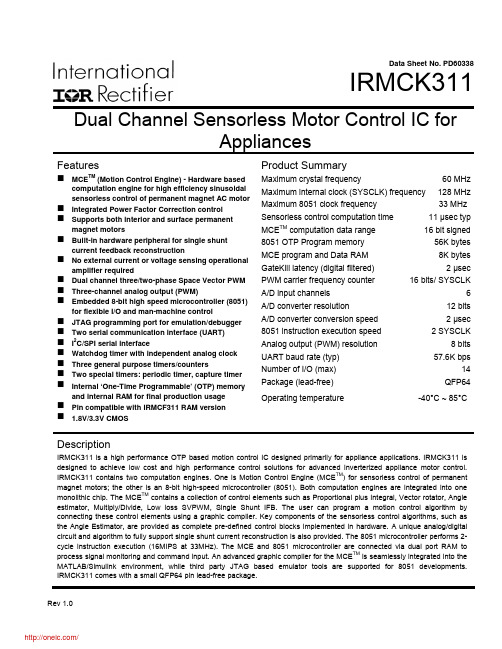
Data Sheet No. PD60338IRMCK311 Dual Channel Sensorless Motor Control IC forAppliancesFeaturesMCE TM (Motion Control Engine) - Hardware based computation engine for high efficiency sinusoidal sensorless control of permanent magnet AC motor Integrated Power Factor Correction controlSupports both interior and surface permanent magnet motorsBuilt-in hardware peripheral for single shunt current feedback reconstructionNo external current or voltage sensing operational amplifier requiredDual channel three/two-phase Space Vector PWM Three-channel analog output (PWM)Embedded 8-bit high speed microcontroller (8051) for flexible I/O and man-machine controlJTAG programming port for emulation/debugger Two serial communication interface (UART)I2C/SPI serial interfaceWatchdog timer with independent analog clockThree general purpose timers/countersTwo special timers: periodic timer, capture timer Internal ‘One-Time Programmable’ (OTP) memory and internal RAM for final production usagePin compatible with IRMCF311 RAM version1.8V/3.3V CMOS Product SummaryMaximum crystal frequency 60 MHz Maximum internal clock (SYSCLK) frequency 128 MHz Maximum 8051 clock frequency 33 MHz Sensorless control computation time 11 μsec typ MCE TM computation data range 16 bit signed 8051 OTP Program memory 56K bytes MCE program and Data RAM 8K bytes GateKill latency (digital filtered) 2 μsec PWM carrier frequency counter 16 bits/ SYSCLK A/D input channels 6 A/D converter resolution 12 bits A/D converter conversion speed 2 μsec 8051 instruction execution speed 2 SYSCLK Analog output (PWM) resolution 8 bits UART baud rate (typ) 57.6K bps Number of I/O (max) 14 Package (lead-free) QFP64 Operating temperature -40°C ~ 85°CDescriptionIRMCK311 is a high performance OTP based motion control IC designed primarily for appliance applications. IRMCK311 is designed to achieve low cost and high performance control solutions for advanced inverterized appliance motor control. IRMCK311 contains two computation engines. One is Motion Control Engine (MCE TM) for sensorless control of permanent magnet motors; the other is an 8-bit high-speed microcontroller (8051). Both computation engines are integrated into one monolithic chip. The MCE TM contains a collection of control elements such as Proportional plus Integral, Vector rotator, Angle estimator, Multiply/Divide, Low loss SVPWM, Single Shunt IFB. The user can program a motion control algorithm by connecting these control elements using a graphic compiler. Key components of the sensorless control algorithms, such as the Angle Estimator, are provided as complete pre-defined control blocks implemented in hardware. A unique analog/digital circuit and algorithm to fully support single shunt current reconstruction is also provided. The 8051 microcontroller performs 2-cycle instruction execution (16MIPS at 33MHz). The MCE and 8051 microcontroller are connected via dual port RAM to process signal monitoring and command input. An advanced graphic compiler for the MCE TM is seamlessly integrated into the MATLAB/Simulink environment, while third party JTAG based emulator tools are supported for 8051 developments. IRMCK311 comes with a small QFP64 pin lead-free package.TABLE OF CONTENTS1 Overview (5)2 IRMCK311 Block Diagram and Main Functions (6)3 Pinout (8)4 Input/Output of IRMCK311 (9)4.1 8051 Peripheral Interface Group (10)4.2 Motion Peripheral Interface Group (10)4.3 Analog Interface Group (11)4.4 Power Interface Group (11)4.5 Test Interface (12)5 Application Connections (13)6 DC Characteristics (14)6.1 Absolute Maximum Ratings (14)6.2 System Clock Frequency and Power Consumption (14)6.3 Digital I/O DC Characteristics (15)6.4 PLL and Oscillator DC Characteristics (15)6.5 Analog I/O DC Characteristics (16)6.6 Under Voltage Lockout DC Characteristics (17)6.7 AREF Characteristics (17)7 AC Characteristics (18)7.1 PLL AC Characteristics (18)7.2 Analog to Digital Converter AC Characteristics (19)7.3 Op Amp AC Characteristics (19)7.4 SYNC to SVPWM and A/D Conversion AC Timing (20)7.5 GATEKILL to SVPWM AC Timing (21)7.6 Interrupt AC Timing (21)7.7 I2C AC Timing (22)7.8 SPI AC Timing (23)7.8.1 SPI Write AC timing (23)7.8.2 SPI Read AC Timing (24)7.9 UART AC Timing (25)7.10 CAPTURE Input AC Timing (26)7.11 JTAG AC Timing (27)7.12 OTP Programming Timing (28)8 I/O Structure (29)9 Pin List (32)Dimensions (35)10 Package11 Part Marking Information (36)Information (36)12 OrderingTABLE OF FIGURESFigure 1. Typical Application Block Diagram Using IRMCK311 (5)Figure 2. IRMCK311 Internal Block Diagram (6)Figure 3. IRMCK311 Pin Configuration (8)Figure 4. Input/Output of IRMCK311 (9)Figure 5. Application Connection of IRMCK311 (13)Figure 6. Clock Frequency vs. Power Consumption (14)Figure 7 Crystal oscillator circuit (18)Figure 8 Voltage droop of sample and hold (19)Figure 9 SYNC to SVPWM and A/D conversion AC Timing (20)Figure 10 GATEKILL to SVPWM AC Timing (21)Figure 11 Interrupt AC Timing (21)Figure 12 I2C AC Timing (22)Figure 13 SPI AC Timing (23)Figure 14 SPI Read AC Timing (24)Figure 15 UART AC Timing (25)Figure 16 CAPTURE Input AC Timing (26)Figure 17 JTAG AC Timing (27)Figure 18 OTP Programming Timing (28)Figure 19 All digital I/O except motor PWM output (29)Figure 20 RESET, GATEKILL I/O (29)Figure 21 Analog input (30)Figure 22 Analog operational amplifier output and AREF I/O structure (30)Figure 23 VPP programming pin I/O structure (30)Figure 24 VSS and AVSS pin structure (31)Figure 25 VDD1 and VDDCAP pin structure (31)Figure 26 XTAL0/XTAL1 pins structure (31)TABLE OF TABLESTable 1. Absolute Maximum Ratings (14)Table 2. System Clock Frequency (14)Table 3. Digital I/O DC Characteristics (15)Table 4. PLL DC Characteristics (15)Table 5. Analog I/O DC Characteristics (16)Table 6. UVcc DC Characteristics (17)Table 7. AREF DC Characteristics (17)Table 8. PLL AC Characteristics (18)Table 9. A/D Converter AC Characteristics (19)Table 10. Current Sensing OP Amp AC Characteristics (19)Table 11. SYNC AC Characteristics (20)Table 12. GATEKILL to SVPWM AC Timing (21)Table 13. Interrupt AC Timing (21)Table 14. I2C AC Timing (22)Table 15. SPI Write AC Timing (23)Table 16. SPI Read AC Timing (24)Table 17. UART AC Timing (25)Table 18. CAPTURE AC Timing (26)Table 19. JTAG AC Timing (27)Table 20. OTP Programming Timing (28)Table 21. Pin List (32)1 OverviewIRMCK311 is a new International Rectifier integrated circuit device primarily designed as a one-chip solution for complete inverter controlled appliance dual motor control applications. Unlike a traditional microcontroller or DSP, the IRMCK311 provides a built-in closed loop sensorless control algorithm using the unique Motion Control Engine (MCE TM) for permanent magnet motors. The MCE TM consists of a collection of control elements, motion peripherals, a dedicated motion control sequencer and dual port RAM to map internal signal nodes. IRMCK311 also employs a unique single shunt current reconstruction circuit to eliminate additional analog/digital circuitry and enables a direct shunt resistor interface to the IC. The sensorless control is the same for both motors with a single shunt current sensing capability. Motion control programming is achieved using a dedicated graphical compiler integrated into the MATLAB/Simulink TM development environment. Sequencing, user interface, host communication, and upper layer control tasks can be implemented in the 8051 high-speed 8-bit microcontroller. The 8051 microcontroller is equipped with a JTAG port to facilitate emulation and debugging tools. Figure 1 shows a typical application schematic using IRMCK311.IRMCK311 is intended for volume production purpose and contains 64K bytes of OTP (One Time Programming) ROM, which can be programmed through a JTAG port. For a development purpose use, IRMCF311 contains a 48k byte of RAM in place of program OTP to facilitate an application development work. Both IRMCF311 and IRMCK311 come in the same 64-pin QFP package with identical pin configuration to facilitate PC board layout and transition to mass productionFigure 1. Typical Application Block Diagram Using IRMCK3112 IRMCK311 Block Diagram and Main FunctionsM o t i o n C o n t r o l B u sFigure 2. IRMCK311 Internal Block DiagramIRMCK311 contains the following functions for sensorless AC motor control applications:• Motion Control Engine (MCE TM )o Proportional plus Integral block o Low pass filtero Differentiator and lag (high pass filter) o Ramp o Limito Angle estimate (sensorless control) o Inverse Clark transformation o Vector rotator o Bit latch o Peak detect o Transitiono Multiply-divide (signed and unsigned)o Divide (signed and unsigned)o Addero Subtractoro Comparatoro Countero Accumulatoro Switcho Shifto ATAN (arc tangent)o Function block (any curve fitting, nonlinear function)o16-bit wide Logic operations (AND, OR, XOR, NOT, NEGATE)o MCE TM program and data memory (6K byte). Note 1o MCE TM control sequencer• 8051 microcontrollero Three 16-bit timer/counterso16-bit periodic timero16-bit analog watchdog timero16-bit capture timero Up to 36 discrete I/Oso Eleven-channel 12-bit A/DFive buffered channels (0 – 1.2V input)One unbuffered channel (0 – 1.2V input)o JTAG port (4 pins)o Up to three channels of analog output (8-bit PWM)o Two UARTo I2C/SPI porto 64K byte Note 1program One-Time Programmable memoryo2K byte data RAM. Note 2Note 1: Total size of OTP memory is 64K byte, however MCE program occupiesmaximum 8K byte which will be loaded into internal RAM at a powerup/bootprocess. Therefore only 56K byte OTP memory area is usable for 8051microcontroller.Note 2: Total size of RAM is 8K byte including MCE program, MCE data, and 8051data. Different sizes can be allocated depending on applications.3 PinoutXTAL0XTAL1P1.1/RXD P1.2/TXDVDD1VSS VDD2P1.3/SYNC/SCKP1.4/CAPP 3.6/R X D 1P 3.7/T X D 1FPWMVL FPWMUL V S SV D D 2A V D DA V S SA I N 0A R E FP 2.7/A O P W M 1P 2.6/A O P W M 0CPWMUH CPWMVH CPWMWH CPWMUL CPWMVL CPWMWL CGATEKILL VDD1VSS I F B C OI F B C +I F B C -P L L V S SP L L V D DR E S E TN CT C KP 5.3/T D IP 5.2/T D OP 5.1/T M SS D A /C S 0S C L /S O -S I /V P PP 5.0/P F C G K I L LP F C P W M V S SFGATEKILL FPWMWL VAC-VAC+VACO IPFCO IPFC+IPFC-I F B F OI F B F +I F B F -P3.0/INT2/CS1C M E X TFPWMVH FPWMUHFPWMWH A I N 1P 3.2/I N T 0Figure 3. IRMCK311 Pin Configuration4 Input/Output of IRMCK311All I/O signals of IRMCK311 are shown in Figure 4. All I/O pins are 3.3V logic interface except A/D interface pins.Figure 4. Input/Output of IRMCK3114.1 8051 Peripheral Interface GroupUART InterfaceP1.1/RXD Input, Receive data to IRMCK311, can be configured as P1.1P1.2/TXD Output, Transmit data from IRMCK311, can be configured as P1.22nd channel Receive data to IRMCK311, can be configured as P3.6 P3.6/RXD1 Input,P3.7/TXD1 Output,2nd channel Transmit data from IRMCK311, can be configured as P3.7Discrete I/O InterfaceP1.3/SYNC/SCK Input/output port 1.3, can be configured as SYNC output or SPI clock P1.4/CAP Input/output port 1.4, can be configured as Capture Timer inputP3.0/INT2/CS1 Input/output port 3.0, can be configured as external interrupt 2 or SPIchip select 1P3.2/INT0 Input/output port 3.2, can be configured as external interrupt 0Analog Output InterfaceP2.6/AOPWM0 Input/output, can be configured as 8-bit PWM output 0 withprogrammable carrier frequencyP2.7/AOPWM1 Input/output, can be configured as 8-bit PWM output 1 withprogrammable carrier frequencyCrystal InterfaceXTAL0 Input, connected to crystalXTAL1 Output, connected to crystalReset InterfaceRESET Inout, system reset, needs to be pulled up to VDD1 but doesn’t requireexternal RC time constantI2C/SPI InterfaceSCL/SO-SI/VPP Output, I2C clock output, SPI SO-SII2C Data line, Chip Select 0 of SPISDA/CS0 Input/output,P3.0/INT2/CS1 Input/output port 3.0, can be configured as external interrupt 2 or SPIchip select 1P1.3/SYNC/SCK Input/output port 1.3, can be configured as SYNC output or SPI clock 4.2 Motion Peripheral Interface GroupPWMCPWMUH Output, motor 1 PWM phase U high side gate signalCPWMUL Output, motor 1 PWM phase U low side gate signalCPWMVH Output, motor 1 PWM phase V high side gate signalCPWMVL Output, motor 1 PWM phase V low side gate signalCPWMWH Output, motor 1 PWM phase W high side gate signalCPWMWL Output, motor 1 PWM phase W low side gate signalFPWMUH Output, motor 2 PWM phase U high side gate signalFPWMUL Output, motor 2 PWM phase U low side gate signal分销商库存信息: IRIRMCK311TR。
半导体传感器ADXL288WBRDZ中文规格书

Data SheetADuM1400/ADuM1401/ADuM1402 Rev. L | Page 3 of 31REVISION HISTORY12/2016—Rev. K to Rev. LChanges to Table 1 (4)Changes to Table 2 (6)Changes to Table 3 (9)Changes to Table 4 (11)Changes to Table 5 (13)Changes to Table 6 (15)Changes to Table 7 (17)Changes to Table 9 and Table 10 (19)Changes to Ordering Guide ........................................................... 30 7/2015—Rev. J to Rev. KChanges to Table 9 and Table 10 ................................................... 19 4/2015—Rev. I to Rev. JChanged ADuM140x to ADuM1400/ADuM1401/ADuM1402..................................................................... ThroughoutChanges to Table 10 ........................................................................ 19 4/2014—Rev. H to Rev. IChange to Table 9 ............................................................................ 19 3/2012—Rev. G to Rev. HCreated Hyperlink for Safety and Regulatory ApprovalsEntry in Features Section (1)Change to PC Board Layout Section (27)Updated Outline Dimensions (30)Moved Automotive Products Section ........................................... 31 5/2008—Rev. F to Rev. GAdded ADuM1400W , ADuM1401W , and ADuM1402W Parts ...................................................................................... UniversalAdded Table 4 (11)Added Table 5 (13)Added Table 6 (15)Added Table 7 (17)Changes to Table 12 (20)Changes to Table 13 (21)Added Automotive Products Section (29)Changes to Ordering Guide ........................................................... 30 11/2007—Rev. E to Rev. FChanges to Note 1 (1)Added ADuM140xARW Change vs. Temperature Parameter ... 4 Added ADuM140xARW Change vs. Temperature Parameter (5)Added ADuM140xARW Change vs. Temperature Parameter (8)Changes to Figure 17 ...................................................................... 18 6/2007—Rev. D to Rev. E Updated VDE Certification Throughout ....................................... 1 Changes to Features and Note 1 ...................................................... 1 Changes to Figure 1, Figure 2, and Figure 3 .................................. 1 Changes to Regulatory Information Section ............................... 10 Changes to Table 7 .......................................................................... 11 Added Table 10 ................................................................................ 12 Added Insulation Lifetime Section ............................................... 20 Updated Outline Dimensions........................................................ 21 Changes to Ordering Guide ........................................................... 21 2/2006—Rev. C to Rev. D Updated Format ................................................................. Universal Added TÜV Approval ....................................................... Universal 5/2005—Rev. B to Rev. C Changes to Format ............................................................. Universal Changes to Figure 2 .......................................................................... 1 Changes to Table 3 ............................................................................ 8 Changes to Table 6 .......................................................................... 12 Changes to Ordering Guide ........................................................... 21 6/2004—Rev. A to Rev. B Changes to Format ............................................................. Universal Changes to Features .......................................................................... 1 Changes to Electrical Characteristics—5 V Operation ................ 3 Changes to Electrical Characteristics—3 V Operation ................ 5 Changes to Electrical Characteristics—Mixed 5 V/3 V or 3 V/5 V Operation ............................................................................ 7 Changes to DIN EN 60747-5-2 (VDE 0884 Part 2) Insulation Characteristics Title ........................................................................ 11 Changes to the Ordering Guide .................................................... 19 5/2004—Rev. 0 to Rev. A Updated Format ................................................................. Universal Changes to the Features.................................................................... 1 Changes to Table 7 and Table 8 ..................................................... 14 Changes to Table 9 .......................................................................... 15 Changes to the DC Correctness and Magnetic Field Immunity Section .............................................................................................. 20 Changes to the Power Consumption Section .............................. 21 Changes to the Ordering Guide .................................................... 22 9/2003—Revision 0: Initial VersionADuM1400/ADuM1401/ADuM1402Data SheetRev. L | Page 6 of 31 ELECTRICAL CHARACTERISTICS—3 V, 105°C OPERATION 1 2.7 V ≤ V DD1 ≤ 3.6 V , 2.7 V ≤ V DD2 ≤ 3.6 V; all minimum/maximum specifications apply over the entire recommended operation range, unless otherwise noted; all typical specifications are at T A = 25°C, V DD1 = V DD2 = 3.0 V . These specifications do not apply to ADuM1400W , ADuM1401W , and ADuM1402W automotive grade versions. Table 2.ParameterSymbol Min Typ Max Unit Test Conditions DC SPECIFICATIONSInput Supply Current per Channel, QuiescentI DDI (Q) 0.26 0.31 mA Output Supply Current per Channel, QuiescentI DDO (Q) 0.11 0.14 mA ADuM1400 Total Supply Current, Four Channels 2DC to 2 MbpsV DD1 Supply CurrentI DD1 (Q) 1.2 1.9 mA DC to 1 MHz logic signal freq. V DD2 Supply CurrentI DD2 (Q) 0.5 0.9 mA DC to 1 MHz logic signal freq. 10 Mbps (BRW and CRW Grades Only)V DD1 Supply CurrentI DD1 (10) 4.5 6.5 mA 5 MHz logic signal freq. V DD2 Supply CurrentI DD2 (10) 1.4 2.0 mA 5 MHz logic signal freq. 90 Mbps (CRW Grade Only)V DD1 Supply CurrentI DD1 (90) 37 65 mA 45 MHz logic signal freq. V DD2 Supply CurrentI DD2 (90) 11 15 mA 45 MHz logic signal freq. ADuM1401 Total Supply Current, Four Channels 2DC to 2 MbpsV DD1 Supply CurrentI DD1 (Q) 1.0 1.6 mA DC to 1 MHz logic signal freq. V DD2 Supply CurrentI DD2 (Q) 0.7 1.2 mA DC to 1 MHz logic signal freq. 10 Mbps (BRW and CRW Grades Only)V DD1 Supply CurrentI DD1 (10) 3.7 5.4 mA 5 MHz logic signal freq. V DD2 Supply CurrentI DD2 (10) 2.2 3.0 mA 5 MHz logic signal freq. 90 Mbps (CRW Grade Only)V DD1 Supply CurrentI DD1 (90) 30 52 mA 45 MHz logic signal freq. V DD2 Supply CurrentI DD2 (90) 18 27 mA 45 MHz logic signal freq. ADuM1402 Total Supply Current, Four Channels 2DC to 2 MbpsV DD1 or V DD2 Supply CurrentI DD1 (Q), I DD2 (Q) 0.9 1.5 mA DC to 1 MHz logic signal freq. 10 Mbps (BRW and CRW Grades Only)V DD1 or V DD2 Supply CurrentI DD1 (10), I DD2 (10) 3.0 4.2 mA 5 MHz logic signal freq. 90 Mbps (CRW Grade Only)V DD1 or V DD2 Supply CurrentI DD1 (90), I DD2 (90) 24 39 mA 45 MHz logic signal freq. For All ModelsInput CurrentsI IA , I IB , I IC , I ID , I E1, I E2 −10 +0.01 +10µA 0 V ≤ V IA , V IB , V IC , V ID ≤ V DD1 or V DD2, 0 V ≤ V E1, V E2 ≤ V DD1 or V DD2 Logic High Input ThresholdV IH , V EH 1.6 V Logic Low Input ThresholdV IL , V EL 0.4 V Logic High Output VoltagesV OAH , V OBH , V OCH , V ODH (V DD1 or V DD2) − 0.1 3.0 V I Ox = −20 µA, V Ix = V IxH (V DD1 or V DD2) − 0.4 2.8 V I Ox = −3.2 mA, V Ix = V IxH Logic Low Output Voltages V OAL , V OBL , V OCL , V ODL 0.0 0.1 VI Ox = 20 µA, V Ix = V IxL 0.04 0.1 VI Ox = 400 µA, V Ix = V IxL0.2 0.4 V I Ox = 3.2 mA, V Ix = V IxLSWITCHING SPECIFICATIONSADuM1400ARW /ADuM1401ARW /ADuM1402ARWMinimum Pulse Width 3PW 1000 ns C L = 15 pF, CMOS signal levels Maximum Data Rate 41 Mbps C L = 15 pF, CMOS signal levels Propagation Delay 5t PHL , t PLH 50 75 100 ns C L = 15 pF, CMOS signal levels Pulse Width Distortion, |t PLH − t PHL |5PWD 40 ns C L = 15 pF, CMOS signal levels Change vs. Temperature11 ps/°C C L = 15 pF, CMOS signal levels Propagation Delay Skew 6t PSK50 ns C L = 15 pF, CMOS signal levels Channel-to-Channel Matching 7 t PSKCD /t PSKOD50 ns C L = 15 pF, CMOS signal levels。
单晶硅压力变送器说明书
图 3 单晶硅变送器墙面安装
图 4 单晶硅压力变送器管道安装
安装
昌晖仪表 /
3 / 26
单晶硅压力变送器/单晶硅差压变送器说明书
为了正确安装单晶硅压力变送器,必须遵循以下几点: 1、引压管道尽可能短,并避免急弯折。 2、引压管道的安装坡度不应小于 1:12,以免引起沉淀。 3、引压管道在连接到变送器前,必须用压缩空气吹一遍,最好用被测介质冲洗一遍。 4、如果介质是液体,则应彻底放空引压管道。 5、引压管道的布局,应使得被测液体中的气泡或被测气体中的沉淀物能回流到过程管道中。 6、安装过程管道时,不得有任何泄露。
菜单操作 …………………………………………………………………………………………………… 6 操作说明 ……………………………………………………………………………………………… 8 按键定义 ……………………………………………………………………………………………… 8 菜单启动与退出 ……………………………………………………………………………………… 8 菜单浏览 ……………………………………………………………………………………………… 9 菜单选择 ……………………………………………………………………………………………… 9 数据输入 ……………………………………………………………………………………………… 9
使用说明书压力差压智能变送器operationinstruction13菜单启动与退出13变量查看13模拟量程加压零位迁移15模拟量程加压满位设定16模拟量程零位设定17模拟量程满位设定18数字零点调整20模拟量程平行迁移21阻尼设定23显示类型选择23单位选择24特性函数选择24维护26修理26单晶硅压力变送器单晶硅差压变送器说明书前言yrer100系列智能单晶硅压力变送器单晶硅差压变送器是采用高精度硅传感器技术新型智能高精度变送器基于通过微处理器的电子部件实现与现场设备通信
AG9311中文规格说明书2020新版.PDF
AG9311带PD3.0 Type C转HDMI转换器AG9311AG9311Type-C转HDMI转换器数据表修订历史PS:本中文规格书由第三方翻译软件自动翻译,权威信息请以原厂英文版规格书为准。
2AG9311Type-C转HDMI转换器数据表索引1.概述 (5)2.特性 (5)3.设备信息 (6)4.应用 (6)5.系统框图 (7)6.管脚映射和描述 (8)7.规格明细 (15)i. 绝对最大额定值绝对最大额定值 (15)ii. 直流特性/工作条件 (15)iii. 交流特性 (16)8. 包装和标记规范 (19)3AG9311Type-C转HDMI转换器数据表图目录图1 Type-C转HDMI 适配器的应用 (6)图2系统框图 (7)图3 AG9311MAQ引脚映射 (8)图4 AG9311-MCQ引脚映射 (12)图5 AG9311-MAQ包装尺寸..... (20)图6 AG9311-MCQ包装尺寸 (21)表格列表表1引脚说明........ (9)表2引脚说明....... (12)表3绝对最大额定值 (15)表4数字I/O规范.... (16)表5显示端口输入 (16)表6显示端口辅助通道I/O规格. (17)表7 USB I/O规格 (18)表8 USB PD规格 (18)4AG9311Type-C转HDMI转换器数据表一、概述ALGOLTEK AG9311是一款高度集成的解决方案,通过USB Type-C将视频和音频从DisplayPort alternate mode传输到HDMI输出。
AG9311支持各种@1.62Gbps、2.7Gbps和5.4Gbpsup通到DisplayPort 1.2,支持1路2路通道;HDMI支持4K/2K@30Hz输出。
用户可以轻松地将AG9311集成到视频转换适配器和扩展坞上。
二、特性1、显示符合 DisplayPort specification Revision 1.2支持1.62(RBR)/2.7(HBR)/5.4(HBR2)Gbps数据速率支持1/2线路配置支持下行扩频时钟(SSC)-支持I2S总线音频提取2、HDMIHDMI 高清多媒体接口符合HDMI1.4和HDCP1.4规范支持高达3Gbps的TMD支持分辨率高达4kx2k@30Hz输出支持HDCP键预先编程兼容EDID和MCCS支持采样率48kHz/44.1KHz/32KHz的LPCM双通道3、USB Type-C PD支持显示端口备用模式协议DisplayPort Alternate符合USB PD3.0集成Type-C RP and RD电阻器支持2个 USB Type-C端口支持USB宣称集成USB2.0全速5AG9311Type-C转HDMI转换器数据表4、单片机系统及接口集成16位单片机集成用于固件升级的64KB闪存支持I2C主/从、UART、USB2.0全速支持3通道8 bit分辨率ADC5、电源操作和ESD3.3V:3V至3.6V操作1.2V:1.08至1.32V运行1.2V核心电源和3.3V I/O电源HBM 2KV ESD性能三、设备信息四、应用USB Type-C 转换器USB Type-C扩展坞6AG9311Type-C转HDMI转换器数据表五、系统框图7AG9311Type-C转HDMI转换器数据表六、管脚映射和描述图3 AG9311-MAQ引脚映射8AG9311Type-C转HDMI转换器数据表表1基本说明9AG9311Type-C转HDMI转换器数据表10AG9311Type-C转HDMI转换器数据表11AG9311Type-C转HDMI转换器数据表图4 AG9311-MCQ引脚映射表2引脚说明12AG9311 Type-C转HDMI转换器数据表13AG9311 Type-C转HDMI转换器数据表14AG9311Type-C转HDMI转换器数据表七、规格明细1.绝对最大额定值表3绝对最大额定值2.直流特性/工作条件15AG9311Type-C转HDMI转换器数据表Table 4 Digital I/O Specification表4数字I/O规范3.交流特性显示端口主链交流特性表5显示端口输入定时16AG9311Type-C转HDMI转换器数据表显示端口AUX-CH AC特性表6显示端口辅助通道I/O规格17AG9311Type-C转HDMI转换器数据表USB PD BMC接收器规范要求表7 USB I/O规格USB PD BMC发射机规范要求表8 USB PD规格AG9311Type-C转HDMI转换器数据表八、包装和标记规范标记19AG9311Type-C转HDMI转换器数据表包装尺寸AG9311-MAQ: QFN-64L 8x8mm(E-PAD SIZE:181x18*MIL)图5 AG9311-MAQ包装尺寸20AG9311Type-C转HDMI转换器数据表AG9311-MCQ:QFN-48L 6x6mm(电子板尺寸:185x18*MIL)Figure 6 AG9311-MCQ Package Dimension图6 AG9311-MCQ包装尺寸21。
loctite乐泰3491UV胶水中文版MSDS
大鼠
NOAEL=0,225
吸入
14 d
mg/kg
大鼠
测试方法
世界经济合作与发展组织 准则 407 (啮齿类动物28天反复经口 毒性试验) 世界经济合作与发展组织 准则 412 (反复吸入毒性试验21/14天)
MSDS-No.: 153581 V001.5
LOCTITE 3491 UNLB 25ML SYRINGE
第十二部分 生态学资料
生态信息: 禁止排入下水道、地表水、地下水。 对水生生物有毒。 可能在水生环境中造成长期不利影响。
生态毒性: 无资料。
持久性和降解性: 完全生物降解能力:
无资料。
生物累积潜力: 无资料。
第 7 页 共 11 页
MSDS-No.: 153581 V001.5
其他危害效应: 无资料。
企业信息:
汉高(中国)投资有限公司
张衡路928号
201203
中国上海市浦东新区
中国
电话: 传真:
+86-21-2891 8000 +86-21-2891 5137
生效日期:
03.12.2012
应急信息:
应急电话:+86 532 8388 9090 (24小时)。
第二部分 危险性概述
物质或混合物的分类根据GB 13690-2009 (化学品分类和危险性公示通则):
急性毒性研 接触时间
生物种类
测试方法
究
Daphnia 48 h
大型蚤
世界经济合作与
发展组织 准则
202
(蚤类急性活动
抑制试验)
Algae
72 h
近头状伪蹄形藻
世界经济合作与
产品规格说明书(键合合金丝)

红色标签。产品在使用时必须要求在洁净的区域内打开检验和使用,严禁在未经过的净化 的工作环境中打开,避免出现产品污染现象,造成产品的质量问题,带来不必要的损失。 5、产品存放的环境要求通风、干燥、明亮、清洁和通畅,适宜于产品的贮存条件为温度16℃26℃,湿度≤75%,贮存的有效期为三个月。
A.法兰直径Flange diameter B. 管芯直径Core diameter
C.内径 Internal diameter D.总宽度Overall width E.绕线宽度Width over windings
广东佳博电子科技有限公司 键合合丝规格说明书
第3页
九、产品拿取方法、储存环境
1、在净化车间内将产品放平于桌面,用左手的拇指与食指按住吸塑盒底,用右手轻轻的将吸 塑盒盖向上提(如图9-1);
绕线宽度widthoverwindings广东佳博电子科技有限公司第3页键合合丝规格说明书图91图92图93十产品检查项目1在净化车间内依据生产计划单及合格产品数量打印相应数量的标签将标签贴于金丝吸塑盒盖正前面上标签内容包括单轴长度型号批号包装编号技术要求等内容
一、产品适用范围
广东佳博电子科技有限公司 键合合金丝规格说明书
四、产品规格
根据合金丝的直径(mm)分为0.018 0.019 0.020 0.021 0.022 0.028 0.030 0.032 0.033 0.035 0.038 0.040 0.045 0.050 个直径规格。
- 1、下载文档前请自行甄别文档内容的完整性,平台不提供额外的编辑、内容补充、找答案等附加服务。
- 2、"仅部分预览"的文档,不可在线预览部分如存在完整性等问题,可反馈申请退款(可完整预览的文档不适用该条件!)。
- 3、如文档侵犯您的权益,请联系客服反馈,我们会尽快为您处理(人工客服工作时间:9:00-18:30)。
Positive Power Supply: Bypass with 0.1µF//0.01µF low ESR capacitors.
M9999-092606 hthtpbw://hoenlpe@icm.ciocmrel/.com or (408) 955-1690
2
Micrel, Inc.
Precision Edge® SY89311U
Absolute Maximum Ratings(1)
Supply Voltage (VCC) .................................. –0.5V to +6.0V Input Voltage (VIN) ......................................... –0.5V to VCC LVPECL Output Current (IOUT)
Condition
VCC
Power Supply Voltage
LVPECL LVPECL PECL ECL LVECL LVECL
IEE
Power Supply Current
Max. VCC, no load
IIH
Input HIGH Current
VIN = VIH
IIL
Input LOW Current
• fMAX > 3.0GHz • < 20ps output-to-output skew • < 200ps tr / tf • < 300ps propagation delay ■ 100K compatible I/O ■ Wide temperature range: –40°C to +85°C ■ Available in ultra-small 8-pin MLF® (2mm × 2mm) package
Lead Finish
Sn-Pb
Pb-Free NiPdAu
PIN DESCRIPTION
Pin Number 1, 2, 3, 4
5 6 7 8
Pin Name Q0, /Q0, Q1, /Q1
VEE, Exposed Pad
/IN
IN
VCC
Type 100K Output
Negative Power Supply
M9999-092606 hthtpbw://hoenlpe@icm.ciocmrel/.com or (408) 955-1690
1
Rev.: D Amendment: /0 Issue Date: September 2006
Micrel, Inc.
Precision Edge® SY89311U
Symbol
Parameter
Condition
Min
Typ
Max Units
VOH VOL VIH VIL VIHCMR
Output HIGH Voltage Output LOW Voltage Input HIGH Voltage Input LOW Voltage Input HIGH Voltage Common Mode Range
BLOCK DIAGRAM
IN PECL /IN
Q0
/Q0 PECL
Q1
/Q1
DESCRIPTION
Precision Edge®
The SY89311U is a precision, high-speed 1:2 differential fanout buffer. Having within-device skews and output transition times significantly improved over the EL11V, the SY89311U is ideally suited for those applications which require the ultimate in AC performance in a small package.
Negative Power Supply: VEE and exposed pad must be tied to most negative supply. For PECL/LVPECL connect to ground.
Differential PECL/ECL Input: Internal 75kΩ pull-up and pull-down resistors. If left floating, pin defaults to VCC/2. When not used, this input can be left open. See “Input Interface Applications” section for single-ended inputs.
30
44
mA
150
µA
0.5
µA
–150
µA
1.0
pF
(100K) ECL/LVECL DC ELECTRICAL CHARACTERISTICS
VCC = +2.5V ±5% or +3.3V ±10% or +5.0V ±10% and VEE = 0V; VCC = 0V and VEE = –2.5V ±5% or –3.3V ±10% or –5.0V ±10%; RL = 50Ω to VCC–2V; TA = –40°C to +85°C, unless otherwise noted.
Input Current Source or sink current on IN, /IN .......................... ±50mA
Lead Temperature (soldering, 20 sec.) ................... +260°C Storage Temperature (TS) ....................... –65°C to +150°C
Ambient Temperature (TA) ......................... –40°C to +85°C Package Thermal Resistance, Note 3
MLF™ (θJA) Still-Air ................................................................. 93°C/W 500lfpm ............................................................... 87°C/W
The differential inputs can accept 10/100K ECL/PECL signals (external termination required) and the outputs are 100K ECL/PECL compatible.
Precision Edge is a registered trademark of Micrel, Inc. MicroLeadFrame and MLF are registered trademarks of Amkor Technology, Inc.
Continuous ............................................................. 50mA Surge .................................................................... 100mA
The differential inputs of the SY89311U employ clamping circuitry to maintain stability under open input conditions. If the inputs are left open, the Q outputs will be LOW.
Operating Ratings(2)
Supply Voltage |VCC–VEE| .................. +2.375V to +2.625V ............................................................ +3.0V to +3.6V ............................................................ +4.5V to +5.5V
IN VIN = VIL /IN VIN = VIL
CIN
Input Capacitance
Min Typ Max Units
2.375 2.5 2.625 V
3.0
3.3
3.6
V
4.5
5.0
5.5
V
–5.5 –5.0 –4.5
V
–3.6 –3.3 –3.0
V
–2.625 –2.5 –2.375 V
PACKAGE/ORDERING INFORMATION
Q0 1 /Q0 2 Q1 3 /Q1 4