Simplified design of common-mode chokes for reduction of motor ground currents in inverter drives
仪表放大器输入RFI保护

G1
G2
B See for manufactures of x2y capacitors
图4:X2Y®电容静电模型
G1和G2引脚在器件内部相连。X2Y电容的内部板结构形成一种集成电路,具有一些有趣 的特性。从静电角度来看,三个电节点构成两个电容,这两个电容共享G1和G2引脚。制 造工艺会自动严格匹配这两个电容。此外,X2Y结构包含有效的自动变压器/共模扼流圈。 因此,当共模滤波器使用这类器件时,与类似RC滤波器相比,高于滤波器转折频率的共 模信号衰减幅度更大。因此,通常无需电容C3,进而节省了成本和电路板空间。 图5A所示为传统的RC共模滤波器,而图5B所示为采用X2Y器件的共模滤波器电路。图6比 较了这两种滤波器的RF衰减性能。
C1·C2 C1 + C2 + C3
图1:代码跃迁噪声(折合到输入端噪声)及其对ADC传递函数的影响
假设C3 >> C1,由此得到CM滤波器带宽为1/2πR1⋅C1,而DM滤波器带宽则大约为1/4πR1⋅C3。 总体DM滤波器带宽应至少为输入信号带宽的100倍。滤波器元件应对称安装在具有较大面 积接地层的电路板上,并且应该靠近仪表放大器的输入端,以便获得最佳性能。 图2显示了一系列适合各种不同仪表放大器的此类滤波器。RC元件应根据不同仪表放大器 进行定制,具体如表中所示。选择这些滤波器元件是为了实现低EMI/RFI灵敏度和低噪声 增长的合理平衡(与无滤波器的相应仪表放大器相比)。 要测试配置的EMI/RFI灵敏度,可以向输入电阻施加1 V p-p CM信号,如上所述。当 AD620等常用仪表放大器在增益为1000下工作时,20 MHz范围内观测到的最大RTI输入失 调电压漂移为1.5 V。在AD620滤波器示例中,差分带宽约为400 Hz。
英语作文-揭秘集成电路设计中的设计规则与布局约束

英语作文-揭秘集成电路设计中的设计规则与布局约束Integrated circuit (IC) design is a complex process that involves various design rules and layout constraints. In this article, we will delve into the secrets of IC design and explore the key considerations in designing and laying out integrated circuits.To begin with, one of the fundamental design rules in IC design is the minimum feature size. This refers to the smallest dimension that can be reliably manufactured on a chip. As technology advances, the minimum feature size decreases, allowing for more transistors to be packed onto a single chip. Designers must adhere to these rules to ensure the manufacturability and functionality of the IC.Another important design rule is the spacing between different components on the chip. This is known as the minimum spacing rule and ensures that there is sufficient isolation between adjacent components. Violating this rule can lead to interference and crosstalk, which can severely impact the performance of the IC. Designers must carefully consider the spacing requirements and optimize the layout to minimize any potential issues.Furthermore, the design of power distribution networks is crucial in IC design. Efficient power delivery is essential to ensure the proper functioning of the circuitry. Designers must consider factors such as voltage drop, current density, and thermal management when designing the power distribution network. By carefully analyzing and optimizing the power delivery system, designers can enhance the overall performance and reliability of the IC.In addition to design rules, layout constraints play a vital role in IC design. One such constraint is the placement of components on the chip. Proper component placement is essential to minimize signal delays and optimize the overall performance of the IC. Designers must consider factors such as signal integrity, power consumption, and thermal considerations when determining the optimal component placement.Another important layout constraint is the routing of interconnects. Interconnect routing refers to the process of connecting different components on the chip using metal traces. Designers must carefully plan and optimize the routing to minimize signal delays, reduce power consumption, and ensure proper signal integrity. Advanced routing algorithms and techniques are employed to achieve efficient and reliable interconnects.Moreover, the consideration of design for manufacturing (DFM) rules is crucial in IC design. DFM rules ensure that the design can be manufactured with high yield and reliability. Designers must consider factors such as lithography constraints, process variations, and mask alignment accuracy when designing the IC. By incorporating DFM rules into the design process, designers can minimize manufacturing issues and improve the overall yield of the IC.In conclusion, the design rules and layout constraints in integrated circuit design are essential for ensuring the manufacturability, functionality, and performance of the IC. Designers must carefully adhere to these rules and constraints while considering factors such as minimum feature size, component spacing, power distribution, component placement, interconnect routing, and design for manufacturing. By following these guidelines, designers can create efficient, reliable, and high-performance integrated circuits.。
共模扼流圈的参数及选型

共模扼流圈的参数及选型Common mode chokes are essential components in electronic circuits to reduce electromagnetic interference. 共模抑制器是电子电路中必不可少的元件,用于减少电磁干扰。
They are designed to suppress common mode noise by providing a high impedance path for common mode currents while allowing differential mode signals to pass through unaffected. 它们的设计是为了通过为共模电流提供高阻抗路径来抑制共模噪声,同时允许差分模信号无受影响地通过。
Common mode chokes consist of two windings wound on a ferromagnetic core, which can be customized based on the specific requirements of the application. 共模抑制器由绕在铁磁芯上的两个绕组组成,可以根据应用的具体要求进行定制。
The parameters and selection of common mode chokes are crucial in ensuring optimal performance and noise suppression in electronic circuits. 共模抑制器的参数和选择对于确保电子电路的最佳性能和噪声抑制至关重要。
When selecting common mode chokes, it is important to consider factors such as impedance, current rating, frequency range, and temperature stability. 在选择共模抑制器时,需要考虑阻抗、电流额定值、频率范围和温度稳定性等因素。
Silicon Laboratories 微控制器低功耗选择指南说明书

How to Pick the Right Microcontroller Based on Low-PowerSpecificationsIntroductionChoosing the right ultra-low-power microcontroller (MCU) for your next embedded design can be a confusing task when you compare claimed current consumption specifications in a myriad of data sheets provided by MCU vendors. In many cases, developers initially scan the first page of a data sheet as a reference point to gain basic information about an MCU, including peripherals, operating speed, package information, number of GPIOs and power characteristics. This approach works well to assess an MCU’s overall functionality, but it is not particularly useful when trying to gauge low-power characteristics.To get a broader view of an M CU’s true low-power operation, developers must take into consideration current consumption, state retention, wake-up time, wake-up sources and peripherals that are capable of operating while in low-power mode. Developers must compare a common operating mode to gain a balanced, apples-to-apples comparison among competing low-power MCUs. It is also important to take into consideration any additional functionality or peripherals that can reduce total system power and available evaluation tools that can make an engineer’s job easier.Microcontroller vendors will usually list the lowest power achievable on the first page of the data sheet. Although the device may be capable of achieving the specification in the data sheet, the actual operating mode may not be practical and useful in a real-world application. Some of the non-advertised features of the lowest power mode may include a very slow wake time, no state or RAM retention, or a reduced operating voltage range.To get around the variety of low-power specifications, developers must identify a common operating mode consisting of two sections: electrical specifications and low-power functionality.Comparing Electrical Specifications of MicrocontrollersThe electrical specifications are available in the data sheet, but determining which specifications are relevant may require some digging. Usually the electrical specifications are organized by vendor-specific power mode. This makes assessment slightly more difficult, as it requires knowledge and familiarity with the functionality of each power mode.In general, it is beneficial to define a set of operating conditions and then map them to a power mode. For example, the developer might define the following set of operating conditions:∙Sleep mode current consumption with state and RAM retentiono All other peripherals disabled∙Sleep mode current consumption with RTC running with state and RAM retentiono RTC enabled and running all other peripherals disabled.∙Wake time∙Supply voltage rangeOnce the operating conditions are clearly defined, it should be easy to determine the applicable vendor-specific power mode.Additional Low-Power FunctionalityThe second section, low-power functionality, is not as easy to locate in the vendor’s documentation and may be spread across the data sheet and reference manual. Examples of low-power functionality include: ∙Available wake sources∙How code resumes execution∙Peripherals capable of operating in sleep mode.Once the common operating mode has been clearly defined, developers can begin to examine the documentation in more detail.While going through this exercise of compiling data, keep in mind that there may be some MCU-specific features that can further optimize an application for ultra-low power. Optimizations may reduce bill of material (BOM) costs, provide longer product life or provide greater design flexibility. For example, an on-chip dc-dc converter can efficiently provide power to the system and decrease power consumption. This can enable the use of smaller batteries, which will decrease the overall BOM costs, or provide power budget flexibility. A variety of wake sources can provide design flexibility and allow the microcontroller to stay in the lowest power mode as long as possible, further reducing the average current consumption of the application.Allowing firmware to scale the internal supply voltage is another optimization knob available to the developer. If an MCU is operating at a slow frequency, it may be possible to decrease the supply voltage and save power. Selective clock gating allows hardware blocks to be disconnected from the active circuits, preventing inactive peripherals from consuming power. These types of features are not comprehended by supply current specifications that are commonly used to rank low-power MCUs, but are critical to achieving the lowest overall system power consumption.Reducing Complexity Using ToolsAs MCUs become more and more configurable to achieve the lowest power consumption, they also can become more complex. To cope with this increased complexity, developers should take a close look at the evaluation platforms available for an MCU and the overall ease of implementing a solution. For example, the development board and software tools used to program the MCU should be intuitive and easy-to-use. Hardware that is difficult to understand or use is not likely to lead to an easy firmware development process. From a firmware perspective, MCU vendors should supply firmware examples that can recreate specifications from the data sheet. If advertised current consumption specifications cannot be recreated on an evaluation platform, it is likely that it will be just as difficult (if not impossible) to configure the MCU to achieve these numbers on custom hardware. Giving customers a variety of code examples that can be used as a starting point for their code development can reduce time-to-market and help engineers learn to use a device.Graphical configuration tools can aid in development and help the developer gain a deeper understanding of an MCU. When developing low-power applications, it is helpful to know where the total consumed power is going. This information is useful because it highlights what aspect of a design needs to be further optimized and can also help the developer understand the overall architecture of the device. Ideally, low-power configuration tools could give tips on further reducing power as well as highlight any configuration errors that were detected throughout the configuration process. For example, the Power Estimator utility within Silicon Labs’ AppBuilder graphical configuration tool provides Power Tips that give configuration guidance and a power-budget pie chart showing how much power is consumed and which peripherals are consuming the power. As configuration changes are made, the pie chart automatically updates.Figure 1. Power Estimator Enables Developers to Optimize for Lowest Current Consumption To facilitate the microcontroller comparison process, the following table provides a list of common operating modes, as well as system-level optimizations and development tools available for Silicon Labs’32-bit SiM3L1xx MCUs based on the ARM® Cortex™-M3 core.SummaryEvaluating and selecting a microcontroller for a low-power application requires more than a quick scan of the first page of the data sheet. Determining which MCU provides the lowest overall system power requires developers to know the device’s supply current specifications, as well as any system-level optimizations that can reduce the overall supply current.Unfortunately, each MCU vendor specifies operating conditions differently and in some cases advertises a low-power number that is available in an unusable mode. Using a common operating mode to compare MCUs will prevent developers from being misled by vendor claims of ultra-low-power operation.Once the electrical characteristics of a device are understood and quantified, developers should take a look at the evaluation platform and software tools available. These considerations are crucial in getting an engineering team up and running quickly and should be included in the final microcontroller selection process. Find out more about Silicon Labs’ microcontrollers, including 8-bit and 32-bit MCUs at/mcu.# # #Silicon Labs invests in research and development to help our customers differentiate in the market with innovative low-power, small size, analog intensive, mixed-signal solutions. Silicon Labs' extensive patent portfolio is a testament to our unique approach and world-class engineering team. Patent: /patent-notice© 2013, Silicon Laboratories Inc. ClockBuilder, DSPLL, Ember, EZMac, EZRadio, EZRadioPRO, EZLink, ISOmodem, Precision32, ProSLIC, QuickSense, Silicon Laboratories and the Silicon Labs logo are trademarks or registered trademarks of Silicon Laboratories Inc. ARM and Cortex-M3 are trademarks or registered trademarks of ARM Holdings. ZigBee is a registered trademark of ZigBee Alliance, Inc. All other product or service names are the property of their respective owners.。
反激式开关电源外文翻译
Measurement of the Source Impedance of Conducted Emission Using Mode Separable LISN: Conducted Emission of a Switching Power SupplyJUNICHI MIY ASHITA,1 MASAYUKI MITSUZAW A,1 TOSHIYUKI KARUBE,1KIYOHITO Y AMASAW A,2 and TOSHIRO SA TO21Precision Technology Research Institute of Nagano Prefecture, Japan2Shinshu University, JapanSUMMARYIn the procedure for reducing conducted emissions, it is helpful to know the noise source impedance. This paper presents a method of measuring noise source complex impedances of common and differential mode separately. We propose a line impedance stabilization network (LISN) to measure common and differential mode noise separately without changing LISN impedances of each mode. With this LISN, conducted emissions of each mode are measured inserting appropriate impedances at the equipment under test (EUT) terminal of the LISN. Noise source complex impedances of switching power supply are well calculated from measured results. © 2002 Scripta Technica, Electr Eng Jpn, 139(2): 72 78, 2002; DOI 10.1002/eej.1154Key words:Conducted emission; noise terminal voltage; noise source impedance; line impedance stabiliza-tion network (LISN); EMI.1. IntroductionSwitching power supplies are employed widely in various devices. High-speed on/off operation is accompa-nied by harmonic noise that may cause electromagnetic interference (EMI) with communication devices and other equipment. To prevent the interference, methods of meas-urement and limit values have been set for conducted noise (~30 MHz) and radiated noise (30 to 1000 MHz). Much time and effort are required to contain the noise within the limit values; hence, the efficiency of noise removal tech-niques is an urgent social problem. Understanding of the mechanism behind noise generation and propagation is necessary in order to develop efficient measures. In particu-lar, the propagation of conducted noise must be investi-gated.Modeling and analysis of equivalent circuits have been carried out in order to investigate conducted noise caused by switching [1, 2]. However, the stray capacitance and other circuit parameters of each device must be known in order to develop an equivalent circuit, which is not practicable in the field of noise removal. On the other hand, noise filters and other noise-removal devices do not actually provide the expected effect [3, 4], which is explained by the difference between the static characteristics measured at an impedance of 50 Ω, and the actual impedance. Thus, it is necessary to know the noise source impedance in order to analyze the conducted noise.Regulations on the measurement of noise terminal voltage [5] suggest using LISN; in particular, the vector sum (absolute voltage) of two propagation modes, namely, common mode and differential mode, is measured in terms of the frequency spectrum. Such a measurement, however, does not provide phase data, and propagation modes cannot be separated; therefore, the noise source impedance cannot be derived easily. There are publications dealing with the calculation of the noise source impedance; for example, common mode is only considered as the principal mode, and the absolute value of the noise source impedance for the common mode is found from the ground wire current and ungrounded voltage [6], or mode-separated measure-ment is performed by discrimination between grounded and ungrounded devices [7]. However, measurement of the ground wire current is impossible in the case of domestic single-phase two-line devices. The complex impedance can be found using an impedance analyzer in the nonoperating state, but its value may be different for the operating state. Thus, there is no simple and accurate method of measuring source noise impedance as a complex impedance.© 2002 Scripta TechnicaElectrical Engineering in Japan, V ol. 139, No. 2, 2002Translated from Denki Gakkai Ronbunshi, V ol. 120-D, No. 11, November 2000, pp. 1376 1381The authors assumed that the noise source impedance could be found easily using only a spectrum analyzer, provided that the noise could be measured separately for each mode, and the LISN impedance could be varied. For this purpose, a LISN with a balun transformer was devel-oped to ensure noise measurement, with the common mode and differential mode strictly separated. An appropriate known impedance is inserted at the EUT (equipment under test) terminals, and the noise source impedance is found from the variation of the noise level. This method was used to measure the conducted noise of a switching power sup-ply, and it was confirmed that the noise source impedance could be measured as a complex impedance independently for each mode. Thus, significant information for noiseremoval and propagation mode analysis was acquired.This paper presents a new method of measuring the noise source impedance of conducted emission using mode-separable LISN.2. Separate Measurement for Common Mode andDifferential ModeThe conventional single-phase LISN circuit for measurement of the noise terminal voltage is shown in Fig.1. The power supply is provided with high impedance by a 50-µH reactor, and a meter with an input impedance of 50Ω is connected between one line and the ground via a high-pass capacitor, and another line is terminated by 50 Ω. Thus, the LISN impedance as seen at the EUT is 100 Ω in the differential mode, and 25 Ω in the common mode. The measured value is the vector sum of both modes, and the noise must be found separately in order to find the noise source impedance for each mode. There is LISN with Y-to-delta switching to provide mode separation [8], but its impedance is 150 Ω, giving rise to a problem of data compatibility with 50-Ω LISN. Thus, a new mode-separa-ble LISN was developed as shown in Fig.2. The circuit is identical to that in Fig. 1 from the power supply through the high-pass capacitor. Switching of the connection pattern ensures measurement with one line of the balun transformer terminated by 50 Ω, and another line connected to the meter.In Fig. 2, the secondary side of the 2:1 balun trans-former is terminated by 50 Ω, while the primary side has 200 Ω; in the differential mode, the impedance (line-to-line) is 100 Ω since 200 Ω at the high-pass capacitor is connected in parallel. With the switch set at D, the meter is connected to the secondary side of the balun transformer. The voltage is one-half that of the line-to-line voltage, and measurement is performed in the standard way.The common mode current flows from both sides of the balun transformer via the middle tap to the 50-Ω termi-nal. The currents in the windings are antiphase, and no voltage is generated at the secondary side. Therefore, the impedance of the primary side is the terminal resistance of the tap. Since this impedance is connected in parallel to 50Ω (two 100 Ω in parallel) at the high-pass capacitor, the impedance between the common line and ground is 25 Ω. With the switch set at C, the meter is connected to the middle tap of the balun transformer, and the common-mode voltage is the line-to-ground voltage.3. Measurement of Noise Source Impedance3.1 Measurement circuit and calculationThough the propagation routes are different in the two modes, propagation from the noise source to the LISN can be represented in a simplified way as shown in Fig. 3. In the initial measurement, the load impedance Z L is the LISN impedance. Z L can be varied by inserting a knownimpedance at the EUT terminals. Consider three load im-Fig. 1. Standard 50-Ω/50-µH LISN.Fig. 2.Mode-separable LISN.Fig. 3. Schematic circuit of noise propagation.pedances, namely, LISN only and LISN with two different impedances inserted, Z L 1(R 1 + jX 1), Z L 2(R 2 + jX 2), andZ L 3(R 3+ jX 3). Using the values I 1, I 2, I 3 (scalars) measured in the three cases, Z 0(R 0 + jX 0) is found. Since V 0 = |Z L | × I ,the following expressions can be derived:From the above,Here a , b , and c are as follows:Substituting Eq. (2) into Eq. (1), the following quadratic equation for R 0 is obtained:Thus, R 0 and X 0 have two solutions each. The series of frequency points with positive R 0 is taken as the noise source impedance.3.2 Method of measurementAn impedance is inserted at the EUT terminals in order to measure the noise source impedance in the LISN as seen at the EUT. As shown in Fig. 4, the impedance is inserted so as to vary only the impedance in the mode under consideration, thus preventing an influence on the imped-ance in the other mode. In the diagram, V m is the voltage at the meter connected to the LISN, while the input impedance of the meter (50 Ω) is represented by the parallel resistance.Since parameters of both the LISN and the inserted imped-ance are known, the noise current I can be calculated from V m . Now Z 0 is calculated for each mode from the measured data obtained while varying Z L , by using Eqs. (2) and (3).With the differential mode shown in Fig. 4(a), CR is inserted between the two lines, thus varying the load im-pedance Z L . In the differential mode, Z 0 is assumed to be a low impedance, and hence the inserted impedance exerts a significant effect on the measured value. For this reason, 1Ω/0.47 µF and 0 Ω/0.1 µF were inserted, which are rather small compared to the LISN impedance.The measurement of the common mode shown in Fig.4(b) employs common-mode chokes that basically have no impedance in the differential mode. The common-mode chokes are provided with a secondary winding (ratio 1:1),so that the impedance at the secondary side can be varied.In the common mode, Z 0 is assumed to have a particularly high impedance in the low-frequency band. For this reason,5.1 k Ω and 100 pF were used as the secondary load for the common-mode choke to obtain a high inserted impedance.The measured data for the inserted impedance in the case of resistive and capacitive loads are presented in Fig. 5. The impedance of the common-mode choke includes its own inductance and the secondary load. In the case of a capaci-tive load, the resonance point is around 200 kHz; at higher frequencies, the impedance becomes capacitive.A single-phase two-line switching power supply (an ac adapter for a PC with an input of ac 100 V , a rated power of 45 W, and PWM switching at 73 kHz) was used as the EUT, and the rated load resistance was connected at the dcside. Filters were used for both the common and differential(1)modes, except for the case in which one common-mode choke was removed, in order to obtain the high noise level required for analysis. Both the EUT and the loads had conventional commercial ratings, and were placed 40 cm above a metal ground plate; the power cord was fixed.4. Measurement Results and Discussion The results of conventional measurement as well as common-mode and differential-mode measurement for the LISN without inserted impedance are shown in Fig. 6. The measurements were performed in the range of 150 kHz through 30 MHz, divided into three bands, using a spectrum analyzer with frequency linear sweep. Time-variable data were measured at their highest levels using the Max Hold function of the spectrum analyzer, and only the peak values were employed for calculation of Z 0. For this purpose, the values measured in every frequency band were subjected to the FFT, and all harmonics higher than the fundamental frequency were removed. The data were smoothed, and about 10 peak points were detected in every frequency band. In addition, only those peaks that were stronger than the meter s background noise by at least 6 dB were consid-ered.The results in Figs. 6(b) and 6(c) pertain to the LISN only; the level would vary with inserted impedance. The noise source impedance for both modes calculated from the measured data (using triple measurement) is given in Figs.7 and 9, respectively. The bold and dashed lines pertain to data acquired with the impedance analyzer at the EUT power plug, with the EUT not in operation. With the differ-ential mode, there were no high-frequency components, as shown in Fig. 6(b), and hence the impedance is calculated only for significant low-frequency peaks.The noise source impedance in differential mode can be represented schematically as in Fig. 8. The noise sourceimpedance is equal to the impedance between the LISNFig. 5.Inserted impedance in common mode.Fig. 6. Measured results of standard, differential-mode,and common-mode.Fig. 7. Noise source impedance for differential mode.terminals when the noise source is short-circuited. With switching power supplies, filtering is usually performed by a capacitor of 0.1 to 1 µF inserted between the lines. Since the impedance of the power cord is small in the measured frequency range, one may assume that the impedance as seen at the LISN is low, and that the phase changes from capacitive toward inductive as with the measured static characteristics. However, in the case of the given EUT, a nonlinear resistor was inserted between the power cord and the filter as shown in Fig. 8, and hence the impedance is rather high in the nonoperating state. In addition, there are rectifying diodes on the propagation route, but they do not conduct at the measurement voltage of the impedance ana-lyzer. The noise levels show considerable variation at 120Hz, which corresponds to the on/off frequency of the recti-fying diodes; however, only the peak values are measured and then used for calculation, and hence the impedance obtained by the proposed method is considered to pertain to the conductive state. For this reason, the results do not agree well with static characteristics. Thus, the impedance in the operating state cannot be measured in the differential mode.On the other hand, the measured data for |Z 0| in common mode agree well with the static characteristics, as shown in Fig. 9. The phase, too, exhibits a similar variation,although the scatter is rather large. The resistive part of three load impedances and Z 0 may be presented in a simplified way as in Fig. 10. From Eq. (1), the following is true for R 2,R 3, and Z 0:The distance ratio from Z 0 to R 3 and R 2 on the R X plane that satisfies this equation is I 2:I 3, which corresponds to a circle with radius r as in Eq. (4), with the center lying on the line R 3R 2:Similar circles for R 1 and R 2 are also shown in the diagram.When Z 0 and the load impedances lie on one line, the twocircles have a common point. Equation (4) indicates that if I 3 increases slightly, the outer circle becomes bigger, and the two circles do not adjoin. On the other hand, when the outer circle becomes smaller, the two circles intersect at two points, and X 0 varies more strongly than R 0. In practice, the difference in noise level due to the inserted impedance may drop below 1 dB at some frequencies, so that the solution for Z 0 becomes unavailable because of the scatter, or the phase scatters too much. The measurement accuracy is governed by the difference in noise level, and thus the inserted impedance should have a large enough variation compared to the measurement scatter; in addition, there should be a phase difference so that the two circles are not aligned, as in Fig. 10.Figures 7 and 9 pertain to one of the solutions of Eq.(3) with larger R 0. Here R 0 is not necessarily positive and the other solution is not necessarily negative. The two solutions may be basically discriminated from the fre-quency response and other characteristics, but other inser-tion data are employed for the sake of accuracy.Fig. 8. Equivalent circuit of differential-mode noisesource impedance.(4)Fig. 9.Noise source impedance for common mode.Fig. 10. Load impedances and Z 0 on R X plane.Figure 11 compares the measured data and calculated data for the variation of noise level due to insertion of a commercially available common-mode choke, with the cal-culation based on the results of Fig. 9 and the impedance of the common-mode choke. As is evident, the calculation agrees well with the measured values. On the other hand, a considerable discrepancy was confirmed for the other solu-tion. The noise source impedance found as explained above is accurate enough to predict the filtering effect.The noise source resistance in the common mode can be represented as in Fig. 12. Here Z 1 is the stray capacitance between the internal circuit and the case, and Z 2 is the stray capacitance between the case and the ground plate (or in the case of the ground wire, the impedance of the wire). The common-mode noise source impedance for a single-phase two-line EUT is primarily Z 2, becoming capacitive at low frequencies. Since the EUT is equipped with a filter, the influence of the primary rectifying diodes is not related to common-mode, and hence the data measured by the pro-posed method are very close to the static characteristics.However, this is not necessarily true in the case of a grounded line (Z 2 short-circuited) with no filter installed.In addition, here the full impedance as seen at the LISN is found; in practice, however, a filter or Z 1 is employed to suppress noise. Therefore, the impedance of the power cord is required as well as Z 1 and Z 2 in order to analyze the filtering effect. The impedance of the power cord or grounded wire can be easily determined by measurement or calculation. In our experiments without ground, the impedance is very close to Z 2; on the other hand, Z 1 might be measured by grounding the case and removing the filter (Fig. 12), and then used to analyze the filtering effect between the case and the lines. However, noise propagation in the inner circuit must be further investigated in order to estimate the noise-suppressing efficiency of Z 1.5. ConclusionsA new mode-separable LISN is proposed that sup-ports noise measurement without changing the impedance depending on the mode. The proposed LISN ensures accu-rate measurement for each mode, thus supporting imped-ance analysis.With the proposed LISN, an appropriate impedance is inserted at the EUT terminals, and the noise impedance can be found as a complex impedance, just as simply as with conventional measurement of the noise terminal voltage.The value of the inserted impedance must be chosen prop-erly in order to determine the phase accurately. The pro-posed method ensures sufficient accuracy not only to investigate noise propagation and design efficient counter-measures, but also to predict the filtering effect. The pro-posed technique can supply important data for future analysis of noise generation and propagation in switching power supplies.REFERENCES1.Matsuda H et al. Analysis of common-mode noise in switching power supplies. NEC Tech Rep 1998;51:60 65.2.Ogasawara S et al. Modeling and analysis of high-frequency leak currents generated by voltage-fed PWM inverter. Trans IEE Japan 1995;115-D:77 83.3.Iwasaki M, Ikeda T. Evaluation of noise filters for power supply. Tech Rep IEICE EMCJ 1999;90:1 6.4.Kamita M, Toyama K. A study on attenuation char-acteristics of power filters. Tech Rep IEICE EMCJ 1996;96:45 50.rmation technology equipment Radio distur-bance characteristics Limits and method of meas-urement. CISPR 22, 1997.Fig. 11. V ariation of noise level due to insertion ofanother impedance (measured and calculated data).Fig. 12. Equivalent circuit of common-mode noisesource impedance.6.K amita M, Oka N. Calculation of common-mode noise output impedance during operation. Tech Rep IEICE EMCJ 1998;98:59 65.7.Ran L, Clare C, Bradley K J, Chriistoopoulos C.Measurement of conducted electromagnetic emis-sions in PWM motor drive without the need for an LISN. IEEE Trans EMC 1999;41:50 55.8.Specification for radio disturbance and immunity measuring apparatus and method Part 1: Radio dis-turbance and immunity measuring apparatus. CISPR 16-1, 1993.AUTHORS (from left to right)Junichi Miyashita (member) graduated from Tohoku University in 1981 and joined the Precision Technology Research Institute of Nagano Prefecture. His research interests are EMC measurement and prevention. He is a member of IEICE.Masayuki Mitsuzawa (nonmember) graduated from Nagoya University in 1984 and joined the Precision Technology Research Institute of Nagano Prefecture. His research interests are EMC measurement and prevention. He is a member of JIEP .Toshiyuki Karube (nonmember) graduated from Waseda University in 1991 and joined the Precision Technology Research Institute of Nagano Prefecture. His research interests are EMC measurement and prevention. He is a member of IEICE and JIEP .Kiyohito Yamasawa (member) completed the M.E. program at Tohoku University in 1970. He has been a professor at Shinshu University since 1993. His research interests are magnetic device integration, microswitching power units, and microwave sensors. He holds a D.Eng. degree and is a member of IEICE, SICE, the Magnetics Society of Japan, the Japan AEM Society, and IEEE.Toshiro Sato (member) completed his doctorate at Chiba University in 1989 and joined Toshiba Research Institute. He has been an associate professor at Shinshu University since 1996. His research interests are magnetic thin-film devices. He received a 1994 IEE Japan Paper Award and a 1999 Japan Society of Applied Magnetism Paper Award. He holds a D.Sc. degree,and is a member of IEE Japan, IEICE, and the Magnetics Society of Japan.。
multisim 共模扼流圈

multisim 共模扼流圈英文版Multisim Common-Mode ChokeIn the realm of electronics, Multisim stands as a powerful tool for simulating circuits and electronic systems. Among the various components that can be simulated in Multisim, the common-mode choke, or common-mode inductor, plays a crucial role in filtering and suppressing unwanted noise and interference.A common-mode choke is a type of inductor designed to block or reduce common-mode currents, which are currents that flow in the same direction in two conductors. These currents are often caused by electromagnetic interference (EMI) or electromagnetic compatibility (EMC) issues. By effectively blocking these currents, common-mode chokes improve the overall performance and reliability of electronic systems.In Multisim, simulating a common-mode choke allows engineers and hobbyists to analyze its impact on a circuit's behavior. By inserting a common-mode choke into a simulated circuit, it's possible to observe how it affects the flow of currents and how it mitigates EMI or EMC issues. This simulation capability is invaluable in the design and optimization of electronic systems.Moreover, Multisim's simulation of common-mode chokes enables users to experiment with different configurations and parameters, such as inductance values and circuit arrangements. This flexibility allows for a more comprehensive understanding of how common-mode chokes work and how they can be optimized for specific applications.In conclusion, Multisim's simulation of common-mode chokes is a powerful tool for electronic design and analysis. It enables users to gain valuable insights into the behavior of these components and how they can be effectively used to improve the performance and reliability of electronic systems.中文版Multisim共模扼流圈在电子领域,Multisim是一款强大的电路和电子系统仿真工具。
共模扼流圈滤波器计算公式
共模扼流圈滤波器计算公式英文回答:Common Mode Choke Filter Design.Common mode choke (CMC) filters are used to suppress common mode noise, which is noise that appears on both conductors of a differential signal. CMC filters are typically used in conjunction with differential mode filters to provide a comprehensive noise suppression solution.The design of a CMC filter involves the selection of the following parameters:Inductance (L)。
Core material.Number of turns (N)。
Cross-sectional area of the core (A)。
Air gap length (g)。
The inductance of the CMC filter is determined by the following formula:L = (N^2 A) / (g l)。
where:L is the inductance in henrys.N is the number of turns.A is the cross-sectional area of the core in square meters.g is the air gap length in meters.l is the magnetic path length in meters.The core material for the CMC filter is typically a ferrite material, such as MnZn or NiZn. The choice of core material depends on the desired inductance and frequency response of the filter.The number of turns for the CMC filter is determined by the following formula:N = (L g l) / (A)。
共模扼流圈在can电路中的趋势

共模扼流圈在can电路中的趋势1.共模扼流圈在can电路中起着重要作用。
The common mode choke plays an important role in the CAN circuit.2.它能够有效抑制干扰信号的影响。
It can effectively suppress the influence of interference signals.3.通过对信号进行滤波处理,可以保证数据传输的稳定性。
By filtering the signals, the stability of data transmission can be ensured.4.在can总线上,共模扼流圈具有良好的抗干扰能力。
On the CAN bus, the common mode choke has good anti-interference ability.5.它可以提供可靠的信号传输环境。
It can provide a reliable signal transmission environment.6.通过合理设计电路结构,可以最大限度地减小共模干扰。
By designing the circuit structure reasonably, common mode interference can be minimized as much as possible.7.共模扼流圈的使用可以提高信号传输的质量。
The use of common mode chokes can improve the quality of signal transmission.8.在can通信中,共模噪声往往是影响通信质量的重要因素之一。
In CAN communication, common mode noise is often one ofthe important factors affecting communication quality.9.共模扼流圈能够有效地减少这种噪声的影响。
X电容与Y电容容量的计算

120
PI-1622-111695
120
AN-15
Safety is a vital issue which determines EMI filter component selection, the transformer reinforced insulation system, and PC board primary to secondary spacing. In fact, safety is an integral part of the power supply/EMI filter design and is difficult to discuss as a separate issue. Throughout this application note, design guidance will also be presented for meeting safety requirements in TOPSwitch power supplies.
MITAC 3.5” SBC M B PD10AS 产品手册说明书
MITAC 3.5” SBC M/B PD10AS Product GuideDesktop Board FeaturesThis chapter briefly describes the features of 3.5” SBC M/B PD10AS.Below to summarizes the major features of the3.5” SBC M/B. Feature SummaryT ABLE: M I TAC 3.5”SBC M/B PD10AS F EATURESDesktop Board ComponentsFigure shows the approximate location of the major components on the top side of MiTAC3.5” SBC M/B PD10ASFigure: MiTAC 3.5” SBC M/B PD10AS Components (Top)ProcessorMITAC 3.5” SBC M/B PD10AS includes a passively-cooled, Intel Apollo Lake N3350/N4200 processor with integrated graphics and memory controller. The processor is solderedto the 3.5” SBC M/B and is not customer upgradeable.NOTEThe board is designed to be passively cooled in a properly ventilated chassis.Chassis venting locations are recommended above the processor heatsink area for maximumheat dissipation effectiveness.System MemoryNOTETo be fully compliant with all applicable SDRAM memory specifications,theboard should be populated with DIMMs that support the Serial Presence Detect(SPD)data structure.If your memory modules do not support SPD,you will see anotification to this effect on the screen at power up.The BIOS will attempt toconfigure the memory controller for normal operation.The Desktop Board has two204-pin DDR3L SO-DIMM sockets with gold-plated contacts.These sockets support:●Support for DDR3L SO-DIMMs●Serial Presence Detect(SPD)memory only●Non-ECC memory●Up to8GB of memoryHDMI feature: High-Definition Multimedia Interface (HDMI*)∙HD – HDMI1.4 flush mount graphics connector: backpanel video∙∙The High-Definition Multimedia Interface (HDMI*) is provided for transmitting uncompressed digital audio and video signals from DVD players, set-top boxes, and other audio-visual sources totelevision sets, projectors, and other video displays. It can carry high-quality multi-channel audiodata and all standard and high-definition consumer electronics video formats. The HDMI displayinterface connecting the processor and display devices uses transition minimized differentialsignaling (TMDS) to carry audiovisual information through the same HDMI cable.∙∙HDMI includes three separate communications channels: TMDS, DDC, and the optional CEC (consumer electronics control). CEC is not supported on the processor. As shown in the followingfigure, the HDMI cable carries four differential pairs that make up the TMDS data and clockchannels. These channels are used to carry video, audio, and auxiliary data. In addition, HDMIcarries a VESA DDC. The DDC is used by an HDMI Source to determine the capabilities andcharacteristics of the Sink.∙∙Audio, video, and auxiliary (control/status) data is transmitted across the three TMDS data channels. The video pixel clock is transmitted on the TMDS clock channel and is used by thereceiver for data recovery on the three data channels. The digital display data signals drivennatively through the PCH are AC coupled and needs level shifting to convert the AC coupledsignals to the HDMI compliant digital signals.∙∙The processor HDMI interface is designed in accordance with the High-Definition Multimedia Interface.VGA feature: High-Definition Multimedia Interface (HDMI*) HD – HDMI1.4 flush mount graphics connector: backpanel videoThe CH7517 can support analog RGB output up to 1920x1200@60Hz or2048x1152@60Hz with reduced blanking through triple video DACs, and the DACsupports pixel rate up to 200MHz. The de-serialized data from the DisplayPortReceiver, after proper decoding and image enhancement process, are transported to the video DACs. This operating mode uses 8-bits of the DAC’s 9-bit range, andprovides a nominal signal swing of 0.7V(depending on DAC Gain setting in controlregisters) when driving a 75Ω doubly terminated load. No scaling, scan conversion or flicker filtering is applied.TF-CON;LVDS,SBU,INTEL,15Pin*2,1.0mm,MA,ST,Gold Flash,WHITE (ACES ELECTRONIC: 87216-3016-06)LVDS feature:Table 1: LVDS 15Px2 panel main header signalsTF-CON;LVDS,SBU,40Pin,0.5mm,FM,R/A,Gold Flash,BLACK (ACES ELECTRONIC: 50203-04001-001)eDP feature:Additional requirements for eDP panel interface:40-pin eDP connector must be right-angled, single-row shrouded colored black, as shown in Figure 2 (part number reference: ACES 50203-04001-001). Connector must support four lanes of eDP traffic, AUX channel, panel logic power as well as backlight power and control signals, compliant with the VESA Embedded DisplayPort TM (eDP TM) Standard for 40-pin eDP pin assignment, Connector must be located on the backside of the board, preferably under the LVDS connector.Figure 2: Panel 40-pin eDP connectorTable 2: 40-pin eDP connector pin-out∙ Interface must be fully validated with WUXGA/1920x1200@60Hz 24bpp eDP panel connected by 2-lane link at 2.7Gbps as well as four-lane link at 1.62Gbps.3V, 5V and 12V as well as for backlight inverter power at 5V and 12V.∙ Output voltage for LCD panel at eDP connector pins 18-21 must be selectable between 3.3V (default), 5V and 12V by a 2x3, 2.54mm pitch header capable of 3A per pin and colored red with black jumper, as defined in Figure 4 and Table 3.Figure 3: Panel LCD voltage selection headerTable 3-1: Panel LCD voltage selection header pin-out (R0C)Table 3-2: Panel LCD voltage selection header pin-out (R01)Figure 4: Backlight inverter voltage selection headerTable 4: Backlight inverter voltage selection header pin-out Shared requirements for LVDS and eDP interfaces:Board must provide separate backlight inverter connectivity via an “FPD Brightness” connector. 8-pin FPD brightness connector must be 1x8 shrouded, 2.00mm pitch with 2A rating per pin and colored red, as shown in Figure 5 (part number reference: Foxconn HF5508). Connector must provide backlight inverter control signals (same as routed to LVDS and eDP connectors, for customer convenience) as well as panel brightness control signals, as defined in Table 5.Figure 5: 8-pin FPD power connectorTable 5: 8-pin FPD power connector pin-out∙ Brightness control signals must be GPIO inputs; specific GPIO addresses must be determined by ODM.∙ Backlight brightness must be dynamically controlled via discrete panel brightness buttons (on the front panel bezel) enabling tactile interface for end-user screen brightness adjustments.-pin FPD power connector must be validated to support maximum power delivery at all voltage levels, as wellas to correctly support backlight control signals.and control features.ed by BIOS setting at boot time.1.1.3A udioImplemented using the nuvoTon NAU88L25YGBBoard must support 3-channel audio output from the rear analog ports, with jack detection as indicated. An additional 2-channel analog port is required for front panel audio, with jack detection and independent multi-streaming support for separate front vs back panel audio streams (i.e. simultaneous VoIP and 8.1/10 audio streams).Front panel audio header must be 2x5, 2.54mm pitch, colored yellow (Pantone color code 123C) and keyed at pin 8, as shown in Figure .Figure 6: HD Front panel audio headerTable 6: HD headphone/mic front panel audio port pin assignments1.1.42ea LAN portBoard must implement a LAN solution supporting 10/100/1000 Mb/s with the following features:Onboard RJ45 connectors must have integrated magnetics and support dual status LEDs per port, as shown in Table 2.Table 7: RJ45 LED behaviorNote: LAN subsystem must be tested for IEEE802.3 conformance on each port.1.1.5S ATASATA PORT0: This is optional port from mini PCI-E and SATA0 ConnectorBoard must also support the following Serial ATA Gen 3 compliant ports∙One fully-shrouded right angle internal SATA gen 3 ports (colored GREY)SATA PORT1Board must also support the following Serial ATA Gen 3 compliant∙one fully-shrouded right angle internal SATA gen 3 ports (colored BLACK)∙Note: All SATA must be compliant with the Serial ATA Revision 3.0 Specification, as noted in the Reference Documentation section.1.1.6S uper I/OBoard must support the following features through a SuperIO controller device:∙SMBUS/SMLink support for SOC temp∙Support for as one fan headers as required in section 1.4.2 - Fan Header Requirements∙Support minimum of 2 temperature inputs per PWM Controller for duty cycle determination∙Support for non-ACPI based fan control (thermal responsiveness independent of system software) ∙Support 4ea serial port: 3ea RS232, 1ea RS485/RS422/RS232∙Legacy I/O (for applicable ports)1.2Expansion I/O1.2.1B ack Panel I/OBackpanel must be designed with horizontal keepout space between ports exceeding specifications for ease of cable connectivity/removal. A minimum of 2 mm between cable connectors is required when all ports are being used with commonly available “off-the-shelf” cables.Board must have a back panel layout similar to Figure , 5:Figure 7: Back panel layout1.2.2U SBBoard must support the following Universal Serial Bus ports:Port Summary∙ 2 total USB2.0 Ports (2 internal)∙ 1 total USB2.0 Ports (m2 key-E Connector)∙ 1 total USB2.0 Ports (Mini PCIE Connector)∙ 4 total USB 3.0 Ports (2 back-panel with standard USB3.0 I/O port)Front panel USB2.0 headers must be 2x5, 2.0mm pitch, colored black and keyed at pin 9, as defined in Figure and Table . Follow the Intel Front Panel I/O Connectivity Design Guide for front panel USB solutions.(SUPERIOR TECH : PHDD-SS010G1ABONE-N088)Figure 8: Front panel USB header pin-outTable 8: Front panel USB header signalsNotes: Front panel USB headers must be placed within a keep-out-zone no smaller than 1 inch (half-inch to the left and half-inch to the right of the header) so as to support commonly available USBconnectors.Thermistor protection is required for all back panel and front panel USB ports.ESD protection is required for all D+ and D- signals. Signal routing/layout for all front panel andbackpanel ports must include pads for ESD protection; protection components must be stuffed.ESD protection circuitry must meet respective signal qualification, functionality and performance.Common mode choke footprint must be routed for all back panel and front panel USB ports (to bestuffed on back panel ports shall EMI test fail with less than 4dB margin).Rear USB3.0 I/O portTable 9: Rear USB3.0 I/O signals1.2.3S PI Programing Header – None1.2.4P CI Express Expansion SlotsBoard’s PCI Express slot(s) must be PCI Express Specification v2.0 compliant and compatible with PCI Express v2.0 and v1.1 add-in cards.PCI Express x16 slot must be compatible with x16/x8/x4/x1 PCI Express add-on cards. PCIe x16 slot’s reten tion mechanism must be consistent across Intel desktop boards.PCI Express x4 slot(s) must be compatible with PCI Express x4 and x1 add-on cards. Slot power capability must comply with 25W requirement as defined in the PCI Express Card Electromechanical 3.0 Specification.PCI Express x1 slot(s) must be compatible with x1 PCI Express add-on cards.Route WAKE# to support ACPI wake events.Design must provide SMBus routed to all PCI Express slots, with individual/per slot de-stuffing option via strapping resistor (strapping resistor must be stuffed by default).Follow the ATX specification and Industrial DFA (Design for Assembly) standard requirements for connector placement and spacing.Keep-out zone of PCI Express v3.0 x16 slot must allow use of double-width and long graphics cards without blocking access to any connectors (i.e. SATA ports, DIMM connector tabs, front panel audio header, …).1.2.5E xpansion Slot LayoutBoard must have the following expansion slot layout:●M.2 Suport key-E 3 Type2230 for WLAN/USB2.0 feature●Mini PCIE for mSATA feature support SATA SSD or PCIE SSD module1.3Additional Headers1.3.1F ront PanelThe front panel main header must be shrouded 2x5, 2.54mm pitch, multi-colored, keyed at pin 10 and with silkscreen text as defined in Figure 8 and Table 4. Polarity markings on pins 1 & 2 and color-coding on all pins are required. Refer to Intel PN 2100C888-121 and other Intel® Desktop Boards for front panel header connectivity references.Figure 9: Front panel main header pin-outTable 10: Front panel main header signals1.3.2C hassis Intrusion Detection-NONe1.3.3M iAPI featureThe MiAPI port header must be 2x10, 1.mm pitch, colored black and keyed at pin 20 Dual COM port header: Molex 5011902017_sd1.3.4S erial PortThe serial port header must be 2x5, 2.00mm pitch, colored green and keyed at pin 10, as defined in Figure 10Table 13: RS232/RS422/RS485 Serial port header signals Internal I/O header: Standard 9 pin RS232 or RS485, RS422 portCOM port 2 header : J_RS232_P2 is RS232 feature only(SUPERIOR TECH : PHDD-SS010G1AGONX-N092)COM port 4 header: RS485/RS422/RS232 feature(SUPERIOR TECH : PHDD-SS010G1ABONE-N092)Figure 10: RS232, RS485, RS232 Serial port header pin-out Internal I/O header: 10Px2, 1.0mm, ST: dual RS232 portDual COM port header: Molex 5011902017_sdCOM port #1,#3 header: RS485/RS422/RS232 featureSerial Port #1, #3: RS232_P1P3 pin defintionTable 14: Dual Serial port header signals1.3.5A T/ATX, CMOS , mSATA header in silkscreen / featureJUMPERJ_AT_CMOS1(1-2)Clear CMOS(1-3)Normal(4-6)ATX(8-6)AT(5-7)PCIE(5-7) NA mSATAmSATA detection function:Base on some PCIE/USB 3G module pin51 suport PCM_SYNC Base on old SATA module pin43 can ’t meet datasheet NC pin1.3.6 S ATA power 1.25mm cable pin headerSupport SATADOM power current is 1A max at V_5P power railSupport external 5V SATA power with 1A max current. Support external 12V SATA power with 1A max current. Support external VCC3 SATA power with 1A max current.Table 15: SATA power 1.25mm cable pin header signalsClear CMOS(1-2)JUMPER (1-3)NormalClear CMOSCMOS clear Normal: 1-3Clear CMOS: 1-2AT/ATX(8-6)JUMPER (Default)ATX AT Mode(4-6)mSATA/PCIE(5-7) IN JUMPER (Default)PCIEmSATA3G Module (5-7) NAConnector:TF-CON;SBU,B/B,3P ,1.25MM,MA,ST,GOLD,1A,SMT ACES ELECTRONIC CO.,LTD 85205-03701TF-CON;SBU,B/B,4P ,1.25MM,MA,ST,GOLD,1A,SMT ACES ELECTRONIC CO.,LTD 85205-047011.3.7 A TX power 4P/DC power 4.2mm pin headerV_5PJ_SATA_PWR13P*1_WAFER_1.25mm_RA_White/HTPPOP1132G N D 1G N D 2+12VJ_SATA_PWR24P_B/B_1.25MM_MA_ST_Gold INVCC31A1A 1A VCC J_PW4P_12P*2_ATX_4.2mm_FM_Black_W/PressFit IN11223344DC_INConnector part 2Px2, 4.2mm, STLOTES CHIA TSE TERMINAL INDUST ABA-POW-003-K781.4Thermal Management and Fan Control∙Nuvoton NCT6104D SuperIO: backup alternate solution as it leverages existing hardware in the designs, but software infrastructure must be put in place to support this solution.Regardless of solution chosen, BIOS/driver/tools support and subsystem validation is required, even if solution is not needed by pilot.Board must use SuperIO solution for hardware monitoring and thermal management. SuperIO implementation must be supported by BIOS, tools and drivers necessary for custom thermal profile management no later than by fab B samples.BIOS/tools/driver support and subsystem validation is required.The thermal management capability must support temperature sensors near CPU VR FETs as well as near or on the memory components; shall only one temperature sensor be feasible it must be located near the CPU VR FETs.The following thermal management features must be supported:∙Temperature monitoring at the following locations:o remote diode near CPU VR FETso remote diode near or on the memory components∙Voltage monitoring (in priority order): +12V, V_SM, CPU VCC_VCGI, CPU VNN_SVID1.4.1C PU FansBoard must implement a 4-pin fan header for the processor/heatsink 4-wire fan. Processor/heatsink fan must be tachometer/PWM controlled and header color must be white, as shown in Figure 3.Figure 11: Processor fan header.1.4.2F an Header RequirementsThe below requirements must be met for the 4-pin processor/heatsink fan (CPU FAN) header: ∙Closed loop fan speed control via the FANPWM0 signal routed to pin-4∙Route fan tachometer signal to FANTACH0 input∙Support 2A continuous draw∙Clearly label as “CPU FAN”∙Locate closest to the CPU as required by the CDPG boxed CPUMITAC Desktop Board PD10AI BIOS Specifiction1.MAIN PAGE2.ADVANCED PAGE2.1 INTEL(R) I210 GIGABIT NETWORK CONNECTION – 00:22:4D:4D:00:012.3.1 NIC CONFIGURATION2.2INTEL(R) I210 GIGABIT NETWORK CONNECTION – 00:22:4D:4D:00:022.1.1NIC CONFIGURATION2.3 DRIVER HEALTH2.3.1INTEL(R) PRO/1000 7.3.20 PCI-E2.4TRUSTED COMPUTING2.5 SMART SETTINGS。
Common Mode Filter Design Guide

Common M ode F ilter D esign G uideIntroductionThe selection of component values for common mode filters need not be a difficult and confusing process. The use of standard filter alignments can be utilized to achieve a relatively simple and straightforward design process, though such alignments may readily be modified to utilize pre-defined component values.GeneralLine filters prevent excessive noise from being conducted between electronic equipment and the AC line; generally, the emphasis is on protecting the AC line. Figure 1 shows the use of a common mode filter between the AC line (via impedance matching circuitry) and a (noisy) power con-verter. The direction of common mode noise (noise on both lines occurring simultaneously referred to earth ground) is from the load and into the filter, where the noise common to both lines becomes sufficiently attenuated. The result-ing common mode output of the filter onto the AC line (via impedance matching circuitry) is then negligible.Figure 1.Generalized line filteringThe design of a common mode filter is essentially the design of two identical differential filters, one for each of the two polarity lines with the inductors of each side coupled by a single core:L2Figure 2.The common mode inductorFor a differential input current ( (A) to (B) through L1 and (B) to (A) through L2), the net magnetic flux which is coupled between the two inductors is zero.Any inductance encountered by the differential signal is then the result of imperfect coupling of the two chokes; they perform as independent components with their leak-age inductances responding to the differential signal: the leakage inductances attenuate the differential signal. When the inductors, L1 and L2, encounter an identical signal of the same polarity referred to ground (common mode signal), they each contribute a net, non-zero flux in the shared core; the inductors thus perform as indepen-dent components with their mutual inductance respond-ing to the common signal: the mutual inductance then attenuates this common signal.The First Order FilterThe simplest and least expensive filter to design is a first order filter; this type of filter uses a single reactive component to store certain bands of a spectral energy without passing this energy to the load. In the case of a low pass common mode filter, a common mode choke is the reactive element employed.The value of inductance required of the choke is simply the load in Ohms divided by the radian frequency at and above which the signal is to be attenuated. For example, attenu-ation at and above 4000 Hz into a 50⏲ load would require a 1.99 mH (50/(2π x 4000)) inductor. The resulting common mode filter configuration would be as follows:50Ω1.99 mHFigure 3.A first order (single pole) common mode filter The attenuation at 4000 Hz would be 3 dB, increasing at 6 dB per octave. Because of the predominant inductor dependence of a first order filter, the variations of actual choke inductance must be considered. For example, a ±20% variation of rated inductance means that the nominal 3 dB frequency of 4000 Hz could actually be anywhere in the range from 3332 Hz to 4999 Hz. It is typical for the inductance value of a common mode choketo be specified as a minimum requirement, thus insuring that the crossover frequency not be shifted too high.However, some care should be observed in choosing a choke for a first order low pass filter because a much higher than typical or minimum value of inductance may limit the choke’s useful band of attenuation.Second Order FiltersA second order filter uses two reactive components and has two advantages over the first order filter: 1) ideally, a second order filter provides 12 dB per octave attenuation (four times that of a first order filter) after the cutoff point,and 2) it provides greater attenuation at frequencies above inductor self-resonance (See Figure 4).One of the critical factors involved in the operation of higher order filters is the attenuating character at the corner frequency. Assuming tight coupling of the filter components and reasonable coupling of the choke itself (conditions we would expect to achieve), the gain near the cutoff point may be very large (several dB); moreover, the time response would be slow and oscillatory. On the other hand, the gain at the crossover point may also be less than the presumed -3 dB (3 dB attenuation), providing a good transient response, but frequency response near and below the corner frequency could be less than optimally flat.In the design of a second order filter, the damping factor (usually signified by the Greek letter zeta (ζ )) describes both the gain at the corner frequency and the time response of the filter. Figure (5) shows normalized plots of the gain versus frequency for various values of zeta.Figure 4.Analysis of a second order (two pole) common modelow pass filterThe design of a second order filter requires more care and analysis than a first order filter to obtain a suitable response near the cutoff point, but there is less concern needed at higher frequencies as previously mentioned.A ≡ ζ = 0.1;B ≡ ζ = 0.5;C ≡ ζ = 0.707;D ≡ ζ = 1.0;E ≡ ζ = 4.0Figure 5.Second order frequency response for variousdamping f actors (ζ)As the damping factor becomes smaller, the gain at the corner frequency becomes larger; the ideal limit for zero damping would be infinite gain. The inherent parasitics of real components reduce the gain expected from ideal components, but tailoring the frequency response within the few octaves of critical cutoff point is still effectively a function of ideal filter parameters (i.e., frequency, capaci-tance, inductance, resistance).L0.1W n1W n 10W nRadian Frequency,WG a i n (d B )V s V s LR s LCs LC j L R j LC LR LCCMout CMin L L n n n L ()()=++=−+⎛⎝⎜⎞⎠⎟=+−⎛⎝⎜⎞⎠⎟≡≡≡≡111111212222ωωζωωωωωωζradian frequencyR the noise load resistance LFor some types of filters, the design and damping char-acteristics may need to be maintained to meet specific performance requirements. For many actual line filters,however, a damping factor of approximately 1 or greater and a cutoff frequency within about an octave of the calculated ideal should provide suitable filtering.The following is an example of a second order low pass filter design:1)Identify the required cutoff frequency:For this example, suppose we have a switching power supply (for use in equipment covered by UL478) that is actually 24 dB noisier at 60 KH z than permissible for the intended application. For a second order filter (12dB/octave roll off) the desired corner frequency would be 15 KHz.2)Identify the load resistance at the cutoff frequency:Assume R L = 50 Ω3)Choose the desired damping factor:Choose a minimum of 0.707 which will provide 3 dB attenuation at the corner frequency while providing favorable control over filter ringing.4)Calculate required component values:Note:Damping factors much greater than 1 may causeunacceptably high attenuation of lower frequen-cies whereas a damping factor much less than 0.707 may cause undesired ringing and the filter may itself produce noise.Third Order FiltersA third order filter ideally yields an attenuation of 18 dB per octave above the cutoff point (or cutoff points if the three corner frequencies are not simultaneous); this is the prominently positive aspect of this higher order filter. The primary disadvantage is cost since three reactive compo-nents are now required. H igher than third order filters are generally cost-prohibitive.Figure 6.Analysis of a third order (three pole) low pass filter where ω1, ω2 and ω4 occur at the same -3dB frequency of ω05)Choose available components:C = 0.05 µF (Largest standard capacitor value that will meet leakage current requirements for UL478/CSA C22.2 No. 1: a 300% decrease from design)L = 2.1 mH (Approx. 300% larger than design to compensate for reduction or capacitance: Coilcraft standard part #E3493-A)6)Calculate actual frequency, damping factor, and at-tenuation for components chosen:ζ = 2.05 (a damping factor of about 1 or more is acceptible)Attenuation = (12 dB/octave) x 2 octaves = 24 dB 7)The resulting filter is that of figure (4) with:L = 2.1 mH; C = 0.05 µF; R L = 50 ΩL 1L 2VCMout s VCMin s R R L s R L s sC R L s sC R L s L L s L s sC L L R s L Cs L L C R s L L L L L L L()()()()=+⎛⎝⎜⎞⎠⎟+++++⎛⎝⎜⎜⎜⎜⎞⎠⎟⎟⎟⎟=++++222121*********11Butterworth →+++112212233s s s n n n ωωω()()L L R R L L L n n L 12111222+==+ωω;()L L C n 1n2C =2;ωω2211414=.L L L L n n n 12L n3n2L2n2L2C R =1;R R ωωωωωω33224422===ωπωζωμn n n Lf C L L R L =====294248070727502rad /sec =1Hn .1215532πLC=Hz (very nearly 15KHz)The design of a generic filter is readily accomplished by using standard alignments such as the Butterworth (“maxi-mally flat”) alignments. Figure (6) shows the general analysis and component relationships to the Butterworth alignments for a third order low pass filter. Butterworth alignments provide an inherent ζ of 0.707 and a -3 dB point at the crossover frequency. The Butterworth alignments for the first three orders of low pass filters are shown in Figure (7).The design of a line filter need not obey the Butterworth alignments precisely (although such alignments do pro-vide a good basis for design); moreover, because of leakage current limits placed upon electronic equipment (thus limiting the amount of filter capacitance to ground),adjustments to the alignments are usually required, but they can be executed very simply as follows:1)First design a second order low pass with ζ ≥ 0.52)Add a third pole (which has the desired corner fre-quency) by cascading a second inductor between the second order filter and the noise load:L = R/ (2 π f c )Where f c is the desired corner frequency.Design ProcedureThe following example determines the required compo-nent values for a third order filter (for the same require-ments as the previous second order design example).1)List the desired crossover frequency, load resistance:Choose f c = 15000 Hz Choose R L = 50 Ω2)Design a second order filter with ζ = 0.5 (see second order example above):3)Design the third pole:R L /(2πf c ) = L 250/(2π15000) = 0.531 mH4)Choose available components and check the resulting cutoff frequency and attenuation:L2 = 0.508 mH (Coilcraft #E3506-A)f n= R/(2πL 1 )= 15665 HzAttenuation at 60 KHZ: 24 dB (second order filter) +2.9 octave × 6 = 41.4 dB5)The resulting filter configuration is that of figure (6)with:L 1 = 2.1 mH L 2 = 0.508 mH R L = 50 ΩConclusionsSpecific filter alignments may be calculated by manipu-lating the transfer function coefficients (component val-ues) of a filter to achieve a specific damping factor.A step-by-step design procedure may utilize standard filter alignments, eliminating the need to calculate the damping factor directly for critical filtering. Line filters,with their unique requirements, yet non-critical character-istics, are easily designed using a minimum allowable damping factor.Standard filter alignments assume ideal filter compo-nents; this does not necessarily hold true, especially at higher frequencies. For a discussion of the non-ideal character of common mode filter inductors refer to the application note “Common Mode Filter Inductor Analysis,”available from Coilcraft.Figure 7.The first three order low pass filters and their Butterworth alignmentse i +–e O +–R LL 2Ce i +–e O +–R LL 1Ce i +–e O +–R LL 1L 2Filter SchematicFilter Transfer FunctionButterworthAlignmentFirst OrderSecond OrderThird Ordere e Ls R o iL =+11e e LCs Ls R oi L=++112e e L L R s L Cs L L s R o iLL =++++111231212()e e s o in=+11ωe e LCs Ls R oiL =++112e e s s so i n n n =+++122133221ωωω。
符合EMIEMC标准的SerDes—基本测试策略和指南

Maxim > App Notes > High-speed interconnect Prototyping and PC-board layoutKeywords: EMI, EMC, SerDes, serializer, deserializer, automotive, pixel, bulk current injection, BCI, RKE, remote keyless entry, grounding,Dec 15, 2010 bypassing, PLL, LVDS, matched impedance, DC-balanced, common-mode choke, ferrite bead, differential pair, CAT5APPLICATION NOTE 4211EMI-/EMC-ready SerDes—basic test strategies and guidelinesBy: Tanja HofnerAbstract: Electromagnetic interference (EMI) and electromagnetic compatibility (EMC) testing is an important part of design verification for serializer/deserializer (SerDes) devices in automotive applications. EMI and EMC must be considered early in the design cycle to prevent needless design revisions. The following application note details helpful, basic concepts and guidelines on how to prepare your SerDes system for EMI/EMC testing.A similar version of this article was published August 3, 2009 on AutoElectronics-online by Electronic Design.IntroductionLCD video displays are becoming increasingly more common in automotive applications. Rugged design, small size, and low cost make them ideal for safety, navigation, and infotainment systems. LCD displays are digital and operate with discrete digital values for each pixel. Because the media/graphic sources that drive these displays are also usually digital, a digital link is the simplest and highest performance method to interface a video source with the display. The digital channel for this video link must provide a high bandwidth. For example, a 640 x 480-pixel color display operates at 30fps (frames per second). With only 6-bit resolution for each red, green, and blue pixel, the corresponding data rate is 640 x 480 x 30 x 18 = 166Mbps. The actual transmit speed must be one bit faster, as blanking times are required for proper operation. Many displays have many more pixels and/or a larger number of pixels per bit, quickly escalating this bit rate. Serializer/deserializer (SerDes) chipsets then take the parallel digital data and serialize it for transmission. Some devices, such as the MAX9209 serializer, keep the red, green, and blue data separate, resulting in one serial channel for each of the three primary colors, plus a fourth channel for the clock. Other devices, such as the MAX9247 serializer, combine this data into a single serial channel with an embedded clock signal. Both of these approaches increase the fundamental frequency of the transmission significantly. Although the increase in frequency can cause problems, it is easy to provide a properly shielded and impedance-matched transmission medium for the serialized signal.EMI testingEMI testing is necessary in automotive applications to ensure that select systems do not corrupt the other systems around them. Testing is done for radiated emissions and conducted emissions. Radiated emissions testing primarily utilizes antennas and checks a system's ability to radiate through free space to other systems. An improperly designed SerDes system can fail to meet EMI specifications. In contrast, conducted emissions testing is primarily done with voltage and current probes on a system's power-supply line. Because SerDes systems seldom connect directly to the power-supply line, conducted emissions is rarely an issue.EMC testingSimilar to EMI testing, EMC testing in automotive applications is performed to ensure a system is not corrupted by other peripheral systems. This is significant due to the large number of electronics systems in today's automobiles, all of which have currents, impedances, and operating frequencies across a broad spectrum. Bulk current injection (BCI), which is utilized for EMC testing, is a particularly rough on the system being tested. Although BCI testing specifications and methods vary among automotive manufacturers, they generally involve strong external fields across frequencies from a few MHz up to 1GHz.Pixel clock frequency selectionProper pixel clock selection can have a significant impact on EMI. A SerDes video link, like any high-speed digital device, radiates detectable levels of EMI at integer harmonics of the clock frequency. In automotive applications, the limit for EMI radiation varies with frequency. Many automobile manufacturers specify rather stringent limits across specific frequency bands. For example,433MHz is the frequency used for remote keyless entry (RKE), and is usually one of the tightest areas of EMI specification.Considering a system with a pixel clock frequency of 33MHz, the 13th harmonic is located at 429MHz, which can cause interference in the 433MHz RKE band. Selecting a slightly lower frequency of 32.7MHz moves the 13th harmonic to 425MHz, creating a more comfortable frequency margin.Common elements for SerDes PCB EMI/EMC testingGrounding any IC is an important design practice. For a SerDes system, however, it is of the utmost importance. All ground pins must have low impedance and be connected to a solid ground plane. It is not recommended to split the PCB intomultiple planes. A copper poured plane on the PCB component side, plus a continuous copper plane immediately below, is standard practice. Keep the topside copper pour away from matched impedance traces. Keeping at least 3x the trace-to-trace spacing of the differential pair is a good approach.Consider using multiple vias per ground connection. The parasitic inductance of vias is a large contributor to nonidealbehavior. Doubling up on ground vias reduces the inductance, thereby improving performance.Bypassing any IC is usually important, but for a SerDes system, it is extremely important. Similar to the groundingrecommendations, power-supply pins must see low AC impedance from the power supply. This holds especially true for low-voltage differential signal (LVDS) lines, I/O supply pins, and the supply pins used for phase-locked loop (PLL) circuitry. Using two bypass capacitors per pin is recommended. These two capacitors are usually 10x to 100x different in value (e.g., 0.1µF and 1nF). The smallest capacitor should be closest to the supply pin it must decouple/bypass.Consider using ferrite beads at the supply pins of the SerDes system. Again this is particularly practical for LVDS lines, I/O supply pins, and PLL supply pins, but this can be applied to any power-supply pin. Ferrite beads reduce the ingress and egress of high- frequency energy. Choose a ferrite bead that has a peak impedance of 100Ω to 600Ω and is rated for at least 100mA.Figure 1 depicts a close-up of a PCB layout using the MAX9247 serializer. The components of interest are FB4, C6, and C5, which are arranged in a column with their silkscreen reference designators located just to the right of the respective component outline. Along the bottom of Figure 1 is one corner of the MAX9247. FB4 has its right-side terminal connected through a via to an embedded ground plane. The left terminal of FB4 is wired down across C6 and C5, and then to pin 27 of the MAX9247, which is the serializer's V CCPLL power-supply node. Note that the trace connecting FB4, C5, and C6 is kept wide to achieve a lower inductance. As this trace narrows in order to meet the pin pitch of the MAX9247, a small polygon of copper is used between C5 and the MAX9247 to keep the trace as wide as possible, yet as close as possible to the serializer. Furthermore, the grounding ofC5 and C6 shows that each capacitor has its own via to the ground plane (to the right of each component). The top copper plane is flooded with ground, providing a direct, low-inductance path from C6 and C5 to pin 26 of the MAX9247, which is the serializer's PLLGND.Serializer-specific recommendationsPreventing the serializer from radiating EMI requires a few basic concepts. Generally, the serializer is not particularily sensitive to EMC testing; however, its output requires a balanced transmission pair with constant impedance. Most serializer ICs are optimized for 100Ω impedance. Other values near this range are acceptable if dictated by an unchangeable element in the design. If the serializer outputs leave the box and enter the car's wiring harness, these outputs must withstand shorts to the battery. The easiest solution is to AC-couple each output with a 0.1µF capacitor. To do this, however, a DC-balanced serializer, such as the MAX9209, MAX9217, or MAX9247, would be required. A non-DC-balanced device may be used as well, but the system design must then ensure that the required bias voltage is provided externally, which is not usually a practical approach. Finally, a common-mode choke is often included at the output of the serializer before it leaves the PCB. This provides a bit of protection from common-mode noise radiating out of the serializer assembly. However, common-mode chokes usually provide only very minimal improvement, and should not be used where its insertion loss (nominally 1dB) could compromise the reliability of the link.Figure 1. Recommended bypassing and grounding details for the MAX9247 serializer.Deserializer-specific recommendationsAs with a serializer, preventing the deserializer from radiating EMI requires the test/design engineer to follow a few basic concepts and guidelines. Protecting the deserializer assembly from EMC events also requires the review of a few basic concepts, because the deserializer can be vulnerable to EMC and can also radiate EMI.Common-mode chokes are often included at the input of the deserializer close to where the differential signal enters the PCB. The common-mode choke helps minimize the pickup of common-mode noise. Common-mode chokes must have a low differential insertion loss at the system-selected operating frequency. The deserializer input requires a balanced transmission pair that has constant impedance. Most deserializer devices are optimized for 100Ω impedance, though other values near this range are acceptable if dictated by an unchangeable element in the design.If the deserializer inputs require AC-coupling, this can be done after the common-mode choke. Again, these capacitors are used only on DC-balanced deserializers, such as the MAX9236 and the MAX9248. The differential pair requires termination into a 100Ωdifferential impedance as close as possible to the receiver-side IC. While the differential impedance is kept at 100Ω, the common-mode impedance must also be kept low. Either a Thevenin termination system can be used or a pair of 50Ω resistors in series with the middle node bypassed to ground. Both of these approaches are shown in Figure 2. Using a pair of 50Ω resistors is the preferred method for EMI/EMC testing, because:it allows the IC to set its own DC bias,it does not inject V CC noise into the termination, andit consumes no power.Figure 2. Methods of proper LVDS termination (left: Thevenin configuration; right: serial 50Ω resistor configuration).Connector and cable harnessesThe connector and cables used in a SerDes system are considered a pivotal part of the system, and their impact on EMI and EMC testing is significant. Common practice in automotive applications dictates that PCB receptacles and cable connectors are usually sourced from a single manufacturer for both sides of the link. Connectors must maintain constant impedance and provide a shielded interface for optimized performance. Additionally, they must allow only a single insertion polarity and a positive lock to guarantee manufacturability and reliability.The cable too must provide constant impedance, and its harness requires heavy shielding to prevent radiation. If a multipair cable is used, each cable pair requires individual shielding. The ubiquitous CAT5 cable is generally inadequate for automotive SerDes use.Connector and cable systems are available from many manufacturers. Products from Rosenberger, JAE, or Hirose are recommended.In some systems, the shield of the connector is grounded on only one side of the link, and the other is connected to ground with a capacitor (typically 0.1µF). This coupling prevents DC-current flow in the cable shield due to differences in ground potential. Other EMI sourcesAnother EMI source in a SerDes video link is the output of the deserializer. These outputs are CMOS logic levels with relatively high-speed edges. If the CMOS logic outputs are not properly shielded, they too can cause EMI radiation. A great way to reduce the EMI from LCD-panel logic signals is to use a deserializer with spread-spectrum technology, such as the MAX9242, MAX9244, MAX9246, MAX9248, or MAX9250. These deserializers offer a variety of operating modes, data width, and operating frequencies to fit most system requirements.Related PartsMAX9209Programmable DC-Balanced 21-Bit SerializersMAX921727-Bit, 3MHz-to-35MHz DC-Balanced LVDS Serializer-- Free SamplesMAX921827-Bit, 3MHz-to-35MHz DC-Balanced LVDS Deserializer-- Free SamplesMAX9236Hot-Swappable, 21-Bit, DC-Balanced LVDS DeserializersMAX924221-Bit Deserializers with Programmable Spread Spectrum and DC BalanceMAX924421-Bit Deserializers with Programmable Spread Spectrum and DC BalanceMAX924621-Bit Deserializers with Programmable Spread Spectrum and DC BalanceMAX924727-Bit, 2.5MHz-to-42MHz DC-Balanced LVDS SerializerMAX924827-Bit, 2.5MHz to 42MHz DC-Balanced LVDS DeserializersMAX925027-Bit, 2.5MHz to 42MHz DC-Balanced LVDS DeserializersAutomatic UpdatesWould you like to be automatically notified when new application notes are published in your areas of interest? Sign up for EE-Mail™.Application note 4211: /an4211More informationFor technical support: /supportFor samples: /samplesOther questions and comments: /contactAN4211, AN 4211, APP4211, Appnote4211, Appnote 4211Copyright © by Maxim Integrated ProductsAdditional legal notices: /legal。
设计模式中英文对照
设计模式中英文对照简单工厂模式(Simple Factory Pattern)1)工厂方法模式(Factory Method Pattern)2)抽象工厂模式(Abstract Factory Pattern)3)建造者模式(Builder Pattern)4)原型模式(Prototype Pattern)5)单例模式(Singleton Pattern)6)适配器模式(Adapter Pattern)7)桥梁模式(Bridge Pattern)桥接模式8)组合模式(Composite Pattern)9)装饰模式(Decorator Pattern)10)门面模式(Facade Pattern)外观模式11)享元模式(Flyweight Pattern)12)代理模式(Proxy pattern)13)责任链模式(Chain of Responsibility Pattern)14)命令模式(Command Pattern)15)解释器模式(Interpreter Pattern)16)迭代器模式(Iterator Pattern)17)中介者模式(Mediator Pattern)18)备忘录模式(Memento Pattern)19)观察者模式(Observer Pattern)20)状态模式(State Pattern)21)策略模式(Strategy Pattern)22)模板方法模式(Template Method Pattern)23)访问者模式(Visitor Pattern)THANKS !!!致力为企业和个人提供合同协议,策划案计划书,学习课件等等打造全网一站式需求欢迎您的下载,资料仅供参考24)。
The Three-Phase Common-Mode Inductor_ Modeling and Design Issues
© 2011 IEEEIEEE Transactions on Industrial Electronics, Vol. 58, No. 8, pp. 3264-3274, August 2011.The Three-Phase Common-Mode Inductor: Modeling and Design IssuesM. L. HeldweinL. DalessandroJ. W. KolarThis material is posted here with permission of the IEEE. Such permission of the IEEE does not in any way imply IEEE endorsement of any of ETH Zurich‘s products or services. Internal or personal use of this material is permitted. However, permission to reprint/republish this material for advertising or promotional purposes or for creating new collective works for resale or redistribution must be obtained from the IEEE by writing to pubs-permissions@. By choosing to view this document, you agree to all provisions of the copyright laws protecting it.3264IEEE TRANSACTIONS ON INDUSTRIAL ELECTRONICS,VOL.58,NO.8,AUGUST2011 The Three-Phase Common-Mode Inductor:Modeling and Design IssuesMarcelo Lobo Heldwein,Member,IEEE,Luca Dalessandro,Member,IEEE,and Johann W.Kolar,Fellow,IEEEAbstract—This paper presents a comprehensive physical char-acterization and modeling of the three-phase common-mode(CM) inductors along with the equivalent circuits that are relevant for their design.Modeling issues that are treated sparsely in previ-ous literature are explained in this paper,and novel insightful aspects are presented.The calculation of the leakage inductance is reviewed,along with the magnetic core saturation issues,and a new expression for the leakageflux path is derived.The influence of the core material characteristics on the performance of the component is discussed,and a new method for the selection of the material for the minimized volume CM inductors is proposed in order to simplify the design procedure.Experimental results which validate the model are presented.Index Terms—Choke,common mode(CM),conducted emis-sions,EMC,inductor,three-phase systems.I NDEX OF S YMBOLSi Current.ˆI Peak current.i X Current at phase X.i cm Common-mode current.i dm Differential-mode current.i X,dm Differential-mode current at phase X.I L,max Maximum inductor current.I L Inductor rms current.u X V oltage at phase X.u cm Common-mode voltage.u X,dm Differential-mode voltage at phase X.N L Number of turns per winding.l e Average mean path length.l w Wire length.d wires Insulation thickness between adjacentconductors.φw Wire diameter.ρw Wire resistivity.μw Wire permeability.μMaterial permeability.Manuscript received June23,2010;revised September8,2010;accepted October8,2010.Date of publication October28,2010;date of current version July13,2011.M.L.Heldwein is with the Electrical Engineering Department,Federal University of Santa Catarina(UFSC),88040-970Florianópolis,Brazil(e-mail: heldwein@inep.ufsc.br).L.Dalessandro is with ALSTOM Power Thermal Products–Turbogenerators, 5242Birr,Switzerland(e-mail:luca.dalessandro@).J.W.Kolar is with the Power Electronic Systems Laboratory,Swiss Federal Institute of Technology(ETH Zurich),8092Zurich,Switzerland(e-mail: kolar@lem.ee.ethz.ch).Color versions of one or more of thefigures in this paper are available online at .Digital Object Identifier10.1109/TIE.2010.2089949μo Permeability of free space.μr Relative permeability.HX,leakMagneticfield at phase X.HcmCommon-mode current generatedfield.H int Internal magneticfield.H ext External magneticfield.BcmCommon-mode current generatedflux density.B sat Saturationflux density.B Flux density.ΦMagneticflux.L Self-inductance of a winding.M Mutual inductance of the windings.LσLeakage inductance of a winding.L air Inductance of a core-less inductor.L cm Equivalent common-mode inductance.k cm Magnetic coupling coefficient.A L Inductance per turn for a given core.¯μComplex permeability.μ Real component of the complex permeability.μ Imaginary component of the complex permeability.R CM,core Core losses related common-mode resistance. K c,α,andβSteinmetz loss coefficients.P vol Core losses per volume.f Frequency.ωAngular frequency.R dc Winding dc resistance.R ac Winding ac resistance.N layers Number of layers.l effEffective mean path length.θWinding angle.ID Inner diameter of a toroid.OD Outer diameter of a toroid.H tor Height of a toroid.Z tor Impedance of a wound toroid.σMechanical stress.S Cross section.F Load force.ΔT Temperature rise.P L Inductor total losses.S L Inductor surface area.R th Thermal resistance of an inductor.hfilm Film coefficient.K th Geometry coefficient.V ol Inductor volume.A e Core effective area.A e A w Magnetic core product of areas.0278-0046/$26.00©2010IEEEHELDWEIN et al.:THREE-PHASE COMMON-MODE INDUCTOR:MODELING AND DESIGN ISSUES3265I.I NTRODUCTIONH IGH-POWER applications require a three-phase conver-sion of the electric energy.In particular,three-phase PWM converters have increased their market share due to clear advantages over other technologies.On the other hand,PWM converters present some side effects mainly due to the pulsed waveforms with rich spectral contents and very short transient times[1].Thus,they typically require inputfilters to comply with the electromagnetic compatibility(EMC)requirements, and three-phasefilters present a large demand from the industry. In this context,three-phase common-mode(CM)inductors find a large application[2]in areas such as adjustable-speed drives[3],[4],UPSs[5],renewable energy,process technology, battery charging for electric vehicles,power supplies for IT[6], future more electric aircrafts,and others.In1971,a three-phase version of the CM choke was pre-sented[7],along with the main advantages of this type of construction in suppressing the CM propagated noise.Different methods can be applied to model a CM inductor,ranging from very simple analytical models to the characterization of the inductors based on the in-circuit measurements[8].In this paper,the models that can be used to design a CMfilter inductor are analyzed.The physics of a three-phase CM inductor is explained,and equivalent circuits are derived based on previous literature.The models take into account the core material char-acteristics and the geometrical configuration of the inductor. The calculation of the leakage inductance is reviewed,and a new model is introduced.Relevant magnetic core saturation issues and,in particular,the mechanisms of local magnetic core saturation are explained.The use of a high switching frequency enables the reduction of the passive component volume,and it is the driving factor for the current increase[2],[9]in the power density of power converters.It is expected that this growth continues.Thus, the design of volume optimized components becomes very important.For the CM inductors,this motivates the research of accurate models and improved circuit topologies and the uti-lization of high-performance materials[10].With this objective, a comparison among the available core materials is performed, with emphasis on material characteristics forfilter application. Design issues such as leakage inductance and thermal models for wound toroidal inductors are analyzed,and a novel method for the selection of core materials is proposed for the design of the volume minimized CM inductors.II.T HREE-P HASE CM I NDUCTORThe construction of a typical three-phase CM inductor for high-power applications is shown in Fig.1.This arrangement has the advantages of employing toroidal cores:lower core costs,small leakageflux,and low thermal resistance(cf., Appendix A).The windings are physically arranged to with-stand the electrical breakdown limits with respect to the line-to-line voltage across them.With this measure,it is possible to use a magnetic wire with standard coating,thus reducing the thermal resistance and costs compared to high-voltage insulated wires.The disadvantage is that the leakageflux arisingfrom Fig.1.Construction of a three-phase CMinductor.Fig.2.(a)Currents and magneticfields in a three-phase CM inductor with finite permeability.(b)Schematics of a purely inductive three-phase CM inductor.the differential-mode(DM)currents is higher than a tighter winding.Due to safety requirements,the maximum earth leakage currents are limited,and the value of the capacitors that can be connected from the ac power lines to the protective earth is limited to the nanofarad range.For a CMfilter,this limitation implies,in the case of larger inductors,compensating for the small capacitors.If separated inductors are used at each power line,a large peakflux density is expected due to the large values of the low-frequency DM currents.Therefore,the low-permeability core materials would be required,leading to bulky inductors.There are three ways to reduce the magneticfield in a core,which are the following:1)reduce the number of turns of the windings;2)reduce the current;and3)construct the windings in such a way that thefields created by each of them oppose thefields of the others so that the netfield is reduced. The third alternative is explored in CM inductors by engineers since the early days of radio engineering[11],[12].It was not until1966that this component received the name“common mode choke”[13]in the literature.In1970,a mathematical model[12]was presented for a two-line inductor.The principle of a conventional three-phase CM inductor is shown in Fig.2(a).The CM current i cm generates the magnetic fields in each of the windings,which are all on the same direction,and ideally,the total netfield( H cm)is the scalar sum of each single one.For DM currents i A,dm,i B,dm,and i C,dm, wherei A,dm+i B,dm+i C,dm=0(1)3266IEEE TRANSACTIONS ON INDUSTRIAL ELECTRONICS,VOL.58,NO.8,AUGUST2011Fig.3.Distributions of the magneticfield( H cm)andflux density( B cm)for the CM currents.the netflux in the core for an infinite relative permeability and for the same number of turns N L in the windings isN L i A,dml e +N L i B,dml e+N L i C,dml e=0.(2)Thus,an ideal three-phase CM inductor eliminates the in-fluence of the DM currents.However,in case of afinite permeability,part of the magneticfield generated by the DM currents( H A,leak, H B,leak,and H C,leak)is distributed through the surrounding media and is not negligible.This portion of the magneticfield is named leakagefield and is responsible for a change in the internalfields,which must be considered.Thus, depending on the direction of the DM currents,the CMfield is stronger or weaker in different portions of the core.From the CM currents shown in Fig.2(a),the magnetic field( H cm)and the magneticflux density( B cm)present the distributions shown in Fig.3,which are similar as that for the single-phase CM inductor[14].An exponential distribution is expected,where the space that is close to the inner conductors presents a higherfield than the external side.The circuit schematics for a purely inductive and symmet-rically built three-phase CM inductor are shown in Fig.2(b). Three mutually coupled inductors reproduce the behavior previ-ously explained from a circuit theory perspective.Considering that L A=L B=L C=L,it follows that⎡⎣u Au Bu C⎤⎦=⎡⎣L M MM L MM M L⎤⎦·ddt⎡⎣i Ai Bi C⎤⎦.(3)The mutual inductance M is defined byM=k cm L.(4) From(3)and(4),two inductances can be evaluated.The CM inductance is due to three identical currents(i A=i B=i C= i cm).Hence,u A=u B=u C=u cm,and the resulting CM inductance L cm is defined asL cm=u cmdi cm/dt=L+M+M=L1+2k cm3(5)where k cm is the magnetic coupling coefficient among the different windings.According to(5),the CM impedance is equivalent to the self-inductance of a winding if k cm=1.This shows the importance of a high interwinding coupling in a CM inductor.If three DM currents are considered,then i A,dm+i B,dm+ i C,dm=0,and u A,dm+u B,dm+u C,dm=0.It follows that ⎡⎣u A,dmu B,dmu C,dm⎤⎦=⎡⎣L−M000L−M000L−M⎤⎦·ddt⎡⎣i A,dmi B,dmi C,dm⎤⎦.(6) If the DM inductance is defined as the leakage inductance LσLσ=u i,dmdi i,dm/dt=L−M,with i=A,B,C(7) it follows thatLσ=L·(1−k cm).(8) If a coupling k cm=1is considered,the leakage inductance is zero.The effects of the DM inductances are not simple to model in a completefilter because of the external couplings with other components.The utilization of the DM inductances infiltering the DM currents might be very useful,but this appli-cation requires a careful analysis in order to reduce the radiated emissions and deterioration of thefiltering performance due to external couplings.From the previous analysis,the model of a CM inductor can be divided into two parts:one for the symmetrical currents and the other for the asymmetrical currents.This provides a useful simplification for the following analysis.III.CM I NDUCTOR D ESIGN P ARAMETERSA.CM InductanceThe three-phase CM inductor is made out of three windings in parallel and is wound in the same direction as the CM currents.Therefore,as for a conventional DM inductor,the self-inductance of the windings around the ferromagnetic core is dependent on the real partμ of the complex permeability¯μ[18].However,unlike the DM inductors,the dependence of the permeability on the DM currents is typically very small due to the reduced netflux.Typical CM currents are of low amplitude so that the magneticflux in the core does not create large variations in the core’s permeability.Thus,the CM inductance L CM can be defined as a function of the frequency f,number of turns N L,and inductance per turn A L of the core byL CM(f)=A L N2L·μ (f)|¯μ(f=0Hz)|.(9)Since the CM currents typically generate lowflux densities, high-permeability materials can be used to achieve small di-mensions.The proper choice of core materials leads to compact inductors and reduced parasitics.Nevertheless,the materials for the CM inductors present a highly variable complex per-meability with frequency.The real part of the series complex permeability for some high-performance magnetic materials is shown in Fig.4(a).Two types of ferrite(N30and T38[16]),aHELDWEIN et al.:THREE-PHASE COMMON-MODE INDUCTOR:MODELING AND DESIGN ISSUES3267Fig.4.Characteristics of the core materials for the CM inductors[15]–[17].(a)Frequency-dependent magnitude of the real part of the relative complex permeability.(b)Magnitude of the imaginary part of the relative complex permeability.(c)Core losses as a function of the frequency for a peakflux density B peak=0.05T.nanocrystalline(VITROPERM500F[15]),and an amorphousmaterial(MAGNAPERM[17])are compared.The real partof the permeability is similar in the0.2–2MHz range,butthe nonferrite materials present higher permeabilities for otherfrequency ranges.B.Losses and Associated Resistances1)Resistance Due to Core Losses:The imaginary partμ ofthe complex permeability affects the small signal losses of thematerials[18].The increased losses cause the series impedanceof the CM inductor to be increased with a resistive portion,which is significant for high frequency.Manufacturers providecurves[19]defining the imaginary part of the permeability as afunction of the frequencyω=2πf,as shown in Fig.4(b).Theimaginary part is lower for ferrites.If theflux density can betreated as small signal,then the resistance can be calculated byR CM,core=A L N2Lω·μ|¯μ(f=0Hz)|.(10)Regarding the large signal losses,for the typical CM core materials,the eddy current losses are negligible[20].The hys-teresis and the residual losses can be modeled with the Steinmetz equation,relating the volumetric losses P vol with the frequency f andflux density BP vol=K c fαBβ(11) where K c,α,andβare the characteristics of the materials, which are typicallyfitted for a frequency range.The losses data are shown in Fig.4(c).Following[20],the series resistance that is due to large signal core losses can be modeled asR CM,core=2V c K c fαIβ−2LA L N Lμ (f)A e|¯μ(f=0Hz)|β.(12)In order to compare the equivalent resistance,the material VITROPERM500F is chosen.Three resistances are calcu-lated:one based on(10)and two based on(12),considering a current of10mA and10A.The resistances are shown in Fig.5. The Steinmetz parameters are obtained from the regression of the data points from10to300kHz.Thus,the resistance for 10mA approaches the one calculated with the permeability in this frequency range.This resistance increases forhigher parison of the series resistance that is due to core losses for material VITROPERM500F,core T6000-6-L2025-W380,and windings of seven turns.currents.For the design of the CM chokes,it is sufficient to calculate the resistance with the complex permeability,since higher currents lead to higher resistances and,thus,higher attenuation of the CM currents.The core losses are typically neglected when performing the thermal design of the CM chokes,unless a very high switching frequency is employed,or when installing inductors between three-phase inverters and motors,where very large CM voltages occur.2)Series Winding Resistance:Considering a solid round conductor with length l w and diameterφw and a material with relative permeabilityμw∼=1and resistivityρw,its dc resis-tance isR w,dc=4l wρwπφ2w.(13)The inductors used in the powerfilters are typically designed on a single layer.This ensures that the winding parasitic ca-pacitance is low and that the proximity effect can be neglected. Under this assumption,the resistance of the inductor’s wire is dependent on the skin effect and on the conductor’s characteris-tics.However,if a larger number of layers N layers are required, the approach that is explained in[20]and that originated in[21] can be employed,leading to a resistance ofR w,ac∼=R w,dc·A·⎡⎣1+2N2layers−13⎤⎦(14)3268IEEE TRANSACTIONS ON INDUSTRIAL ELECTRONICS,VOL.58,NO.8,AUGUST2011Fig.6.Parasitic capacitance network model for a three-phase CM inductor. withA= π434·3wδ√d wires(15)where d wires indicates the distance between two adjacent con-ductors.In order to profit from the skin effect to achieve higher impedances at high frequency,solid round conductors are used instead of Litz wires[22].The precise calculation of the winding losses has been analyzed in[23]–[27].These expressions are valid for the frequency range f under the conditionsif N layers=1⇒f≥ρw d wiresπμwφ3w·4π32(16)if N layers>1⇒f≥16ρw d wiresπμwφ3w·4π32.(17)C.Parasitic Parallel CapacitanceFor an inductor with the construction of Fig.2(a),the most relevant parasitic capacitances are shown in Fig.6,where the main contribution of the interwinding capacitances is due to the electricalfield lines which start from a winding and terminate on other windings.The calculation of the winding parasitic parallel capacitances C cp for a three-phase CM inductor can be done with the procedure presented in[28]–[30]for DM in-ductors.If the interwinding capacitance C cw can be neglected, the resultant parallel capacitance for the CM currents is the parallel connection of the capacitances of the three windings. This is typically the case since the windings are separated by a distance which is much larger than the space among the turns of a winding.D.Leakage Inductance and Its Saturation IssuesAn assessment of the leakage inductance value for the single-phase CM inductors is done in[14].This can be applied to the three-phase inductors.Assuming the symmetric magnetic fields shown in Fig.2(a),each winding can be simplified to Fig.7.Simplified magneticfield path for the leakagefield.an equivalent on a120◦-wide portion.The air coil inductance L air isL air=μo N2LA el eff(18)where l effis the effective mean path length of the leakage magneticfield,which has two portions(inside and outside the core).The equation empirically derived in[14]givesl eff,N ave=l eθ2π+1πsinθ2(19)which is valid forθ>π/6and which has l e as the mean path length for the toroidal core.The winding is modeled as wound on a rod,whose effective permeability is a function of the core permeability,rod length, and cross-sectional area A e.This can be approximated by assuming high-permeability cores with a good accuracy[14], leading to a leakage inductance ofLσ∼=2.5μo N2LA el effl e2πA e1.45.(20)The limit for the nonsaturation[14]of the core due to the DM current I dm generated leakageflux is the saturationflux B satLσI dmN L A e<B sat.(21)According to(21),the calculation of the leakageflux density can be done with the estimated leakage inductance.Thus, saturation can already be avoided in the design phase.In[14], it is suggested that the value of the leakage inductance can be optimized for a given DM current so that the leakage inductance helps infiltering the DM emissions.In order to obtain a more detailed analysis of the saturation issues,finite element modeling is opportune[31].E.New Empirical Expression for the LeakageInductance EstimationThe simplified dashed path shown in Fig.7is used for the empirical formula of the effective mean path lengthl eff=OD2√2θ4+1+sinθ22+ID2θ4−1+sinθ22(22)HELDWEIN et al.:THREE-PHASE COMMON-MODE INDUCTOR:MODELING AND DESIGN ISSUES3269parison of the results of(19)and(22)for a core with dimensions OD=50mm and ID=35mm.where OD and ID are,respectively,the external and internal diameters andθis the angle covered by each winding.The comparison of(19)and(22)leads to Fig.8for a core of dimensions OD=50mm and ID=35mm.Both equations present close results for angles larger thanπ/4.This is also valid for cores with other dimensions.F.Local and Global Magnetic Core SaturationThe CM inductor is desired to achieve an adequate induc-tance value in the presence of the CM noise currents.The magnetizing inductance value L is defined asL=N L BA ei(23)where B is the magneticflux density,N L is the number of turns,A e is the area of the magnetic core cross section,and i represents the current.Once the magnetic core material is selected,the magneticflux density saturation limit B sat and the material permeabilityμr are given.Magnetic core saturation occurs as soon as theflux density in the core exceeds the saturation limit.Hence,the following condition should always be verified:B=ΦA e<B sat.(24)The number of turns N L and the maximum currentˆI are determined from(24)such thatN LˆI l e <B satμ0μr.(25)When magnetic core saturation occurs,the magnetic material no longer operates on the linear part of its characteristic(see Fig.9),and theflux density rate in the core is zero.In this situation,the impedance of the device is equal to that of an air-cored device,and the impedance that is due to the core material is zero since it is directly proportional to theflux rate in it. From(24)and(25),in order to avoid the core saturation,one has to do the following.1)Reduce the net magneticfluxΦin the core,or increase itscross-sectional area A e.Fig.9.One-value constitutive characteristic of the(a)magnetic and(b)elastic materials.The stressσand the strainεare proportional through the Young’s modulus E after the Hooke’s Law.The strength failure processes of the elastic materials are analogous to the saturation mechanisms of the magnetic materials.2)Reduce the peak currentˆI.3)Reduce the number of turns N.The dimensioning of the CM inductor is a tradeoff between a small core size and an enough large core cross section to avoid saturation.It should be noted that the effective cross-sectional area A e of the core may decrease because of the local saturation of the magnetic material due to those pointwise values of the magneticflux density which exceed the saturation limit (24).The local saturation may yield to the saturation of the whole cross section if the magneticfluxΦremains constant. This saturation mechanism is analogous to the strength failure process which causes the cross section S of an elastic body to collapse.This process starts with a local failure of the cross section due to stressesσthat are larger than the critical stress σc that is admissible for the specific materialσ=FS<σc.(26)The load F is then distributed over a smaller cross section. Hence,the value of the local stressσincreases.The cross section collapses as soon as the effective cross-sectional area S of the material is too small to fulfill the condition(26),which is a simple yield strength criterion.Two commonly used yield strength criteria are the Tresca’s and V on Mises’criteria[32]. Knowledge of the strength failure processes,damage,and fracture[33]can be used to help explain the magnetic core saturation mechanisms,particularly the propagation of the local saturation over the cross section of a magnetic material.Fig.10shows the examples of the local saturation of a mag-netic material.The shaded regions shown in Fig.10represent the magnetic material saturated by an external magneticfield, as it may occur in the proximity of a turn wound around the core[see Fig.10(a)],or by an internalfield,whosefield lines are typically gathered at the borders of the cross section for higher frequency[see Fig.10(b)].For each point of the cross section,the magneticflux density is given by the effect of both the internal and external magneticfieldsB=μ(H int+H ext).(27) Function(27)is the constitutive equation for the magnetic materials,and this form is valid under the assumption that the linearity and residual magnetization are equal to zero.The saturation limit for a magnetic material corresponds to the yield stress limit for an elastic material(see Fig.9).According to (27),it is important that the netfield within the core is small.A3270IEEE TRANSACTIONS ON INDUSTRIAL ELECTRONICS,VOL.58,NO.8,AUGUST2011Fig.10.Shaded regions represent the local saturation of the magnetic material (a)due to an external magnetic field and (b)due to the internal magnetic field distribution,respectively.Hence,the effective cross section of the magnetic material results isreduced.Fig.11.Equivalent circuits for a three-phase CM inductor.(a)Equivalent circuits for CM.(b)Equivalent circuits for DM.strategy that is used to reduce the magnetic field within the core is to construct the winding such that the fields created by each of them compensate the fields of the others.IV .T HREE -P HASE CM I NDUCTOR E QUIVALENT C IRCUITS The three-phase CM inductor can be modeled with an equiv-alent circuit for CM and a different one for the DM currents.By doing this,the design of the CM and DM filters can be performed separately,and simpler models can be used [34].For symmetrical winding arrangement and homogeneous core permeability,the impedances of the windings are balanced and in parallel for the CM currents.Thus,the circuit shown in Fig.11(a)is valid for a wide frequency range.As the magnetic fields generated by the CM currents add up,a single inductor with the number of turns of a single winding models the self-impedance.The resistances of the windings are in parallel,as well as the parasitic capacitances of the windings C cp .The leakage flux is not appreciably affected by the perme-ability of the core because the flux lines are closed through the air.Thus,the leakage inductance is approximately constant with frequency and currents.The resistances that are due to the losses in the wires are frequency dependent but typically small for f <30MHz.As the leakage flux in the core is zero,theTABLE IS PECIFICATIONS OF THE CM INDUCTORSFig.12.CM impedance curves from the measurement and modeling of inductor CM-01.core losses can be neglected.The final equivalent circuit for the DM currents is shown in Fig.11(b).Two three-phase CM inductors have been wound,for which the impedance measurements and the predicted models are compared in the following.The specifications of the inductors are given in Table I.The CM impedance measurements were performed by con-necting the three windings in parallel,as shown in Fig.11(a).The impedances were measured by employing an Agilent 4294A Precision Impedance Analyzer that is capable of mea-suring the complex impedances from 40Hz up to 110MHz.The measured CM impedance of inductor CM-01is shown in Fig.12in comparison with the impedance calculated with the equivalent circuit of Fig.11(a).A very good correlation among the curves is observed.The difference in the resonance frequency is due to the differences in the permeability curves with respect to the real one.The slight discrepancy from around 30–500kHz is due to the differences between the actual permeability of the core and the values used in the calculations.This curve was fitted from the data sheet [15].Considering the impedance curves up to approximately 20kHz,the impedance increases at a rate of around +20dB per decade,which means that the core losses can be neglected in this range and that the real part of the permeability is approximately constant.From 20kHz to 6MHz,the impedance increases at around +10dB per decade due to the increasing imaginary part of the perme-ability.This increase also shows that the real part is not very important at this frequency range.At 8MHz,the effect of the parallel capacitance starts to dominate the CM impedance,which starts to decrease at −20dB per decade.Due to the high resistive part,the resonance peak is highly damped.This is a good characteristic since strong resonances might impair the。
EMC Components
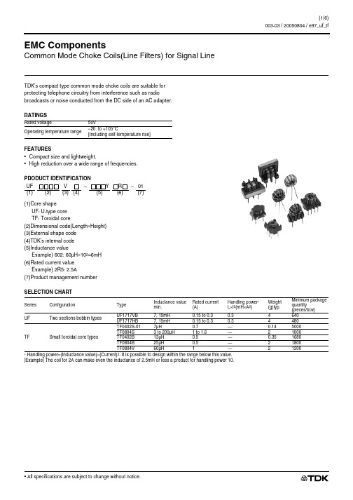
EMC ComponentsCommon Mode Choke Coils(Line Filters) for Signal LineTDK’s compact type common mode choke coils are suitable for protecting telephone circuitry from interference such as radiobroadcasts or noise conducted from the DC side of an AC adapter.RATINGSFEATURES•Compact size and lightweight.•High reduction over a wide range of frequencies.PRODUCT IDENTIFICATION (1)Core shapeUF:U-type core TF:Toroidal core(2)Dimensional code(Length ×Height)(3)External shape code (4)TDK’s internal code (5)Inductance valueExample) 602: 60µH ×102=6mH (6)Rated current value Example) 2R5: 2.5A(7)Product management number SELECTION CHART∗ Handling power=(Inductance value)×(Current)2. It is possible to design within the range below this value.[Example] The coil for 2A can make even the inductance of 2.5mH or less a product for handling power 10.Rated voltage50VOperating temperature range–20 to +105°C[Including self-temperature rise]UF V –Y R –01(1)(2)(3)(4)(5)(6)(7)SeriesConfigurationTypeInductance value min.Rated current (A)Handling power ∗L ×I 2(mH ×A 2)Weight (g)typ.Minimum package quantity (pieces/box)UF Two sections bobbin typesUF1717VB 7, 15mH 0.15 to 0.30.34640UF1717HB 7, 15mH 0.15 to 0.30.34480TF Small toroidal core typesTF0402S-017µH 0.7—0.145000TF0804S 3 to 200µH 1 to 1.6—21000TF0402B 13µH 0.5—0.351680TF0804B 25µH 0.5—21800TF0804V 60µH 1—21200Common Mode Choke Coils(Line Filters) for Signal Line Compact and Separable Bobbin TypeTWO SECTIONS BOBBIN TYPE UF SERIES UF1717VB/UF1717HB TYPESHAPES AND DIMENSIONS/CIRCUIT DIAGRAMTYPICAL ELECTRICAL CHARACTERISTICS IMPEDANCE vs. FREQUENCY CHARACTERISTICSELECTRICAL CHARACTERISTICSPACKAGING QUANTITIESPart No.Inductance (mH)min.DC resistance (Ω)max.Rated current (A)max.UF1717VB-153YR15-011550.15UF1717VB-702Y0R3-017 2.50.3UF1717HB-153YR15-011550.15UF1717HB-702Y0R3-0172.50.3UF1717VB 640pieces/box UF1717HB480pieces/boxCommon Mode Choke Coils(Line Filters) for Signal LineSmall Toroidal Core TypeSMALL TOROIDAL CORE TYPE TF SERIESTF0420S-01 TYPESHAPES AND DIMENSIONS/CIRCUIT DIAGRAM TYPICAL ELECTRICAL CHARACTERISTICSTF0402S-015000pieces/boxCommon Mode Choke Coils(Line Filters) for Signal Line Small Toroidal Core TypeTF0804S TYPESHAPES AND DIMENSIONS/CIRCUIT DIAGRAM TYPICAL ELECTRICAL CHARACTERISTICS IMPEDANCE vs. FREQUENCY CHARACTERISTICSELECTRICAL CHARACTERISTICS∗PACKAGING QUANTITIESPart No.Inductance (µH)min.DC resistance (Ω)max.Rated current (A)max.TF0804S-201Y1R6-012000.0250.7TF0804S-0130.051TF0804S-02600.0361TF0804S1000pieces/boxCommon Mode Choke Coils(Line Filters) for Signal Line Small Toroidal Core TypeTF0402B TYPESHAPES AND DIMENSIONS/CIRCUIT DIAGRAM TF0402B-04P-03TF0402B-05P-01TYPICAL ELECTRICAL CHARACTERISTICSIMPEDANCE vs. FREQUENCY CHARACTERISTICSELECTRICAL CHARACTERISTICSPACKAGING QUANTITIESPart No.Inductance (µH)min.DC resistance (Ω)max.Rated current (A)max.TF0402B-04P-0313450.5TF0402B-05P-0113450.5TF0402B1680pieces/boxCommon Mode Choke Coils(Line Filters) for Signal Line Small Toroidal Core TypeTF0804B TYPESHAPES AND DIMENSIONS/CIRCUIT DIAGRAMTYPICAL ELECTRICAL CHARACTERISTICS IMPEDANCE vs. FREQUENCY CHARACTERISTICSELECTRICAL CHARACTERISTICSPACKAGING QUANTITIESTF0804V TYPESHAPES AND DIMENSIONS/CIRCUIT DIAGRAMTYPICAL ELECTRICAL CHARACTERISTICS IMPEDANCE vs. FREQUENCY CHARACTERISTICSELECTRICAL CHARACTERISTICSPACKAGING QUANTITIESPart No.Inductance (µH)min.DC resistance (Ω)max.Rated current (A)max.TF0804B-08P-01250.10.5TF0804S1000pieces/boxPart No.Inductance (µH)min.DC resistance (Ω)max.Rated current (A)max.TF0804V-04P-02600.0361TF0804V1200pieces/box。
软件体系结构_Lecture5

Alibaba社区开发工程师: 您好,我们对您开发的“全聚德”印象十分深刻, 为此邀请您参与我们最新款的动作冒险游戏《圆桌骑 士》进行设计。您将看到代表游戏角色的类和代表武 器的类,每名角色一次只能使用一种武器,但在
游戏过程中可以切换、买卖、装备、舍弃武器, 您能为我们的架构进行改进么?
performXXX(): public void performFly{ flyBeavior.fly(); } public void performQuack{ quackBehavior.quack(); }
你刚才用到了你的第一个设计模式...
策略模式定义了一系列算法族,并加以封装,让它们之间可以互相
我可以把fly()从超类中取 出来,放进一个 ”Flyable”接口中,只有 会飞的鸭子才实现此接口。 同样的方式,也可以设计 一个”Quackable”,因 为不是每一个鸭子都会叫
如果想改叫声“呱呱”为“吱吱”...
“全聚德”维护团队的反馈 这真是一个超笨的主意,你没 发现这么一来重复的代码会增 多吗?如果你认为覆盖几个方 法不算什么,那么对于48个 Duck的子类都需要稍微修改一 下飞行的行为,你认为如何?!
面向过程设计和面向对象设计 的主要区别是:是否在业务逻 辑层使用冗长的if else判断。 ——《重构》
开放 - 关闭原则: 类应该对扩展开放,对修改关闭。
装饰者模式动态地将职责附加到对象上。对于扩展功能来说,装饰着提供了比继承更有弹性的替代
方案 —— GOF 每个组件都可以单独使用,或者 被装饰者包装起来使用 ConcreteComponent是需要被动 态添加行为的对象,比如饮料
如果牛奶的价格上涨,怎么办? 如果新增一种焦糖风味的调料,怎么办? 某些变态的客人要求两份牛奶外加一份豆浆,怎么办?
基于噪声平衡的抵消共模干扰新技术
Novel Techniques to Cancel Common-mode Noise Based onNoise Balance基于噪声平衡的抵消共模干扰新技术Abstract:概要:Role of winding shielding on the parasitic capacitances of transformer and common-mode (CM) noise is analyzed in details when considering the effects of the secondary side noise source. Based on the proposed model of CM noise, two novel techniques to cancel CM noise by balancing noise is given; experiment results show CM noise is greatly reduced when the techniques are adopted.详细分析线圈屏蔽对变压器寄生电容和共模(CM)噪声的影响。
基于共模噪声模型,俩平衡噪声的新技术用来抵消共模噪声;实验证明共模噪声被显著降低当技术被应用时。
Ⅰ. Introduction一.导言A switching power converter generates larger CM noise as a result of the switching operations in the presence of parasitic capacitance between windings of transformer. In order to reduce common-mode EMI emission, a Faraday shielding between the primary and secondary windings of the transformer is often adopted in practice to reduce the effective coupling capacitance between the windings. Some researches on the modeling of the stray capacitive effects in the transformer were reported [1, 2, 3]. However, they usually did not consider the effects of the shielding and were not good enough for EMI analysis in practical design.变压器绕组间存在技术电容因而开关电源运行时会产生大量的共模噪声。
初步设计模型英语作文

初步设计模型英语作文Title: A Preliminary Design of a Model for English Composition。
Introduction:In the realm of language learning, designing effective models for English composition is paramount. This essay aims to outline a preliminary design for such a model, focusing on key components necessary for comprehensiveskill development.1. Understanding the Purpose:The model begins with a clear understanding of the purpose of English composition. It encompasses various forms such as narrative, descriptive, expository, and persuasive writing. Each form serves different communicative goals and requires distinct strategies.2. Language Proficiency:A fundamental aspect of the model is the development of language proficiency. This includes vocabulary expansion, grammar mastery, and the ability to express ideas fluently and accurately. Providing learners with ample opportunities for reading, writing, listening, and speaking practice is essential.3. Structural Elements:An effective composition model emphasizes the importance of structural elements such as introduction, body paragraphs, and conclusion. Students learn how to organize their ideas coherently, use transition words effectively, and maintain a logical flow of thought throughout their writing.4. Topic Development:Encouraging creativity and critical thinking is central to the model's approach to topic development. Students areprompted to explore diverse subjects, brainstorm ideas, and develop compelling arguments or narratives. This fosters autonomy and cultivates a sense of ownership over their writing.5. Revision and Feedback:Revision and feedback play a crucial role in refining students' writing skills. The model incorporates peer review sessions, teacher feedback, and self-assessment activities. By receiving constructive criticism and engaging in reflective practice, learners enhance their ability to identify and rectify errors.6. Authentic Contexts:To bridge the gap between classroom learning and real-world communication, the model incorporates authentic writing tasks. These may include composing emails, letters, reports, essays, or blog posts on topics relevant to students' interests and experiences. Engaging with authentic materials enhances motivation and fosters adeeper understanding of language use in context.7. Cultural Awareness:An effective English composition model also promotes cultural awareness and sensitivity. Students explore different cultural perspectives through literature, media, and discussions, which enriches their writing with diverse insights and fosters intercultural competence.Conclusion:In conclusion, the preliminary design of a model for English composition outlined above underscores the multifaceted nature of writing proficiency development. By focusing on purpose, language proficiency, structural elements, topic development, revision and feedback, authentic contexts, and cultural awareness, the model seeks to empower learners to become competent and confident writers. Continuous refinement and adaptation based on pedagogical research and student feedback are essential for its efficacy and relevance in language education.。
Line Filter线性滤波器

电气规格: 工作温度:-20°C至+105°C 额定电压:AC250 Vrms最大。 介电强度:5kvac/1分钟。 系列。尺寸: 20系列,24系列, 28,35,42。 联系我们获取更详细的信息。
应用: AC线路滤波器,在彩电产品广 泛应用于,计算机,显示器和 其他电子设备等,广泛应用于 彩色电视机电源,LED显示电 源,电脑开关电源和镇流器。
Line Filter线性滤波器
ET/FT type switch power transformer/ ac line filter ET/FT 类型 开关电源变压器/AC线性滤波器
Features.:特性 Common mode choke (multilayer) capable of high-density mounting 共模扼流圈(多层)可高密度安装 Dual common mode choke coil balun coil/filter双共模扼流线圈线圈巴伦/过滤器 Common mode choke (wire-wound) with low leakage共模扼流圈(绕线式)与低漏 4.7uH to 100mH EMI filter for line filter common-mode choke and EMI coil filter 4.7uH到100MH EMI滤波器线路滤波器共模扼流圈和EMI滤波线圈 Common mode choke used in pulse transformer在脉冲变压器中使用共模扼流圈 Dual wire wound common mode choke coil USB series for signal and noise suppression applications双线绕制的 共模扼流线圈USB系列的信号和噪声抑制的应用 Balun coils/dual wire choke and high-current common mode choke coils 巴伦线圈/双导线电抗器和大电流共模扼流线圈 EMI suppression common mode chokesEMI抑制共模扼流圈 Chokes designed using common-mode choke coil structure to enable better noise suppression 扼流圈使用共模扼流线圈结构,以实现更好的噪声抑制设计的 PFC correction chokePFC校正扼流圈 Current-compensated ring core double chokes电流补偿环芯双扼流圈 Double isolated chokes双隔离电抗器 Current compensated chokes电流补偿扼流圈 Common mode line chokes for high frequency data lines design 共模扼流圈线为高频率的数据线设计 Combination line filter chokes组合线路滤波器电抗器 Power factor controller transformer功率因数控制器变压器 Common mode EMI/RFI filter共模EMI/ RFI滤波器 AC/DC, DC/DC EMI line noise suppressionAC / DC,DC / DC线的EMI噪声抑制 Communication system EMI line noise suppression通信系统的EMI线路噪声抑制 Automotive system EMI line noise suppression汽车电子系统EMI线路噪声抑制 LCD/PDPT television EMI line noise suppression液晶/ PDPT电视线的EMI噪声抑制 Computer peripheral equipment EMI line noise suppression 电脑周边设备的EMI线路噪声抑制系统的通信线路的EMI噪声抑制
毕业设计论文外文文献翻译模块化设计:产品设计的分解与整合中英文对照#(精选.)

英文原文:Design for Modularity: Product Design for Decomposition and IntegrationABSTRACTIn the last few years, corporation has engaged in studies to improve their design processes, ranging from marketing to support. Recent government, academic and industrial sector initiatives have sought advance technologies for developing and managing product development environment. Many companies have established a concurrent design process for their product development and have recognized a need for tools in evaluating the level of decomposition and integration, while analyzing the impact on the final design. This article will propose a three-phase methodology for design of products while considering modularity, assembly and manufacture.KEYWORDSModularity, Group technology, Optimization, Decomposition, Classification1. IntroductionModular design is a design technique that can be used to develop complex products using similar components . Components used in a modular product must have features thatenable them to be coupled together to form a complex product. Modular design can be also viewed as the process of producing units that perform discrete functions, and then the units are connected together to provide a variety of functions. Modular design emphasizes the minimization of interactions between components, which will enable components to be designed and produced independently from each other. Each component, designed for modularity, is supposed to support one or more function. When components are structured together, to form a product, they will support a larger or general function. This shows the importance of analyzing the product function and decomposing it into sub-functions that can be satisfied by different functional modules. Modularity can be applied in the product design, design problems, production systems, or all three. It is preferable to use the modular design in all three types at the same time.Modular products refer to products that fulfill various overall functions through the combination of distinct building blocks or modules. In the sense that the overall function, performed by the product, can be divided into sub functions that can be implemented by different modules or components. An important aspect of modular products is the creation of a basic core unit to which different elements (modules) can be fitted, thus enabling a variety of versions of the same module to be produced. The core should have sufficient capacity to cope with all expected variations in performance and usage.Most design problems can be broken down into a set of easy to manage simpler sub-problems. Sometimes complex problems are reduced into easier sub-problems, where a small change in the solution of one sub-problem can lead to a change in other sub-problems’ solutions. This means that the decomposition has resulted in functionally dependent sub-problems. Modularity focuses on decomposing the overall problem into functionally independent sub-problems, in which interaction or interdependence betweensub-problems is minimized. Thus, a change in the solution of one problem may lead to a minor modification in other problems, or it may have no effect on other sub-problems.Modularity in production systems aims at building production systems from standardized modular machines. The fact that a wide diversity of production requirements exists has led to the introduction of a variety of production machinery, and a lack of agreement on what the building blocks should be. This means that there are no standards for modular machinery. In order to build a modular production system, production machinery must be classified into functional groups from which a selection of a modular production system can be made to respond to different production requirements. Rogers classified production machinery into four basic groups of “primitive” production elements. These are process machine primitives, motion units, modular fixtures, and configurable control units. It is argued that if a selection is made from these four categories, it will be possible to build a diverse range of efficient, automated and integrated production system.2.Overview of Product DevelopmentProduct development is a necessary and important part of the activities performed by a manufacturing firm. Due to changes in manufacturing technology, consumer preferences, and government regulations (to name a few influences), existing products will become less profitable over time. The sales volume of a typical product starts slowly, accelerates, becomes flat, and then steadily declines. Although there may be a few products that remain profitable for many years, firms continually develop new products that will generate more profits. Product development determines what the firm will manufacture and sell. That is, itattempts to design products that customers will buy and to design manufacturing processes that meet customer demand profitably. Poor decisions during product development lead to products that no one wants to buy and products that are expensive to manufacture in sufficient quantity.A product development process is the set of activities needed to bring a new product to market. A product development organization includes the engineers, managers, and other personnel who make process and product engineering decisions and perform these activities. (Note that, in this paper, the term new product covers the redesign of an existing product as well.)Because making good decisions requires expertise and an organization of people can be experts in only a few things, a manufacturing firm specializes in a certain class of products. It focuses its attention on the market for that class of products, the technologies available to produce that class, and the regulations relevant to that class.Like other parts of the business, a product development organization seeks to maximize the profit of the manufacturing firm subject to the relevant regulatory and ethical constraints and other conditions that the firm’s owners impose based on their values. A product development organization does this by regularly introducing new products that the firm can manufacture, market, and sell. Fundamentally, then, a product development organization transforms information about the world (e.g., technology, preferences, and regulations) into information about products and processes that will generate profits for the firm. It performs this transformation through decision-making (Herrmann and Schmidt, 2002). Because the design problem is highly complex, product development teamsdecompose the problem into a product development process, which provides the mechanisms for linking a series of design decisions that do not explicitly consider profit.The following nine steps are the primary activities that many product development processes accomplish (Schmidt et al., 2002):Step 1. Identify the customer needs.Step 2. Establish the product specification.Step 3. Define alternative concepts for a design that meets the specification.Step 4. Select the most suitable concept.Step 5. Design the subsystems and integrate them.Step 6. Build and test a prototype; modify the design as required.Step 7. Design and build the tooling for production.Step 8. Produce and distribute the product.Step 9. Track the product during its life cycle to determine its strengths and weaknesses.This list (or any other description that uses a different number of steps) is an extremely simple depiction that not only conveys the scope of the process but also highlights the inherent (but unquestioned) decomposition. There are many other ways to represent product development processes and the component tasks, including the use of schedules or a design structure matrix (Smith and Eppinger, 2001).Manufacturing firms understand that design decisions (though made early in the product life cycle) have an excessive impact on the profitability of a product over its entire life cycle. Consequently, product development organizations have created and used concurrent engineering practices for many years (Smith, 1997, provides a historical view). Many types of tools and methods (such as cross-functional product development teams and design for manufacturing guidelines) have been created, adopted, and implemented to improve decision-making. Cooper (1994) identifies three generations of formal approaches to product development, all of which involve decomposition.It should be noted, however, that decomposition is not the only way to describe product development. As an alternative to decomposing a system design problem into subproblems, Hazelrigg (1996) proposes creating and refining system design models to express how detailed design variables affect the overall system performance. Thisapproach suggests that a product development process would end with using the model to find the optimal design. Hazelrigg (1998) encourages this type of optimization but does not discuss the process of generating the profit maximization model.3. A Methodology for Design for ModularityA three-phase methodology is proposed for the development of complex products using the modularity concept [1,2]. The proposed methodology matches the criteria set by the design for functionality, assembly and manufacture. Some of the major benefits associated with this methodology include:·Increased design accuracy, efficiency, and the reuse of existing design for new programs.·Potential for integration of the developed methodology and technology into the engineering design activities.·Modular product design and the process of planning the production are integrated in one overall engineering process in which product features are mapped into their feasible process(es) in a one to one correspondence.In order to implement this concept successfully, the manner in which the modules are selected is critical. By establishing simple interfaces within the modules, the numbers of interactions are then reduced. The steps associated with this methodology include:Phase I - Decomposition Analysis: Design for Modularity and Classification1. Product and problem decomposition.2. Structural and modular decomposition.3. Associativity analysis between the components and specification.4. Application of group technology classification system.5. Construction of the associativity measure matrix.6. Optimum selection of modules.Phase II - Product Analysis: Design for Assembly and Functionality Analysis1. Identify the components that could be produced and assembled separately.2. Determine of the order of disassembly and assembly for each sub-component module.3. Establish the interfaces based on the analysis of the design features.4. Determine of the order, which the sub-assemblies are assembled to produce the final product.Phase III - Process Analysis: Design for Manufacture1. Family identification and template retrieval.2. Determination of the logical order of GT codes for the process of modules.3. Machine and process parameter calculation.4. Variant process planning.4. Decomposition Analysis: Design for Modularity and ClassificationPhase I of the methodology further specifications associated with this phase are illustrated as follows:4.1. Needs AnalysisThe design engineer is usually given an ill-defined problem. In many situations, the designer has to respond to the mere suggestion that there is a need for a product to perform a certain function. One of the main tasks is to find out precisely what are the needs and what do customers really want. An important step in the design is to describe the product fully in terms of functional needs and physical limitations. These functional needs and physical limitations will form the product specifications. Surveying prospective purchasers or customers could collect information required to identify customer needs. Conducting a marketing study that begins by establishing target markets and customers can do this. Then customers’ wants and needs could be obtained by using several methods such as interviews and questionnaires. Also, similar products (competitive products) are investigated to find possible improvement opportunities by focusing on weakness points and desired features by customers. Next, customer wants and needs are arranged into groups and prioritized according to their importance. Needs analysis usually results in a statement of recognized needs and the expected manner in which that need should be met.4.2. Product Requirements AnalysisResults of the needs analysis step are used to identify the product requirements. The development group begins by preparing a list of functional objectives needed to meet the customer’s primary needs. Further analysis of customer needs reveals operational functional requirements that impose both functional and physical constraints on the design. Secondary customer requirements will be categorized as general functional requirements; they are ranked secondary because they will not affect the main function of the product. That is, a product may lack one or more general functional requirement and still be considered as a functional product that meets the intended function. General functionalrequirements should be weighted with respect to their importance.4.3. Product Concept AnalysisProduct/concept analysis is the decomposition of the product into its basic functional and physical elements. These elements must be capable of achieving the product’s functions. Functional elements are defined as the individual operations and transformations that contribute to the overall performance of the product. Physical elements are defined as the parts, components, and subassemblies that ultimately implement the product’s function. Product concept analysis consists of product physical decomposition and product functional decomposition. In product physical decomposition, the product is decomposed into its basic physical components which, when assembled together, will accomplish the product function. Physical decomposition should result in the identification of basic components that must be designed or selected to perform the product function. Product functional decomposition describes the products overall functions and identifies components functions. Also, the interfaces between functional components are identified.4.4. Product/Concept IntegrationBasic components resulting from the decomposition process should be arranged in modules and integrated into a functional system. The manner by which components are arranged in modules will affect the product design. The resulting modules can be used to structure the development teams needed. System level specifications are the oneto- one relationship between components with respect to their functional and physical characteristics. Functional characteristics are a result of the operations and transformations that components perform in order to contribute to the overall performance of the product. Physical characteristics are a result of the components’ arrangements,assemblies, andgeometry that implement the product function. Physical and functional characteristics, forming the system level specifications, are arranged into a hierarchy of descriptions that begins by the component at the top level and ends with the detailed descriptions at the bottom level.Bottom level descriptions (detailed descriptions) are used to determine the relationships between components, 1 if the relationship exists and 0 otherwise. This binary relationship between components is arranged in a vector form, “System Level Specifications Vector”(SLSV). System leve l specifications identified in the previous step affects the general functional requirements in the sense that some specifications may help satisfy some general functional requirements, while other specifications might prevent the implementation of some desired general functional requirements. The impact of the SLS on GFR’s should be clearly identified which will help in developing products that will meet, up to a satisfactory degree, the general functional requirements stated earlier. The impact will be determined based on –1 as negative impact, 0 as no impact, and 1 as positive impact. A negative impact represents an undesired effect on the general functional requirements such as limiting the degree to which the product will meet the general requirement, or preventing the product from implementing the general requirement. While a positive impact represents a desired effect that the SLS will have on the general requirements, such SLS will ensure that the product will satisfy the requirements and result in customer satisfaction. An SLS is said to have no impact if it neither prevents the implementation of the GFR, nor helps satisfying the GFR.The degree of association between components should be measured and used in grouping components into modules. Incorporating the general functional requirement weights can do this, in addition to the system level specifications vectors and their impactson the general functional requirements to provide a similarity index between components.The similarity indices associated with components are arranged in a component vs. component matrix. Components with high degree of association should be grouped together in design modules. This can be accomplished by using an optimization model that maximizes the sum of the similarities. The optimization model will identify independent modules that can be designed simultaneously. Several models are available for optimization analysis of this model.5.Types of DecompositionA product development process follows a decomposition scheme that reflects the experience of the organization and the individuals that inhabit the organization. This relationship explains the design of many organizations and business processes, of course, and obviously applies to product development processes as performed in the real-world. (The study of contingency theory has explored the relationship of organization structure to the organization’s goals and environment.) The evolution of the product development process is influenced by exceptional events (such as disasters that cause managers to implement controls or regulations designed to ensure that “it never happens again”), by executives and managers who participated in or observed different processes used by other organizations, and by natural processes of continuous improvement. These influences are resisted by the inertia of individuals in the organization (“that’s not the way we do it here”), and the implemention of innovations may fail for other reasons. Klein and Sorra (1996) argue that the implementation effectiveness depends upon implementation climate and implementation policies and practices.Holt et al. (1960) mention a three-stage process for the evolution of a decision-making system. In the first stage, when an organization is small, skilled managers make decisions as situations arise. In the second stage, the complexity of the operations increases, and the firm installs a system of decisionmaking. For routine decisions, heuristics or simple rules guide decision-making. In the third stage, the firm seeks to improve decision-making by implementing decision support tools. Often these tools help decision-makers treat problems in a more integrated fashion.In conclusion, rarely are product development processes explicitly designed to optimize profitability. Still, the never-ending quest to improve processes leads managers to change them, first hoping to improve this metric, then hoping to improve another, always seeking changes that improve all metrics simultaneously. Because different firms find themselves in different positions, they seek different things from their processes. More precisely, there exist a large set of objectives, and each organization prioritizes these objectives differently. Thus, each firm finds a different process most desirable for itself, in the same way that different families looking at the houses for sale in the same city choose different houses based on their own priorities on location, price, number of bedrooms, and so forth.Being unique, each product development organization has a unique product development process that embodies a unique decomposition. If each process has changed over time due to many different reasons, it may seem unreasonable to describe the forces that shape specific product development processes. Indeed, Blanchard and Fabrycky (1998) state that a development process is a generic template that must be “tailored” to a specificproject’s need. They describe three common processes: the waterfall model,the spiral model, and the V model. They observe that preferences among these models are subjective and that careful study is needed to select the best model for a specific project.Still, some authors have described some of the factors that make certain types of processes more or less successful. For instance, Loch and Terwiesch (1998) use an analytical model of concurrent engineering to show how uncertainty (and the speed of uncertainty reduction) affects the optimal amount to overlap activities and the optimal frequency of meetings used to coordinate the concurrent activities. More generally, Pich, Loch, and De Meyer (2002) identify three project management strategies (instructionism, learning, and selectionism) that handle uncertainty in different ways. Accordingly, project managers must determine the adequacy of what is known about the world and the effects of different actions and must determine whether any inadequacy is due to ambiguity or complexity. The paper proposes some simple rules suggesting when to use each strategy.6. Summary and ConclusionsThis article has presented a new methodology for modular design. The complete process is a three-phase process, but only phase I of the methodology is presented. The method illustrates the significance of the group technology coding and classification and the optimization in modular design.This synthesis contributes to a theory of design describes how design happens in practice and explains this behavior. The fundamental axioms include the profitmaximization objective, bounded rationality (including limited time and resources available for product development), and the presence of uncertainty.Extending this theory of design will require better understanding of the advantages and drawbacks of different decompositions. Also useful will be understanding the relationship between the effort spent to solve a design subproblem and the quality of the resulting solution.It will be interesting to see how improvements in information technology and decision support systems increase the amount of information that one decision-maker can process and how these improvements change the balance between decomposition and integration.中文翻译:模块化设计:产品设计的分解与整合摘要:在过去的几年里,公司进行了研究,以改善他们的设计流程,从市场营销支持。
- 1、下载文档前请自行甄别文档内容的完整性,平台不提供额外的编辑、内容补充、找答案等附加服务。
- 2、"仅部分预览"的文档,不可在线预览部分如存在完整性等问题,可反馈申请退款(可完整预览的文档不适用该条件!)。
- 3、如文档侵犯您的权益,请联系客服反馈,我们会尽快为您处理(人工客服工作时间:9:00-18:30)。
Simplified Design of Common-Mode Chokes for Reduction of Motor Ground Currents in InverterDrivesA.MuetzeC.R.SullivanFound in IEEE Industry Applications Society Annual Meeting,Oct. 2006,pp.2304–2311.c 2006IEEE.Personal use of this material is permitted.However,permission to reprint or republish this material for advertising or promotional purposes or for creating new collective works for resale or redistribution to servers or lists, or to reuse any copyrighted component of this work in other works must be obtained from the IEEE.Simplified Design of Common-Mode Chokes for Reduction of Motor GroundCurrents in Inverter DrivesAnnette Muetze Charles R.SullivanDept.of Electrical and Computer Engineering Thayer School of Engineering University of Wisconsin–Madison,Madison,WI53706USA Dartmouth College,Hanover,NH03755USA muetze@ chrs@ Abstract—A simplified design calculation for common-mode chokes for reducing motor ground currents provides insight on the effects of various parameters and allows easy design.Key simplifying assumptions are that the voltage rise time is short compared to the ring period and that the damping is small.Example designs for machines up to450mm frame size show how effective ground-current reduction is possible with small,inexpensive,single-turn chokes.I.I NTRODUCTIONThe high-frequency(HF)ground current that can occur in inverter-based drive systems can cause different parasitic phe-nomena.Depending on the overall system,notably the drive size and presence of additional mitigation techniques,these parasitic phenomena can lead to early drive failure due to HF circulating bearing currents and bearing currents due to rotor ground currents,wide band EMI,and interference with ground fault protection systems in industrial facilities,to name some[1]–[9].Common-mode chokes that are placed in the inverter-output (Fig.1)can be a cost-effective method of reducing such ground currents in motors used with PWM drive systems[4],[6]–[8]. Because of the interaction between the circuit waveforms,the choke value,the possible use of the motor-inverter interconnect cables,and the large current magnitude,the requirements for such chokes differ from standard choke design[10].Because of the large size of the motor leads of higher-power drives,feed-through chokes with only one turn are more easily installed than wound chokes.More complicated structures,such asfilter s that provide a connection to the inverter-dc link,are beyond the scope of this contribution.II.D ESIGN A PPROACH:S IMPLIFYING A SSUMPTIONS We model the circuit as a simple series LRC circuit(similar to what is done in[4],[6])with an input that ramps rapidly from one constant voltage to another,at each switching transition.Each switching transition is analyzed independently.This approach is justified as the ring period is long compared to the transition time,MotorInverterCommonmodechokeFig.1.Simplified sketch to illustrate placement of common mode choke in the inverter-output.particularly with large drives and with effectively used common-mode chokes[10].If the ring period is long compared to the transition time,the slope dv/dt has little bearing on the ground current,and we can simplify the analysis by assuming an instantaneous step in the input voltage(infinite dv/dt).Although the assumption of a short transition time is not always accurate in practice,it can be a useful simplifying assumption which facilitates analytical design equations which give general guidance to designers.We proceed with design using this assumption.Simulation results in Section V confirm that the error introduced is small.The analysis also depends on the resistance value and the degree of damping.As the inductance is increased,the damping is decreased,assuming the losses in the inductor itself are small.Thus,we are typically interested in low-damping cases. Exemplarily,Fig.2shows the dependency of the peak current on the inductance value for different capacitance values dv/dt= 2kV/µs,and R=1Ω(simulation results).As the low-damping case is also the worst-case situation,it is reasonable to limit the analysis to this situation.With the assumptions of a common-mode step input of ampli-tude∆V and light damping,a design that does not saturate will limit the peak ground current(common-mode)to approximatelyI peak≈∆V/L/C(1) Although this simplified analysis will not hold for all designs,it will hold for the designs we wish to choose,so we can proceed with the choke design based on(1).10203040506070801.E-12 1.E-10 1.E-08 1.E-06 1.E-04 1.E-02 1.E+00Simulated peak HF ground current[A]Common mode inductance[H] Fig.2.Dependency of peak current on inductance values,for different capaci-tance values dv/dt=2kV/µs,R=1Ω.III.C HOKE D ESIGNWe proceed to design a choke based on(1).The choke must achieve the required inductance:L=∆VI peak2C(2)which we equate to the inductance for a given core geometryL=N2µA cc=∆VI peak2C(3)where c is the circumferential length,A c the cross sectional area (Fig.3),µthe permeability,and N the number of turns.Note that A c=ab is the cross sectional area that can be given by any aspect ratio a:b.lFig.3.Toroid nomenclature.We now have a specification for the inductance and a spec-ification for the peak current,which is sufficient information to use with any standard inductor design procedure.However, proceeding with the analysis of this particular case is important for two reasons.1)We wish to develop equations that directly show how theparameters of the application,∆V,C,and I peak,affect the inductor design.2)The inductor may be wound with the cable used to connectthe inverter to the motor,which changes the design consid-erations relative to those for a typical inductor wound from wire chosen for the inductor.In this case,the wire diameter isfix ed,and it is also desirable to use only a single turn. The next step in completing an inductor design is to consider flux density,which may in general be limited by saturation or by core loss.Since the common-mode currents are in the form of short spikes,we assume that saturation,rather than core loss,is the relevant constraint.This constraint can be examined through a direct calculation of the peakflux density,or by considering energy storage.Either leads to the same results;we choose to consider energy.The core may or may not be gapped,but we unify the treatment by considering gapped cores in terms of an effective permeabilityµeff=µ.Equating the required energy storage to the actual energy storage results in1 2LI2peak=12B peak Hdv.(4)Assuming uniformflux density throughout the core,and linear magnetics,we haveLI2peak=B2peakµA c c.(5)Solving for the volume(approximated by A c c)and using(3)we obtainA c c=Cµ(∆V)2B2peak.(6)Although(6)is an appealingly simple equation,it is potentially misleading—it might seem to indicate that the use of low permeability would enable the use of arbitrarily small volume cores.However,such a design would need to have a very small window area,and the requiredfine wire would have excessive resistance and would overheat.(In the limit,the design would be a short length of ultrafine wire which has high inductance per unit length,but very little current carrying capability.)Thus,we must also consider the window area available for the winding,which,for a circular window of a toroidal core,is A w=πr2,where r is the window radius.As we are seeking to develop design equations that give general guidance to designers we are simplifying2πr≈ c thus r≈ c/(2π),where the error introduced will depend on how the cross sectional area A c=ab is being realized.Then,A w≈2c4π=µ2N2I2peak4πB2peak(7)which directly shows that a small permeabilityµwill require a vanishingly small window area to meet the specifications. Assuming we have control of the permeability value(either through selection of the core or gapping),a smaller window size is desirable insofar as it is feasible.So it is necessary to establish a minimum window size to proceed with the design.This depends on the wire used to wind the choke and the number of turns. The simplest option is to wind the choke with the same wires used to connect the inverter to the machine,and we consider this casefirst.Note also that the approach includes both multi-turn wound chokes and the more easily installed single-turn feed-through chokes.A.Case1:Fixed wire diameter;free choice ofµConsider winding the choke with the machine lead wire con-necting the inverter to the machine,which has outside diameter d o,including insulation,per-phase.The required window area is, for three phase wires,A w=3πNd2o4F p(8)where F p is a packing factor,defined as ratio of the wire area (including insulation)to the core window area.For a circular window,the maximum packing factor can be calculated fromsimple geometrical considerations to beF p,max=3π(d o/2)2A w=3π(d o/2)2π(d o/2)2(1+1/(√3/2))2=9(√3+2)2≈0.646.(9)From(7)and(8),we obtain2c 4π=3πNd2o4F p(10)c=πd o3F p√N(11)We define a constant k w=πd o3F pto enable writing this moresimply asc=k w √N.(12)This result can be used with(12)to establishµ=k wB peak√NI peak.(13)Using this value of permeability in(6),we obtain an expression for magnetic volume:A c c=(∆V)2B peakCI peakk w√N(14)or,writing out k w explicitly,A c c=(∆V)2B peakCI peakπd o3F p1√N.(15)The core size as expressed by either(14)or(15)appears dramatically different from standard inductor sizing equations, which typically show the size as proportional to LI2,with a fix ed temperature rise(the Hanna-curve method[11])or afix ed Q value(the K g method[12]).The dependence on L in(14) and(15)is hidden,instead,the result is written in terms of the performance and application specifications.The dependence on current is different because it is assumed that I peak is in effect for a short enough time that the winding dissipation associated with it is insignificant.Based on the above analysis,we can completely specify thedesign withc=πd o3F p√(16)A c=(∆V)2B peakCI peak1N(17)µideal=πd o3F p√NI peak B peak(18)From these equations we can draw several conclusions:•A high packing factor is preferred;i.e.,for a given wire diameter,one should ordinarily use the minimum core window size that the wire willfit through.The core size is reduced by a high packing factor(15),as is the required permeability.An exception to this rule is if the permeability found from(18)was lower than available permeabilities, and gapping was not practical.This situation is addressed in Section III-C.However,if the ideal permeabilityµideal found from(18)is higher than is available,as discussed in Section III-B,a high packing factor is still preferred.•In contrast to a standard inductor design,in which the re-quired effective permeability is inversely proportional to the number of turns,the required effective permeability based on our constraints and assumptions decrease more slowly as the number of turns increases,inversely proportional to the square root of N.Because there is less benefit from an increased number of turns,we can expect small numbers of turns to work well here more often than they do in standard chokes.The core volume also decreases slowly with increased N;it is also inversely proportional to the square root of N.B.Case2:Fixed wire diameter;ideal permeabilityµideal higher than available permeabilityµaIf the available permeability is smaller than would be ideal, the inductor is not saturated,and the core area is chosen simply to meet the inductance specifications with the given permeability. Solving(3)for core area,and applying the calculation of length from Case1(12),we obtain the required core areaA c=C∆V2I2peakk wN32µa(19) and the required core volumeA c c=C∆V2I2peakk2wNµa.(20)In this case,the volume decreases faster than in Case1as the number of turns is increased(inversely proportional to N), which makes increasing N a more appealing strategy than it is in Case1.This applies until saturation is reached,at which point the design reverts to Case1,and crosses over to having the ideal permeabilityµideal lower than the available permeability µa(Case3discussed below in Section III-C),at which point no further reduction in core volume is possible by increasing the number of turns.Thus we expect that in some designs,a good choice will be at the border between the cases,i.e.,with the number of turns that results in(18)giving the highest available value of permeability.However,a better choice in most cases will be to simply use one turn made by passing the motor leads through the core.Since these leads have a large outer diameter d o,increasing the choke volume is preferable to using multiple turns in terms of ease of handling.Furthermore,considering the additional length of the wire(N−1) t over the length with no choke,where t is the length of one turn,also demonstrates the advantage of single-turn designs.TABLE IE XAMPLE D ESIGNS FOR C ASE1:F REE C HOICE OF P ERMEABILITY,N=1Frame size∆V C Leads/phase d o I cm,peak L V olume A c c c A cµideal/µ0Ring frequency mm V nF mm AµH cm3cm cm2kHz31518712116516.78.612.30.72351535540018720130107.013.423.10.62204542640018720223107.014.324.60.6235294264501872523015 3.915.632.10.52046051131532212110549.816.07.7 2.114697206400322201231020.730.617.7 1.716901247400322202161020.729.617.1 1.716368247450322252231511.535.524.6 1.415686297 C.Case3:Fixed wire diameter;ideal permeabilityµideal lowerthan available permeabilityµaIf the available permeabilityµa is larger than the idealpermeability calculated by(18),in principle,it is possible togap the core and achieve an effective permeability equal to theideal permeability.However,if the difference between the idealpermeability and the available permeability is small,the idealgap would be smaller than might feasible,and would be unlikelyto be worth the added expense.Thus,it is also of interest toconsider design with afix ed permeability larger than ideal.Thevolume of such a design is given by(6),as for designs using theideal permeability.However,the result is now a constant volume,independent of the number of turns,since the permeability isfix ed.Thus,there is no reason to increase the number of turns.To complete the design byfinding core path length and area,we start by noting in(6)that an increase in permeability requiresa proportional increase in volume.Starting with the design basedon the ideal permeability,with length specified by(16)and areaspecified by(17),we need to decide how to allocate this increasein volume between length and area.Since an inductor built witha core of permeabilityµa has inductanceL=N2µa A cc(21)an increase of c by a factorµa/µideal while also increasingµwill maintain the original inductance value,whereas increasing A c by the same factor as the increase inµwill increase the inductance by the square of the permeability ratio(µa/µideal)2. If the permeability is trulyfix ed at a constantµa,the higher inductance solution(increased A c)would be preferred,because it further decreases ground current.However,if the permeability is a strong function of frequency,the increased inductance that results from using a larger A c decreases the ring frequency,which further increases the permeability,which in turn further increases the required volume.Thus,with frequency-dependent permeability,the minimum-volume design uses the same area as the ideal-permeability design,as specified by(17),and uses a lengthc=µaµidealc,µideal=Nµa I peak B peak(22)as can be seen by substitution using(18)and(16),or from directly applying Ampere’s law.D.Case4:Variable wire sizeIn the case that the inductor is not wound with the same wire used to for connection between the inverter and the machine,the wire diameter and number of turns may be selected specifically for the inductor.Once the inductance requirement is found from (2),the design becomes similar to standard inductor design for other applications,as described in many textbooks.IV.E XAMPLE D ESIGNSA.Drive parameters for example designsWe consider8different example cases based on typical val-ues for three-phase machines with random-wound winding.The machines have315,400,and450mm frame size.Both voltage ratings400V and690V are considered.Machine supply via one motor lead per phase is assumed for the smallest,two motor leads per phase for the largest,and both case for the400mm frame size machine.These parameters along with the corresponding values of the operating dc bus voltage V dc,the common-mode voltage step∆V(obtained by averaging the three phases when one phase makes a transition),d o,and typical values for C are summarized in Table II.We take B peak equal to the saturationflux density of typical nanocrystalline material at1.2T,packing factor F p=0.5for one and F p=0.25for two machine lead per phase,and we attempt to limit peak ground current to5A(peak-to-peak of10A),10 A,and15A for the three machine sizes respectively.B.Design with free choice of permeabilityµThe result for a single turn design for the315mm400V machine is L=16.7µH(from(2)),volume of8.6cm3(from (15)),relative permeabilityµ/µ0=23515(from(18)),pathTABLE IID RIVE P ARAMETERS FOR E XAMPLE D ESIGNSFrame size V oltage rating V dc∆V Leads/phase d o C mm V V V mm nF3154005601871161240040056018713020400400560187223204504005601872302531569096632211012400690966322123204006909663222162045069096632222325length of 12.3cm (from (16)),core area of 0.7cm 2(from (17)),and a ring frequency of 355kHz (from L and C ).These values,along with the corresponding values for the other seven example cases,are listed in Table I.At a voltage transition slope of 2kV/µs,the rise time for V dc =560V is 0.28µs,which is less than two thirds of a period for all three frame sizes.This indicates that the instantaneous rise assumption is reasonably good,as is further confirmed by simulation below (Section V).C.Design based on an available permeability of 10000µ0Although both amorphous and nanocrystalline cores are avail-able with nominal relative permeabilities of 80000or more their relative permeability is typically in the range of 10000to 20000in the range of 200to 500kHz [13]–[16].The designs in Table I require permeabilities in this neighborhood,but often higher than what is available.Thus we need to consider Case 2,in which the available permeability µa is smaller than would be ideal.We first consider a conservative assumption of an available permeability of µa =10000µ0.From (19)and (20),we can calculate the required area and volume as a function of the number of turns,as shown in Table III.Although the core volume decreases significantly for large numbers of turns (∝1/N )(Fig.4),the wire volume and difficulty of winding go up greatly for numbers of turns greater than one.Thus single-turn designs are still likely to be the most practical choice.If necessary,the larger core needed for a single turn can be assembled from several smaller cores stacked in series.Since the ideal permeability is also a function of the number of turns (18),the assumed permeability of 10000is higher than ideal for some designs in Table III,as marked with *in the table.The parameters for these designs are calculated as described in Section III-C.Note that once this point is reached,the core volume is independent of the number of turns,and so increasing the number of turns further offers no advantage.102030405060315m m ,400V ,1l e a d /p h a s e400m m ,400V ,1l e a d /p h a s e400m m ,400V ,2l e a d s /p h a s e450m m ,400V ,2l e a d s /p h a s e315m m ,690V ,1l e a d /p h a s e400m m ,690V ,1l e a d /p h a s e400m m ,690V ,2l e a d s /p h a s e450m m ,690V ,2l e a d s /p h a s el 3Fig. 4.Core volume A c c for different numbers of turns and available permeability of 10000µ0(Table III).Most entries are calculated based on case 2:ideal µideal higher than available µa ;the entry marked with *has an ideal permeability below 10000µ0and is calculated based on case 3:ideal µideal lower than available µa .TABLE IIIE XAMPLE D ESIGNS FORC ASE 2:P ERMEABILITY OF 10000µ0(CONSERVATIVE ASSUMPTION ).M OST ENTRIES ARE CALCULATED BASED ON CASE 2:IDEAL µideal HIGHER THAN AVAILABLE µa ;THE ENTRIES MARKED WITH *HAVE IDEAL PERMEABILITY BELOW 10000µ0AND ARE CALCULATEDBASED ON CASE 3:IDEAL µideal LOWER THAN AVAILABLE µa .315mm,400V ,1lead/phase,C =12nF,L =16.7µH,d o =16mmNumber of turns,N 12345Core area,A c ,cm 21.640.580.320.210.15Circumferential length, c ,cm 12.317.421.324.627.5Core volume,A c c ,cm 320.210.1 6.73 5.04 4.04400mm,400V ,1lead/phase,C =20nF,L =7.0µH,d o =30mm Number of turns,N 12345Core area,A c ,cm 21.280.450.250.160.12Circumferential length, c ,cm 23.132.640.046.251.6Core volume,A c c ,cm 329.614.89.857.39 5.9400mm,400V ,2leads/phase,C =20nF,L =7.0µH,d o =23mm Number of turns,N 12345Core area,A c ,cm 21.370.480.260.170.12Circumferential length, c ,cm 24.634.942.749.355.1Core volume,A c c ,cm 333.716.811.28.49.7450mm,400V ,2leads/phase,C =25nF,L =3.9µH,d o =30mm Number of turns,N 12345Core area,A c ,cm 20.990.350.190.120.10*Circumferential length, c ,cm 32.145.555.764.378.5*Core volume,A c c ,cm 331.815.910.68.07.6*315mm,690V ,1lead/phase,C =12nF,L =49.8µH,d o =10mm Number of turns,N 12345Core area,A c ,cm 2 3.05 1.080.69*0.52*0.42*Circumferential length, c ,cm 7.710.915.7*20.9*26.2*Core volume,A c c ,cm 323.511.710.9*10.9*10.9*400mm,690V ,1lead/phase,C =20nF,L =20.7µH,d o =23mm Number of turns,N 12345Core area,A c ,cm 22.92 1.030.560.43*0.35*Circumferential length, c ,cm 17.725.030.741.9*52.4*Core volume,A c c ,cm 351.725.917.218.1*18.1*400mm,690V ,2leads/phase,C =20nF,L =20.7µH,d o =16mmNumber of turns,N 12345Core area,A c ,cm 2 2.831.000.540.43*0.35*Circumferential length, c ,cm 48.524.229.741.9*52.4*Core volume,A c c ,cm 317.124.216.218.1*18.1*450mm,690V ,2leads/phase,C =25nF,L =11.5µH,d o =23mm Number of turns,N 12345Core area,A c ,cm 2 2.260.800.430.36*0.29*Circumferential length, c ,cm 24.634.842.762.8*78.5*Core volume,A c c ,cm 332.127.818.622.6*22.6*D.Design based on the permeability available at the calculated ring frequencyGiven sufficiently accurate data on the permeability as a function of frequency,such as that published in [15],it is possible to do more precise design work,basing each design on the permeability available at the calculated ring frequency listed in Table I.The curves in [15]are remarkably similar for amorphous or nanocrystalline materials in the frequency range of interest,consistent with the general trends in other references [13]–[16].Depending on whether the available permeability is higher orTABLE IVE XAMPLE D ESIGNS FOR P ERMEABILITY A VAILABLE AT THE C ALCULATED R INGF REQUENCY ,N =1Frame size ∆V C Leads/phased o I cm,peakL V olume c A c µa /µ0Ring frequencymm V nF mm A µH cm 3cm cm 2kHz 31518712116516.712.612.3 1.01597535540018720130107.020.323.10.91452942640018720223107.023.224.60.9145294264501872523015 3.924.232.10.81317251131532212110549.822.510.9 2.120755206400322201231020.734.520.0 1.719089247400322202161020.734.520.0 1.719089247450322252231511.539.627.51.417488297lower than the ideal permeability,the design calculations may be based on the equations in Section III-B or Section III-C.Here,only single-turns are considered because of the reasoning given previously in Section IV-C and to avoid an overflo w of data.These results are shown in Table IV.Note that regardless of whether the permeability is too high or too low,the core volume ends up larger than that in the initial designs in Table I.E.Discussion of the design resultsFig.5illustrates the results for the core volumes for the three designs.The figures illustrate well that:•The smallest core volumes result from the use of the ideal permeability.•Regardless of whether the available permeability is higher or lower than the ideal one,the core volume with the available relative permeability (Table IV)ends up larger than that in the initial design (Table I).•The core path length c is identical for many sets of designs because it is chosen as the smallest possible to fit the wire used.The designs with longer path lengths are those in which the available permeability is higher than ideal,and the path length is increased to avoid saturation.102030405060315m m ,400V ,1l e a d /p h a s e400m m ,400V ,1l e a d /p h a s e400m m ,400V ,2l e a d s /p h a s e450m m ,400V ,2l e a d s /p h a s e315m m ,690V ,1l e a d /p h a s e400m m ,690V ,1l e a d /p h a s e400m m ,690V ,2l e a d s /p h a s e450m m ,690V ,2l e a d s /p h a s el 3All values are for Fig.5.Core volume A c c for ideal permeability (Table I),conservative value µa =10000µ0(Table III),and permeability available at the calculated ring frequency (Table IV).All designs for N =1.V.S IMULATIONSTransient simulations were conducted using the SIMPLIS circuit simulator [17]for the design in Table IV for a 400V ,315mm frame size machine.After initial simulations modelling a full three-phase system with a common-mode inductor confirmed that the ground-current behavior was identical to that of a single-phase model using the average phase voltage,simulations used a single-phase model.Simulations were conducted with several input voltage waveforms and several inductor models as described below.Since the core permeability is not constant in the frequency range of interest,a model matching the frequency-dependent per-meability in [15]was developed using a Cauer network,similar to the approach in [16],to allow a more accurate simulation.The network is shown in Fig.6,along with the remainder of the simulated circuit,and an ideal transformer used to scale the material model to the core size and number of turns for the design in Table IV for a 400V ,315mm frame size machine.The frequency-dependent permeabilty,derived from the impedance of the network shown in Fig.6,is plotted in Fig.7.Since the first inductor in the core network (labled L2)sees the full volt-seconds applied to the core,saturation is modelled by using a piecewise-linear inductor for that element,with abrupt saturation at 1.2T.Simulations were also conducted with a simple ideal inductorFig.6.Simulation model including a Cauer network to capture the effect of frequency-dependent core material.The input voltage waveforms tested included an abrupt step with 1ns rise time,a linear ramp corresponding to 2kV/µs phase voltage dv/dt ,and a piecewise-linear waveform that more accurately approximates an actual inverter output voltage,as shown in Fig.8.The results for both core models and all three input waveforms are shown in Fig.9.The peak currents are similar to each other and are close to the 5A design value,and all are slightly below it;。