OS-DC_survey_phaseII
一种改进的MODIS 影像BRDF 辐射校正方法

一种改进的MODIS影像BRDF辐射校正方法王颖,闫利,徐亚明摘要:在影响辐射失真的各种因素中,二向反射特性越来越被人们所重视。
本文针对二向性造成的辐射失真,在核驱动模型的基础上提出了一种改进的二向性反射分布模型,并通过对MODIS影像的实验,得到了较好的减弱辐射差异的效果,并对实验结果进行了分析和评价。
关键词:二向性反射特性,BRDF ,MODIS,辐射校正一、引言在遥感影像获取过程中,由于多种因素的影响,使得遥感影像存在一定的几何和辐射失真,这使得同一地物在多时相、多传感器影像上的灰度分布存在较大的差异,严重影响了图像的质量和应用。
因此在几何校正的基础上,为了消除影像的灰度分布差异,必须进行辐射校正。
随着定量遥感技术的迅速发展,进一步提高辐射校正精度的要求越来越迫切。
产生辐射失真的原因有很多种,其影响程度也不相同。
遥感器的输出辐射亮度除了与传感器的光谱响应特性、大气条件、光照情况等因素有关外,还与地物本身的反射和发射波谱特性有关。
传统的辐射校正主要考虑三个方面:(1)传感器的灵敏度特性引起的辐射误差改正,如光学镜头的非均匀性引起的边缘减光现象的改正、光电变换系统的灵敏度特性引起的辐射畸变校正等。
(2)光照条件的差异引起的辐射误差改正,如太阳高度角的不同引起的辐射畸变校正、地面的倾斜引起的辐射畸变校正等。
(3)大气的散射和吸收引起的辐射误差改正[3]。
本文针对MODIS影像中地面二向反射特性造成的辐射失真,在核驱动模型的基础之上,提出改进的BRDF模型,达到消除或减弱色调差异的目的。
二、地表像元二向性反射原理传统的辐射校正方法由于没有更细致的考虑成像过程中地物的反射和发射光谱特性因素,因此不能很好的解决地物的辐射失真问题。
近年来,随着定量遥感和多角度遥感的发展,由地面二向性反射特性引起的辐射失真的校正逐渐为人们所重视。
随之产生的二向性反射分布函数(Bi-directional Reflectance Distribution Function简称BRDF)模型的研究也取得了一定的成果。
LSCMA在DS-CDMA系统中的应用
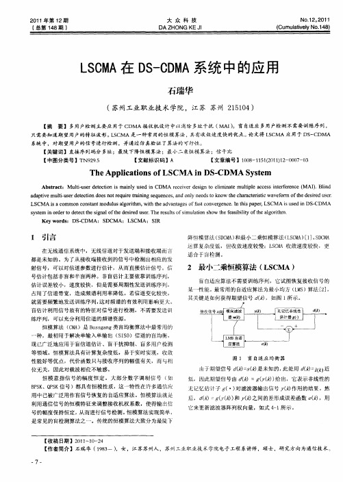
个用户的扩频序列 ,扩频系数 为 Ⅳ ,即 s c = [l 2 C,c …, CkT N]。发送端 发送 的信号 a为所有 个用 户信号扩频后的叠 c 加,如式 4 9所示 。 -
在 [] 5 中详细地分析 了 LC A算法性能 , SM 这里只给出了算 法分析 的主要结果 , 说明 L C A的全局稳定性和全局收敛性。 SM
给定任意 ( , 通过更新公式产生下一次迭代 的均衡权
向量 r k 1 ,则以下不等 式成立 : (+)
口∑ r = ^ c d固
(6 4) —
(7 4 ) —
积的定义 ,则发送信号 a可表示为如下形式:
(9 4) —
o 1, ; I( I-I(+); N <1( J I k I-yk 1I y ), I I≤
【 收稿 日期 】2 1 - 0 2 0 1 1-4
【 者简 介】石瑞 华 ( 9 3 ) 作 18 一 ,女 ,江 苏苏州人 ,苏州工业职 业技 术学院电子 工程 系讲师 ,硕士 ,研究方向为通信技术。
一
7一
e: ) ( g y( l () k ) ( 一)
w k 1=wk + ()’i ( + ) () 七P()J . }
CM D A系统通过码序列来区分不 同的用户 , 它为每个用户 分配各 自特 定的码 序列 ,码序列之间相互 ( )正交。接收 准 端必须具有与发送端完全一致的码序列,用于对接 收信号进 行相关检 测以恢复出发射信号 。 CM D A可 以分为直接序列扩频 ( S 、调频扩频 ( H D) F )和 跳时扩频 ( H T )三种方 式。D — D ̄ ( S CI 直接序列码分 多址 )是  ̄ 最基 本的 C M D A实现方式, 的工作原理是把需要传送 的信息 它
【CN109978028A】一种基于集成深度学习的特定辐射源识别方法【专利】
(19)中华人民共和国国家知识产权局(12)发明专利申请(10)申请公布号 (43)申请公布日 (21)申请号 201910186536.X(22)申请日 2019.03.12(71)申请人 北京理工大学地址 100081 北京市海淀区中关村南大街5号(72)发明人 张焱 何遵文 俞江 张万成 季子杰 (74)专利代理机构 北京理工正阳知识产权代理事务所(普通合伙) 11639代理人 唐华(51)Int.Cl.G06K 9/62(2006.01)G06N 3/04(2006.01)G06N 3/08(2006.01)G01R 29/08(2006.01)(54)发明名称一种基于集成深度学习的特定辐射源识别方法(57)摘要一种基于集成深度学习的特定辐射源识别方法,属于信号处理以及辐射源识别技术领域。
所述识别方法包括如下步骤:1)测量特定辐射源发射信号生成原始数据集;2)从原始数据集信号生成三维图像;3)将三维图像转换为二维图像;4)将二维图像送入学习器生成对应的识别模型;5)将待识别信号集生成三维图像;6)将三维图像生成二维图像;7)将二维图像送入4)生成的识别模型中得到辐射源识别结果和对应后验概率;8)将识别结果的后验概率使用集成学习方法进行再学习和训练,得到待识别信号的最终识别结果。
所述方法用于电子情报侦察、无线频谱管理和无线网络安全管理,具有运算简单和识别精度较高的优点。
权利要求书2页 说明书7页 附图4页CN 109978028 A 2019.07.05C N 109978028A权 利 要 求 书1/2页CN 109978028 A1.一种基于集成深度学习的特定辐射源识别方法,其特征在于:包括如下步骤:步骤1)用信号采集装置测量M个特定辐射源的发射信号生成原始数据集,并保存生成的原始数据集;其中,信号采集装置对每个特定辐射源采集K个信号,因此,原始数据集中包含M个特定辐射源的发射信号,共有K*M个信号;其中,步骤1)保存的原始数据集为已知归属种类的原始数据集,且原始数据集中的信号为一段时间序列,且时间序列中的每一个数据为复信号;步骤2)初始化k=1;步骤3)对原始数据集中第k个信号中取长度为N的一段信号X N k,分别进行3A、3B以及3C 操作,生成3个三维图像,具体为:3A、对X N k进行小波分析,得到小波系数,生成第k个三维小波系数图像;3B、对X N k进行双谱分析,得到双谱系数,生成第k个三维双谱系数图像;3C、对X N k进行三谱分析,得到三谱系数,生成第k个三维三谱系数图像;至此,3A、3B以及3C生成的1个三维小波系数图像、1个三维双谱系数图像、1个三维三谱系数图像合称为3个三维图像;步骤4)判断循环计数值k是否已经达到计数最大值K*M,并决定是否完成本方法,具体为:4.1若否,则k=k+1,跳至步骤3);4.2若是,则得到3K*M个三维图像,跳至步骤5);步骤5)从步骤4)所得的3K*M个三维图像中各选取L个合适视角进行投影,得到3K*M*L 个二维图像;其中,合适视角选取原则:三维小波系数图像投影得到二维小波图像,选取视角范围为(-88°,0°)至(-92°,0°),以及(88°,0°)至(92°,0°);三维双谱系数图像投影得到二维双谱图像,选取视角范围为(-88°,0°)至(-92°,0°),以及(-43°,0°)至(-48°,0°),以及(43°,0°)至(48°,0°);三维三谱系数图像投影得到二维三谱图像,选取视角范围为(-88°,0°)至(-92°,0°),以及(-43°,0°)至(-48°,0°),以及(43°,0°)至(48°,0°);由三维图像生成二维图像时,每一类选取L个视角生成多组二维图像;步骤6)将由原始数据集经步骤5)生成的二维图像送入学习器进行学习,生成对应的识别模型;步骤7)将K设置为[K*1/S],并将j初始化为1;步骤8)用信号采集装置重新测量M个特定辐射源的发射信号生成待识别信号集,并保存生成的待识别信号集;其中,信号采集装置对每个特定辐射源采集K个信号,因此,待识别信号集中包含M个特定辐射源的发射信号,共有K*M个信号且保存的待识别信号不知归属种类;步骤9)对待识别信号集中第j个信号中取长度为N的一段信号Y N j,分别进行9A、9B以及9C操作,生成3个三维图像,具体为:9A、对Y N j进行小波分析,得到小波系数,生成第j个三维小波系数图像;9B、对Y N j进行双谱分析,得到双谱系数,生成第j个三维双谱系数图像;2。
《2024年面向深度学习系统的模糊测试技术研究进展》范文

《面向深度学习系统的模糊测试技术研究进展》篇一一、引言深度学习是现代人工智能的重要基石,被广泛应用于计算机视觉、语音识别、自然语言处理等领域。
然而,随着深度学习系统的日益普及,其安全问题也逐渐浮现。
由于深度学习系统的复杂性和独特性,传统的软件测试方法往往难以对其进行全面有效的测试。
因此,面向深度学习系统的模糊测试技术成为了研究的热点。
本文将就面向深度学习系统的模糊测试技术的相关研究进展进行综述。
二、模糊测试技术概述模糊测试(Fuzz Testing)是一种通过输入随机或伪随机数据来检测程序错误和安全漏洞的测试方法。
在深度学习系统中,模糊测试技术主要通过对模型进行输入数据的扰动,观察模型的输出和行为,从而发现模型可能存在的漏洞和错误。
三、面向深度学习系统的模糊测试技术研究进展1. 输入数据的生成与优化在模糊测试中,输入数据的生成与优化是关键。
针对深度学习系统,研究者们提出了多种生成输入数据的方法,如基于遗传算法的输入生成、基于粒子群优化的输入优化等。
这些方法能够生成更加复杂、多样化的输入数据,从而更好地检测出深度学习系统的潜在问题。
2. 模糊测试技术的改进传统的模糊测试技术主要针对的是二进制程序,对于深度学习系统而言,其模型结构和数据特性都与传统程序有所不同。
因此,研究者们对模糊测试技术进行了改进,如基于梯度的模糊测试、基于模型覆盖率的模糊测试等。
这些改进的模糊测试技术能够更好地适应深度学习系统的特性,提高测试的效率和准确性。
3. 针对特定模型的模糊测试针对不同类型的深度学习模型,如卷积神经网络、循环神经网络、生成对抗网络等,研究者们也开展了相应的模糊测试研究。
这些研究主要针对模型的特定结构和行为进行测试,以期发现更加深入的潜在问题。
四、研究挑战与未来方向虽然面向深度学习系统的模糊测试技术取得了一定的研究成果,但仍面临诸多挑战。
首先,如何生成更加复杂、多样化的输入数据仍是研究的难点。
其次,如何将传统的模糊测试技术与深度学习系统的特性相结合,提高测试的效率和准确性也是一个重要的问题。
空管二次雷达S模式询问机目标捕获与监视实现方案
达系统 ,该系统最显著的特点是采用了问 - 答式的 协同识别方式 。
传统的二次监视雷达系统采用 A/ C 工作模式 , 分别用于监视飞机的编号和高度 ,初期的系统存在 大量的窜扰 、混扰 、旁瓣干扰 。20 世纪 60 年代以 后 ,随着单脉冲体制 、询问旁瓣抑制 、接收旁瓣抑制 等技术的引入 ,二次雷达系统内部存在的窜扰 、混 扰 、旁瓣干扰等固有干扰造成的不利影响在一定程 度上得到缓解 ,使得该系统在世界各地的空中交通
Abstract :An engineering implementation method is proposed for air traffic control (ATC) system to capture and tail mode S airborne targets using secondary surveillance radar(SSR) . Either practical conditions of the mode S interrogator′s employment or concerned standards of ICAO ( International Civil Aviation Organization) Annex10 are taken into consideration in this project . A combined and compatible technique is employed to surveille air2 borne targets completely in transitional period. Self - adapted method of random capture is employed to capture and lock mode S aircraft . Multi - mode S targets in the same antenna beam are interrogated and tailed using time arrangement technique. The method has been applied and verified in a new developed mode S SSR inter2 rogator ,and the system runs well . Key words :air traffic control (ATC) ; secondary surveillance radar (SSR) ;interrogator ; mode S ;target capture
NuttX OS意识型监控手册说明书

OS Awareness Manual NuttX Release 09.2023TRACE32 Online HelpTRACE32 DirectoryTRACE32 IndexTRACE32 Documents ......................................................................................................................OS Awareness Manuals ................................................................................................................OS Awareness Manual NuttX (1)Overview (3)Brief Overview of Documents for New Users3 Supported Versions4Configuration (5)Quick Configuration Guide6 Hooks & Internals in NuttX6Features (7)Display of Kernel Resources7 Task Stack Coverage7 Task-Related Breakpoints8 Task Context Display9 Dynamic Task Performance Measurement9 Task Runtime Statistics10 Function Runtime Statistics11 NuttX specific Menu12NuttX Commands (13)TASK.Task Display tasks13 TASK.BuiLTinAPP Display built-in applications13NuttX PRACTICE Functions (14)TASK.CONFIG()OS Awareness configuration information14Version 09-Oct-2023 OverviewThe OS Awareness for NuttX contains special extensions to the TRACE32 Debugger. This manualdescribes the additional features, such as additional commands and statistic evaluations.Brief Overview of Documents for New UsersArchitecture-independent information:•“Training Basic Debugging” (training_debugger.pdf): Get familiar with the basic features of a TRACE32 debugger.•“T32Start” (app_t32start.pdf): T32Start assists you in starting TRACE32 PowerView instances for different configurations of the debugger. T32Start is only available for Windows.•“General Commands” (general_ref_<x>.pdf): Alphabetic list of debug commands.Architecture-specific information:•“Processor Architecture Manuals”: These manuals describe commands that are specific for the processor architecture supported by your Debug Cable. T o access the manual for your processorarchitecture, proceed as follows:-Choose Help menu > Processor Architecture Manual.•“OS Awareness Manuals” (rtos_<os>.pdf): TRACE32 PowerView can be extended for operating system-aware debugging. The appropriate OS Awareness manual informs you how to enable theOS-aware debugging.Supported VersionsCurrently NuttX is supported for the following versions:•All NuttX versions on ARM/Cortex.ConfigurationThe TASK.CONFIG command loads an extension definition file called “nuttx.t32” (directory“~~/demo/<processor>/kernel/nuttx”). It contains all necessary extensions.Automatic configuration tries to locate the NuttX internals automatically. For this purpose all symbol tables must be loaded and accessible at any time the OS Awareness is used.If you want to have dual port access for the display functions (display “On The Fly”), you have to mapemulation or shadow memory to the address space of all used system tables.For system resource display and trace functionality, you can do an automatic configuration of the OSAwareness. For this purpose it is necessary that all system internal symbols are loaded and accessible at any time, the OS Awareness is used. Each of the TASK.CONFIG arguments can be substituted by '0', which means that this argument will be searched and configured automatically. For a fully automatic configuration omit all arguments:TASK.CONFIG nuttx.t32Quick Configuration GuideTo get a quick access to the features of the OS Awareness for NuttX with your application, follow this roadmap:1.Copy the files “nuttx.t32” and “nuttx.men” to your project directory.(from TRACE32 directory “~~/demo/<processor>/kernel/nuttx”).2.Start the TRACE32 Debugger.3.Load your application as usual.4.Execute the command:TASK.CONFIG nuttx.t32See “Configuration”.5.Execute the command:MENU.ReProgram nuttx.menSee “NuttX Specific Menu”.6.Start your application.Now you can access the NuttX extensions through the menu.In case of any problems, please carefully read the previous Configuration chapter.Hooks & Internals in NuttXNo hooks are used in the kernel.For detecting the current running task, the kernel symbol “g_readytorun” is used.For retrieving the kernel data structures, the OS Awareness uses the global kernel symbols and structure definitions. Ensure that access to those structures is possible every time when features of the OSAwareness are used.FeaturesThe OS Awareness for NuttX supports the following features.Display of Kernel ResourcesThe extension defines new commands to display various kernel resources. Information on the following NuttX components can be displayed:TASK.Task Display tasksTASK.BuiLTinApp Display the built-in application within NuttX imageFor a detailed description of each command, refer to chapter “NuttX Commands”.When working with emulation memory or shadow memory, these resources can be displayed “On The Fly”,i.e. while the target application is running, without any intrusion to the application. If using this dual portmemory feature, be sure that emulation memory is mapped to all places where NuttX holds its tables.When working only with target memory, the information will only be displayed if the target application is stopped.Task Stack CoverageFor stack usage coverage of tasks, you can use the TASK.STacK command. Without any parameter, this command will open a window displaying with all active tasks. If you specify only a task magic number as parameter, the stack area of this task will be automatically calculated.T o use the calculation of the maximum stack usage, a stack pattern must be defined with the command TASK.STacK.PATtern (default value is zero).T o add/remove one task to/from the task stack coverage, you can either call the TASK.STacK.ADD or TASK.STacK.ReMove commands with the task magic number as the parameter, or omit the parameter and select the task from the TASK.STacK.* window.It is recommended to display only the tasks you are interested in because the evaluation of the used stack space is very time consuming and slows down the debugger display.Task-Related BreakpointsAny breakpoint set in the debugger can be restricted to fire only if a specific task hits that breakpoint. This is especially useful when debugging code which is shared between several tasks. T o set a task-relatedbreakpoint, use the command:Break.Set<address>|<range>[/<option>] /TASK <task>Set task-related breakpoint.•Use a magic number, task ID, or task name for <task>. For information about the parameters, see “What to know about the Task Parameters” (general_ref_t.pdf).•For a general description of the Break.Set command, please see its documentation.By default, the task-related breakpoint will be implemented by a conditional breakpoint inside the debugger.This means that the target will always halt at that breakpoint, but the debugger immediately resumesexecution if the current running task is not equal to the specified task.NOTE:T ask-related breakpoints impact the real-time behavior of the application.On some architectures, however, it is possible to set a task-related breakpoint with on-chip debug logic that is less intrusive. T o do this, include the option /Onchip in the Break.Set command. The debugger then uses the on-chip resources to reduce the number of breaks to the minimum by pre-filtering the tasks.For example, on ARM architectures: If the RTOS serves the Context ID register at task switches, and if the debug logic provides the Context ID comparison, you may use Context ID register for less intrusive task-related breakpoints:eContextID ON Enables the comparison to the whole Context ID register.Break.CONFIG.MatchASID ON Enables the comparison to the ASID part only.TASK.List.tasks If TASK.List.tasks provides a trace ID (traceid column), thedebugger will use this ID for comparison. Without the trace ID,it uses the magic number (magic column) for comparison.When single stepping, the debugger halts at the next instruction, regardless of which task hits thisbreakpoint. When debugging shared code, stepping over an OS function may cause a task switch and coming back to the same place - but with a different task. If you want to restrict debugging to the current task, you can set up the debugger with SETUP.StepWithinTask ON to use task-related breakpoints for single stepping. In this case, single stepping will always stay within the current task. Other tasks using the same code will not be halted on these breakpoints.If you want to halt program execution as soon as a specific task is scheduled to run by the OS, you can use the Break.SetTask command.Task Context DisplayY ou can switch the whole viewing context to a task that is currently not being executed. This means that all register and stack-related information displayed, e.g. in Register, Data.List, Frame etc. windows, will refer to this task. Be aware that this is only for displaying information. When you continue debugging theapplication (Step or Go), the debugger will switch back to the current context.T o display a specific task context, use the command:Frame.TASK[<task>]Display task context.•Use a magic number, task ID, or task name for <task>. For information about the parameters, see “What to know about the Task Parameters” (general_ref_t.pdf).•To switch back to the current context, omit all parameters.T o display the call stack of a specific task, use the following command:Frame /Task <task>Display call stack of a task.If you’d like to see the application code where the task was preempted, then take these steps:1.Open the Frame /Caller /Task<task> window.2.Double-click the line showing the OS service call.Dynamic Task Performance MeasurementThe debugger can execute a dynamic performance measurement by evaluating the current running task in changing time intervals. Start the measurement with the commands PERF.Mode TASK and PERF.Arm, and view the contents with PERF.ListTASK. The evaluation is done by reading the ‘magic’ location (= current running task) in memory. This memory read may be non-intrusive or intrusive, depending on the PERF.METHOD used.If PERF collects the PC for function profiling of processes in MMU-based operating systems(SYStem.Option.MMUSPACES ON), then you need to set PERF.MMUSPACES, too.For a general description of the PERF command group, refer to “General Commands Reference Guide P” (general_ref_p.pdf).Task Runtime StatisticsNOTE:This feature is only available, if your debug environment is able to trace taskswitches (program flow trace is not sufficient). It requires either an on-chip tracelogic that is able to generate task information (eg. data trace), or a softwareinstrumentation feeding one of TRACE32 software based traces (e.g. FDX orLogger). For details, refer to “OS-aware Tracing” (glossary.pdf).Based on the recordings made by the Trace (if available), the debugger is able to evaluate the time spent ina task and display it statistically and graphically.T o evaluate the contents of the trace buffer, use these commands:Trace.List List.TASK DEFault Display trace buffer and task switchesTrace.STATistic.TASK Display task runtime statistic evaluationTrace.Chart.TASK Display task runtime timechartTrace.PROfileSTATistic.TASK Display task runtime within fixed time intervalsstatisticallyTrace.PROfileChart.TASK Display task runtime within fixed time intervals ascolored graphTrace.FindAll Address TASK.CONFIG(magic) Display all data access records to the “magic”locationTrace.FindAll CYcle owner OR CYcle context Display all context ID records The start of the recording time, when the calculation doesn’t know which task is running, is calculated as “(unknown)”.All kernel activities up to the task switch are added to the calling task.Function Runtime StatisticsNOTE:This feature is only available, if your debug environment is able to trace taskswitches (program flow trace is not sufficient). It requires either an on-chip tracelogic that is able to generate task information (eg. data trace), or a softwareinstrumentation feeding one of TRACE32 software based traces (e.g. FDX orLogger). For details, refer to “OS-aware Tracing” (glossary.pdf).All function-related statistic and time chart evaluations can be used with task-specific information. The function timings will be calculated dependent on the task that called this function. T o do this, in addition to the function entries and exits, the task switches must be recorded.T o do a selective recording on task-related function runtimes based on the data accesses, use the following command:; Enable flow trace and accesses to the magic locationBreak.Set TASK.CONFIG(magic) /TraceDataT o do a selective recording on task-related function runtimes, based on the Arm Context ID, use the following command:; Enable flow trace with Arm Context ID (e.g. 32bit)ETM.ContextID 32T o evaluate the contents of the trace buffer, use these commands:Trace.ListNesting Display function nestingTrace.STATistic.Func Display function runtime statisticTrace.STATistic.TREE Display functions as call treeTrace.STATistic.sYmbol /SplitTASK Display flat runtime analysisTrace.Chart.Func Display function timechartTrace.Chart.sYmbol /SplitTASK Display flat runtime timechartThe start of the recording time, when the calculation doesn’t know which task is running, is calculated as “(unknown)”.All kernel activities up to the task switch are added to the calling task.NuttX specific MenuThe menu file “nuttx.men” contains a menu with NuttX specific menu items. Load this menu with theMENU.ReProgram command.Y ou will find a new menu called NuttX.•The Display menu items launch the kernel resource display windows.•The Stack Coverage submenu starts and resets the NuttX specific stack coverage and provides an easy way to add or remove tasks from the stack coverage window.In addition, the menu file (*.men) modifies these menus on the TRACE32 main menu bar:•The Trace menu is extended. In the List submenu, you can choose if you want a trace list window to show only task switches (if any) or task switches together with default display.•The Perf menu contains additional submenus for task runtime statistics, task-related function runtime statistics or statistics on task states.NuttX CommandsTASK.TaskDisplay tasksDisplays detailed information about the tasks.“magic” is a unique ID, used by the OS Awareness to identify the task.TASK.BuiLTinAPPDisplay built-in applicationsDisplays the built-in applications within the NuttX image with detailed information.Format:TASK.Task Format:TASK.BuiLTinAPPNuttX PRACTICE FunctionsThere are special definitions for NuttX specific PRACTICE functions.TASK.CONFIG()OS Awareness configuration information Syntax:TASK.CONFIG(magic | magicsize)Parameter and Description:magic Parameter Type: String (without quotation marks).Returns the magic address, which is the location that contains thecurrently running task (i.e. its task magic number).magicsize Parameter Type: String (without quotation marks).Returns the size of the task magic number (1, 2 or 4).Return Value Type: Hex value.。
航天遥感相机TDI CCD成像系统逻辑软件测试平台的设计

VLEL 子 AL_ 电 Y 学 _科
航 天 遥 感 相 机TDI CD成 像 系 统逻 辑 软 件 测 试 平 台 的设 计 C
吕宝林 王 晓东 刘 文光 李丙玉 曲洪丰
长春 10 3 ) 3 0 3 ( 中国科学院 长 春光学精 密机械与物理研究所 吉林
[ 摘
要] 为提 高航天任务 中航天遥感相 机软件 系统工作 的可靠性和 稳定性 ,需要设计专 门的逻辑 软件测试 平台 ,对 软件配 置项 进行独 立、全面 的测试 提 出航
品 代 替 品 ) 和使 F G运 行 的最 小 系 统 即 可 保 证 程 序 正 常运 行 。 出于 模 拟 PA F G 逻辑 软 件工 作 条件 及 测试 全 面 性 的考 虑 ,对C D 控逻 辑F G 和C D PA C主 P A C 数
据 处 理逻 辑 F G软 件 分别 测 试 。在 测试 CD PA C 主控 逻辑 FG 时 ,C D PA C 数据 处 理
辨率 和工 作速度 的 前提 下 比常规 扫描 方式 具有 更高 的灵 敏度 和信 噪 比 。T I D C D 于对 同 一 目标 进 行 多次 曝 光 原理 。因 为 需在 不 同 的位 置 进 行 多 次曝 C基 光 ,T IC D D C 要求 目标 与相机 必 须 实现完 全 的同步 。与一般 线 扫描 传感 器相
F G和 CD 据处 理逻 辑F G 。 PA C数 P A
12 1CD . . C 主控逻 辑 测试 原理
比 ,T IC D D C 借助 了积 分线 来增 加 曝光 时间 。 由于传 感器 内 的信号 存储 与曝 光次 数成 正 比 ,T I 术可 使 在积 分 时 间内收 集 到 的光 子数 增 加 ,所 以T I D技 D
虚拟坐标激光动态跟踪测量系统中光路的琼斯矩阵分析_刘永东
第26卷第5期2000年9月光学技术OPT ICAL T ECHN IQU EVol.26No.5Sept.2000文章编号:1002-1582(2000)05-0413-05虚拟坐标激光动态跟踪测量系统中光路的琼斯矩阵分析*刘永东,王佳,胡朝晖,梁晋文(清华大学精密仪器及机械学系精密测试技术与仪器国家重点实验室,北京100084)摘要:激光跟踪测量系统应用于工业领域,实现动态目标的实时跟踪和虚拟坐标的测量,是测控一体化的计算机集成系统。
推导出该系统中光学系统的琼斯矩阵,采用矢量分析的方法,分析了光学系统(包括分束器、平面跟踪镜和角锥棱镜)对于任意方向入射光偏振态的影响以及光强变化的影响。
在数值仿真的基础上,对光学系统进行优化设计,提高整个系统的跟踪测量性能。
关键词:琼斯矩阵;激光跟踪;矢量中图分类号:T N247文献标识码:AThe Jones matrix analysis of optical beamin virtual coordinate measurement by laser trackingLIU Yong-dong,WAN G Jia,H U Zhao-hui,LIANG Jin-wen(State K ey Labor ator y of Preci sion M easurement T echnolog y and Instruments,Dept.o f P recision I nstr uments,T singhua U niversity,Beijing100084,China) Abstract:Laser tracking and measur ing system is made for dy namic targ et rea-l time measurement in industry field,and it can be made up into computer integr al system w ith both measuring and controlling capacity.T he polar ization effect of the opt-i cal system on a light beam incident in any dir ection is analyzed,and the Jones matrix o f the system is presented.On the base of numerical simulation,the optical system is optimized in order to improve the tracking and measur ing performance o f the whole system.Key words:Jones matrix;laser tracking;v ector1前言运动目标空间位置的实时测量方法种类很多,原理和精度差别较大。
基于功率控制环扰动的DC-DC_变换器能量信息一体化研究

第52卷第7期电力系统保护与控制Vol.52 No.7 2024年4月1日Power System Protection and Control Apr. 1, 2024 DOI: 10.19783/ki.pspc.230885基于功率控制环扰动的DC-DC变换器能量信息一体化研究祝 贺1,2,谢志远1,曹旺斌1,2,胡正伟1(1.华北电力大学电气与电子工程学院,北京 102206;2.河北省电力物联网技术重点实验室(华北电力大学),河北 保定 071003)摘要:针对实现DC-DC变换器之间的信息交互较为复杂的问题,提出了一种基于功率控制环扰动实现其能量信息一体化的方法。
通过在DC-DC变换器的传统功率控制环中叠加二进制频移键控(binary frequency shift keying, 2FSK)信号作为扰动,将数据信息叠加到传统脉冲宽度调制(pulse-width modulation, PWM)信号中,使得该PWM信号同时包含数据信息,实现能量信息一体化。
首先,给出基于2FSK的功率/数据双载波调制以及实时的滑动离散傅里叶变换(sliding discrete Fourier transform, SDFT)解调方案。
然后,通过对Buck变换器的能量信息一体化模型进行小信号建模与分析可知,降低输入阻抗可提升通信的信噪比。
最后搭建一个由两个Buck变换器并联的实验装置进行验证。
实验结果表明在稳态和负载突变的工况下均可实现3 kb/s的稳定通信,验证了所提方法的可行性。
该方法使得DC-DC变换器能同时进行功率变换和数据传输,提升数字化和智能化水平。
关键词:扰动信号;二进制频移键控;滑动傅里叶变换;功率/数据双载波调制;能量信息一体化Power-information integration in DC-DC converters based onpower control loop perturbationZHU He1, 2, XIE Zhiyuan1, CAO Wangbin1, 2, HU Zhengwei1(1. School of Electrical and Electronic Engineering, North China Electric Power University, Beijing 102206, China; 2. Hebei KeyLaboratory of Power Internet of Things Technology (North China Electric Power University), Baoding 071003, China)Abstract: To address the complex issue of information exchange between DC-DC converters, this paper proposes a method that integrates power and information by introducing perturbations into the power control loop. By superimposing binary frequency shift keying (2FSK) signals as perturbations in the traditional power control loop of the DC-DC converters, data information is embedded into the conventional pulse-width modulation (PWM) signal, enabling the PWM signal to simultaneously carry data information, thus achieving the integration of power and information. First, this paper presents a power/data dual carrier modulation scheme based on 2FSK and a real-time sliding discrete Fourier transform (SDFT) demodulation scheme. Subsequently, it is evident from the small-signal modeling and analysis of the power-information integration model of the Buck converter that reducing the input impedance can enhance the signal-to-noise ratio of communication. Finally, an experimental set-up consisting of two parallel Buck converters is constructed for validation.Experimental results demonstrate stable communication at a rate of 3 kb/s in steady-state and load transient conditions, confirming the feasibility of the proposed method. This method enables DC-DC converters to simultaneously perform power conversion and data transmission, thereby enhancing digitization and intelligence levels.This work is supported by the National Natural Science Foundation of China (No. 52177083 and No. 62001166).Key words: perturbation signal; binary frequency shift keying (2FSK); sliding discrete Fourier transform; power/data dual carrier modulation; power-information integration0 引言电力电子变换器作为构建交直流混合电网的核基金项目:国家自然科学基金项目资助(52177083,62001166);河北省省级科技计划项目资助(SZX2020034) 心装备,对信息交互提出了更高的要求[1-3]。
TDA7580中文资料
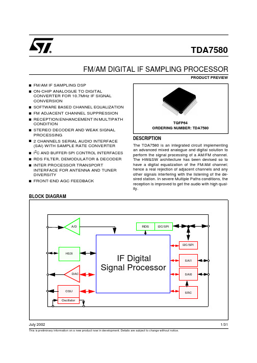
1/31TDA7580July 2002This is preliminary information on a new product now in development. Details are subject to change without notice.s FM/AM IF SAMPLING DSPsON-CHIP ANALOGUE TO DIGITALCONVERTER FOR 10.7MHz IF SIGNAL CONVERSIONs SOFTWARE BASED CHANNEL EQUALIZATION s FM ADJACENT CHANNEL SUPPRESSION s RECEPTION ENHANCEMENT IN MULTIPATH CONDITIONs STEREO DECODER AND WEAK SIGNAL PROCESSINGs2 CHANNELS SERIAL AUDIO INTERFACE (SAI) WITH SAMPLE RATE CONVERTER s I 2C AND BUFFER-SPI CONTROL INTERFACES s RDS FILTER, DEMODULATOR & DECODER sINTER PROCESSOR TRANSPORTINTERFACE FOR ANTENNA AND TUNER DIVERSITYsFRONT-END AGC FEEDBACKDESCRIPTIONThe TDA7580 is an integrated circuit implementing an advanced mixed analogue and digital solution to perform the signal processing of a AM/FM channel.The HW&SW architecture has been devised so to have a digital equalization of the FM/AM channel;hence a real rejection of adjacent channels and any other signals interfering with the listening of the de-sired station. In severe Multiple Paths conditions, the reception is improved to get the audio with high qual-ity.TQFP64ORDERING NUMBER: TDA7580PRODUCT PREVIEWFM/AM DIGITAL IF SAMPLING PROCESSORBLOCK DIAGRAMA/D SAI1SAI0SRCI2C/SPIDACCGU OscillatorI2C/SPIHS3IRDS IF Digital Signal ProcessorTDA7580DESCRIPTION (continued)The algorithm is self-adaptive, thus it requires no “on-the-field” adjustments after the parameters optimization. The chip embeds a Band Pass Sigma Delta Analogue to Digital Converter for 10.7MHz IF conversion from a “tuner device” (it is highly recommended the TDA7515).The internal 24bit-DSP allows some flexibility in the algorithm implementation, thus giving some freedom for customer required features. The total processing power offers a significant headroom for customer’s software requirement, even when the channel equalization and the decoding software is running. The Program and Data Memory space can be loaded from an external non volatile memory via I2C or SPI.The oscillator module works with an external 74.1MHz quartz crystal. It has very low Electro Magnetic Interfer-ence, as it introduces very low distortion, and in any case any harmonics fall outside the Radio bandwidth. The companion tuner device receives the reference clock through a differential ended interface, which works off the Oscillator module by properly dividing down the master clock frequency. That allows the overall system saving an additional crystal for the tuner.After the IF conversion, the digitized baseband signal passes through the Base Band processing section, either FM or AM, depending on the listener selection. The FM Base Band processing comprises of Stereo Decoder, Spike Detection and Noise Blanking. The AM Noise Blanking is fully software implemented.The internal RDS filter, demodulator and decoder features complete functions to have the output data available through either I2C or SPI interface. No DSP support is needed but at start-up, so that RDS can work in back-ground and in parallel with other DSP processing. This mode (RDS-only) allows current consumption saving for low power application modes.An I2C/SPI interface is available for any control and communication with the main micro, as well as RDS data interface. The DSP SPI block embeds a 10 words FIFO for both transmit and receive channels, to lighten the DSP task and frequently respond to the interrupt from the control interface.Serial Audio Interface (SAI) is the ideal solution for the audio data transfer, both transmit and receive: either master or slave. The flexibility of this module gives a wide choice of different protocols, including I2S. Two fully independent bidirectional data channels, with separate clocks allows the use of TDA7580 as general purpose digital audio processor.A fully Asynchronous Sample Rate Converter (ASRC) is available as a peripheral prior to sending audio data out via the SAI, so that internal audio sampling rate (~36kHz and FM/AM mode) can be adapted by upconver-sion to any external rate.An Inter Processor Transport Interface (HS3I, High Speed Synchronous Serial Interface) is also available for a modular system which implements Dual Tuner Diversity, thus enhancing the overall system performance. It is about a Synchronous Serial Interface which exchanges data up to the MPX rate. It has been designed to reduce the Electro Magnetic Interference toward the sensitive analogue signal from the Tuner.General Purpose I/O registers are connected to and controlled by the DSP, by means of memory map.A Debug and Test Interface is available for on-chip software debug as well as for internal registers read/write operation.2/313/31TDA7580ABSOLUTE MAXIMUM RATINGSWarning: Operation at or beyond these limits may result in permanent damage to the device. Normal operation is not guaranteed at theseextremes.Note: 1.V DD3 refers to all of the nominal 3.3V power supplies (V DDH , V OSC , V DDSD ). V DD refers to all of the nominal 1.8V power supplies(V DD , V MTR ).2.During Normal Mode operation VDD3 is always available as specified3.During Fail-safe Mode operation VDD3 may be not available.THERMAL DATASymbol ParameterValue Unit VDD VDD3Power supplies (1)Nom. 1.8V Nom. 3.3V-0.5 to 2.5-0.5 to 4.0V V Analog Input or Output Voltage belonging to 3.3V IO ring (V DDSD , V DDOSC )-0.5 to 4.0V Digital Input or Output Voltage, 5V tolerantNormal (2)Fail-safe (3)-0.5 to 6.50-0.5 to 3.80V V All remaining Digital Input or Output VoltageNom. 1.8V Nom. 3.3V-0.5 to (VDD+0.5)-0.5 to (VDD3+0.5)V T j Operating Junction T emperature Range -40 to 125°C T stgStorage Temperature-55 to 150°CSymbol ParameterValue Unit R th j-ambThermal resistance junction to ambient68°C/WTDA75804/31PIN CONNECTION (Top view)1VHI 2VCM 3VLO 4INP 5INN 6VCMOP 7GNDSD 8GNDOSC9XTI 10XTO 11VDDOSC 12VDDMTR 13CKREFP 14CKREFN 15AGCKEY 16GNDMTR48GND 47VDD46TST3_LRCKR 45TST2_SCKR 44LRCK_LRCKT 43SCLK_SCKT 42SDO041VDDH 40GNDH 39TST1_SDI138TST4_SDI037GPIO_SDO136TESTN 35GND 34VDD 33RESETN64V D D S D63V D D H62G N D H61V D D I S O60G N D59V D D58D B O U T 157D B R Q 156D B I N 155D B C K 154V D D H53G N D H52D B O U T 051D B R Q 050D B I N 049D B C K 032A D D R _S D31I N T30R D S _C S29R D S _I N T28G N D H27V D D H26I Q C H 325I Q C H 224I Q C H 123I Q S Y N C22V D D21G N D20S C L _S C K19M I S O18S D A _M O S I17P R O T S E L _S SI F A D CDEBUG1O S C .T u n e rD S P /R D S I 2C/S P I HS 3IRDSS A IDEBUG0IFADC Modulator Power Supply pins pair Oscillator Power Supply pins pairT uner Clock Out and AGC Keying DAC Power Supply pins pair Core Logic 1.8V Power Supply pins pair I/O Ring 3.3V Power Supply pins pairTDA7580 PIN DESCRIPTIONN°Name Type Description Notes After Reset1VHI A Internally generated IFADC Opamps2.65V (@VDD=3.3V) Reference VoltagePin for external filtering It needs external 22µF and 220nF ceramic capacitors2VCM A Internally generated Common Mode1.65V (@VDD=3.3V) Reference VoltagePin for external filtering It needs external 22µF and 220nF ceramic capacitors3VLO A Internally generated IFADC Opamps0.65V (@VDD=3.3V) Reference VoltagePin for external filtering It needs external 22µF and 220nF ceramic capacitors4INP A Positive IF signal input from T uner 2.0Vpp @VDD=3.3V 5INN A Negative IF signal input from Tuner 2.0Vpp @VDD=3.3V6VCMOP A Internally generated Modulator OpampsCommon Mode 2.65V (@VDD=3.3V)Reference Voltage Pin for externalfiltering It needs external 22µF and 220nF ceramic capacitors7GNDSD G IFADC Modulator Analogue Ground Clean Ground, to bestar-connected tovoltage regulator ground 8GNDOSC G Oscillator Ground Clean Ground, to bestar-connected tovoltage regulator ground9XTI I High impedance oscillator input (quartzconnection) or clock input when inAntenna Diversity slave mode Maximum voltage swing is VDD10XTO O Low impedance oscillator output (quartzconnection)11VDDOSC P Oscillator Power Supply 3.3V12VDDMTR P T uner reference clock and AGCKeyingDAC Power Supply1.8V13CKREFP B T uner reference clock positive output. FM 100kHzAM EU 18kHzWith internal pull_up, onat resetOutput14CKREFN B T uner reference clock negative output. FM 100kHzAM EU 18kHzWith internal pull_up, onat resetOutput15AGCKEY A DAC output for T uner AGCKeying 1.5kohm ±30% outputimpedance. 1Vpp ±1%output dynamic range16GNDMTR G T uner reference clock and AGC keyingDAC Ground5/31TDA75806/3117PROTSEL_SSBDSP0 GPIO for Control Serial Interface (Low: SPI or High: I 2C) selection at device Bootstrap.In SPI protocol mode, after Bootprocedure, SPI Slave Select, otherwise DSP0 GPIO0DSP0 GPIO05V tolerantWith internal pull_up, on at resetInput18SDA_MOSI BControl Serial Interface and RDS IO:- SPI mode: slave data in or master data out for main SPI and RDS SPI data in- I 2C mode: data for main I 2C or RDS I 2C 5V tolerant With internal pull_up, onat reset Input19MISO B SPI slave data out or master data in for main SPI and RDS SPI data outDSP0 GPIO15V tolerantWith internal pull_up, on at resetInput20SCL_SCK BBit clock for Control Serial Interface and RDS 5V tolerant With internal pull_up, onat reset Input21GND G Digital Core Power Ground 22VDD P Digital Core Power Supply1.8V23IQSYNCBHigh Speed Synchronous Serial Interface (HS 3I) clock if HS 3I master mode, else DSP1 GPIO or DSP1 Debug Port Clock (DBOUT1)DSP1 GPIO05V tolerantWith internal pull_up, on at resetInput24IQCH1B High Speed Synchronous SerialInterface (HS 3I) Channel 1 Data if HS 3I master mode, else DSP1 GPIO or DSP1 Debug Port Request (DBRQ1)DSP1 GPIO15V tolerantWith internal pull_up, on at resetInput25IQCH2B High Speed Synchronous SerialInterface (HS 3I) Channel 2 Data if HS 3I master mode, else DSP1 GPIO or DSP1 Debug Port Data In (DBIN1)DSP1 GPIO25V tolerantWith internal pull_down, on at resetInput26IQCH3B High Speed Synchronous SerialInterface (HS 3I) Channel 3 Data if HS 3I master mode, else DSP1 GPIO or DSP1 Debug Port Data Out (DBCK1)DSP1 GPIO35V tolerantWith internal pull_down, on at resetInput27VDDH P3.3V IO Ring Power Supply (HS 3I, I 2C/SPI, RDS, INT)28GNDH G3.3V IO Ring Power Ground (HS 3I, I 2C/SPI, RDS, INT)29RDS_INT B RDS interrupt to external main microprocessor in case of traffic informationDSP1 GPIO45V tolerantWith internal pull_up, on at reset InputN°NameType DescriptionNotesAfter Reset PIN DESCRIPTION (continued)TDA758030RDS_CS B RDS chip select. When RESETN rising,If RDS_CS 0, the RDS’s SPI is selected;else RDS’s I2C DSP1 GPIO55V tolerantWith internal pull_up, onat resetInput31INT I DSP0 External Interrupt5V tolerantWith internalpull_up, on at reset32ADDR_SD B IFS chip master (Low) or slave (High)mode selection, latched in uponRESETN release. It selects the LSB ofthe I2C addresses.Station Detector output DSP0 GPIO25V tolerantWith internalpull_down, on at resetInput33RESETN I Chip Hardware reset, active Low5V tolerantWith internal pull_up 34VDD P Digital Power Supply 1.8V35GND G Digital Power Ground36TESTN I T est Enable pin, active Low With internal pull_up37GPIO_SDO1B DSP0 GPIO for Boot selection or AudioSAI0 output.5V tolerantDSP0 GPIO3With internal pull_up, onat resetInput38TST4_SDI0B Audio SAI0 Data input or test selectionpin in T est Mode 5V tolerantDSP0 GPIO5Withinternal pull_up, on atresetInput39TST1_SDI1B DSP0 GPIO for Boot selection or AudioSAI1 input. T est selection pin in T estMode.5V tolerantDSP0 GPIO4Withinternal pull_up, on atresetInput40GNDH G 3.3V IO Ring Power Ground (Audio SAI,ResetN, T est Pins)41VDDH P 3.3V IO Ring Power Supply (Audio SAI,ResetN, T est Pins)42SDO0B Radio or Audio SAI0 data output5V tolerantWith internal pull_up, onat resetOutput43SCLK_SCKT B SAI0 Receive and Transmit bit clock(master or slave with ASRC); SAI1T ransmit bit clock 5V tolerantWith internal pull_up, onat resetInput44LRCK_LRCKT B SAI0 Receive and Transmit LeftRightclock (master or slave with ASRC); SAI1T ransmit LeftRight clock 5V tolerantWith internal pull_up, onat resetInputN°Name Type Description Notes After ResetPIN DESCRIPTION (continued)7/31TDA75808/3145TST2_SCKRBSAI0 T ransmit bit clock; SAI1 Receive and T ransmit bit clock. Or T est selection pin in T est Mode5V tolerant DSP0 GPIO6With internal pull_up, on at resetInput46TST3_LRCKR B SAI0 T ransmit LeftRight clock; SAI1 Receive and Transmit bit clock. Or T est selection pin in T est Mode DSP0 GPIO75V tolerantWith internal pull_up, on at reset Input47VDD P Digital Core Power Supply 1.8V48GND G Digital Core Power Ground49DBCK0BDebug Port Clock of DSP0 (DBCK0)DSP0 GPIO95V tolerantWith internal pull_down, on at resetInput50DBIN0B Debug Port Data Input of DSP0 (DBIN0)DSP0 GPIO115V tolerantWith internal pull_down, on at resetInput51DBRQ0B Debug Port Request of DSP0 (DBRQ0)DSP0 GPIO 5V tolerantWith internal pull_up, on at resetInput52DBOUT0BDebug Port Data Output of DSP0 (DBOUT0)DSP0 GPIO105V tolerantWith internal pull_up, on at resetInput53GNDH G 3.3V IO Ring Power Ground (Debug Interface, GPIO)54VDDH P 3.3V IO Ring Power Supply (Debug Interface, GPIO)55DBCK1BDSP1 Debug Port Clock (DBCK1) if HS 3I master mode, else High SpeedSynchronous Serial Interface (HS 3I) Channel3 DataDSP1 GPIO95V tolerantWith internal pull_down, on at resetInput56DBIN1B DSP1 GPIO or DSP1 Debug Port Data In (DBIN1) if HS 3I master mode, else High Speed Synchronous Serial Interface (HS 3I) Channel2 Data iDSP1 GPIO115V tolerantWith internal pull_down, on at resetInput57DBRQ1BDSP1 GPIO or DSP1 Debug PortRequest (DBRQ1) if HS 3I master mode, else High Speed Synchronous SerialInterface (HS 3I) Channel1 Data5V tolerant With internal pull_up, onat reset InputN°NameType DescriptionNotesAfter Reset PIN DESCRIPTION (continued)TDA758058DBOUT1B DSP1 GPIO or DSP1 Debug Port DataOut (DBOUT1) if HS3I master mode,else High Speed Synchronous SerialInterface (HS3I) clock DSP1 GPIO105V tolerantWith internal pull_up, onat resetInput59VDD P Digital Core Power Supply 1.8V60GND G Digital Core Power Ground61VDDISO P 3.3V N-isolation biasing supply Clean 3.3V supply to bestar-connected tovoltage regulator62GNDH G 3.3V IO Ring Power Ground (Modulatordigital section)63VDDH P 3.3V IO Ring Power Supply (Modulatordigital section)64VDDSD P 3.3V IFADC Modulator Analogue PowerSupply Clean Power Supply, to be star-connected to 3.3V voltage regulatorN°Name Type Description Notes After ResetPIN DESCRIPTION (continued)I/O TYPEP: Power Supply from Voltage regulator G: Power Ground from Voltage regulator A: Analogue I/OI: Digital InputO: Digital OutputB: Bidirectional I/O I/O DEFINITION AND STATUSZ: high impedance (input)O: logic low outputX: undefined output1: logic high outputOutput PP: Push-Pull/ OD: Open-Drain9/31TDA758010/31RECOMMENDED DC OPERATING CONDITIONSNote: 1.V DDH , V OSC , V DDSD are also indicated in this document as V DD3. All others as V DD .Symbol ParameterCommentMin. Typ.Max.Unit V DD 1.8V Power Supply Voltage Core Power Supply1.7 1.80 1.9V V DDH 3.3V Power Supply Voltage (1)IO Rings Power Supply (with G NDH ) 3.15 3.30 3.45V V OSC 3.3V Power Supply Voltage (1)Oscillator Power Supply (GND OSC ) 3.15 3.30 3.45V V DDSD 3.3V Power Supply Voltage (1)IF ADC Power Supply (with G NDSD ) 3.15 3.30 3.45V V MTR1.8V Power Supply VoltageDAC-Keying and T uner clock Power Supply (with GND MTR )1.71.801.9VGENERAL INTERFACE ELECTRICAL CHARACTERISTICSSymbol ParameterTest ConditionMin.Typ.Max.Unit l ilh Low Level Input Current I/Os@V DD3 (absolute value)V i = 0V (notes 1, 2)without pull-up-down device 1µA l ihh High Level Input Current I/Os@V DD3 (absolute value)V i = V DD3 (notes 1, 2)without pull-up-down device 1µA l il Low Level Input Current I/Os@V DD (absolute value)V i = 0V (notes 1, 3, 4)without pull-up-down device 1µA l ih High Level Input Current I/Os@V DD (absolute value)V i = V DD (notes 1, 3, 4)without pull-up device 1µA I ipdh Pull-down current I/Os @ V DD3V i = V DD3 (note 5)with pull-down device 3.2 6.610.0µA I opuh Pull-up current I/Os @ V DD3V i = 0V(note 6)with pull-up device -10.0-6.6-3.2µA I opul Pull-up current I/Os @ V DDV i = 0V (note 3)with pull-up device-5.4-3.6-1.8µA I aihopAnalogue pin sunk/drawn current on pin1 and pin 6V i = V DD30.95 1.25 1.55mA V i = 0V -6.25-5.0-3.75mA I acmAnalogue pin sunk/drawn current on pin 2V i = V DD3 1.5 2.0 2.5mA V i = 0V -2.5-2.0-1.5mA I ailAnalogue pin sunk/drawn current on pin 3V i = V DD3 3.75 5.0 6.25mA V i = 0V -1.55-1.25-0.95mA I ainAnalogue pin sunk/drawn current on pin 4 and pin 5V i = V DD3243240µA V i = 0V-40-32-24µA I aikAnalogue pin sunk/drawn current on pin 15V i = V DD 0.81.21.6mA V i = 0V (spec absolute value)1µA I ozTri-state Output leakageV o = 0V or V DD3 (note 1)without pull up/down device1µA11/31Note: 1.The leakage currents are generally very small, <1nA. The value given here, 1µA, is the maximum that can occur after an Electro-static Stress on the pin.2.On pins:17 to 20,23 to 26,29 to 33,36 to 39,42 to 46,49 to 52,55 to 58.3.On pins: 13 and 14.4.Same check on the analogue pin 15 (phisically without pull-up-down)5.On pins:25, 26,32,49,50,55,566.On pins:17 to 20,23 to 24,29 to 31,33,36 to 39,42 to 46,51, 52,57, 58LOW VOLTAGE CMOS INTERFACE DC ELECTRICAL CHARACTERISTICSNote: 1.It is the source/sink current under worst case conditions and reflects the name of the I/O cell according to the drive capability.HIGH VOLTAGE CMOS INTERFACE DC ELECTRICAL CHARACTERISTICSNote: 1.It is the source/sink current under worst case conditions and reflects the name of the I/O cell according to the drive capability2.X=4mA for pins 17 to 20,29,30,32,36 to 39,42 to 46; X=8mA for pins 23 to 26,49 to 52,55 to 58.I ozFT5V T olerant T ri-state Output leakage (without pull up/down device)V o = 0V or V dd (note 1)1µA V o = 5.5V 13µA I latchup I/O latch-up current V < 0V , V > V dd200mA V esdElectrostatic ProtectionLeakage, 1µA 2000VSymbol ParameterTest ConditionMin.Typ.Max.Unit V il Low Level Input Voltage 1.70V <=VDD <=1.90V 0.3*V DD3V V ih High Level Input Voltage 1.70V <=VDD <=1.90V 0.8*V DD3V V ol Low level output Voltage I ol = 4mA (notes 1)0.15V V ohHigh level output VoltageI ol = -4mA (notes 1)V DD -0,15VSymbol ParameterTest ConditionMin.Typ.Max.Unit V il Low Level Input Voltage 3.15V <=VDD3<=3.45V 0.8V V ih High Level Input Voltage 3.15V <=VDD3<=3.45V 2.0V V ol Low level output Voltage I ol = XmA (notes 1 and 2)0.15V V ohHigh level output VoltageI ol = -XmA (notes 1 and 2)V DD3-0.15VCURRENT CONSUMPTIONSymbol ParameterTest ConditionMin.Typ.Max.Unit I DD Current through V DD Power SupplyV DD =1.8V ,VDD3=3.3V All digital blocks working 120200mA I DDH Current through V DDH Power SupplyV DD =1.8V ,VDD3=3.3VAll I/Os working with 5pF load 35mA I SD Current through V SD Power SupplyV DD =1.8V ,VDD3=3.3V 364554mA I OSCdcCurrent through V OSC Power SupplyV DD =1.8V ,VDD3=3.3V without quartz5.5810.5mAGENERAL INTERFACE ELECTRICAL CHARACTERISTICS (continued)Symbol ParameterTest ConditionMin.Typ.Max.Unit12/31Note: 74.1MHz internal DSP clock, at T amb = 25°C. Current due to external loads not included.OSCILLATOR CHARACTERISTICSNotes:1.The accuracy of this figure only depends on the quartz frequency precision: high stability oscillatorQUARTZ CHARACTERISTICSDSP COREFM STEREO DECODER CHARACTERISTICSI OSCac Current through V OSC Power SupplyV DD =1.8V ,VDD3=3.3V with quartz in FM mode 111417mA I MTRCurrent through V MTR Power SupplyV DD =1.8V ,VDD3=3.3V5mASymbol ParameterTest Condition Min.Typ.Max.Unit F OSCFM Oscillator Frequency (XTI/XTO)V OSC @ 3.3V 74.1MHz F OSCAMOscillator Frequency (XTI/XTO)V OSC @ 3.3V74.106MHzParameter Name Parameter Value Temperature range-55°C ÷ +125°C Adjustment tolerance (@ 25°C ± 3°C)+/-20ppm Frequency stability (-20°C ÷ +70°C)+/-50ppm Aging @ 25°C5ppm/year Shunt (static) capacitance (Co)<6pFPackages (holders)UM-1; HC-52U; HC-35; HC-48U; HC-49U; HC-50U; HC-51UMode of oscillation A T -3rd Resonance resistance (ESR)<35ohm Oscillation Frequency (without external load)≥74108000 Hz Oscillation Frequency (12pF parallel load)target 74.1MHzSymbol ParameterTest ConditionMin. Typ.Max.Unit F dspMaxMaximum DSP clock frequencyAt 1.7V Core Power Supply and 125°C junction temperature81.5MHzSymbol ParameterTest ConditionMin. Typ.Max.Unit a_ch Channel Separation 50dB THD Total Harmonic Distortion 0.02%(S+N)/NSignal plus Noise to Noise ratio80dBCURRENT CONSUMPTION (continued)Symbol ParameterTest ConditionMin. Typ.Max.UnitSAMPLE RATE CONVERTERMCK = 18.525MHz, F sin/F sout = 0.820445366Symbol Parameter Test Condition Min.Typ.Max.UnitTHD+N T otal Harmonic Distortion +Noise 20Hz to 20kHz, Full Scale, 16 bit inp.-95dB 20Hz to 20kHz, Full Scale, 20 bit inp.-98dB 1 kHz Full Scale, 16 bit inp.-95dB 10 kHz Full Scale, 16 bit inp.-95dB 1 kHz Full Scale, 20 bit inp.-105dB 10 kHz Full Scale, 20 bit inp-98dBDR Dynamic Range 1 kHz -60 dB - 16 bit inp.,A-Weighted98dB1 kHz -60 dB - 20 bit inp.,A-Weighted120dB IPD Interchannel Phase Deviation0Degree f c Cutoff Frequency@ -3 dB HzR p Pass Band Ripple from 0 to 20kHz-0.010.01dBR s Stopband Attenuation@24.1kHz-120dBT g Group Delay Fsout = 44.1 kHz540µsF ratio Sampling Frequency In/Out Ratio Fsout = 44.1 kHz0.7 1.0513/3114/31POWER ON TIMINGFigure 1. Power on and boot sequence using I 2C Figure 2. Power on and boot sequence using SPI VDD3VDD INT RESETN ADDR_SD PROTSEL_SS IFS SLAVE=1RDS_CS GPIO_SDO1IFS MASTER=0I 2C/SP I MASTER=0I 2C/SPI SLAVE=1TST1_SDI1Boot RDS initSW download Tuner dataDataSDA_MOSIt intt sw t resont rsut rhd t tunt datt seq VDD3VDD INT RESETN ADDR_SD PROTSEL_SS IFS SLAVE=1RDS_CS GPIO_SDO1IFS MASTER=0I 2C/SP I MASTER=0I 2C/SPI SLAVE=1TST1_SDI1Boot RDS initSW download Tuner dataDataSDA_MOSIt intt sw t resont rsut rhdt tunt datt seqTiming Description Value Unit t int Maximux delay for INT signal1mst reson Minimum RESETN hold time at 0 after the start-up22mst rsu Minimum data set-up time1µst rhd Minimum data hold time1µst seq Minimum wait time after boot4mst sw Minimum wait time before downloading the Program Software1µst tun Minimum wait time before downloading the software to the FE1µst dat Minimum wait time before using interface protocols1µs15/3116/31SAI INTERFACEFigure 3. SAI TimingsNote T DSP = DSP master clock cycle time = 1/F DSPFigure 4. SAI protocol when RLRS=0; RREL=0; RCKP=1; RDIR=0Timing DescriptionValue Unit T DSP Internal DSP Clock Period (T ypical 1/74.1MHz)13.495ns t sckr Minimum Clock Cycle32*T DSPns t dt SCKR active edge to data out valid 40ns t lrs LRCK setup time 16ns t lrh LRCK hold time 9ns t sdid SDI setup time 16ns t sdih SDI hold time9ns t sckph Minimum SCK high time 0.5*t sckr ns t sckplMinimum SCK low time0.5*t sckrnst sckrt sckplt dtt sdist lrst sckph t lrh t sdihValidLRCKRSDI0-1SCKRValid(RCKP=0)RIGHTLEFTSCKRSDI0-1LRCKR LSB(n-1)MSB(n)MSB-1(n)MSB-2(n)17/31Figure 5. SAI protocol when RLRS=1; RREL=0; RCKP=1; RDIR=1.Figure 6. SAI protocol when RLRS=0; RREL=0; RCKP=0; RDIR=0.Figure 7. SAI protocol when RLRS=0; RREL=1; RCKP=1; RDIR=0.RIGHTLEFTSCKRSDI0-1LRCKR MSB(n-1)LSB(n)LSB+1(n)LSB+2(n)RIGHTLEFTSCKRSDI0-1LRCKRLSB(n-1)MSB(n)MSB-1(n)MSB-2(n)RIGHTLEFTSCKRSDI0-1LRCKRLSB(n-1)MSB(n)MSB-1(n)MSB-2(n)18/31SPI INTERFACEFigure 8. SPI TimingsSymbol DescriptionValue Unit T DSPInternal DSP Clock Period (T ypical 1/74.1MHz)13.495nsMASTERt sclk Minimum Clock Cycle12*T DSPns t dtr Minimum Sclk edge to MOSI valid 40ns t setup Minimum MISO setup time 16ns t hold Minimum MISO hold time 9ns t sclkh Minimum SCK high time 0.5*t sclk ns t sclkl Minimum SCK low time 0.5*t sclk ns t sssetup Minimum SS setup time 40ns t ssholdMinimum SS hold time25nsSLAVEt sclk Minimum Clock Cycle12*T DSPns t dtr Minimum Sclk edge to MOSI valid 40ns t setup Minimum MOSI setup time 16ns t hold Minimum MOSI hold time 9ns t sclkhMinimum SCK high time0.5*t sclknst sclkt sclklt dtrt sssetupt setupt sclkh t hold t ssholdValidMISO SSSCLValid(CPOL=0,CPHA=0)MOSI19/31Figure 9. SPI Clocking Schemet sclkl Minimum SCK high low 0.5*t sclk ns t sssetup Minimum SS setup time 40ns t ssholdMinimum SS hold time20nsSymbol DescriptionValue Unit SCK(#20)SS(#17)(CPOL=0,CPHA=0)(CPOL=0,CPHA=1)(CPOL=1,CPHA=0)(CPOL=1,CPHA=1)SCK(#20)SCK(#20)SCK(#20)MSB 6543210MISO(#19)MOSI(#18)20/31INTER PROCESSOR TRANSPORT INTERFACE FOR ANTENNA DIVERSITY Figure 10. High Speed Synchronous Serial Interface - HS 3INote T DSP = DSP master clock cycle time = 1/F DSPTiming DescriptionValue UnitT DSP Internal DSP Clock Period (T ypical 1/74.1MHz)t mbcc MBC minimum Clock Cycle32*T DSPns t mbco MBC active edge to master data out valid 4ns t mbcs MBC active edge to master synch valid 4ns t sdosSlave Data Out setup time6nsMaster Bit Clock Master Data OutMaster SynchSlave Data Out M2M3S0S1S2S3256 cycles of 74.1MHzt mbcct mbco Master SynchMaster Data OutMaster Bit ClockSlave Data Outt mbcst sdosI2C TIMINGFigure 11. DSP and RDS I2C BUS Timings.Symbol Parameter Test Condition Standard ModeI2C BUSFast ModeI2C BUS Unit Min.Max.Min.Max.F SCL SCLl clock frequency01000400kHz t BUF Bus free between a STOP andStart Condition4.7– 1.3–µst HD:ST A Hold time (repeated) ST ARTcondition. After this period, thefirst clock pulse is generated4.0–0.6–µst LOW LOW period of the SCL clock 4.7– 1.3–µs t HIGH HIGH period of the SCL clock 4.0–0.6–µs t SU:ST A Set-up time for a repeated startcondition4.7–0.6–µs t HD:DA T DA T A hold time0–00.9µst R Rise time of both SDA and SCL signals Cb in pF–100020+0.1C b300nst F Fall time of both SDA and SCL signals Cb in pF–30020+0.1C b300nst SU;STO Set-up time for STOP condition4–0.6–µst SU:DA T Data set-up time250----100nsC b Capacitive load for each bus line–400–400pF21/31。
美国对地观测系统(EOS)中分辨率成像光谱仪(MODIS)遥感数据的特点与应用
万方数据
9,
遥 感 信 息 表 ! 项 目
综 述
术 ( . ,
轨 道 扫 描 频 率 测 绘 带 宽 望 远 镜 体 积 重 量 功 耗 数 据 率 量 化 空 间 分 辨 率 设 计 寿 命
+--- V )
综 述
遥 感 信 息
美 国 对 地 观 测 系 统 ( !"#) 中 分 辨 率 成 像 光 谱 仪 ( $"%&#) 遥 感 数 据 的 特 点 与 应 用
刘 闯 , 葛 成 辉
( 中 国 科 学 院 地 理 科 学 与 资 源 研 究 所 ; 清 华 大 学 电 子 工 程 系 、 宇 航 研 究 中 心 ) 摘 要 : 自 ’((( 年 起 美 国 开 始 了 第 二 阶 段 对 地 观 测 系 统 计 划 , 中 分 辨 率 成 像 光 谱 仪 ( $"%&#) 是 该 计 划 中 最 有 特 色 的 仪 器 之 一 。 通 过 $"%&# 采 集 的 数 据 具 有 )* 个 波 段 和 +,-. / ’---. 地 表 分 辨 率 , 加 上 数 据 以 每 天 上 、 下 午 的 频 率 采 集 和 免 费 接 收 的 数 据 成 为 我 国 地 学 研 究 和 生 态 环 境 监 测 不 可 多 得 的 数 据 资 源 。 本 文 在 对 比 了 $"%&# 与 01233 在 数 据 获 取 政 策 , 使 得 $"%&# 数 据 接 收 、 数 据 格 式 、 数 据 处 理 、 数 据 应 用 等 方 面 的 相 同 与 不 同 点 之 后 , 论 证 了 $"%&# 数 据 在 技 术 方 面 的 主 要 进 展 , 提 出 了 我 国 该 注 意 的 几 个 问 题 。 推 广 使 用 $"%&# 应 关 键 词 : 对 地 观 测 ; 遥 感 数 据 ; 应 用 $"%&# 中 图 分 类 号 :456) 文 献 标 识 码 :7 文 章 编 号 :’-- (+ ---) 8 )’66 ,( 8 --9, 8 -9 是 科 学 家 对 具 有 9, 亿 年 历 史 的 地 球 的 健 康 状 况 第 4!330 就 一 次 进 行 全 面 检 查 和 综 合 诊 断 的 科 学 工 具 ” 。 由 于 4!330 卫 星 每 日 地 方 时 上 午 ’-: 过 境 , 因 此 也 把 它 称 作 地 球 观 )- 时 测 第 一 颗 上 午 星 ( !"# 8 0$’) 。 , <0#0 新 一 代 对 地 观 测 卫 星 的 第 二 颗 星 是 0:;0 卫 星 它 是 美 国 、 巴 西 和 日 本 共 同 合 作 的 产 品 。 该 星 计 划 于 +--年 ’+ 月 发 射 。 星 的 主 要 任 务 也 是 对 地 观 测 , 它 保 留 0:;0 卫 星 上 已 有 的 >!3!# 和 $"%&# 传 感 器 , 并 在 数 据 了 4!330 卫 采 集 时 间 上 与 4!330 形 成 互 补 。 它 也 是 太 阳 同 步 极 轨 卫 星 , 每 日 地 方 时 下 午 过 境 , 因 此 称 作 地 球 观 测 第 一 颗 下 午 星 。 0:;0 卫 星 上 共 载 有 * 个 传 感 器 , 它 们 分 别 ( !"# 8 5$’) 是 : 云 与 地 球 辐 射 能 量 系 统 测 量 仪 8 >!3!# ( >?@ABC DEB FGH , 中 分 辨 率 成 像 光 谱 仪 8 $"%&# !DIFG’ C 3DBJDEF !EHIKL #LCFH.) ( , 大 气 红 外 探 $@BHIDFH 8 IHC@?AFJ@E &.DKJEK #MHNFI@IDBJ@.HFHI ) 测 器 8 0&3#( 0F.@CMGHIJN &ERIDIHB #@AEBHI) , 先 进 微 波 探 测 器 , 巴 西 湿 8 0$#; 8 0( 0BPDENHB $JNI@SDPH #@AEBJEK ;EJF 8 0) 度 探 测 器 8 2#7 ( , 和 地 球 观 测 系 2A.JBJFL #@AEBHI R@I 7IDTJ?) 统 先 进 微 波 扫 描 辐 射 计 8 0$#3 8 !( 0BPDENHB $JNI@SDPH 。 0:;0 增 强 了 对 大 气 的 观 测 力 #NDEEJEK 3DBJ@.HFHI 8 !"#) 度 , 特 别 适 用 于 对 地 球 季 节 性 和 跨 年 度 时 间 尺 度 气 候 变 化 的 研 究 。 此 外 , 美 国 对 地 观 测 系 统 还 将 陆 续 发 射 数 颗 卫 星 , 包 括 以 观 测 大 气 化 学 成 分 为 主 的 0;U0 卫 星 ( 计 划 +--+ 年 ’+ 月 发 射 , 称 作 地 球 观 测 化 学 星 !"# 8 >2!$) , 以 观 测 地 球 冰 雪 、 云 层 和 地 面 高 程 为 主 的 &>!#04 卫 星 ( 计 划 +--’ 年 6 月 发 射 ) , 以 观 测 太 阳 辐 射 和 对 地 球 气 候 影 响 为 主 的 #"3>! 卫 星 ( 计 划 +--+ 年 年 中 发 射 ) 和 以 观 测 陆 地 为 主 的 U0<%#04 8 6 卫 星 ( ’((( 年 发 射 成 功 ) 等 。 在 4!330、 0:;0、 0;U0、 &>!O 六 颗 星 上 共 载 有 +’ 个 包 括 多 光 #04、 #"3>!、 U0<%#04 8 6 等 谱 扫 描 仪 、 微 波 辐 射 计 、 合 成 孔 径 雷 达 等 传 感 器 , 它 们 所 获 得 的 数 据 分 辨 率 分 别 从 ’,. 到 ’---. 不 等 。
脑机接口中一种改进的模式识别方法
脑机接口中一种改进的模式识别方法
杨帮华;颜国正;张永怀;付西光
【期刊名称】《中国生物医学工程学报》
【年(卷),期】2006(025)002
【摘要】为提高脑机接口中脑电识别率,分析了特征提取方面时频特征组合法的缺点,探讨了一种改进的模式识别方法.该方法以样本类平均距离为判据,采用滑动窗优化技术,获取时域均值的最佳时间段和频域功率谱均值的最佳频率段.用经过优化的时域均值和功率谱均值组合作为特征,形成特征向量.基于该特征向量,用神经网络对脑电信号进行分类.以识别正确率为指标,将改进方法与原方法进行对比,实验结果表明改进方法能够提高脑电识别率,具有应用价值.
【总页数】4页(P234-237)
【作者】杨帮华;颜国正;张永怀;付西光
【作者单位】上海交通大学电子信息学院仪器系,上海,200030;上海交通大学电子信息学院仪器系,上海,200030;华瑞科学仪器(上海)有限公司,上海,201821;上海交通大学电子信息学院仪器系,上海,200030
【正文语种】中文
【中图分类】R318;TP183
【相关文献】
1.Web日志挖掘中一种改进的会话识别方法 [J], 黄庆炬;吴珊
2.一种用于脑机接口的模式识别方法 [J], 沈广泽;司峻峰;宁新宝
3.Web日志挖掘中一种事务识别方法的改进 [J], 施建生;伍卫国;陆丽娜
4.同位模式挖掘中一种改进的极大团事务化算法 [J], 杨柽;李勃;谷雨;尚晋霞
5.Web日志挖掘中一种改进的会话识别方法 [J], 周爱武;程博
因版权原因,仅展示原文概要,查看原文内容请购买。
基于卫星增强系统的接收机
基于卫星增强系统的接收机
佚名
【期刊名称】《全球定位系统》
【年(卷),期】2004(029)005
【摘要】美国加州Atmel公司用新的ROM3.0版本,已对其公司生产的16信道GPS芯片进行了升级,以便改进导航精度及完整性,并使其具有更高的灵【总页数】1页(P55)
【正文语种】中文
【中图分类】TN927.2
【相关文献】
1.伪卫星增强系统参考站接收机的测距偏差及优化 [J], 徐博;孙广富;陈华明;欧钢
2.一种基于接收机钟差广义插值法的卫星定位增强算法 [J], 刘成;施浒立;王兆瑞;黄康
3.用于双卫星导航系统用户接收机抗干扰的自适应干扰正交约束下的最佳信号增强算法 [J], 卢艳娥;谈展中;杨军;丁子明;郑玉簋
4.基于北斗卫星导航系统的伪卫星增强技术初探 [J], 张政治;杨胜斌;朱志诚
5.基于卫星增强系统的OEM接收机 [J],
因版权原因,仅展示原文概要,查看原文内容请购买。
用改进的JSHOP2规划器实现机器人多任务优化研究
用改进的JSHOP2规划器实现机器人多任务优化研究陆娜;路飞;张伟【摘要】The key point to consider in the field of home service robots task planning is the optimization ability of multi-tasks and emergency tasks. According to the fact that the JSHOP2 planner is unable to optimize multi-tasks’execution order, an improved JSHOP2 planner is built to realize multi-tasks optimization. Through considering the characteristics of the service tasks in home environment, all the service tasks that can be executed by robot are classified and assigned priority. According to the priority, the improved JSHOP2 planner is built. The simulation results show that the improved JSHOP2 planner is feasible and can improve the intelligence and emergency response ability of home service robots.%家庭服务机器人在进行任务规划时,对环境中的多任务,包括紧急任务的优化能力是机器人任务规划领域需要考虑的重点。
根据JSHOP2规划器不能实现多任务执行顺序优化的缺点,提出了用改进的JSHOP2规划器实现机器人多任务的优化。
采用部分增强型扫描提高跳变时延故障覆盖率的触发器选择方法
采用部分增强型扫描提高跳变时延故障覆盖率的触发器选择方法裴颂伟;李华伟;李晓维【期刊名称】《计算机辅助设计与图形学学报》【年(卷),期】2010(022)009【摘要】选择关键的常规扫描触发器进行置换是采用部分增强型扫描时延测试方法的核心问题.通过定义常规扫描触发器和未检测跳变时延故障的相关度的概念及其计算方法,提出一种触发器选择方法.首先找到被测电路中采用捕获加载方法不可测,但采用增强型扫描可测的跳变时延故障;然后依据常规扫描触发器与这些故障的相关度把少量关键的常规扫描触发器替换成为增强型扫描单元,从而有效地提高电路中跳变时延故障被检测的概率.实验结果表明,采用文中方法在可以接受的硬件开销下能有效地提高被测电路中的跳变时延故障覆盖率.【总页数】7页(P1428-1434)【作者】裴颂伟;李华伟;李晓维【作者单位】中国科学院计算机系统结构重点实验室,北京,100190;中国科学院计算技术研究所,北京,100190;中国科学院研究生院,北京,100049;中国科学院计算机系统结构重点实验室,北京,100190;中国科学院计算技术研究所,北京,100190;中国科学院计算机系统结构重点实验室,北京,100190;中国科学院计算技术研究所,北京,100190【正文语种】中文【中图分类】TP303【相关文献】1.时延故障低成本单跳变测试序列生成器 [J], 杨德才;谢永乐;陈光(礻禹)2.时延转移概率部分未知的网络控制系统鲁棒H∞故障检测 [J], 王燕锋;王培良;蔡志端3.累加器实现的时延故障单跳变测试序列生成 [J], 杨德才;陈光(礻禹);谢永乐4.部分扫描设计中扫描触发器的选择 [J], 忻宏杰;李晓维5.基于累加器的时延故障单跳变测试序列生成 [J], 杨德才;谢永乐;陈光因版权原因,仅展示原文概要,查看原文内容请购买。
- 1、下载文档前请自行甄别文档内容的完整性,平台不提供额外的编辑、内容补充、找答案等附加服务。
- 2、"仅部分预览"的文档,不可在线预览部分如存在完整性等问题,可反馈申请退款(可完整预览的文档不适用该条件!)。
- 3、如文档侵犯您的权益,请联系客服反馈,我们会尽快为您处理(人工客服工作时间:9:00-18:30)。
General guidelines
Commitment All information (answers, queries, and general correspondence) is to be provided in English.
2.3. How many facilities (e.g. universities/hospitals/institutions) for official training for oncology exist in your country? Number ____ Please specify your degree of confidence: Confident Not confident Don’t Know 2.4. What is the total no of *oncologists in your country? Number____ Please specify your degree of confidence: Don’t Know 2.5. Postgraduate specialization and sub-specialization details
DC Survey_Phase II _2007-12-28
ONCOLOGY STATUS IN DEVELOPING COUNTRIES (OS-DC) SURVEY PHASE II 1. GENERAL INFORMATION
Country No. of inhabitants
1.1. What is the minimum number of years required in the medical school before a student graduates as a medical doctor? (Please indicate the minimum no. of years from entry into medical school until the completion of internship i.e. when the candidate will be eligible to get certificate that allows him/her to practice as a doctor). Years ____ Depends on Faculty/University, please indicate average number of years ____ Don’t know 1.2. What is the minimum number of years required for a doctor to receive post graduate qualifications? (Please indicate the minimum no. of years from becoming a doctor to completing training and all requirements to be called a specialist in the basic medical specialties.) Topic General Surgery
Questionnaire compilation Please give a true and fair picture of the national situation. Each answer should have the reference of the source of information used, and the year to which the information refers. For this purpose please fill out the 'SOURCE OF INFORMATION / COMMENTS' section at the end of each section. For any comments or specification of questions please use the 'SOURCE OF INFORMATION / COMMENTS' section at the end of each section. Compilers are kindly requested to strictly follow the instructions. Definition: Medical oncologist A medical oncologist is a physician taking care of cancer patients. He/she has training in internal medicine, with subsequent specialization in the comprehensive management of patients with malignant diseases. His/her training comprises the scientific basis of oncology, prevention, screening, diagnosis, the use and evaluation of specific medical anticancer treatments, and clinical investigation of malignant diseases. He/she is able to use medical therapies and symptomatic, psychological, supportive, palliative, and after care in daily clinical practice to improve the quality-of-life of cancer patients. He/she will be trained and continue to update his/her knowledge in the application of such interventions for optimal benefit, taking into account the psychological and social needs of cancer patients and their families. The standard requirements for training in Medical Oncology are a total training period from five to six (5-6) years, beginning with a training in internal medicine for at least two (2) years, followed by a training program in medical oncology for three (3) to four (4) years. The 3 to 4 year training program in medical oncology must include a minimum of two (2) years full-time clinical training in the diagnosis and management of a broad spectrum of neoplastic diseases. Hansen H, Bajorin D, Muss H, et al: ESMO/ASCO Task Force on Global Curriculum in Medical Oncology, Recommendations for a Global Core Curriculum in Medical Oncology. Ann. Onc., Nov 2004; 15: 1603-1612
Internal Medicine
ห้องสมุดไป่ตู้
Radiology/Radiotherapy
Years ____ Depends on Faculty/University, please indicate average number of years____ Don’t know Years ____ Depends on Faculty/University, please indicate average number of years____ Don’t know Years ____ Depends on Faculty / University, please indicate average number of years____ Don’t know
SOURCE OF INFORMATION/COMMENTS
DC Survey_Phase II _2007-12-28
ONCOLOGY STATUS IN DEVELOPING COUNTRIES (OS-DC) SURVEY PHASE II 2. EDUCATION / TRAINING 2.1. Is oncology officially recognized as a specialty/sub-specialty in your country? Yes No Don’t know If yes, by whom: Government / Ministry of Health National Medical Association Other (pls. specify) _______________ 2.2. What is the minimum number of years required for a postgraduate doctor to become qualified/ recognized as a specialist in medical oncology? (Please indicate the minimum no. of years from becoming a postgraduate doctor to completing training and all requirements to be called a specialist in oncology) With internal medicine training Years____ Depends on Faculty/University, please indicate average number of years____ Don’t know Without internal medicine training Years____ Depends on Faculty/University, please indicate average number of years____ Don’t know