AD7528JN中文资料
ad9858中文资料
特点1 GSPS的内部时钟速度高达2 GHz的输入时钟(可选除以2)集成的10位D/ A转换器<145 dBc / Hz的相位噪声@ 1 kHz偏移输出频率为100兆赫(DAC输出)32位可编程频率寄存器简化8位并行和SPI®串行控制接口自动扫频功能4频剖面3.3 V电源供电功耗2 W典型集成的可编程电荷泵和相快速锁定电路与频率探测器隔离电荷泵提供至5 V综合2 GHz的混频器应用甚高频/超高频劳合成调谐器仪器仪表敏捷时钟合成蜂窝基站跳频合成器雷达SONET / SDH时钟合成一般说明AD9858的是特色经营,以1GSPS的10位DAC的直接数字合成器(DDS)。
AD9858的使用先进的DDS技术,加上内部的高速,高性能D / A转换,形成数字可编程的,完整的高频率合成器能够产生高达400兆赫的频率灵活的模拟输出正弦波。
AD9858的设计提供快速跳频和微调分辨率(32位频率控制字)。
被装入了AD9858的频率调整和控制字通过并行(8位)或串行加载格式。
AD9858的包含一个集成的电荷泵(CP)的合成需要一个高速DDS锁相环(PLL)的功能相结合的应用和相位频率检测器(PFD)。
模拟调音台,还提供片上的应用需要一个DDS,PLL和混频器的组合,如频率转换回路,调谐器,等。
在AD9858的时钟输入还设有一个分2,允许外部时钟,以高达2 GHz的高。
AD9858的指定工作在扩展工业温度范围-40°C至85°C目录功能................................................. .. (1)应用................................................. . (1)一般说明................................................ (1)功能块图............................................... .. (1)AD9858的,电气规格.............................................. .. 3绝对最高评分............................................... . (6)防静电注意事项................................................ . (6)引脚配置................................................ .. (7)引脚功能描述............................................... (8)典型性能特性 (10)论操作............................................... .. (15)概述................................................. (15)构件块................................................ (15)操作模式............................................... .. (17)同步................................................. . (19)在AD9858的编程............................................... (21)AD9858的应用建议 (29)评估委员会................................................ . (30)外形尺寸................................................ .. (31)警告................................................. .. (31)订购指南................................................ .. (31)修订历史11/03-Data表改变从启。
AD7520中文资料
数模(D/A)转换器基础知识在电子技术中,模拟量和数字量的相互转换非常重要。
例如,用电子计算机对生产过程进行控制时,必须先将模拟量转换成数字量,才能送到计算机中去进行运算和处理;然后又要将处理得出的数字量转换为模拟量,才能对被控制的模拟量进行控制。
另外,在数字仪表中,也必须将被测的模拟量转换为数字量才能实现数字显示。
能将模拟量转换为数字量的电路称为模数转换器,简称A/D转换器或ADC;能将数字量转换为模拟量的电路称为数模转换器,简称D/A转换器或DAC。
因此,模数转换器和数模转换器是沟通模拟电路和数字电路的桥梁,也可称之为两者之间的接口。
实际上,在数据传输系统、自动测试设备、医疗信息处理、电视信号的数字化、图像信号的处理和识别、数字通信和语音信息处理等方面都离不开模数转换器和数模转换器。
数模转换器是将一组输入的二进制数转换成相应数量的模拟电压或电流输出的电路。
因为数字量是用二进制代码按数位组合起来表示的,对于有权码,每位代码都有一定的权。
所以,为了将数字量转换成模拟量,必须将每一位的代码按其权的大小转换成相应的模拟量,然后将代表各位的模拟量相加,所得的总模拟量就与数字量成正比,这样便实现了从数字量到模拟量的转换。
这就是组成数模转换器的基本指导思想。
数模转换器根据工作原理基本上可以分为二进制权电阻网络数模转换器和T形电阻网络数模转换器(包括倒T形电阻网络数模转换器)两大类。
权电阻网络数模转换器的优点是电路结构简单,可适用于各种有权码。
缺点是电阻阻值范围太宽,品种较多。
要在很宽的阻值范围内保证每个电阻都有很高的精度是极其困难的。
因此,在集成数模转换器中很少采用权电阻网络。
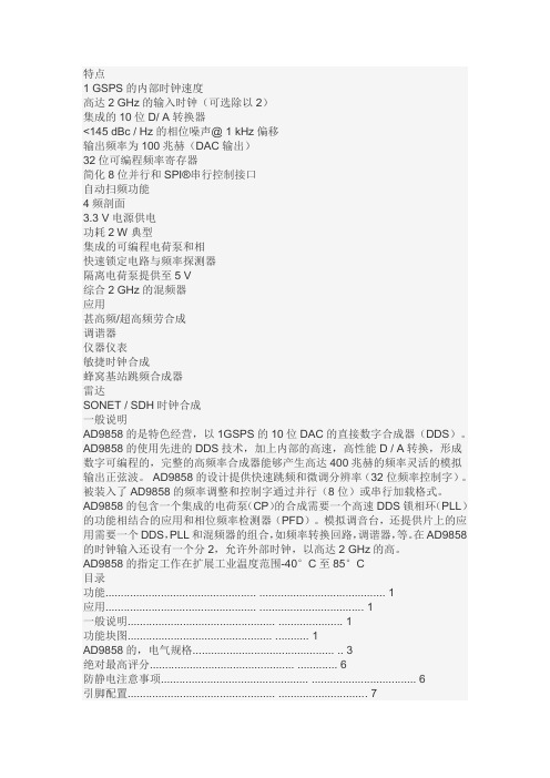
一、倒T形电阻网络数模转换器图11-1所示的是一个四位二进制数倒T形电阻网络数模转换器的原理图。
由图11-1可以看出,这种数模转换器是由倒T形电阻转换网络、模拟电子开关及运算放大器组成。
倒T形电阻网络也是由R和2R两种阻值的电阻构成的。
tC7528
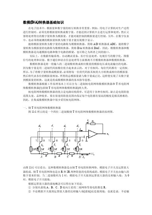
概述:TC7528是双路、8位数字—模拟转换器, TC7528设计成具有单独的片内数据锁存器,其特点包括非常紧密的DAC 至DAC 一致性,两通道DAC 间误差匹配度不超过1%。
数据通过公共输入口传送至两个DAC 数据锁存器的任一个。
控制输入端DACA/DACB 决定哪一个DAC 被加载。
该器件的加载周期与随机存取存储器的写周期类似,能方便地与大多数通用微处理器总线和输出端口相接口。
分段高阶位可以使最高有效位变化期间内的闪变最小,该变化期间内的闪变脉冲最强。
TC7528工作电源为5 V,功耗小于15 mW。
通过TC7528实现的2或4象限乘法功能,是许多微处理器控制的增益设置和信号控制应用的良好选择。
TC7528可工作于电压方式,产生电压输出而不是电流输出。
特性:·易于与微处理器接口; ·片内数据锁存; ·在每个A/D 转换范围内具有单调性; ·可与模拟器件AD7528和 PM7528互换; ·适合于包括与TMS320接口的数字信号处理(DSP)应用的快速控制信号; ·电压方式(VOLTAGEMODE)工作; ·CMOS 工艺制造。
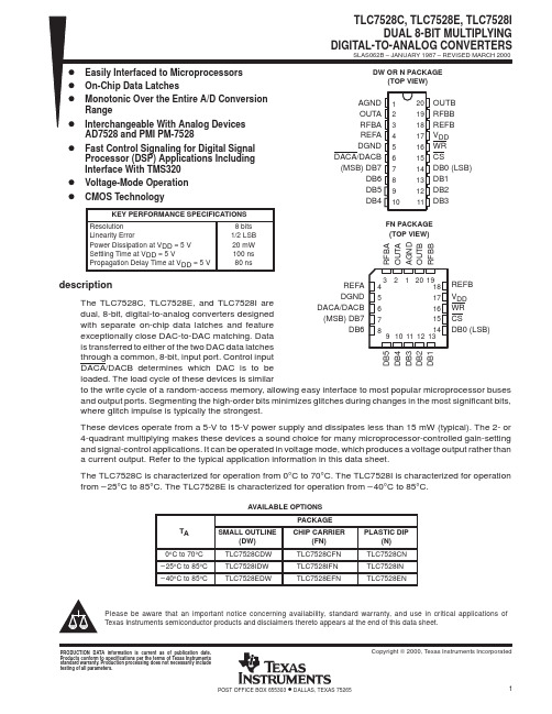
应用:数字控制下的信号细微增加、滤波器、立体声电路、X-Y 方向控制等功能框图:管脚定义:管脚说明:管脚号 符号 说明 1 AGND 模拟电源地 2 OUTA DAC A 路模拟输出端 3 R FB A DAC A 路反馈电阻端 4 V REF A A 路基准电压输入端 5 DGND 数字电源地 6 /DAC A/DAC B DAC 路选择 7~14 DB7(MSB )~ DB0(LSB )八位数据输入高位~低位15 CS 片选线,低电平有效 16 WR 写操作,低电平有效 17 VDD 芯片电源 18 V REF B B 路基准电压输入端 19 R FB B DAC B 路反馈电阻端 20 OUTB DAC B 路模拟输出端规格参数:最大额定范围:(TA = +25°C unless otherwise noted)VDD to AGND . . . . . . . . . . . . . . . . . . . . . . . . . . . . 0 V, +6 V VDD to DGND . . . . . . . . . . . . . . . . . . . . . . . . . . . . 0 V, +6 V AGND to DGND . . . . . . . . . . . . . . . . . . . . . . . . VDD + 0.3 V DGND to AGND . . . . . . . . . . . . . . . . . . . . . . . . VDD + 0.3 V Digital Input Voltage to DGND . . . . . . . –0.3 V, VDD + 0.3 V VPIN2, VPIN20 to AGND . . . . . . . . . . . . . . –0.3 V, VDD + 0.3 V VREF A, VREF B to AGND . . . . . . . . . . . . . . . . . . . . . . . ±5 V VRFB A, VRFB B to AGND . . . . . . . . . . . . . . . . . . . . . . . ±5 V Power Dissipation (Any Package) to +75°C . . . . . . . 450 mW Derates above +75°C by . . . . . . . . . . . . . . . . . . . 6 mW/°C Operating Temperature RangeCommercial (J, K, L) Grades . . . . . . . . . . . –40°C to +85°C Industrial (A, B, C) Grades . . . . . . . . . . . . –40°C to +85°C Extended (S, T, U) Grades . . . . . . . . . . . –55°C to +125°C Storage Temperature . . . . . . . . . . . . . . . .–65°C to +150°C Lead Temperature (Soldering, 10 secs) . . . . . . . . … .+300°C接口逻辑:DAC 部分:两通道的DAC 锁存来自公共的一路8BIT 的数据.控制输入脚DACA/DACB 将会选择哪一路DAC 接受输入脚的8BIT 数据。
AD7537KN中文资料
ppm/°C max Typical value is 1 ppm/°C nA max nA max nA max nA max kΩ min kΩ max % max V min V max µA max µA max pF max V min/V max mA max VIN = VDD DAC A Register loaded with all 0s DAC B Register loaded with all 0s Typical Input Resistance = 14 kΩ Typically ± 0.5%
元器件交易网
a
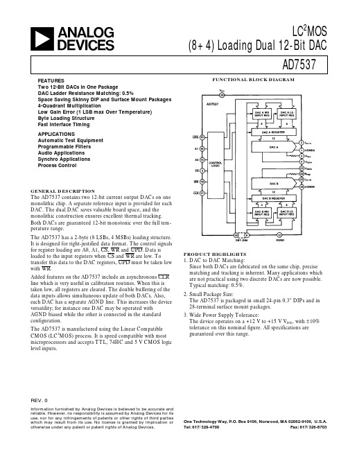
FEATURES Two 12-Bit DACs in One Package DAC Ladder Resistance Matching: 0.5% Space Saving Skinny DIP and Surface Mount Packages 4-Quadrant Multiplication Low Gain Error (1 LSB max Over Temperature) Byte Loading Structure Fast Interface Timing APPLICATIONS Automatic Test Equipment Programmable Filters Audio Applications Synchro Applications Process Control
AC PERFORMANCE CHARACTERISTICS
These characteristics are included for Design Guidance only and are not subject to test. (VDD = +12 V to +15 V; VREFA = VREFB = +10 V; IOUTA = AGNDA = 0 V, IOUTB = AGNDB = 0 V. Output Amplifiers are AD644 except where noted.)
TLC7528
IMPORTANT NOTICETexas Instruments and its subsidiaries (TI) reserve the right to make changes to their products or to discontinue any product or service without notice, and advise customers to obtain the latest version of relevant information to verify, before placing orders, that information being relied on is current and complete. All products are sold subject to the terms and conditions of sale supplied at the time of order acknowledgement, including those pertaining to warranty, patent infringement, and limitation of liability.TI warrants performance of its semiconductor products to the specifications applicable at the time of sale in accordance with TI’s standard warranty. Testing and other quality control techniques are utilized to the extent TI deems necessary to support this warranty. Specific testing of all parameters of each device is not necessarily performed, except those mandated by government requirements.CERTAIN APPLICATIONS USING SEMICONDUCTOR PRODUCTS MAY INVOLVE POTENTIAL RISKS OF DEATH, PERSONAL INJURY, OR SEVERE PROPERTY OR ENVIRONMENTAL DAMAGE (“CRITICAL APPLICATIONS”). TI SEMICONDUCTOR PRODUCTS ARE NOT DESIGNED, AUTHORIZED, OR WARRANTED TO BE SUITABLE FOR USE IN LIFE-SUPPORT DEVICES OR SYSTEMS OR OTHER CRITICAL APPLICATIONS. INCLUSION OF TI PRODUCTS IN SUCH APPLICATIONS IS UNDERSTOOD TO BE FULLY AT THE CUSTOMER’S RISK.In order to minimize risks associated with the customer’s applications, adequate design and operating safeguards must be provided by the customer to minimize inherent or procedural hazards.TI assumes no liability for applications assistance or customer product design. TI does not warrant or represent that any license, either express or implied, is granted under any patent right, copyright, mask work right, or other intellectual property right of TI covering or relating to any combination, machine, or process in which such semiconductor products or services might be or are used. TI’s publication of information regarding any third party’s products or services does not constitute TI’s approval, warranty or endorsement thereof.Copyright © 2000, Texas Instruments Incorporated。
ad7528
NOTES 1 Analog Devices reserves the right to ship side-brazed ceramic in lieu of cerdip. Parts will be marked with cerdip designator “Q.” 2 Processing to MIL-STD-883C, Class B is available. To order, add suffix “/883B” to part number. For further information, see Analog Devices’ 1990 Military Products Databook. 3 N = Plastic DIP; P = Plastic Leaded Chip Carrier; Q = Cerdip; R = SOIC.
REF A
= VREF B = +10 V; OUT A = OUT B = O V unless otherwise noted)
VDD = +15 V TA= +25 °C TMIN, TMAX 8 ±1 ± 1/2 ± 1/2 ±1 ±4 ±2 ±1 ± 0.0035 ± 50 ± 50 8 15 ±1 8 ±1 ± 1/2 ± 1/2 ±1 ±5 ±3 ±1 ± 0.0035 ± 200 ± 200 8 15 ±1 Units Bits LSB max LSB max LSB max LSB max LSB max LSB max LSB max %/ °C max nA max nA max kΩ min kΩ max % max DAC Latches Loaded with 00000000 Input Resistance TC = –300 ppm/°C, Typical Input Resistance is 11 k Ω Test Conditions/Comments
各类电源芯片的简介
电源芯片功能简介电源芯片功能简介........调压器、DC-DC电路和电源监视器引脚及主要特性7800系列三端稳压器(正输岀)输出电压固定的三端系列稳压器;输出电压有5V、6V、7V、8V、9V、10V、12V、15V、18V、20V、24V输出电流1A ; 5〜18V输出的最大电压为35V、20V、24V输出的电大输入电压为40V ; 7800工作温度为-55〜+150 °C, 7800C的为0〜+125 °C;含过流限制和安全工作保护电路。
类似型号:卩A7800、LM7800、MC7800、HA7800、卩PC7800M、NJM7800、TA7800AP、AN7800、CW7800。
78HGA 5A可调稳压器(正输出)输出电压可调的四端正输出稳压器;输出电压围 5 ~24V ;输出电流5A ;功耗50W ;含输出短路电流限制、热过载和安全工作区保护电路。
78L00AC、78L00C 系列三端稳压器(正输出)输出电压固定;输出电压误差有土78L00AC )、± 4% 78L00C );输出电流1〜100mA ; 5V输出的最大输入电压为30V ; 12V、15V输出的最大输入电压为35V ; 24V输出的最输入电压为40V ;含过流限制、过热切断功能。
类似型号:卩A78L00AWC78L00C 、MC78L00AC 、LM78L00AC 、LM78L00C 、卩PC78L00J、TA78L00AP、HA78L00P、AN78L00。
78P12 稳压器输岀电压固定的三端正输岀稳压器;输岀电压12V ;输岀电流10A ;功耗70W ;设输岀短路电流限制、热过载和安全工作区保护装置。
78PGA可调稳压器(正输岀)输出电压可调的四端正输出稳压器;输出电压围 5 ~24 ;输出电流10A ;功耗70W ;设输出短路电流限制、热过载和安全工作区保护装置。
79N00系列三端稳压器(负输岀)输出电压因定的三端系列稳压器;最大输出电流300mA ; 79N04〜79N18的最大输入电压为-35V ;79N04、79N24的最大输入电压为-40V ;功耗8W ;工作温度-29〜+80 C;含过电流限制、过热和安全工作区限制电路。
OB2538中文资料
电压
电流传感输入部分
TLEB
LEB 时间
625
Vth_oc
过流门限
880 910 940
Td_oc
OCP 传送延时
110
Zsense_IN 输入阻抗
50
T_ss
软启动时间
17
频率部分
Freq_Maxnote1 IC 最大频率
55
60
65
Freq_Nom
系统正常开关频
50
率
Freq_startup
INV=0V,Comp=5V
5
OB2538
● 软启动
原边控制高精度恒压/恒流 PWM 控制器
OB2538的特点是在内部设置了软启动功能,主要用于电源启动期间,防止部分 过压造成的异常,即当 VDD 一旦达到 UVLO(OFF)时,控制部分使斜波峰值电流、
电压门限最大,从近似 0 到 0.9V,每一个重启动都对应一个软启动。
● 恒流/恒压工作
7
OB2538
原边控制高精度恒压/恒流 PWM 控制器 VDD 电压由辅助绕组产生,当 VDD 电压低于 UVLO(ON)时?OB?2?53,8 的输出就会 关闭。
8
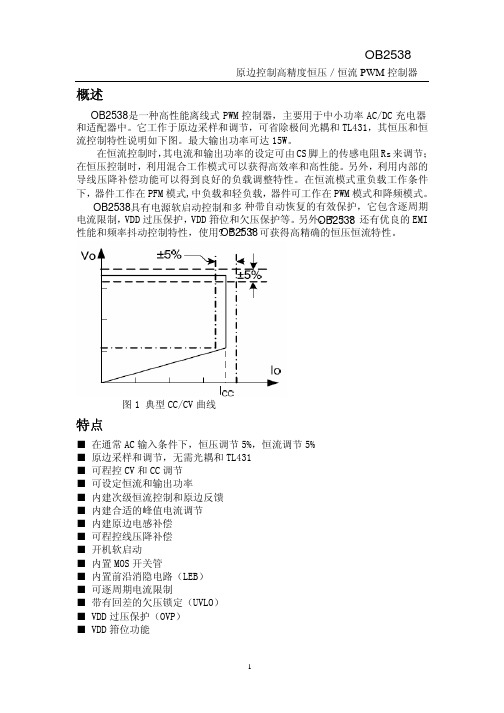
OB2538具有电源软启动控制和多 种带自动恢复的有效保护,它包含逐周期 电流限制,VDD 过压保护,VDD 箝位和欠压保护等。另外O,B?25?3?8 还有优良的 EMI 性能和频率抖动控制特性,使用?OB?2?53?8 可获得高精确的恒压恒流特性。
图 1 典型 CC/CV 曲线
特点
■ 在通常 AC 输入条件下,恒压调节 5%,恒流调节 5% ■ 原边采样和调节,无需光耦和 TL431 ■ 可程控 CV 和 CC 调节 ■ 可设定恒流和输出功率 ■ 内建次级恒流控制和原边反馈 ■ 内建合适的峰值电流调节 ■ 内建原边电感补偿 ■ 可程控线压降补偿 ■ 开机软启动 ■ 内置 MOS 开关管 ■ 内置前沿消隐电路(LEB) ■ 可逐周期电流限制 ■ 带有回差的欠压锁定(UVLO) ■ VDD 过压保护(OVP) ■ VDD 箝位功能
WFP75N08中文资料
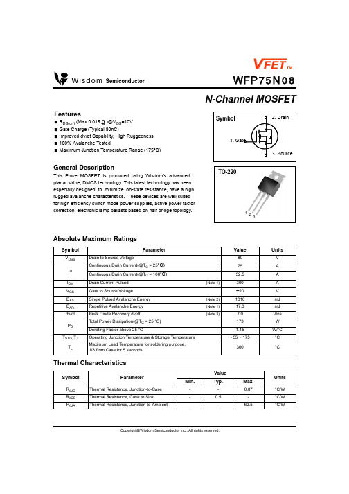
Wisdom Semiconductor
WFP75N08
N-Channel MOSFET
Features
■ RDS(on) (Max 0.015 Ω )@VGS=10V ■ Gate Charge (Typical 80nC) ■ Improved dv/dt Capability, High Ruggedness ■ 100% Avalanche Tested ■ Maximum Junction Temperature Range (175°C)
Gate to Source Voltage
Single Pulsed Avalanche Energy Repetitive Avalanche Energy Peak Diode Recovery dv/dt Total Power Dissipation(@TC = 25 °C) Derating Factor above 25 °C Operating Junction Temperature & Storage Temperature Maximum Lead Temperature for soldering purpose, 1/8 from Case for 5 seconds.
ID, Drain Current [A]
102
101 175℃
25℃ 100
10-1 2
-55℃
※ Notes :
1. VDS = 30V 2. 250µ s Pulse Test
4
6
8
10
VGS, Gate-Source Voltage [V]
Figure 2. Transfer Characteristics
AD7520中文资料
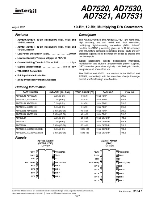
The AD7520/AD7530 and AD7521/AD7531 are monolithic, high accuracy, low cost 10-bit and 12-bit resolution, multiplying digital-to-analog converters (DAC). Intersil’ thin-film on CMOS processing gives up to 10-bit accuracy with TTL/CMOS compatible operation. Digital inputs are fully protected against static discharge by diodes to ground and positive supply.
LINEARITY (INL, DNL) 0.2% (8-Bit) 0.1% (9-Bit) 0.2% (8-Bit) 0.1% (9-Bit)
0.05% (10-Bit) 0.05% (10-Bit)
0.2% (8-Bit) 0.1% (9-Bit) 0.05% (10-Bit) 0.2% (8-Bit) 0.05% (10-Bit)
Thermal Information
Thermal Resistance (Typical, Note 1)
DA转换器AD7520中文资料

AD7520 是十位 CMOS 数模转换器,采用倒 T 形电阻网络。
模开关是CMOS 型的,也同时集成在芯片上,但运算放大器是外接的。
管脚说明AD7520 共有 16 个引脚,各引脚的功能如下。
1 为模拟电流输出端,接到运算放大器的反相输入端。
管脚图2 为模拟电流输出端,一般接“ 地” 。
3 为接“ 地” 端。
4 ~ 13 为十位数字量的输入端。
14 为 CMOS 模拟开关的 +UDD 电源接线端。
15 为参考电压电源接线端,可为正值或负值。
16 为芯片内部一个电阻 R 的引出端,该电阻作为运算放大器的反馈电阻,它的另一端在芯片内部接端。
主要技术指标1 .分辨率分辨率用输入二进制数的有效位数表示。
在分辨率为位的数模转换器中,输出电压能区分个不同的输入二进制代码状态,能给出个不同等级的输出模拟电压。
分辨率也可以用数模转换器的最小输出电压 ( 对应的输入二进制数只有最低位为 1) 与最大输出电压 ( 对应的输入二进制数的所有位全为 1) 的比值来表示。
2 .转换精度数模转换器的转换精度是指输出模拟电压的实际值与理想值之差,即最大静态转换误差。
这误差是由于参考电压偏离标准值、运算放大器的零点漂移、模拟开关的压降以及电阻阻值的偏差等原因所引起的。
3 .输出建立时间从输入数字信号开始,到输出电压或输出电流到达稳定值时所需要的时间,称为输出建立时间。
目前,在不包含参考电压源和运算放大器的单片集成数模转换器中,建立时间一般不超过 1 。
4 .线性度通常用非线性误差的大小表示数模转换器的线性度。
产生非线性误差有两种原因:一是各位模拟开关的压降不一定相等,而且接和接地时的压降也未必相等;二是各个电阻阻值的偏差不可能做到完全相等,而且不同位置上的电阻阻值的偏差对输出模拟电压的影响又不一样。
此外还有电源抑制比、功率消耗、温度系数以及输入高、低逻辑电平的数值等技术指标。
7525中文资料

TOSGAGE Series
X-ray Thickness Gage
General
The X-ray thickness gage is used to measure the thickness of a strip continuously without contacting that strip. This gage uses the fact that the amount of radiation that passes through the strip varies with the thickness of that strip. The TOSGAGE-7525 is a high quality thickness gage for cold rolling achieving outstanding safety, operability, accuracy and cost-performance developed over many years. It has the following features. • Noise immunity is improved by digitizing the signals between the measuring head and the equipment cabinet.
TOSGAGE -7525
• The operation-PC uses Windows® NT, and is a user-friendly PC. • A newly-developed X-ray generator is used, providing extremely accurate measurement results with a quick response time. The TOSGAGE-7525 focuses X-ray beams finely in the strip width direction to improve thickness resolution in the strip width direction, and making it suited to measuring the shape of the section of measured materials. The TOSGAGE-7525 can also be used as a AGC backup for when the fixed thickness gage (TOSGAGE-7521/7522) has failed.
WM8978中文资料
芯片描述 ............................ 14
绪论............................................................... 14 特征............................................................... 14 麦克风输入......................................................... 15 PGA 和 ALC 操作 .....................................................15 线输入(AUXL、AUXR)............................................... 15 ADC................................................................ 15 HI-FI DAC..........................................................15 输出混合器......................................................... 15 音频接口........................................................... 15 控制接口........................................................... 16 时钟配置........................................................... 16 电源控制........................................................... 16 信号输入路线....................................................... 16 麦克风输入......................................................... 16 输入 PGA 音量控制...................................................18 辅助输入........................................................... 19 输入 BOOST .........................................................19 麦克风偏置电路..................................................... 21 模数转换(ADC).................................................... 22 ADC 数字滤波 .......................................................22 可选的高通滤波器................................................... 23 可调陷波滤波器..................................................... 23 数字 ADC 音量控制...................................................24
ADS7828E250;ADS7828EB250;ADS7828E2K5;ADS7828E2K5G4;ADS7828EB2K5;中文规格书,Datasheet资料
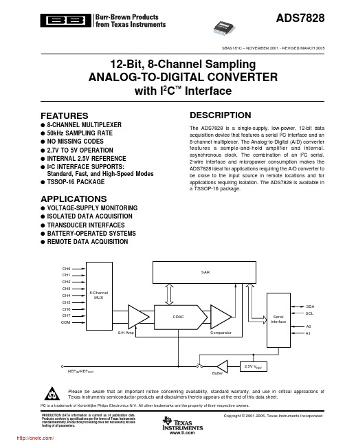
Power Dissipation .................................................... (TJ max – TA)/θJA θJA Thermal Impedance ........................................................ 240°C/W Lead Temperature, Soldering
"
"
"
"
ADS7828EB/2K5 Tape and Reel, 2500
NOTE: (1) For the most current package and ordering information, see the Package Option Addendum at the end of this data sheet, or see the TI web site at .
PIN CONFIGURATION
Top View
CH0 1 CH1 2 CH2 3 CH3 4 CH4 5 CH5 6 CH6 7 CH7 8
ADS7828
TSSOP
16 +VDD 15 SDA 14 SCL 13 A1 12 A0 11 COM 10 REFIN / REFOUT 9 GND
常用AD芯片介绍共7页word资料

目前生产AD/DA的主要厂家有ADI、TI、BB、PHILIP、MOTOROLA等,武汉力源公司拥有多年从事电子产品的经验和雄厚的技术力量支持,已取得排名世界前列的模拟IC生产厂家ADI、TI 公司代理权,经营全系列适用各种领域/场合的AD/DA器件。
1. AD公司AD/DA器件AD公司生产的各种模数转换器(ADC)和数模转换器(DAC)(统称数据转换器)一直保持市场领导地位,包括高速、高精度数据转换器和目前流行的微转换器系统(MicroConvertersTM )。
1)带信号调理、1mW功耗、双通道16位AD转换器:AD7705AD7705是AD公司出品的适用于低频测量仪器的AD转换器。
它能将从传感器接收到的很弱的输入信号直接转换成串行数字信号输出,而无需外部仪表放大器。
采用Σ-Δ的ADC,实现16位无误码的良好性能,片内可编程放大器可设置输入信号增益。
通过片内控制寄存器调整内部数字滤波器的关闭时间和更新速率,可设置数字滤波器的第一个凹口。
在+3V电源和1MHz主时钟时, AD7705功耗仅是1mW。
AD7705是基于微控制器(MCU)、数字信号处理器(DSP)系统的理想电路,能够进一步节省成本、缩小体积、减小系统的复杂性。
应用于微处理器(MCU)、数字信号处理(DSP)系统,手持式仪器,分布式数据采集系统。
2)3V/5V CMOS信号调节AD转换器:AD7714AD7714是一个完整的用于低频测量应用场合的模拟前端,用于直接从传感器接收小信号并输出串行数字量。
它使用Σ-Δ转换技术实现高达24位精度的代码而不会丢失。
输入信号加至位于模拟调制器前端的专用可编程增益放大器。
调制器的输出经片内数字滤波器进行处理。
数字滤波器的第一次陷波通过片内控制寄存器来编程,此寄存器可以调节滤波的截止时间和建立时间。
AD7714有3个差分模拟输入(也可以是5个伪差分模拟输入)和一个差分基准输入。
单电源工作(+3V或+5V)。
AD7908中文资料

6.0 mW Max at 1 MSPS with 3 V Supply 13.5 mW Max at 1 MSPS with 5 V Supply 8 (Single-Ended) Inputs with Sequencer Wide Input Bandwidth: AD7928, 70 dB Min SINAD at 50 kHz Input Frequency Flexible Power/Serial Clock Speed Management No Pipeline Delays High Speed Serial Interface SPI®/QSPI™/ MICROWIRE™/DSP Compatible Shutdown Mode: 0.5 A Max 20-Lead TSSOP Package
4. Flexible Power/Serial Clock Speed Management. The conversion rate is determined by the serial clock, allowing the conversion time to be reduced through the serial clock speed increase. The parts also feature various shutdown modes to maximize power efficiency at lower throughput rates. Current consumption is 0.5 µA max when in full shutdown.
- 1、下载文档前请自行甄别文档内容的完整性,平台不提供额外的编辑、内容补充、找答案等附加服务。
- 2、"仅部分预览"的文档,不可在线预览部分如存在完整性等问题,可反馈申请退款(可完整预览的文档不适用该条件!)。
- 3、如文档侵犯您的权益,请联系客服反馈,我们会尽快为您处理(人工客服工作时间:9:00-18:30)。
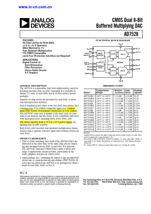
1. DAC-to-DAC matching: since both of the AD7528 DACs are fabricated at the same time on the same chip, precise matching and tracking between DAC A and DAC B is inherent. The AD7528’s matched CMOS DACs make a whole new range of applications circuits possible, particularly in the audio, graphics and process control areas. 2. Small package size: combining the inputs to the on-chip DAC latches into a common data bus and adding a DAC A/DAC B select line has allowed the AD7528 to be packaged in either a small 20-lead DIP, SOIC or PLCC. REV. B
REF A
= VREF B = +10 V; OUT A = OUT B = O V unless otherwise noted)
VDD = +15 V TA= +25 °C TMIN, TMAX 8 ±1 ± 1/2 ± 1/2 ±1 ±4 ±2 ±1 ± 0.0035 ± 50 ± 50 8 15 ±1 8 ±1 ± 1/2 ± 1/2 ±1 ±5 ±3 ±1 ± 0.0035 ± 200 ± 200 8 15 ±1 Units Bits LSB max LSB max LSB max LSB max LSB max LSB max LSB max %/ °C max nA max nA max kΩ min kΩ max % max DAC Latches Loaded with 00000000 I00 ppm/°C, Typical Input Resistance is 11 k Ω Test Conditions/Comments
All Grades Guaranteed Monotonic Over Full Operating Temperature Range Measured Using Internal R FB A and RFB B Both DAC Latches Loaded with 11111111 Gain Error is Adjustable Using Circuits of Figures 4 and 5
AD7528
RFB B OUT B
VREF B
GENERAL DESCRIPTION
ORDERING GUIDE1 Model2 AD7528JN AD7528KN AD7528LN AD7528JP AD7528KP AD7528LP AD7528JR AD7528KR AD7528LR AD7528AQ AD7528BQ AD7528CQ AD7528SQ AD7528TQ AD7528UQ Temperature Ranges –40°C to +85°C –40°C to +85°C –40°C to +85°C –40°C to +85°C –40°C to +85°C –40°C to +85°C –40°C to +85°C –40°C to +85°C –40°C to +85°C –40°C to +85°C –40°C to +85°C –40°C to +85°C –55°C to +125°C –55°C to +125°C –55°C to +125°C Relative Gain Accuracy Error ± 1 LSB ± 1/2 LSB ± 1/2 LSB ± 1 LSB ± 1/2 LSB ± 1/2 LSB ± 1 LSB ± 1/2 LSB ± 1/2 LSB ± 1 LSB ± 1/2 LSB ± 1/2 LSB ± 1 LSB ± 1/2 LSB ± 1/2 LSB ± 4 LSB ± 2 LSB ± 1 LSB ± 4 LSB ± 2 LSB ± 1 LSB ± 4 LSB ± 2 LSB ± 1 LSB ± 4 LSB ± 2 LSB ± 1 LSB ± 4 LSB ± 2 LSB ± 1 LSB Package Options 3 N-20 N-20 N-20 P-20A P-20A P-20A R-20 R-20 R-20 Q-20 Q-20 Q-20 Q-20 Q-20 Q-20
One Technology Way, P.O. Box 9106, Norwood, MA 02062-9106, U.S.A. Tel: 781/329-4700 World Wide Web Site: Fax: 781/326-8703 © Analog Devices, Inc., 1998
元器件交易网
a
FEATURES On-Chip Latches for Both DACs +5 V to +15 V Operation DACs Matched to 1% Four Quadrant Multiplication TTL/CMOS Compatible Latch Free (Protection Schottkys not Required) APPLICATIONS Digital Control of: Gain/Attenuation Filter Parameters Stereo Audio Circuits X-Y Graphics
元器件交易网
AD7528–SPECIFICATIONS (V
Parameter STATIC PERFORMANCE2 Resolution Relative Accuracy Version1 All J, A, S K, B, T L, C, U All J, A, S K, B, T L, C, U TA = +25° C 8 ±1 ± 1/2 ± 1/2 ±1 ±4 ±2 ±1 ± 0.007 ± 50 ± 50 8 15 ±1
VDD DB0 DATA INPUTS DB7
CMOS Dual 8-Bit Buffered Multiplying DAC AD7528
FUNCTIONAL BLOCK DIAGRAM
VREF A RFB A INPUT BUFFER OUT A LATCH DAC A
AGND DAC A/ DAC B CS WR LATCH DGND DAC B CONTROL LOGIC
NOTES 1 Analog Devices reserves the right to ship side-brazed ceramic in lieu of cerdip. Parts will be marked with cerdip designator “Q.” 2 Processing to MIL-STD-883C, Class B is available. To order, add suffix “/883B” to part number. For further information, see Analog Devices’ 1990 Military Products Databook. 3 N = Plastic DIP; P = Plastic Leaded Chip Carrier; Q = Cerdip; R = SOIC.
Gain Temperature Coefficient3 ∆Gain/ ∆Temperature Output Leakage Current OUT A (Pin 2) OUT B (Pin 20) Input Resistance (V REF A, V REF B) VREF A/V REF B Input Resistance Match DIGITAL INPUTS4 Input High Voltage VIH Input Low Voltage VIL Input Current IIN Input Capacitance DB0–DB7 WR , CS, DAC A/DAC B SWITCHING CHARACTERISTICS 3 Chip Select to Write Set Up Time tCS Chip Select to Write Hold Time tCH DAC Select to Write Set Up Time tAS DAC Select to Write Hold Time tAH Data Valid to Write Set Up Time tDS Data Valid to Write Hold Time tDH Write Pulsewidth tWR POWER SUPPLY IDD
V DD = +5 V TMIN, TMAX 8 ±1 ± 1/2 ± 1/2 ±1 ±6 ±4 ±3 ± 0.007 ± 400 ± 400 8 15 ±1
This is an Endpoint Linearity Specification
Differential Nonlinearity Gain Error
The AD7528 is a monolithic dual 8-bit digital/analog converter featuring excellent DAC-to-DAC matching. It is available in skinny 0.3" wide 20-lead DIPs and in 20-lead surface mount packages. Separate on-chip latches are provided for each DAC to allow easy microprocessor interface. Data is transferred into either of the two DAC data latches via a common 8-bit TTL/CMOS compatible input port. Control input DAC A/DAC B determines which DAC is to be loaded. The AD7528’s load cycle is similar to the write cycle of a random access memory and the device is bus compatible with most 8-bit microprocessors, including 6800, 8080, 8085, Z80. The device operates from a +5 V to +15 V power supply, dissipating only 20 mW of power. Both DACs offer excellent four quadrant multiplication characteristics with a separate reference input and feedback resistor for each DAC.