PE6103中文资料
API610第11版标准解读(第三部分)材料篇
API610第11版标准解读(第三部分)材料篇作者根据本⼈在⽯化泵⼀线⼗多年的⼯作及⼯程实践经验,以第11版(等同于ISO13709第2版)为例对API610标准进⾏解读,以帮助中国泵⾏业能更好地理解、设计开发和⽣产API泵,进⽽打造出具有国际级品牌的产品。
注:本⽂中所涉及的条款、表及图号均指API610第11版标准所对应的条款、表及图号。
第⼀部分以安全可靠性,寿命,可操作性,安装及维护⽅⾯解读了,第⼆部分以重点阶段, 下⾯是第三部分:1 离⼼泵常⽤的⾦属材料⼀般将⼯程材料(按化学成分)分为⾦属材料和⾮⾦属材料。
⾦属材料是最重要的⼯程材料,包括⾦属和以⾦属为基的合⾦。
⼯业上将⾦属材料分为⿊⾊⾦属(钢、铸铁)和有⾊⾦属(铝及铝合⾦、铜及铜合⾦等)两⼤部分。
离⼼泵常⽤的⾦属材料有:(1)铸铁。
铸造及切削性能好、耐磨、消振能⼒强,但焊接性能、塑性和韧性差。
离⼼泵上常⽤的铸铁材料有灰铸铁和球墨铸铁,主要⽤做离⼼泵的内壳体(如VS6型泵)、耐磨环、轴承架及底座。
⽽耐磨铸铁可⽤做⾼温油浆泵的衬⾥和叶轮。
(2)碳钢。
碳钢冶炼简便,加⼯容易,价格便宜,⽽且在⼀般情况下能满⾜使⽤性能的要求。
碳钢在普通⼯况、⼀般⽤途的离⼼泵上使⽤⾮常⼴泛,通常⽤做离⼼泵的压⼒泵壳、叶轮、泵轴、(推⼒轴承的)推⼒盘、轴承架及底座等。
(3)合⾦钢。
在碳钢的基础上加⼊⼀些合⾦元素,如硅、锰、铬、镍、钨、钒钛等,根据加⼊的合⾦元素的不同,具有不同的性能。
离⼼泵常⽤的合⾦钢有20MnMo,主要⽤做BB5型泵外筒体(锻件);40Cr、35CrMo及42CrMo,主要⽤做离⼼泵的泵轴和压⼒泵壳紧固件等。
(4)马⽒体不锈钢。
强度和硬度较⾼,具有⼀定的耐蚀性,但塑性和焊接性较差。
离⼼泵上常⽤的马⽒体不锈钢有12Cr13、20Cr13和30Cr13,除了紧固件和密封垫以外,⼏乎可以⽤做离⼼泵所有的零件。
(5)奥⽒体不锈钢。
具有优异的耐蚀性,塑性和韧性好,但强度较低。
6N134中文资料

6N134中⽂资料FeaturesDual Marked with Device Part Number and DSCC Drawing NumberManufactured and Tested on a MIL-PRF-38534 Certified LineQML-38534, Class H and K Five Hermetically Sealed Package Configurations Performance Guaranteed over -55°C to +125°C ? High Speed: 10 M Bit/sCMR: > 10,000 V/µs Typical 1500 Vdc Withstand Test Voltage2500 Vdc Withstand Test Voltage for HCPL-565X High Radiation Immunity 6N137, HCPL-2601, HCPL-2630/-31 Function Compatibility ? Reliability DataTTL Circuit CompatibilityApplicationsMilitary and SpaceHigh Reliability SystemsTransportation, Medical, and Life Critical SystemsLine ReceiverVoltage Level ShiftingIsolated Input Line Receiver Isolated Output Line Driver Logic Ground Isolation Harsh Industrial EnvironmentsIsolation for Computer,Communication, and Test Equipment SystemsDescriptionThese units are single, dual and quad channel, hermetically sealed optocouplers. The products are capable of operation and storage over the full military temperature range and can be purchased as either standard product or with full MIL-PRF-38534 Class Level H or K testing or from the appropri-ate DSCC Drawing. All devices are manufactured and tested on a MIL-PRF-38534 certified line and are included in the DSCC Quali-fied Manufacturers List QML-38534 for Hybrid Microcircuits.Quad channel devices areavailable by special order in the 16 pin DIP through hole packages.Truth Table(Positive Logic)Multichannel DevicesInput Output On (H)L Off (L)HFunctional DiagramMultiple Channel Devices AvailableSingle Channel DIP Input Enable Output On (H)H L Off (L)H H On (H)L H Off (L)LH*See matrix for available extensions.Hermetically Sealed, High Speed,High CMR, Logic Gate Optocouplers Technical Data6N134*81028HCPL-563X HCPL-663X HCPL-565X 5962-98001HCPL-268K HCPL-665X 5962-90855HCPL-560XCAUTION: It is advised that normal static precautions be taken in handling and assembly of this component to prevent damage and/or degradation which may be induced by ESD.V CC V OUTV E GNDThe connection of a 0.1 µF bypass capacitor between V CC and GND is recommended.Selection Guide–Package Styles and Lead Configuration OptionsPackage16 Pin DIP 8 Pin DIP 8 Pin DIP 8 Pin DIP 16 Pin Flat Pack 20 Pad LCCC Lead Style Through Hole Through Hole Through Hole Through Hole Unformed Leads Surface MountChannels 212242Common Channel V CC , GND None V CC , GND V CC , GND V CC , GND None WiringWithstand Test Voltage 1500 Vdc 1500 Vdc 1500 Vdc 2500 Vdc 1500 Vdc 1500 Vdc Agilent Part # & Options Commercial6N134*HCPL-5600HCPL-5630HCPL-5650HCPL-6650HCPL-6630MIL-PRF-38534, Class H 6N134/883BHCPL-5601HCPL-5631HCPL-5651HCPL-6651HCPL-6631MIL-PRF-38534, Class K HCPL-268K HCPL-560K HCPL-563K HCPL-665K HCPL-663K Standard Lead Finish Gold Plate Gold Plate Gold Plate Gold Plate Gold PlateSolder PadsSolder Dipped Option #200Option #200Option #200Option #200Butt Cut/Gold Plate Option #100Option #100Option #100Gull Wing/Soldered Option #300Option #300Option #300Class H SMD Part #Prescript for all below None 5962-None None None None Either Gold or Solder 8102801EX 9085501HPX 8102802PX 8102805PX 8102804FX 81028032XGold Plate 8102801EC 9085501HPC 8102802PC 8102805PC 8102804FCSolder Dipped 8102801EA 9085501HPA 8102802PA 8102805PA81028032A Butt Cut/Gold Plate 8102801UC 9085501HYC 8102802YC Butt Cut/Soldered 8102801UA 9085501HYA 8102802YA Gull Wing/Soldered 8102801TA 9085501HXA8102802ZA Class K SMD Part #Prescript for all below 5962-5962-5962-5962-5962-Either Gold or Solder 9800101KEX 9085501KPX 9800102KPX 9800104KFX 9800103K2XGold Plate 9800101KEC 9085501KPC 9800102KPC 9800104KFCSolder Dipped 9800101KEA 9085501KPA 9800102KPA 9800103K2AButt Cut/Gold Plate 9800101KUC 9085501KYC 9800102KYC Butt Cut/Soldered 9800101KUA 9085501KYA 9800102KYA Gull Wing/Soldered9800101KTA 9085501KXA 9800102KZA*JEDEC registered part.Each channel contains a GaAsP light emitting diode which isoptically coupled to an integrated high speed photon detector. The output of the detector is an open collector Schottky clamped transistor. Internal shields provide a guaranteed common mode transient immunityspecification of 1000 V/µs. For Isolation Voltage applications requiring up to 2500 Vdc, the HCPL-5650 family is also available. Package styles for these parts are 8 and 16 pin DIP through hole (case outlines P andE respectively), and 16 pin surface mount DIP flat pack(case outline F), leadless ceramic chip carrier (case outline 2).Devices may be purchased with a variety of lead bend and plating options. See Selection Guide Table for details. Standard Microcircuit Drawing (SMD)parts are available for each package and lead style.Because the same electrical die (emitters and detectors) are used for each channel of each device listed in this data sheet, absolute maximum ratings, recommended operating conditions, electrical specifications, and performance characteristics shown in the figures are identical for all parts.Occasional exceptions exist due to package variations and limitations,and are as noted. Additionally, the same package assembly processes and materials are used in all devices. These similarities give justification for the use of data obtained from one part torepresent other parts’ performance for reliability and certain limited radiation test results.Outline Drawings16 Pin DIP Through Hole, 2 ChannelsFunctional DiagramsNote: All DIP and flat pack devices have common V CC and ground. Single channel DIP has an enable pin 7. LCCC (leadless ceramic chip carrier) package has isolated channels with separate VCC and ground connections. All diagrams are “top view.”Leaded Device MarkingLeadless Device MarkingNOTE: DIMENSIONS IN MILLIMETERS (INCHES).COMPLIANCE INDICATOR,*DATE CODE, SUFFIX (IF NEEDED)COUNTRY OF MFR.Agilent CAGE CODE*Agilent DESIGNATORDSCC SMD*PIN ONE/ ESD IDENTAgilent P/N DSCC SMD** QUALIFIED PARTS ONLYCOMPLIANCE INDICATOR,*DATE CODE, SUFFIX (IF NEEDED)DSCC SMD*Agilent CAGE CODE*Agilent DESIGNATORCOUNTRY OF MFR.Agilent P/N PIN ONE/ ESD IDENTDSCC SMD** QUALIFIED PARTS ONLYOutline Drawings (continued)16 Pin Flat Pack, 4 Channels8 Pin DIP Through Hole, 2 Channels 2500 Vdc Withstand Test Voltage20 Terminal LCCC Surface Mount,2Channels8 Pin DIP Through Hole, 1 and 2 Channels0.36 (0.014)NOTE: DIMENSIONS IN MILLIMETERS (INCHES).2.29 (0.090) 2.79 (0.110)NOTE: DIMENSIONS IN MILLIMETERS (INCHES).NOTE: DIMENSIONS IN MILLIMETERS (INCHES).NOTE: DIMENSIONS IN MILLIMETERS (INCHES). SOLDER THICKNESS 0.127 (0.005) MAX.Hermetic Optocoupler OptionsRecommended Operating ConditionsParameterSymbol Min.Max.Units Input Current, Low Level, Each Channel I FL 0250µA Input Current, High Level, Each Channel*I FH 1020mA Supply Voltage, OutputV CC 4.55.5VFan Out (TTL Load) Each ChannelN6*Meets or exceeds DSCC SMD and JEDEC requirements.Absolute Maximum Ratings(No derating required up to +125°C)Storage Temperature Range, T S ...................................-65°C to +150°C Operating Temperature, T A..........................................-55°C to +125°C Case Temperature, T C ................................................................+170°C Junction Temperature, T J ...........................................................+175°C Lead Solder Temperature ...............................................260°C for 10 s Peak Forward Input Current, I F PK , (each channel,≤1 ms duration)......................................................................40 mA Average Input Forward Current, I F AVG (each channel)................20 mA Input Power Dissipation (each channel).....................................35 mW Reverse Input Voltage, V R (each channel).........................................5 V Supply Voltage, V CC (1 minute maximum)........................................7 V Output Current, I O (each channel)...............................................25 mA Output Power Dissipation (each channel). (40)mW Output Voltage, V O (each channel)..................................................7 V*Package Power Dissipation, P D (each channel)........................200 mW*Selection for higher output voltages up to 20 V is available.Single Channel Product OnlyEmitter Input Voltage, V E ...............................................................5.5 VNote enable pin 7. An external 0.01 µF to 0.1 µF bypass capacitor must be connected between V CC and ground for each package type.8 Pin Ceramic DIP Single Channel SchematicESD Classification(MIL-STD-883, Method 3015)HCPL-5600/01/0K ...............................................................(?), Class 16N134, 6N134/883B, HCPL-5630/31/3K, HCPL-5650/51, HCPL-6630/31/3K and HCPL-6650/51/5K.......................(Dot), Class 3Electrical Characteristics (T= -55°C to +125°C, unless otherwise specified)*Identified test parameters for JEDEC registered parts.**All typical values are at V CC = 5 V , T A = 25°C. Recommended Operating Conditions (cont’d.)Single Channel Product Only [10]ParameterSymbol Min.Max.Units High Level Enable Voltage V EH 2.0V CC V Low Level Enable VoltageV EL0.8VElectrical Characteristics, (Contd.) T= -55°C to +125°C unless otherwise specifiedSingle Channel Product Only Low Level I EL V CC = 5.5 V,1, 2, 3-1.45-2.0mA Enable Current V E = 0.5 V High Level V EH 1, 2, 3 2.0V10Enable Voltage Low Level V EL 1, 2, 30.8VEnable Voltage*Identified test parameters for JEDEC registered part.**All typical values are at V CC = 5 V , T A = 25°C.Typical Characteristics, T = 25°C, V = 5 VDual and Quad Channel Product Only Input-Input I I-I 0.5nA Relative Humidity = 45%4Leakage CurrentV I-I = 500 V, t = 5 s Resistance (Input-Input)R I-I 1012V I-I = 500 V 4Capacitance (Input-Input)C I-I0.55pF f = 1 MHz4Notes:1. Each channel.2. All devices are considered two-terminal devices; I I-O is measured between all input leads or terminals shorted together and alloutput leads or terminals shorted together.3. Measured between each input pair shorted together and all output connections for that channel shorted together.4. Measured between adjacent input pairs shorted together for each multichannel device.5. t PHL propagation delay is measured from the 50% point on the leading edge of the input pulse to the 1.5 V point on the leadingedge of the output pulse. The t PLH propagation delay is measured from the 50% point on the trailing edge of the input pulse to the1.5 V point on the trailing edge of the output pulse.6. The HCPL-6630, HCPL-6631, and HCPL-663K dual channel parts function as two independent single channel units. Use the singlechannel parameter limits for each channel.7. CM L is the maximum rate of rise of the common mode voltage that can be sustained with the output voltage in the logic low state(V O < 0.8 V). CM H is the maximum rate of fall of the common mode voltage that can be sustained with the output voltage in the logic high state (V O > 2.0 V).8. This is a momentary withstand test, not an operating condition.9. It is essential that a bypass capacitor (0.01 to 0.1 µF, ceramic) be connected from V CC to ground. Total lead length between bothends of this external capacitor and the isolator connections should not exceed 20 mm.10. No external pull up is required for a high logic state on the enable input.11. The t ELH enable propagation delay is measured from the 1.5 V point on the trailing edge of the enable input pulse to the 1.5 Vpoint on the trailing edge of the output pulse.12. The t EHL enable propagation delay is measured from the 1.5 V point on the leading edge of the enable input pulse tothe 1.5 Vpoint on the leading edge of the output pulse.13. Standard parts receive 100% testing at 25°C (Subgroups 1 and 9). SMD and 883B parts receive 100% testing at 25, 125, and-55°C (Subgroups 1 and 9, 2 and 10, 3 and 11, respectively).14. Parameters are tested as part of device initial characterization and after design and process changes. Parameters are guaranteedto limits specified for all lots not specifically tested.15. Not required for 6N134, 6N134/883B, 8102801, HCPL-268K and 5962-9800101 types.16. Required for 6N134, 6N134/883B, 8102801, HCPL-268K and 5962-9800101 types.17. Not required for HCPL-5650, HCPL-5651 and 8102805 types.18. Required for HCPL-5650, HCPL-5651 and 8102805 types only.Figure 1. High Level Output Currentvs. Temperature.5 VV O * C L INCLUDES PROBE AND STRAY WIRING CAPACITANCE. Figure 4. Test Circuit for t PHL and t PLH .*I +5 V OUTPUT V O MONITORING NODEFigure 7. Test Circuit for Common Mode Transient Immunity and Typical Waveforms.11OUTPUT V OMONITORINGNODET A = +125 °C* ALL CHANNELS TESTED SIMULTANEOUSLY.V CCI O = 25 mAFigure 10. Operating Circuit for Burn-In and Steady State Life Tests. Figure 8. Test Circuit for t EHL and t ELH.Figure 9. Enable Propagation Delayvs. Temperature.MIL-PRF-38534 Class H,Class K, and DSCC SMDTest ProgramAgilent’s Hi-Rel Optocouplers arein compliance with MIL-PRF-38534 Classes H and K. Class Hand Class K devices are also incompliance with DSCC drawings81028, 5962-90855 and 5962-98001.Testing consists of 100% screen-ing and quality conformanceinspection to MIL-PRF-38534./doc/4e2d970a03d8ce2f006623a8.htmlData subject to change.Copyright ? 1999 Agilent TechnologiesObsoletes 5968-4743E5968-9407E (10/00)。
斩波稳定高精度低温漂锁存型霍尔效应开关 IC CC6103 4说明书
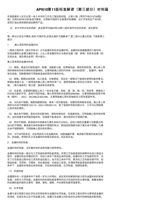
CC6103/4具有斩波稳定功能的高精度, 低温漂锁存型霍尔效应开关概述CC6103/4是一个锁存型的霍尔效应开关IC ,采用先进的BiCMOS 制程制造,具有优异的温度稳定性和很高的抗机械应力性能,产品最高工作温度可以达到150℃。
CC6103/4采用动态失调消除技术以及芯进电子专利保护的温度补偿技术,大幅降低了由于封装应力,环境温度变化等因素造成的失调电压,使产品磁灵敏度持高度的一致性。
CC6103/4包含电源稳压模块,霍尔薄片,信号放大模块,动态失调消除模块以及带有限流保护的功率输出级。
内置的电源稳压模块可以让芯片工作在2.5V 至5.5V 电源电压范围。
当磁场南极靠近芯片CC6103TO / CC6104ST 丝印面,磁场强度达到阈值时,输出低电平。
当磁场北极靠近芯片CC6103TO / CC6104ST 丝印面,磁场强度达到阈值时,输出高电平;当磁场南极靠近芯片CC6103ST / CC6104TO 丝印面,磁场强度达到阈值时,输出高电平。
当磁场北极靠近芯片CC6103ST / CC6104TO 丝印面,磁场强度达到阈值时,输出低电平。
CC6103/4提供TO-92S 和SOT23-3两种封装,均为符合RoHS 规范,产品的使用环境温度范围为-40~150℃。
功能框图动态失调消除放大器预驱动采样保持比较器50KHzLPF基准电压霍尔单元GND特点◆ 开关点高度对称◆ 具有斩波稳定功能,批次之间的一致性好 ◆ 温度稳定性优异,可工作到150℃ ◆ 抗机械应力◆ ESD HBM 4000V 应用◆ 直流无刷马达 ◆ 速度检测 ◆ 线性位置检测 ◆角度检测名称 封装型号 备注 CC6103TO TO-92S 袋装,1000片/包 CC6103ST SOT23-3 卷盘,3000片/卷 CC6104TO TO-92S 袋装,1000片/包 CC6104STSOT23-3卷盘,3000片/卷开关输出 vs. 磁场极性VoutS poleV OHV OLB HB RPB OPN pole CC6103TO / 6104STVoutN poleV V OL 0B HB RP B OPS poleCC6103ST / 6104TO注意: 磁场加在芯片的丝印面管脚描述CC6103XXYYWW132V DD V OUTGND1236103V DDGND V OUTCC6104XXYYWW132V DD V OUTGND1236104V DDGNDV OUT名称 管脚编号 功能 TO-92SSOT23-3V DD 1 1 电源电压 GND 2 3 地 V OUT32输出参数符号数值单位电源电压V DD-0.3~5.5 V输出脚耐压V OUT-0.3~VDD+0.3 V磁场强度 B 无限制Gauss工作环境温度T A-40~150 ℃存储环境温度Ts -50至160 ℃ESD(HBM) 4000 V电气参数参数符号测试环境最小值典型值最大值单位电源电压V DD- 2.5 - 5.5 V静态电流I DD25℃,V DD=5.0V - 2 3 mA输出电流I OUT25℃,V DD=5.0V,纯阻性负载- - 50 mA 输出饱和压降V SAT25℃,I OUT=50mA - - 0.4 V上升时间tr R L=820Ω,C L=10pF - 1.0 - us下降时间tf R L=820Ω,C L=10pF - 2.5 - us磁参数参数符号测试环境最小值典型值最大值单位工作点B OP25℃15 30 45 Gauss释放点B RP25℃-45 -30 -15 Gauss迟滞B HYS25℃50 60 70 Gauss 典型应用电路静态电流vs. 工作电压磁感应点vs. 工作电压磁感应点vs. 温度封装信息(1)TO-92S package0.730.414.093.0214.991.270.431.02MAXHall 感应点位置1.442.01CC6103打标信息: 第一行: CC6103-产品名称 第二行: XXYYWW XX – 代码YY – 封装年份的后两位数 WW – 封装时的星期数CC6104打标信息: 第一行: CC6104-产品名称第二行: XXYYWW XX – 代码YY – 封装年份的后两位数 WW – 封装时的星期数注意: 所有单位均为毫米。
3M610材质报告

3M610材质报告Cellophane Film Tape610Technical InformationScotch? Cellophane Film Tape 610 is a high-performance, transparent cellophane film tape featuring a high-tack adhesive system. This tape offers excellent adhesion, dispensing and handling properties.Product Features*Cellophane Film*Rubber Resin AdhesiveProduct Advantages*Temperature Resistant*Handling Properties*Good Initial Bond*Adhesion*High TackProduct Benefits*Dimensionally Stable on the Application Up to 300°F (140°C) *Easily Dispensed, Eliminates Frustration*Excellent Holding Properties for Customer Satisfaction*Controlled Unwind for Reliable Hand Dispensing*Immediate Adhesion to a Variety of SubstratesManufacturing ConsistencyState of the art processes for film making, adhesive coating and pressure sensitive tape converting lead to the most consistent and reliable product available in the market today. Special Note:3M is aware that Scotch? Cellophane Film Tape 610has been used by some customers to test the level of adhesion of coatings to various substrates. 3M does not recommend this procedure, due to variability in pressure-sensitive film tapes, which are inherent in theirmanufacture. This slight and reasonable variability is acceptable for ordinary applications,but in our opinion, could render test data based on these characteristics invalid.Scotch? Cellophane Film Tape610ConstructionBacking:CellophaneAdhesive:Pressure Sensitive Rubber ResinColors:TransparentTypical Physical Properties(Not recommended for specification purposes)ASTM Test Method Adhesion to Steel:43 oz/inch width (47 N/100 mm width)D-3330Transverse Tensile Strength:23 lb/inch width (402 N/100 mm width)D-3759Elongation at Break:15 %D-3759Tape ThicknessBacking: 1.43 mil (0.036 mm)D-3652 Total: 2.3 mil (0.058 mm)D-3652 Available Widths Available Lengths Standard widths:1/4", 3/8", 1/2", 3/4", 1", 1-1/2", 2"72 yards, boxed only Available by Special Order:Custom widths and lengths available on request,subject to minimum order requirementsCore Size (ID):3"Technical Data: All physical properties, statements andrecommendations are based either on tests we believe to be reliable or our experience, but they are not guaranteed. 3M recommends each user determine the suitability of the product for the intended use.Warranty and Limited Remedy: THE FOLLOWING WARRANTY IS MADE IN LIEU OF ALL OTHER WARRANTIES, EXPRESS OR IMPLIED, INCLUDING, BUT NOT LIMITED TO, ANY IMPLIED WARRANTY OF MERCHANTABILITY OR FITNESS FOR A PARTICULAR PURPOSE, AND ANY IMPLIED WARRANTY ARISING OUT OF A COURSE OF DEALING, CUSTOM OR USAGE OF TRADE: 3M warrants its tapes will be free from defects in material and manufacture. If a tape is proved to be defective, then the exclusive remedy, and 3M’s and seller’s sole obligation shall be, at 3M's option, to replace the quantity of the tape which is proved to be defective or to refund the purchase price.Limitation of Liability: Except where prohibited by law, 3M will not be liable for any loss or damage arising from this 3M product, whether direct, indirect, special, incidental or consequential, regardless of the legal theory asserted, including but not limited to warranty, contract, negligence or strict liability.The foregoing Warranty and Limited Remedy and Limitation of Liability may be changed only by a written agreement signed by authorized officers of 3M and seller.Packaging Systems Division3M Center, Building 230-1E-04Printed in U.S.A.St. Paul, MN 55144-1000 USA? 3M 20001- 800-722-5463。
6103中文资料

685)%2$5'6 R 7+(%5($'%2$5',1*0(',80)25$&# & %$ 6(5,(6)25',6&5(7(&20321(1763,163(&,),&$7,216 72/(5$1&(6,Q ,QFKHV $ %&'(%2$5'0$7(5,$/ ,Q 7KLFN )5 *ODVV (SR[\RU HTXLYDOHQW &,5&8,76 2] &RSSHU ZLWK VROGHU FRDWHG SDGV 72/(5$1&(6 *LYHQ LQ LQFKHV %RDUG 6L]H 2$/ &LUFXLW SDWWHUQ SRVLWLRQ %2$5'63(&,),&$7,216PATENT PENDING. Copyright 1997, 1999 by Capital Advanced Technologies, Inc. All rights reserved. Surfboards Are a registered trademark of Capital Advanced technologies, Inc. All other trademarks or registered trademarks are property of their respective owners. Availability, specifications, and prices are subject to change without notice. All information given is believed to be accurate but is not guaranteed. The user of information given or products represented by such information is responsible for determining the suitability of said information or products for a given purpose.&$3,7$/$'9$1&('7(&+12/2*,(6 ,1&&$52/675($0 ,//,12,6 86$3+21( ::: &DSLWDO$GYDQFHG &RP )$; 21 '(0$1' )2,/02',),&$7,216(;3$1'9(56$7,/,7<7\SLFDO RI PDQ\6XUIERDUGV DUH ODUJH SDG DUHDV ZKLFK ZKLFK PD\EH PRGLILHG WR FUHDWH DGGLWLRQDO SDUW PRXQWLQJ ]RQHV RU H[SDQG OD\RXW RSWLRQV6FRUH IRLO ZLWK VKDUS UD]RU WR GHILQH QHZ ]RQH $SSO\KHDW ZLWK LURQ WR GHODPLQDWH IRLO VHFWLRQ 1HZ PRXQWLQJ ]RQH KDV EHHQ FUHDWHG 6ROGHU FRPSRQHQW WR QHZ PRXQWLQJ ]RQH02'(/6%$6,&'(6,*168332576$9$5,(7<2)$33/,&$7,21602'(/: LQ + LQ 12 3,1667$1'$5'02'(/63(&,),&$7,217$%/(675$''/(00 00627 6,33,1621 LQ &HQWHUV67$1'$5'02'(/66((7$%/(&867209$5,$7,216$9$,/$%/(21$63(&,$/25'(5%$6,6元器件交易网。
api610标准
API610 标准是美国石油学会(American Petroleum Institute,简称API)制定的一项关于泵设备的技术规范。
API610 标准全名为《石油和天然气工业用离心泵设计、制造和试验规范》,适用于石油、天然气、化工等行业使用的离心泵。
该标准旨在为泵的设计、制造、试验和验收提供统一的技术要求,以确保泵的安全、可靠和高效运行。
API610 标准的主要内容包括以下几个方面:1. 范围:API610 标准适用于石油和天然气工业中使用的离心泵,包括清水泵、污水泵、石油分离泵、天然气输送泵等。
2. 分类:API610 标准将离心泵分为以下几类:- 清水泵:用于输送清水或类似液体的泵。
- 污水泵:用于输送含有固体颗粒或粘稠液体的泵。
- 石油分离泵:用于输送石油及其分离产品的泵。
- 天然气输送泵:用于输送天然气的泵。
3. 设计要求:API610 标准对泵的设计要求包括:- 泵的结构:泵应具有合理的结构,确保高效、低噪音、高可靠性。
- 材料选择:泵的材料应具有足够的耐腐蚀性、耐磨性和强度。
- 密封系统:泵的密封系统应具有可靠的密封性能,防止泄漏。
4. 制造要求:API610 标准对泵的制造要求包括:- 零部件加工:零部件的加工精度、表面质量和技术要求应符合相关标准。
- 组装和调试:泵的组装、调试和试运行应符合相关标准和要求。
5. 试验要求:API610 标准对泵的试验要求包括:- 试验项目:泵的性能试验、密封试验、耐磨试验等。
- 试验方法:试验方法应符合相关标准和方法。
6. 验收要求:API610 标准对泵的验收要求包括:- 验收项目:泵的性能、结构、材料、密封等方面。
- 验收标准:验收标准应符合相关标准和规范。
TPS61040DBVR中文资料
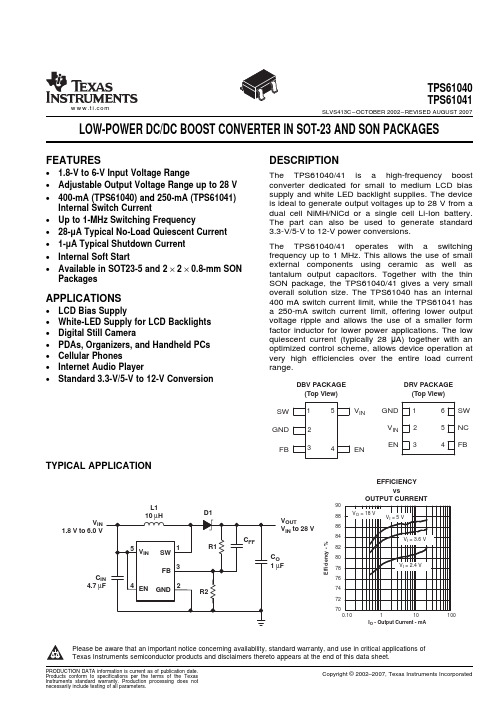
FEATURESDESCRIPTIONAPPLICATIONSDBV PACKAGE (Top View)SW GND FBV INENGND SW V INNC ENFB321456DRV PACKAGE (Top View)TYPICAL APPLICATIONL1D1FV OUTV IN to 28 VV IN1.8 V to 6.0 VC 4.7 µ70727476788082848688900.10110100E f f i c i e n c y - %EFFICIENCYvsOUTPUT CURRENTI O - Output Current - mATPS61040TPS61041SLVS413C–OCTOBER 2002–REVISED AUGUST 2007LOW-POWER DC/DC BOOST CONVERTER IN SOT-23AND SON PACKAGES• 1.8-V to 6-V Input Voltage RangeThe TPS61040/41is a high-frequency boost converter dedicated for small to medium LCD bias •Adjustable Output Voltage Range up to 28V supply and white LED backlight supplies.The device •400-mA (TPS61040)and 250-mA (TPS61041)is ideal to generate output voltages up to 28V from a Internal Switch Currentdual cell NiMH/NiCd or a single cell Li-Ion battery.•Up to 1-MHz Switching FrequencyThe part can also be used to generate standard 3.3-V/5-V to 12-V power conversions.•28-μA Typical No-Load Quiescent Current •1-μA Typical Shutdown Current The TPS61040/41operates with a switching frequency up to 1MHz.This allows the use of small •Internal Soft Startexternal components using ceramic as well as •Available in SOT23-5and 2×2×0.8-mm SON tantalum output capacitors.Together with the thin PackagesSON package,the TPS61040/41gives a very small overall solution size.The TPS61040has an internal 400mA switch current limit,while the TPS61041has •LCD Bias Supplya 250-mA switch current limit,offering lower output voltage ripple and allows the use of a smaller form •White-LED Supply for LCD Backlights factor inductor for lower power applications.The low •Digital Still Cameraquiescent current (typically 28μA)together with an •PDAs,Organizers,and Handheld PCs optimized control scheme,allows device operation at •Cellular Phonesvery high efficiencies over the entire load current range.•Internet Audio Player•Standard 3.3-V/5-V to 12-V ConversionPlease be aware that an important notice concerning availability,standard warranty,and use in critical applications of Texas Instruments semiconductor products and disclaimers thereto appears at the end of this data sheet.PRODUCTION DATA information is current as of publication date.Copyright ©2002–2007,Texas Instruments IncorporatedProducts conform to specifications per the terms of the TexasVINFBENTPS61040TPS61041SLVS413C–OCTOBER 2002–REVISED AUGUST 2007These devices have limited built-in ESD protection.The leads should be shorted together or the device placed in conductive foam during storage or handling to prevent electrostatic damage to the MOS gates.ORDERING INFORMATION(1)SWITCH CURRENTPACKAGE T APART NUMBER PACKAGE LIMIT,mAMARKING TPS61040DBV400SOT23-5PHOI TPS61041DBV 250SOT23-5PHPI –40°C to 85°CTPS61040DRV 400SON-62×2CCL TPS61041DRV250SON-62×2CAW(1)The devices are available in tape and reel and in tubes.Add R suffix to the part number (e.g.,TPS61040DRVR)to order quantities of 3000parts in tape and reel or add suffix T (e.g.,TPS61040DRVT)to order a tube with 250pieces..FUNCTIONAL BLOCK DIAGRAM2Submit Documentation Feedback Copyright ©2002–2007,Texas Instruments IncorporatedDETAILED DESCRIPTION OPERATIONPEAK CURRENT CONTROLI peak(typ)+I LIM)V INL100nsI peak(typ)+400mA)V INL100ns for the TPS61040I peak(typ)+250mA)V INL100ns for the TPS61041(1)TPS61040TPS61041SLVS413C–OCTOBER2002–REVISED AUGUST2007 Table1.Terminal FunctionsTERMINALI/O DESCRIPTIONNAME DBV NO.DRV NO.This is the enable pin of the device.Pulling this pin to ground forces the device into shutdownEN43I mode reducing the supply current to less than1μA.This pin should not be left floating and needsto be terminated.This is the feedback pin of the device.Connect this pin to the external voltage divider to program FB34Ithe desired output voltage.GND21–GroundNC–5–No connectionConnect the inductor and the Schottky diode to this pin.This is the switch pin and is connected to SW16Ithe drain of the internal power MOSFET.V IN52I Supply voltage pinThe TPS61040/41operates with an input voltage range of1.8V to6V and can generate output voltages up to 28V.The device operates in a pulse-frequency-modulation(PFM)scheme with constant peak current control. This control scheme maintains high efficiency over the entire load current range,and with a switching frequency up to1MHz,the device enables the use of very small external components.The converter monitors the output voltage,and as soon as the feedback voltage falls below the reference voltage of typically1.233V,the internal switch turns on and the current ramps up.The switch turns off as soon as the inductor current reaches the internally set peak current of typically400mA(TPS61040)or250mA(TPS61041). See the Peak Current Control section for more information.The second criteria that turns off the switch is the maximum on-time of6μs(typical).This is just to limit the maximum on-time of the converter to cover for extreme conditions.As the switch is turned off the external Schottky diode is forward biased delivering the current to the output.The switch remains off for a minimum of400ns(typical),or until the feedback voltage drops below the reference voltage ing this PFM peak current control scheme the converter operates in discontinuous conduction mode(DCM)where the switching frequency depends on the output current,which results in very high efficiency over the entire load current range.This regulation scheme is inherently stable,allowing a wider selection range for the inductor and output capacitor.The internal switch turns on until the inductor current reaches the typical dc current limit(I LIM)of400mA (TPS61040)or250mA(TPS61042).Due to the internal propagation delay of typical100ns,theactualcurrent exceeds the dc current limit threshold by a small amount.The typical peak current limit can be calculated:The higher the input voltage and the lower the inductor value,the greater the peak.By selecting the TPS61040or TPS61041,it is possible to tailor the design to the specific application current limit requirements.A lower current limit supports applications requiring lower output power and allows the use of an inductor with a lower current rating and a smaller form factor.A lower current limit usually has a lower output voltage ripple as well.Copyright©2002–2007,Texas Instruments Incorporated Submit Documentation Feedback3SOFT STARTThe TPS61040/41limits this inrush current by increasing the current limit in two steps starting from I LIM4for 256cycles toI LIM2for the next 256cycles,and then full current limit (see Figure 14).ENABLEUNDERVOLTAGE LOCKOUTABSOLUTE MAXIMUM RATINGSDISSIPATION RATING TABLETPS61040TPS61041SLVS413C–OCTOBER 2002–REVISED AUGUST 2007All inductive step-up converters exhibit high inrush current during start-up if no special precaution is made.This can cause voltage drops at the input rail during start up and may result in an unwanted or early system shut down.Pulling the enable (EN)to ground shuts down the device reducing the shutdown current to 1μA (typical).Because there is a conductive path from the input to the output through the inductor and Schottky diode,the output voltage is equal to the input voltage during shutdown.The enable pin needs to be terminated and should not be left ing a small external transistor disconnects the input from the output during shutdown as shown in Figure 18.An undervoltage lockout prevents misoperation of the device at input voltages below typical 1.5V.When the input voltage is below the undervoltage threshold,the main switch is turned off.over operating free-air temperature (unless otherwise noted)(1)UNIT Supply voltages on pin V IN (2)–0.3V to 7V Voltages on pins EN,FB(2)–0.3V to V IN +0.3VSwitch voltage on pin SW(2)30VContinuous power dissipation See Dissipation Rating TableT J Operating junction temperature –40°C to 150°C T stgStorage temperature–65°C to 150°CLead temperature (soldering 10seconds)260°C(1)Stresses beyond those listed under absolute maximum ratings may cause permanent damage to the device.These are stress ratings only,and functional operation of the device at these or any other conditions beyond those indicated under recommended operating conditions is not implied.Exposure to absolute-maximum-rated conditions for extended periods may affect device reliability.(2)All voltage values are with respect to network ground terminal.DERATING T A ≤25°C FACTOR T A =70°C T A =85°C PACKAGE R θJA POWER RATINGABOVE POWER RATINGPOWER RATINGT A =25°C DBV 250°C/W 357mW 3.5mW/°C 192mW 140mW DRV76°C/W1300mW13mW/°C688mW500mW4Submit Documentation Feedback Copyright ©2002–2007,Texas Instruments IncorporatedRECOMMENDED OPERATING CONDITIONS ELECTRICAL CHARACTERISTICSTPS61040TPS61041 SLVS413C–OCTOBER2002–REVISED AUGUST2007MIN TYP MAX UNITV IN Input voltage range 1.86VV OUT Output voltage range28VL Inductor(1) 2.210μHf Switching frequency(1)1MHzC IN Input capacitor(1) 4.7μFC OUT Output capacitor(1)1μFT A Operating ambient temperature–4085°CT J Operating junction temperature–40125°C (1)See application section for further information.V IN=2.4V,EN=V IN,T A=–40°C to85°C,typical values are at T A=25°C(unless otherwise noted)PARAMETER TEST CONDITIONS MIN TYP MAX UNIT SUPPLY CURRENTV IN Input voltage range 1.86VI Q Operating quiescent current I OUT=0mA,not switching,V FB=1.3V2850μAI SD Shutdown current EN=GND0.11μAV UVLO Under-voltage lockout threshold 1.5 1.7V ENABLEV IH EN high level input voltage 1.3VV IL EN low level input voltage0.4VI I EN input leakage current EN=GND or V IN0.11μA POWER SWITCH AND CURRENT LIMITVsw Maximum switch voltage30Vt off Minimum off time250400550nst on Maximum on time467.5μsR DS(on)MOSFET on-resistance V IN=2.4V;I SW=200mA;TPS610406001000mΩR DS(on)MOSFET on-resistance V IN=2.4V;I SW=200mA;TPS610417501250mΩMOSFET leakage current V SW=28V110μAI LIM MOSFET current limit TPS61040350400450mAI LIM MOSFET current limit TPS61041215250285mA OUTPUTV OUT Adjustable output voltage range V IN28VV ref Internal voltage reference 1.233VI FB Feedback input bias current V FB=1.3V1μAV FB Feedback trip point voltage 1.8V≤V IN≤6V 1.208 1.233 1.258V1.8V≤V IN≤6V;V OUT=18V;I load=10mA;Line regulation(1)0.05%/VC FF=not connectedLoad regulation(1)V IN=2.4V;V OUT=18V;0mA≤I OUT≤30mA0.15%/mA (1)The line and load regulation depend on the external component selection.See the application section for further information.Copyright©2002–2007,Texas Instruments Incorporated Submit Documentation Feedback5TYPICAL CHARACTERISTICS70727476788082848688900.10110100E f f i c i e n c y - %I O - Output Current - mA70727476788082848688900.10110100E f f i c i e n c y - %I L - Load Current - mATPS61040TPS61041SLVS413C–OCTOBER 2002–REVISED AUGUST 2007Table 2.Table of GraphsFIGUREvs Load current 1,2,3ηEfficiency vs Input voltage4I Q Quiescent current vs Input voltage and temperature 5V FB Feedback voltage vs Temperature 6I SW Switch current limit vs Temperature7vs Supply voltage,TPS610418I CL Switch current limit vs Supply voltage,TPS610409vs Temperature 10R DS(on)R DS(on)vs Supply voltage11Line transient response 12Load transient response 13Start-up behavior14EFFICIENCYEFFICIENCYvsvsOUTPUT CURRENTLOAD CURRENTFigure 1.Figure 2.6Submit Documentation Feedback Copyright ©2002–2007,Texas Instruments Incorporated70727476788082848688900.10110100E f f i c i e n c y - %I L - Load Current - mA123456E f f i c i e n c y - %V I - Input Voltage - V- F e e d b a c k V o l t a g e - VV F B T A - Temperature - °CQ u i e s c e n t C u r r e n t - AµV I - Input Voltage - VTPS61040TPS61041SLVS413C–OCTOBER 2002–REVISED AUGUST 2007EFFICIENCYEFFICIENCYvsvsLOAD CURRENT INPUT VOLTAGEFigure 3.Figure 4.TPS61040QUIESCENT CURRENTFEEDBACK VOLTAGEvsvsFigure 5.Figure 6.Copyright ©2002–2007,Texas Instruments Incorporated Submit Documentation Feedback 7T A - Temperature - °CI (S W )- S w i t c h C u r r e n t L i m i t - m A- C u r r e n t L i m i t - m AI (C L ) V CC - Supply Voltage - VΩr D S (o n )− S t a t i c D r a i n -S o u r c e O n -S t a t e R e s i s t a n c e − m TA − Temperature − °C- C u r r e n t L i m i t - m AI (C L ) V CC - Supply Voltage - VTPS61040TPS61041SLVS413C–OCTOBER 2002–REVISED AUGUST 2007TPS61040/41TPS61041SWITCH CURRENT LIMITCURRENT LIMITvsvsFREE-AIR TEMPERATURE SUPPLY VOLTAGEFigure 7.Figure 8.TPS61040TPS61040/41CURRENT LIMITSTATIC DRAIN-SOURCE ON-STATE RESISTANCEvsvsSUPPLY VOLTAGEFREE-AIR TEMPERATUREFigure 9.Figure 10.8Submit Documentation Feedback Copyright ©2002–2007,Texas Instruments IncorporatedV I2.4 V to3.4 VV O100 mV/div 200 µS/divV O = 18 VΩr D S (o n )− S t a t i c D r a i n -S o u r c e O n -S t a t e R e s i s t a n c e − m V CC − Supply Voltage − VV O 5 V/div EN 1 V/divI I50 mA/divV O = 18 VV O1 mA to 10 mA200 µS/divV O100 mA/divV O = 18 VTPS61040TPS61041SLVS413C–OCTOBER 2002–REVISED AUGUST 2007TPS61040/41STATIC DRAIN-SOURCE ON-STATE RESISTANCEvsFigure 11.Figure 12.Line Transient ResponseFigure 13.Load Transient Tresponse Figure 14.Start-Up BehaviorCopyright ©2002–2007,Texas Instruments Incorporated Submit Documentation Feedback 9APPLICATION INFORMATIONINDUCTOR SELECTION,MAXIMUM LOAD CURRENTfS max +V IN(min) (V OUT *V IN)I P L V OUT (2)fS ǒI load Ǔ+2 I load (V OUT *V IN )Vd)I 2P L(3)I load max +h I 2P L fS max2 (V OUT *VIN)(4)TPS61040TPS61041SLVS413C–OCTOBER 2002–REVISED AUGUST 2007Because the PFM peak current control scheme is inherently stable,the inductor value does not affect the stability of the regulator.The selection of the inductor together with the nominal load current,input and output voltage of the application determines the switching frequency of the converter.Depending on the application,inductor values between 2.2μH and 47μH are recommended.The maximum inductor value is determined by the maximum on time of the switch,typically 6μs.The peak current limit of 400mA/250mA (typically)should be reached within this 6-μs period for proper operation.The inductor value determines the maximum switching frequency of the converter.Therefore,select the inductor value that ensures the maximum switching frequency at the converter maximum load current is not exceeded.The maximum switching frequency is calculated by the following formula:Where:I P =Peak current as described in the Peak Current Control section L =Selected inductor valueV IN(min)=The highest switching frequency occurs at the minimum input voltageIf the selected inductor value does not exceed the maximum switching frequency of the converter,the next stepis to calculate the switching frequency at the nominal load current using the following formula:Where:I P =Peak current as described in the Peak Current Control section L =Selected inductor value I load =Nominal load currentVd =Rectifier diode forward voltage (typically 0.3V)A smaller inductor value gives a higher converter switching frequency,but lowers the efficiency.The inductor value has less effect on the maximum available load current and is only of secondary order.Thebest way to calculate the maximum available load current under certain operating conditions is to estimate the expected converter efficiency at the maximum load current.This number can be taken out of the efficiency graphs shown in Figure 1through Figure 4.The maximum load current can then be estimated as follows:Where:I P =Peak current as described in the Peak Current Control section L =Selected inductor valuefS max =Maximum switching frequency as calculated previously η=Expected converter efficiency.Typically 70%to 85%10Submit Documentation Feedback Copyright ©2002–2007,Texas Instruments IncorporatedSETTING THE OUTPUT VOLTAGEV OUT+1.233Vǒ1)R1R2Ǔ(5)C FF+12p fS20R1(6)TPS61040TPS61041SLVS413C–OCTOBER2002–REVISED AUGUST2007The maximum load current of the conveter is the current at the operation point where the coverter starts to enter the continuous conduction ually the converter should always operate in discontinuous conduction mode.Last,the selected inductor should have a saturation current that meets the maximum peak current of the converter(as calculated in the Peak Current Control section).Use the maximum value for I LIM for this calculation. Another important inductor parameter is the dc resistance.The lower the dc resistance,the higher the efficiency of the converter.See Table3and the typical applications for the inductor selection.Table3.Recommended Inductor for Typical LCD Bias Supply(see Figure15)DEVICE INDUCTOR VALUE COMPONENT SUPPLIER COMMENTS10μH Sumida CR32-100High efficiency10μH Sumida CDRH3D16-100High efficiencyTPS6104010μH Murata LQH4C100K04High efficiency4.7μH Sumida CDRH3D16-4R7Small solution size4.7μH Murata LQH3C4R7M24Small solution sizeHigh efficiencyTPS6104110μH Murata LQH3C100K24Small solution sizeThe output voltage is calculated as:For battery-powered applications,a high-impedance voltage divider should be used with a typical value for R2of ≤200kΩand a maximum value for R1of2.2MΩ.Smaller values might be used to reduce the noise sensitivity of the feedback pin.A feedforward capacitor across the upper feedback resistor R1is required to provide sufficient overdrive for the error comparator.Without a feedforward capacitor,or one whose value is too small,the TPS61040/41shows double pulses or a pulse burst instead of single pulses at the switch node(SW),causing higher output voltage ripple.If this higher output voltage ripple is acceptable,the feedforward capacitor can be left out.The lower the switching frequency of the converter,the larger the feedforward capacitor value required.A good starting point is to use a10-pF feedforward capacitor.As a first estimation,the required value for the feedforward capacitor at the operation point can also be calculated using the following formula:Where:R1=Upper resistor of voltage dividerfS=Switching frequency of the converter at the nominal load current(See the INDUCTOR SELECTION, MAXIMUM LOAD CURRENT section for calculating the switching frequency)C FF=Choose a value that comes closest to the result of the calculationCopyright©2002–2007,Texas Instruments Incorporated Submit Documentation Feedback11 LINE AND LOAD REGULATIONOUTPUT CAPACITOR SELECTIOND V out+I outC outǒ1fS(Iout)–I P LVout)Vd–VinǓ)I P ESR(7)TPS61040TPS61041SLVS413C–OCTOBER2002–REVISED AUGUST2007The larger the feedforward capacitor the worse the line regulation of the device.Therefore,when concern for line regulation is paramount,the selected feedforward capacitor should be as small as possible.See the LINE AND LOAD REGULATION section for more information about line and load regulation.The line regulation of the TPS61040/41depends on the voltage ripple on the feedback ually a50mV peak-to-peak voltage ripple on the feedback pin FB gives good results.Some applications require a very tight line regulation and can only allow a small change in output voltage over a certain input voltage range.If no feedforward capacitor C FF is used across the upper resistor of the voltage feedback divider,the device has the best line regulation.Without the feedforward capacitor the output voltage ripple is higher because the TPS61040/41shows output voltage bursts instead of single pulses on the switch pin (SW),increasing the output voltage ripple.Increasing the output capacitor value reduces the output voltage ripple.If a larger output capacitor value is not an option,a feedforward capacitor C FF can be used as described in the previous section.The use of a feedforward capacitor increases the amount of voltage ripple present on the feedback pin(FB).The greater the voltage ripple on the feedback pin(≥50mV),the worse the line regulation. There are two ways to improve the line regulation further:e a smaller inductor value to increase the switching frequency which will lower the output voltage ripple,as well as the voltage ripple on the feedback pin.2.Add a small capacitor from the feedback pin(FB)to ground to reduce the voltage ripple on the feedback pindown to50mV again.As a starting point,the same capacitor value as selected for the feedforward capacitorC FF can be used.For best output voltage filtering,a low ESR output capacitor is recommended.Ceramic capacitors have a low ESR value but tantalum capacitors can be used as well,depending on the application.Assuming the converter does not show double pulses or pulse bursts on the switch node(SW),the output voltage ripple can be calculated as:where:I P=Peak current as described in the Peak Current Control sectionL=Selected inductor valueI out=Nominal load currentfS(I out)=Switching frequency at the nominal load current as calculated previouslyVd=Rectifier diode forward voltage(typically0.3V)C out=Selected output capacitorESR=Output capacitor ESR valueSee Table4and the typical applications section for choosing the output capacitor.Table4.Recommended Input and Output CapacitorsDEVICE CAPACITOR VOLTAGE RATING COMPONENT SUPPLIER COMMENTS4.7μF/X5R/0805 6.3V Tayo Yuden JMK212BY475MG C IN/C OUT10μF/X5R/0805 6.3V Tayo Yuden JMK212BJ106MG C IN/C OUT TPS61040/411μF/X7R/120625V Tayo Yuden TMK316BJ105KL C OUT1μF/X5R/120635V Tayo Yuden GMK316BJ105KL C OUT4.7μF/X5R/121025V Tayo Yuden TMK325BJ475MG C OUT12Submit Documentation Feedback Copyright©2002–2007,Texas Instruments IncorporatedINPUT CAPACITOR SELECTIONDIODE SELECTIONLAYOUT CONSIDERATIONSD1V OV IN C TPS61040TPS61041SLVS413C–OCTOBER 2002–REVISED AUGUST 2007For good input voltage filtering,low ESR ceramic capacitors are recommended.A 4.7μF ceramic input capacitor is sufficient for most of the applications.For better input voltage filtering this value can be increased.See Table 4and typical applications for input capacitor recommendations.To achieve high efficiency a Schottky diode should be used.The current rating of the diode should meet the peak current rating of the converter as it is calculated in the Peak Current Control e the maximum value for I LIM for this calculation.See Table 5and the typical applications for the selection of the Schottky diode.Table 5.Recommended Schottky Diode for Typical LCD Bias Supply (see Figure 15)DEVICEREVERSE VOLTAGECOMPONENT SUPPLIER COMMENTS30VON Semiconductor MBR053020V ON Semiconductor MBR0520TPS61040/4120V ON Semiconductor MBRM120LHigh efficiency 30VToshiba CRS02Typical for all switching power supplies,the layout is an important step in the design;especially at high peak currents and switching frequencies.If the layout is not carefully done,the regulator might show noise problems and duty cycle jitter.The input capacitor should be placed as close as possible to the input pin for good input voltage filtering.The inductor and diode should be placed as close as possible to the switch pin to minimize the noise coupling into other circuits.Because the feedback pin and network is a high-impedance circuit,the feedback network should be routed away from the inductor.The feedback pin and feedback network should be shielded with a ground plane or trace to minimize noise coupling into this circuit.Wide traces should be used for connections in bold as shown in Figure 15.A star ground connection or ground plane minimizes ground shifts and noise.Figure yout DiagramCopyright ©2002–2007,Texas Instruments Incorporated Submit Documentation Feedback 13L1D1V OUT 18 VV IN1.8 V to 6 VC14.7 µFL1:Sumida CR32-100D1:Motorola MBR0530C1:Tayo Yuden JMK212BY475MG C2:Tayo Yuden TMK316BJ105KLL1D1V IN1.8 V to 6 V4.7 DAC or Analog Voltage 0 V = 25 V 1.233 V = 18 V Sumida CR32-100Motorola MBR0530Tayo Yuden JMK212BY475MG C2:Tayo Yuden GMK316BJ105KLV OUT18 V / 10 mAV IN1.8 V to 6 V4.7 µR3200 k WµF Sumida CR32-100Motorola MBR0530Tayo Yuden JMK212BY475MG Tayo Yuden TMK316BJ105KLTPS61040TPS61041SLVS413C–OCTOBER 2002–REVISED AUGUST 2007Figure 16.LCD Bias SupplyFigure 17.LCD Bias Supply With Adjustable Output VoltageFigure 18.LCD Bias Supply With Load Disconnect14Submit Documentation Feedback Copyright ©2002–2007,Texas Instruments IncorporatedV IN = 2.7 V to 5 VC14.7 µFV2 = -10 V/15 mAMurata LQH4C6R8M04Motorola MBR0530Tayo Yuden JMK212BY475MGTayo Yuden EMK316BJ105KFL1D1µFV O=12 V/35 mAV IN 3.3 V10 µL1:Murata LQH4C6R8M04D1:Motorola MBR0530C1:Tayo Yuden JMK212BJ106MGC2:Tayo Yuden EMK316BJ475MLµF5 V/45 mA1.8 V to 4 V4.7L1:Murata LQH4C3R3M04D1:Motorola MBR0530C1, C2:Tayo Yuden JMK212BY475MGTPS61040TPS61041SLVS413C–OCTOBER2002–REVISED AUGUST2007 Figure19.Positive and Negative Output LCD Bias SupplyFigure20.Standard3.3-V to12-V SupplyFigure21.Dual Battery Cell to5-V/50-mA ConversionEfficiency Approx.Equals84%at V IN=2.4V to Vo=5V/45mACopyright©2002–2007,Texas Instruments Incorporated Submit Documentation Feedback15L1V CCPWM100 Hz to 500 HzL1:Murata LQH4C100K04D1:Motorola MBR0530C1:Tayo Yuden JMK212BY475MG C2:Tayo Yuden TMK316BJ105KLL1D1MBRM120L4.7 µV CC = 2.7 V to 6 V0 V ≅ Iled = 20 mAL1:Murata LQH4C3R3M04D1:Motorola MBR0530C1:Tayo Yuden JMK212BY475MG C2:Standard Ceramic CapacitorTPS61040TPS61041SLVS413C–OCTOBER 2002–REVISED AUGUST 2007Figure 22.White LED Supply With Adjustable Brightness ControlUsing a PWM Signal on the Enable Pin,Efficiency Approx.Equals 86%at V IN =3V,I LED =15mAA.A smaller output capacitor value for C2causes a larger LED ripple.Figure 23.White LED Supply With Adjustable Brightness ControlUsing an Analog Signal on the Feedback Pin16Submit Documentation Feedback Copyright ©2002–2007,Texas Instruments IncorporatedPACKAGING INFORMATIONOrderable Device Status (1)Package Type Package Drawing Pins Package Qty Eco Plan (2)Lead/Ball Finish MSL Peak Temp (3)TPS61040DBVR ACTIVE SOT-23DBV 53000Green (RoHS &no Sb/Br)CU NIPDAU Level-1-260C-UNLIM TPS61040DBVRG4ACTIVE SOT-23DBV 53000Green (RoHS &no Sb/Br)CU NIPDAU Level-1-260C-UNLIM TPS61040DRVR PREVIEW SON DRV 63000TBDCall TI Call TITPS61041DBVR ACTIVE SOT-23DBV 53000Green (RoHS &no Sb/Br)CU NIPDAU Level-1-260C-UNLIM TPS61041DBVRG4ACTIVE SOT-23DBV 53000Green (RoHS &no Sb/Br)CU NIPDAU Level-1-260C-UNLIM TPS61041DRVR PREVIEW SON DRV 53000TBD Call TI Call TI TPS61041DRVTPREVIEWSONDRV5250TBDCall TICall TI(1)The marketing status values are defined as follows:ACTIVE:Product device recommended for new designs.LIFEBUY:TI has announced that the device will be discontinued,and a lifetime-buy period is in effect.NRND:Not recommended for new designs.Device is in production to support existing customers,but TI does not recommend using this part in a new design.PREVIEW:Device has been announced but is not in production.Samples may or may not be available.OBSOLETE:TI has discontinued the production of the device.(2)Eco Plan -The planned eco-friendly classification:Pb-Free (RoHS),Pb-Free (RoHS Exempt),or Green (RoHS &no Sb/Br)-please check /productcontent for the latest availability information and additional product content details.TBD:The Pb-Free/Green conversion plan has not been defined.Pb-Free (RoHS):TI's terms "Lead-Free"or "Pb-Free"mean semiconductor products that are compatible with the current RoHS requirements for all 6substances,including the requirement that lead not exceed 0.1%by weight in homogeneous materials.Where designed to be soldered at high temperatures,TI Pb-Free products are suitable for use in specified lead-free processes.Pb-Free (RoHS Exempt):This component has a RoHS exemption for either 1)lead-based flip-chip solder bumps used between the die and package,or 2)lead-based die adhesive used between the die and leadframe.The component is otherwise considered Pb-Free (RoHS compatible)as defined above.Green (RoHS &no Sb/Br):TI defines "Green"to mean Pb-Free (RoHS compatible),and free of Bromine (Br)and Antimony (Sb)based flame retardants (Br orSb do not exceed 0.1%by weight in homogeneous material)(3)MSL,Peak Temp.--The Moisture Sensitivity Level rating according to the JEDEC industry standard classifications,and peak solder temperature.Important Information and Disclaimer:The information provided on this page represents TI's knowledge and belief as of the date that it is provided.TI bases its knowledge and belief on information provided by third parties,and makes no representation or warranty as to the accuracy of such information.Efforts are underway to better integrate information from third parties.TI has taken and continues to take reasonable steps to provide representative and accurate information but may not have conducted destructive testing or chemical analysis on incoming materials and chemicals.TI and TI suppliers consider certain information to be proprietary,and thus CAS numbers and other limited information may not be available for release.In no event shall TI's liability arising out of such information exceed the total purchase price of the TI part(s)at issue in this document sold by TI to Customer on an annual basis.PACKAGE OPTION ADDENDUM15-Oct-2007。
TPS61032中文资料

MAX UNIT
1.8
5.5 V
-40
85 °C
-40
125 °C
2
元器件交易网
TPS61030 TPS61031, TPS61032
SLUS534D – SEPTEMBER 2002 – REVISED APRIL 2004
ELECTRICAL CHARACTERISTICS
in a TSSOP-16 Package
APPLICATIONS
• All Single Cell Li or Dual Cell Battery Operated Products as MP-3 Player, PDAs, and Other Portable Equipment
DESCRIPTION
These devices have limited built-in ESD protection. The leads should be shorted together or the device placed in conductive foam during storage or handling to prevent electrostatic damage to the MOS gates.
The device is packaged in a 16-pin QFN package measuring 4 mm x 4 mm (RSA) or in a 16-pin TSSOP PowerPAD™ package (PWP).
1.8 V to 5 V
C1
Input 10 µF
L1 6.8 µH
96% EFFICIENT SYNCHRONOUS BOOST CONVERTER WITH 4A SWITCH
Model 6103温度控制器说明书

Complete TerminalAccessories Kit Supplied with Model 6103 for Easy Connections.The 6103 temperature controller with its small size is the logical choice for use on today’smulti-zone extruding and molding machines. It is available off-the-shelf in a wide selection ofthermocouple types and ranges. A complete terminal accessories kit (6100-ACC) is included.6102 Socket Mount Controllerߜ1⁄16DIN Panel Cutout ߜThermocouple and RTDModelsߜTime ProportionalControlߜ10 AMP Capacity ߜ11-Pin Connector6102 Series$145Time ProportionalControl6132 Series$145On/Off ControlThe 6102 is supplied as a complete system with socket.Replacement socketavailable, 6102-SKT ($8)6103 “Space Saver”Panel ControllerߜThermocouple and RTD Models ߜTime Proportional Control ߜ10 AMP Capacity ߜ1⁄4" Terminal LugsShown smaller than actual size.Shown smaller than actual size.6103 Series$149Time Proportional Control1⁄16DIN Temperature ControllersLow Cost Space Saving SystemsThe 6102 temperature controller is one of OMEGA’s lowest cost units with all the features of bigcontrollers. Packaged in a small size to save you space and money, 6102 controllers plug into an unbreakable nylon socket which can be mounted individually or snapped onto the 6000-TRKmounting track. The unbreakable nylon socket and mounting track make installations in chassis, control panel and O.E.M. applications fast and easy, using a minimum of space.1⁄16DIN1⁄16DINP a n e l p u n ch e s a v a i l a b l e , v i s i t o m e g a .c o m/p a n e l p u n c h e sTo order, specify Model No. and range (from chart above.) To order 230V, add suffix “-230V”to model number; no additional charge.Ordering Examples: 6132H-J-0-300C-230V, On/Off Controller with socket mounting and230 Vac power,$145. OCW-3extends standard 3-year warranty to a total of 5 years ($36),$145 + 36 = $181. 6102J-0-1000F, proportional controller with socket mounting,$145. SpecificationsElectricalSupply Voltage:115 Vac(-15% +20%), 50/60 Hz (optional)230 VacPower Consumption:2 VAOutput:10 A relay, SPST with powerinternally wired to contacts; 5 A relay,SPDT for 6132HControlCalibration Accuracy:±2% of scalespan or 4°C, whichever is greater(from 10 to 90% of scale span)Linearity-Resolution:Linearity 6%,resolution 1% max, of scale span(dependent on sensor/range)Control Accuracy:±0.4% of fullscale at an ambient of 22°C (72°F);±2°C (3.6°F), at rated line voltage,after 30 minutes setting time; cycletime: 25 s, approx.Control ModesTime Proportional:Proportional withaccelerated response to temperaturevariations; 3.5% bandOn/Off:Model 6132H only;4°C (7°F) differentialInputThermocouple: J, K, SExternal resistance:Max 100 ΩCold Junction Compensation:AutomaticCommon Mode:Negligible effect upto 270V 50/60 HzSeries Mode:Negligible effectup to scale spread mV equivalent at50/60 HzSensor Break Protection:Automatic upscaleRTD Sensor: 100 Ω platinum␣=0.00385GeneralIndication: A high brightness LEDshows Heat ONAmbient Temperature: 0 to 50°C(32 to 122°F)Suppression:Filtering is provided forline and sensor input interferenceDimensions: 48 H x 48 W x 98 mm D(1.89 x 1.89 x 3.86")Construction: Flame retardantpolycarbonate and ABS.Bezel and knob coated with NextelConnections: 6 mm (1⁄4") standardterminal lugs or 11-pin connectorWeight: 200 g (7 oz)DIN panel cutout(1.97)45 (1.8)squareOMEGACARE SM extendedwarranty program is available formodels shown on this page. Askyour sales representative for fulldetails when placing an order.OMEGACARE SM covers parts,labor, and equivalent loaners.Track MountingMounting track is available in 3-foot sections,6000-TRK, $8.50CANADA www.omega.ca Laval(Quebec) 1-800-TC-OMEGA UNITED KINGDOM www. Manchester, England0800-488-488GERMANY www.omega.deDeckenpfronn, Germany************FRANCE www.omega.fr Guyancourt, France088-466-342BENELUX www.omega.nl Amstelveen, NL 0800-099-33-44UNITED STATES 1-800-TC-OMEGA Stamford, CT.CZECH REPUBLIC www.omegaeng.cz Karviná, Czech Republic596-311-899TemperatureCalibrators, Connectors, General Test and MeasurementInstruments, Glass Bulb Thermometers, Handheld Instruments for Temperature Measurement, Ice Point References,Indicating Labels, Crayons, Cements and Lacquers, Infrared Temperature Measurement Instruments, Recorders Relative Humidity Measurement Instruments, RTD Probes, Elements and Assemblies, Temperature & Process Meters, Timers and Counters, Temperature and Process Controllers and Power Switching Devices, Thermistor Elements, Probes andAssemblies,Thermocouples Thermowells and Head and Well Assemblies, Transmitters, WirePressure, Strain and ForceDisplacement Transducers, Dynamic Measurement Force Sensors, Instrumentation for Pressure and Strain Measurements, Load Cells, Pressure Gauges, PressureReference Section, Pressure Switches, Pressure Transducers, Proximity Transducers, Regulators,Strain Gages, Torque Transducers, ValvespH and ConductivityConductivity Instrumentation, Dissolved OxygenInstrumentation, Environmental Instrumentation, pH Electrodes and Instruments, Water and Soil Analysis InstrumentationHeatersBand Heaters, Cartridge Heaters, Circulation Heaters, Comfort Heaters, Controllers, Meters and SwitchingDevices, Flexible Heaters, General Test and Measurement Instruments, Heater Hook-up Wire, Heating Cable Systems, Immersion Heaters, Process Air and Duct, Heaters, Radiant Heaters, Strip Heaters, Tubular HeatersFlow and LevelAir Velocity Indicators, Doppler Flowmeters, LevelMeasurement, Magnetic Flowmeters, Mass Flowmeters,Pitot Tubes, Pumps, Rotameters, Turbine and Paddle Wheel Flowmeters, Ultrasonic Flowmeters, Valves, Variable Area Flowmeters, Vortex Shedding FlowmetersData AcquisitionAuto-Dialers and Alarm Monitoring Systems, Communication Products and Converters, Data Acquisition and Analysis Software, Data LoggersPlug-in Cards, Signal Conditioners, USB, RS232, RS485 and Parallel Port Data Acquisition Systems, Wireless Transmitters and Receivers。
XC6103B544资料
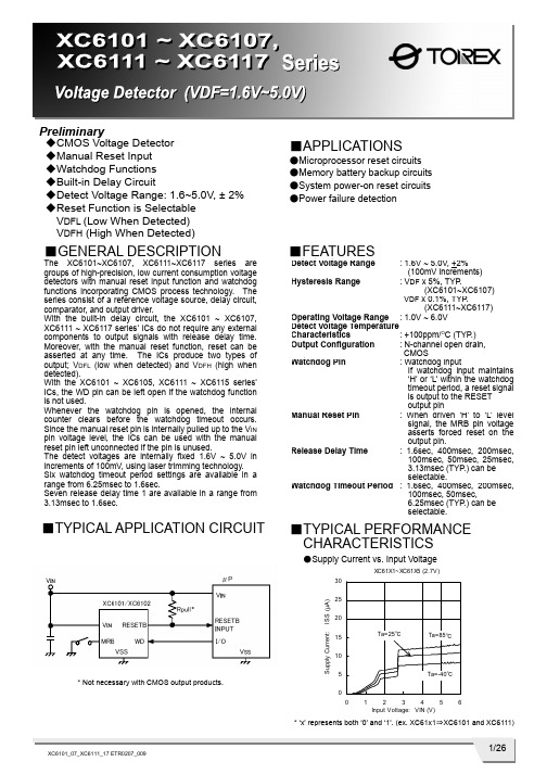
1/26XC6101_07_XC6111_17 ETR0207_009Preliminary◆CMOS Voltage Detector◆Manual Reset Input ◆Watchdog Functions ◆Built-in Delay Circuit ◆Detect Voltage Range: 1.6~5.0V, ± 2% ◆Reset Function is Selectable V DFL (Low When Detected) V DFH (High When Detected)■GENERAL DESCRIPTION The XC6101~XC6107, XC6111~XC6117 series aregroups of high-precision, low current consumption voltage detectors with manual reset input function and watchdog functions incorporating CMOS process technology. The series consist of a reference voltage source, delay circuit, comparator, and output driver.With the built-in delay circuit, the XC6101 ~ XC6107, XC6111 ~ XC6117 series’ ICs do not require any external components to output signals with release delay time. Moreover, with the manual reset function, reset can be asserted at any time. The ICs produce two types of output; V DFL (low when detected) and V DFH (high when detected).With the XC6101 ~ XC6105, XC6111 ~ XC6115 series’ ICs, the WD pin can be left open if the watchdog function is not used. Whenever the watchdog pin is opened, the internal counter clears before the watchdog timeout occurs. Since the manual reset pin is internally pulled up to the V IN pin voltage level, the ICs can be used with the manual reset pin left unconnected if the pin is unused.The detect voltages are internally fixed 1.6V ~ 5.0V in increments of 100mV, using laser trimming technology. Six watchdog timeout period settings are available in a range from 6.25msec to 1.6sec. Seven release delay time 1 are available in a range from 3.13msec to 1.6sec.■APPLICATIONS●Microprocessor reset circuits●Memory battery backup circuits ●System power-on reset circuits ●Power failure detection■TYPICAL APPLICATION CIRCUIT* Not necessary with CMOS output products.■FEATURESDetect Voltage Range: 1.6V ~ 5.0V, +2% (100mV increments)Hysteresis Range : V DF x 5%, TYP .(XC6101~XC6107)V DF x 0.1%, TYP .(XC6111~XC6117)Operating Voltage Range : 1.0V ~ 6.0V Detect Voltage Temperature Characteristics : +100ppm/O C (TYP .) Output Configuration : N-channel open drain,CMOSWatchdog Pin : Watchdog inputIf watchdog input maintains ‘H’ or ‘L’ within the watchdog timeout period, a reset signal is output to the RESET output pinManual Reset Pin : When driven ‘H’ to ‘L’levelsignal, the MRB pin voltage asserts forced reset on theoutput pin.Release Delay Time : 1.6sec, 400msec, 200msec,100msec, 50msec, 25msec, 3.13msec (TYP .) can be selectable.Watchdog Timeout Period : 1.6sec, 400msec, 200msec,100msec, 50msec,6.25msec (TYP .) can be selectable.■TYPICAL PERFORMANCE CHARACTERISTICS ●Supply Current vs. Input Voltage* ‘x’ represents both ‘0’ and ‘1’. (ex. XC61x1⇒XC6101 and XC6111)2/26XC6101~XC6107, XC6111~XC6117 SeriesPIN NUMBERXC6101, XC6102 XC6103 XC6104, XC6105XC6106, XC6107XC6111, XC6112 XC6113 XC6114, XC6115XC6116, XC6117SOT-25 USP-6C SOT-25 USP-6C SOT-25 USP-6C SOT-25USP-6CPIN NAMEFUNCTION1 4 - - 1 4 1 4 R ESETB Reset Output(V DFL : Low Level When Detected)2 5 2 5 2 5 2 5 V SSGround3 2 3 2 - -4 1 M RB ManualReset 4 1 4 1 4 1 - - WDWatchdog5 6 5 6 5 6 5 6 V IN Power Input - - 1 4 3 2 3 2 RESETReset Output (V DFH: High Level When Detected)■PIN CONFIGURATION SOT-25 (TOP VIEW)MRBV IN WD RESETBV SSMRBWD RESETV SSV IN RESETWD RESETBV SS V IN SOT-25 (TOP VIEW)RESETMRB RESETBV SS V IN SOT-25 (TOP VIEW) ■PIN ASSIGNMENT●SOT-25XC6101, XC6102 SeriesXC6111, XC6112 SeriesSOT-25 (TOP VIEW)XC6103 & XC6113 SeriesXC6104, XC6105 Series XC6114, XC6115 SeriesXC6106, XC6107 Series XC6116, XC6117 Series●USP-6CXC6101, XC6102 Series XC6111, XC6112 SeriesXC6103 & XC6113 SeriesXC6104, XC6105 Series XC6114, XC6115 SeriesXC6106, XC6107 Series XC6116, XC6117 SeriesUSP-6C (BOTTOM VIEW)USP-6C (BOTTOM VIEW)USP-6C (BOTTOM VIEW)USP-6C (BOTTOM VIEW)* The dissipation pad for the USP-6C package should be solder-plated in recommended mount pattern and metal masking so as to enhance mounting strength and heat release. If the pad needs to be connected to other pins, it should be connected to the V SS pin.3/26XC6101 ~ XC6107, XC6111~ XC6117SeriesRESET OUTPUTSERIES WATCHDOGMANUAL RESET V DFL (RESETB)V DFH (RESET)XC6101 XC6111 Available Available CMOS - XC6102XC6112AvailableAvailableN-channel open drain-XC6103 XC6113 Available Available - CMOS XC6104 XC6114 Available Not AvailableCMOS CMOS XC6105 XC6115 Available Not Available N-channel open drain CMOS XC6106 XC6116 Not Available AvailableCMOSCMOS XC6107XC6117Not AvailableAvailableN-channel open drainCMOSDESIGNATORDESCRIPTIONSYMBOLDESCRIPTION0 : V DF x 5% (TYP .) with hysteresis ① Hysteresis Range1 : V DF x 0.1% (TYP .) without hysteresis② Functions and Type of Reset Output1 ~ 7: Watchdog and manual functions, and reset output type as per Selection Guide in the above chartA : 3.13msec (TYP .)B : 25msec (TYP .) C: 50msec (TYP .) D : 100msec (TYP .) E : 200msec (TYP .) F : 400msec (TYP .) ③ Release Delay Time * H : 1.6sec (TYP .)0 : No WD timeout period forXC6106, XC6107, XC6116, XC6117 Series 1: 6.25msec (TYP .) 2 : 50msec (TYP .) 3 : 100msec (TYP .) 4 : 200msec (TYP .) 5 : 400msec (TYP .) ④ Watchdog Timeout Period6: 1.6sec (TYP .) ⑤⑥ Detect Voltage 16 ~ 50: Detect voltageex.) 4.5V: ⑤⇒4, ⑥⇒5M : SOT-25 ⑦ Package E : USP-6C R : Embossed tape, standard feed ⑧ Device OrientationL: Embossed tape, reverse feed* Please set the release delay time shorter than or equal to the watchdog timeout period. ex.) XC6101D427MR or XC6101D327MR■PRODUCT CLASSIFICATION ●Selection Guide ●Ordering Information XC61①②③④⑤⑥⑦⑧4/26XC6101~XC6107, XC6111~XC6117 Series■PACKAGING INFORMATION●SOT-25●USP-6C5/26XC6101 ~ XC6107, XC6111~ XC6117Series④ Represents production lot number0 to 9 and A to Z and inverted 0 to 9 and A to Z repeated. (G, I, J, O, Q, W expected.) * ‘X’ represents both ‘0’ and ‘1’. (ex. XC61X1⇒XC6101 and XC6111)■MARKING RULE●SOT-25①②③④SOT-25 (TOP VIEW)6/26XC6101~XC6107, XC6111~XC6117 Series① Represents product series② Represents release delay time MARK RELEASE DELAY TIME PRODUCT SERIES A 3.13msec XC61XxAxxxxx B 25msec XC61XxBxxxxx C 50msec XC61XxCxxxxx D 100msec XC61XxDxxxxx E 200msec XC61XxExxxxx F 400msec XC61XxFxxxxx H 1.6sec XC61XxHxxxxx③ Represents watchdog timeout period MARK WATCHDOG TIMEOUT PERIOD PRODUCT SERIES 0 XC61X6, XC61X7 series XC61Xxx0xxxx 1 6.25msec XC61Xxx1xxxx 2 50msec XC61Xxx2xxxx 3 100msec XC61Xxx3xxxx 4 200msec XC61Xxx4xxxx 5 400msec XC61Xxx5xxxx 6 1.6sec XC61Xxx6xxxx④⑤ Represents detect voltage MARK④ ⑤DETECT VOLTAGE (V)PRODUCT SERIES3 3 3.3 XC61Xxxx33xx 5 0 5.0XC61Xxxx50xx⑥ Represents production lot number0 to 9 and A to Z repeated. (G, I, J, O, Q, W excepted.)* No character inversion used. ** ‘X’ represents both ‘0’ and ‘1’. (ex. XC61X1⇒XC6101 and XC6111)MARK PRODUCT SERIES MARK PRODUCT SERIES 3 XC6101xxxxxx 8 XC6111xxxxxx 4 XC6102xxxxxx 9 XC6112xxxxxx 5 XC6103xxxxxx A XC6113xxxxxx 6 XC6104xxxxxx B XC6114xxxxxx 7 XC6105xxxxxx C XC6115xxxxxx 3 XC6106xxxxxx 8 XC6116xxxxxx 4 XC6107xxxxxx 9 XC6117xxxxxx■MARKING RULE (Continued)●USP-6CUSP-6C (TOP VIEW)7/26XC6101 ~ XC6107, XC6111~ XC6117Series■BLOCK DIAGRAMS●XC6101, XC6111 Series●XC6102, XC6112 Series●XC6103, XC6113 Series8/26XC6101~XC6107, XC6111~XC6117 Series■BLOCK DIAGRAMS (Continued)●XC6107, XC6117 Series●XC6106, XC6116 Series●XC6105, XC6115 Series●XC6104, XC6114 Series9/26XC6101 ~ XC6107, XC6111~ XC6117SeriesPARAMETERSYMBOL RATINGSUNITSV INV SS -0.3 ~ 7.0 VM RBV SS -0.3 ~ V IN +0.3 VInput Voltage WD V SS -0.3 ~ 7.0V Output Current I OUT 20 mACMOS Output RESETB/RESET V SS -0.3 ~ V IN +0.3Output Voltage N-ch Open Drain Output RESETB V SS -0.3 ~ 7.0VSOT-25 250Power Dissipation USP-6C Pd 100mWOperational Temperature Range Topr -40 ~ +85 OCStorage Temperature Range Tstg -40 ~ +125 OC■ABSOLUTE MAXIMUM RATINGSTa = 25O C10/26XC6101~XC6107, XC6111~XC6117 SeriesNOTE:*1: XC6101~XC6107 (with hysteresis) *2: XC6111~XC6117 (without hysteresis)*3: ‘X’ represents both ‘0’ and ‘1’. (ex. XC61X1⇒XC6101 and XC6111) *4: V DF(T): Setting detect voltage*5: If only “V DF ” is indicated, it represents both V DFL (low when detected) and V DFH (high when detected).PARAMETERSYMBOLCONDITIONSMIN.TYP .MAX. UNITS CIRCUITDetect Voltage V DFL V DFHV DF(T)× 0.98V DF(T) V DF(T)× 1.02 V 1 Hysteresis Range XC6101~XC6107 (*1) V HYS V DF × 0.02V DF × 0.05 V DF× 0.08 V 1Hysteresis Range XC6111~XC6117 (*2) V HYS 0 V DF × 0.001 V DFx 0.01V 1V IN =V DF(T)×0.9V - 5 11 V IN =V DF(T)×1.1V- 10 16 XC61X1/XC61X2/XC61X3XC61X4/XC61X5 (*3)(The MRB & the WD Pin: No connection) V IN =6.0V - 1218 V IN =V DF(T)×0.9V - 4 10 V IN =V DF(T)×1.1V - 8 14 Supply Current I SS XC61X6/XC61X7 (*3)(The MRB Pin: No connection)V IN = 6.0V - 1016 µA 2Operating Voltage V IN 1.0 - 6.0 V 1VIN = 1.0V 0.15 0.5 -V IN =2.0V (V DFL(T)> 2.0V) 2.0 2.5 - V IN =3.0V (V DFL(T) >3.0V) 3.0 3.5 -N-ch.V DS = 0.5V V IN =4.0V (V DFL(T) >4.0V) 3.5 4.0 - 3 V DFL Output Current (RESETB) I RBOUTCMOS,P-chV DS = 0.5V V IN = 6.0V - - 1.1 -0.8 mA 4 N-chV DS = 0.5VV IN =6.0V 4.4 4.9 - 3V IN =1.0V - - 0.08 - 0.02 V IN =2.0V (V DFH(T)> 2.0V)- - 0.50 - 0.30 V IN =3.0V (V DFH(T)>3.0V)- - 0.75 - 0.55V DFHOutput Current (RESET) I ROUT P-ch. V DS = 0.5V V IN =4.0V (V DFH(T)>4.0V)- - 0.95 - 0.75 mA 4Temperature Characteristics △V DF / △Topr ・V DF -40OC < Topr < 85 O C - +100 - ppm / O C12 3.13 5 13 25 3825 50 75 60 100 140 120 200 280 240 400 560Release Delay Time(V DF <1.8V)T DR Time until V IN is increased from1.0V to2.0Vand attains to the release time level,and the Reset output pin inverts.960 1600 2240 ms 5 2 3.13 5 13 25 38 25 50 7560 100 140 120 200 280 240 400 560 Release Delay Time(V DF >1.9V)T DRTime until V IN is increased from1.0V to (V DF x1.1V) and attains to the releasetime level,and the Reset output pin inverts. 960 1600 2240ms 5 Detect Delay Time T DFTime until V IN is decreased from 6.0V to 1.0V and attains to the detect voltage level, and the Reset output pin detectswhile the WD pin left opened.- 3 30 µs 5V DFL /V DFH CMOS Output Leak CurrentI LEAK V IN =6.0V, RESETB=6.0V (V DFL ) V IN =6.0V, RESET=0V (V DFH )- 0.01 - µA 3V DFL N-ch Open DrainOutput Leak CurrentI LEAKV IN =6.0V, RESETB=6.0V-0.010.10µA 3■ELECTRICAL CHARACTERISTICS●XC6101~XC6107, XC6111~XC6117 SeriesTa = 25O CSeriesPARAMETERSYMBOL CONDITIONS MIN.TYP . MAX. UNITS CIRCUIT3.13 6.25 9.38 25 50 7560 100 140 120 200 280240 400 560 Watchdog Timeout Period (V DF <1.8V)T WDTime until V IN increases form1.0V to2.0V andthe Reset output pin is released to go into the detection state. (WD=V SS )960 1600 2240 ms 6 3.13 6.25 9.38 25 50 75 60 100 140 120 200 280240 400 560 Watchdog Timeout Period (V DF >1.9V)T WDTime until V IN increases form1.0V to (V DF x1.1V)and the Reset output pin is released to go into the detection state. (WD=V SS )960 1600 2240 ms 6 WatchdogMinimum Pulse Width T WDIN V IN =6.0V,Apply pulse from 6.0V to 0Vto the WD pin. 300 - - ns 7 Watchdog High Level VoltageV WDH V IN =V DF x 1.1V ~ 6.0V V IN x 0.7- 6 V 7 Watchdog Low Level Voltage V WDL V IN =V DF x 1.1V ~ 6.0V0 - V IN x 0.3 V 7 V IN =6.0V, V WD =6.0V (Avg. when peak )- 12 19Watchdog Input Current I WD V IN =6.0V, V WD =0V (Avg. when peak) - 19 -12 -µA 8 Watchdog Input ResistanceR WDV IN =6.0V, V WD =0V, R WD =V IN / |I WD |315500880k Ω8PARAMETERSYMBOL CONDITIONS MIN.TYP . MAX.UNITS CIRCUITMRBHigh Level VoltageV MRH V IN =V DF x1.1V ~ 6.0V 1.4 - V IN 9MRBLow Level VoltageV MRL V IN =V DF x1.1V ~ 6.0V-0.35 V9MRBPull-up Resistance R MR V IN =6.0V, MRB=0V, R MR =V IN / |I MRB | 1.6 2.4 3.0 M Ω 10 MRB Minimum Pulse Width (*3) XC6101~XC6105 XC6111~XC6115 T MRINV IN =6.0V,Apply pulse from 6.0V to 0V tothe MRB pin 2.8 - -MRB Minimum Pulse Width (*4) XC6106, XC6107 XC6116, XC6117T MRIN V IN =6.0V,Apply pulse from 6.0V to 0V tothe MRB pin1.2 - -µs11●XC6101 ~ XC6103, XC6106 ~ XC6107, XC6111 ~ XC6113, XC6116 ~ XC6117 Series NOTE:*1: V DF(T): Setting detect voltage *2: If only “V DF ” is indicated, it represents both V DFL (low when detected) and V DFH (high when detected). *3: Watchdog function is available. *4: Watchdog function is not available.Ta = 25O CTa = 25O C ■ELECTRICAL CHARACTERISTICS (Continued)●XC6101~XC6105, XC6111~XC6115 Series■OPERATIONAL EXPLANATIONThe XC6101~XC6107, XC6111~XC6117 series compare, using the error amplifier, the voltage of the internal voltage reference source with the voltage divided by R1, R2 and R3 connected to the V IN pin. The resulting output signal from the error amplifier activates the watchdog logic, manual reset logic, delay circuit and the output driver. When the V IN pin voltage gradually falls and finally reaches the detect voltage, the RESETB pin output goes from high to low in the case of the V DFL type ICs, and the RESET pin output goes from low to high in the case of the V DFH type ICs.<RESETB / RESET Pin Output Signal>* V DFL (RESETB) type - output signal: Low when detected.The RESETB pin output goes from high to low whenever the V IN pin voltage falls below the detect voltage, or whenever the MRB pin is driven from high to low. The RESETB pin remains low for the release delay time (T DR) after the V IN pin voltage reaches the release voltage. If neither rising nor falling signals are applied to the WD pin within the watchdog timeout period, the RESETB pin output remains low for the release delay time (T DR), and thereafter the RESET pin outputs high level signal. * V DFH (RESET) type – output signal: High when detected.The RESET pin output goes from low to high whenever the V IN pin voltage falls below the detect voltage, or whenever the MRB pin is driven from high to low. The RESET pin remains high for the release delay time (T DR) after the V IN pin voltage reaches the release voltage. If neither rising nor falling signals are applied to the WD pin within the watchdog timeout period, the V OUT pin output remains high for the release delay time (T DR), and thereafter the RESET pin outputs low level signal.<Hysteresis>When the internal comparator output is high, the NMOS transistor connected in parallel to R3 is turned ON, activating the hysteresis circuit. The difference between the release and detect voltages represents the hysteresis range, as shown by the following calculations:V DF (detect voltage) = (R1+R2+R3) x Vref(R2+R3)V DR (release voltage) = (R1+R2) x Vref(R2)V HYS (hysteresis range)=V DR-V DF (V)V DR > V DF* Detect voltage (V DF) includes conditions of both V DFL (low when detected) and V DFH (high when detected).* Please refer to the block diagrams for R1, R2, R3 and Vref.Hysteresis range is selectable from V DF x 0.05V (XC6101~XC6107) or V DF x 0.001V (XC6111~XC6117).<Watchdog (WD) Pin>The XC6101~XC6107, XC6111~XC6117 series use a watchdog timer to detect malfunction or “runaway” of the microprocessor. If neither rising nor falling signals are applied from the microprocessor within the watchdog timeout period, the RESETB/RESET pin output maintains the detection state for the release delay time (T DR), and thereafter the RESET/RESETB pin output returns to the release state (Please refer to the FUNCTION CHART). The timer in the watchdog is then restarted. Six watchdog timeout period settings are available in 1.6sec, 400msec, 200msec, 100msec, 50msec, 6.25msec.<MRB Pin>Using the MRB pin input, the RESET/RESETB pin signal can be forced to the detection state. When the MRB pin is driven from high to low, the RESETB pin output goes from high to low in the case of the V DFL type ICs, and the RESET pin output goes from low to high in the case of the V DFH type. Even after the MRB pin is driven back high, the RESET/RESETB pin output maintains the detection state for the release delay time (T DR). Since the MRB pin is internally pulled up to the V IN pin voltage level, leave the MRB pin open if unused (Please refer to the FUNCTION CHART). A diode, which is an input protection element, is connected between the MRB pin and V IN pin. Therefore, if the MRB pin is applied voltage that exceeds V IN, the current will flow to V IN through the diode. Please use this IC within the stated maximum ratings (V SS -0.3 ~ V IN+0.3) on the MRB pin.<Release Delay Time>Release delay time (T DR) is the time that elapses from when the V IN pin reaches the release voltage, or when the watchdog timeout period expires with no rising signal applied to the WD pin, until the RESET/RESETB pin output is released from the detection state. Seven release delay time (T DR) watchdog timeout period settings are available in 1.6sec, 400msec, 200msec, 100msec, 50msec, 25msec, 3.13msec.<Detect Delay Time>Detect Delay Time (T DF) is the time that elapses from when the V IN pin voltage falls to the detect voltage until the RESET/ RESETB pin output goes into the detection state.Series■TIMING CHARTS●CMOS Output●T DF (CMOS Output)VINVDFL LevelGNDVIN Level VDFL Level GNDVIN x 0.1V■NOTES ON USE1. Please use this IC within the stated maximum ratings. Operation beyond these limits may cause degrading or permanent damage to the device.2. When a resistor is connected between the V IN pin and the input, the V IN voltage drops while the IC is operating and a malfunction may occur as a result of the IC’s through current. For the CMOS output products, the V IN voltage drops while the IC is operating and malfunction may occur as a result of the IC’s output current. Please be careful with using the XC6111~XC6117 series (without hysteresis).3. In order to stabilize the IC’s operations, please ensure that the V IN pin’s input frequency’s rise and fall times are more than 1 µ sec/V.4. Noise at the power supply may cause a malfunction of the watchdog operation or the circuit. In such case, please strength the line between V IN and the GND pin and connect about 0.22µF of a capacitor between the V IN pin and the GND pin.5. Protecting against a malfunction while the watchdog time out period, an ignoring time (no reaction time) occurs to the rise and fall times. Referring to the figure below, the ignoring time (no reaction time) lasts for 900µsec at maximum.GNDGNDGNDVIN Pin Wave FormWD Pin Wave FormRESETB Pin Wave Form (VDFL)SeriesPIN NAMELOGIC CONDITIONSH V IN >V DF +V HYS V IN L V IN <V DF H MRB>1.40V MRBL MRB<0.35V H When keeping W D >V WDH more than T WD L When keeping W D <V WDL more than T WD L → H V WDL → V WDH , T WDIN >300nsec WDH → L V WDH →V WDH , T WDIN >300nsecV IN MRB WD RESETB (*2) H HH LRepeat detect and release (H →L →H)H OpenH L → HH H or Open H → L H HLL *1 LV IN MRB WD RESETB (*3) H HH LRepeat detect and release (L →H →L)H OpenH L → HH H or Open H → L L HLL *1 HV IN WD RESETB (*2) RESET (*3) H HH L Repeat detect and release (H →L →H)Repeat detect and release (L →H →L)H OpenH L → HH H → L H L HL*1 L HV IN MRB RESETB (*2)RESET (*3)H H or Open H LH LL L H■PIN LOGIC CONDITIONSNOTE:*1: If only “V DF ” is indicated, it represents both V DFL (low when detected) and V DFH (high when detected).*2: For the details of each parameter, please see the electrical characteristics. V DF : Detect VoltageV HYS : Hysteresis RangeV WDH : WD High Level Voltage V WDL: WD Low Level Voltage T WDIN : WD Pulse Width T WD : WD Timeout Period■FUNCTION CHART●XC6103/XC61113 Series●XC6104/XC61114, XC6105/XC6115 Series●XC6106/XC61116, XC6107/XC6117 Series●XC6101/XC61111, XC6102/6112 Series*1: Including all logic of WD (WD=H, L, L →H, H →L, OPEN). *2: When the RESETB is High, the circuit is in the release state. When the RESETB is Low, the circuit is in the detection state. *3: When the RESET is High, the circuit is in the release state. When the RESET is Low, the circuit is in the detection state.■TEST CIRCUITSCircuit 1Circuit 2Circuit 3Circuit 4Series ■TEST CIRCUITS (Continued)Circuit 5Circuit 6Circuit 7■TEST CIRCUITS (Continued)Circuit 8Circuit 9Circuit 10Circuit 11Series■TYPICAL PERFORMANCE CHARACTERISTICS(1.1) Supply Current vs. Input Voltage(1.2) Supply Current vs. Input Voltage■TYPICAL PERFORMANCE CHARACTERISTICS (Continued)(2) Detect, Release Voltage vs. Ambient Temperature(1.2) Supply Current vs. Input Voltage (Continued)Series■TYPICAL PERFORMANCE CHARACTERISTICS (Continued) (3-1) Output Voltage vs. Input Voltage (V DFL ) (3.1) Detect, Release Voltage vs. Input Voltage (V DFL )(3.2) Detect, Release Voltage vs. Input Voltage (V DFH )■TYPICAL PERFORMANCE CHARACTERISTICS (Continued)(4) N-ch Driver Output Current vs. V DSSeries(6) P-ch Driver Output Current vs. Input Voltage 1■TYPICAL PERFORMANCE CHARACTERISTICS (Continued)(8) Release Delay Time vs. Ambient Temperature(7) P-ch Driver Output Current vs. Input Voltage 2■TYPICAL PERFORMANCE CHARACTERISTICS (Continued) (10) Release Delay Time vs. Input Voltage(11) Watchdog Timeout Period vs. Input VoltageSeries■TYPICAL PERFORMANCE CHARACTERISTICS (Continued)(14) MRB Low Level Voltage vs. Ambient Temperature(15) MRB High Level Voltage vs. Ambient Temperature* ‘X’ represents both ‘0’ and ‘1’. (ex. XC61X1⇒XC6101 and XC6111)。
API610标准的机械密封材料与分类编码
API610标准的机械密封材料与分类编码API 610标准的机械密封材料与分类编码机械密封的材料与结构特点,务必根据下列分类系统来编码:第一位字母:平衡型(B)或者不平衡型(U)第二位字母:单端面(S),无压的双重密封(T)——即第7版中称“串联密封”,或者有压的双重密封(D)——即第7版中称“双端面密封”第三位字母:密封板(即密封压盖)型式:P=普通式,不带节流衬套;T=节流衬套式,设有急冷、泄漏液接收孔与(或者)排液接孔;A=辅助密封装置,型号需要加以规定。
第四位字母:垫(密封环)材料(见表1)第五位字母:端面材料(见表2)举例来说:一种编码为BSTFM的密封,就是一种平衡型、单端面的、装有带节流衬套的密封板的机械密封,静密封环垫材料为氟橡胶(FKM),动密封环与轴套之间的垫为氟橡胶(FKM),动静环端面副材料为碳对2型碳化钨,对以上材料以外的密封材料应当编码为X,并应在数据单上明确规定之。
机械密封的注解:1、除非另有规定,使用多弹簧密封的弹簧材料务必使用哈斯特洛伊合金(Hastelloy C)。
单弹簧密封的弹簧材料务必使用奥氏体不锈钢(AISI标准型316或者同等材料)。
其它金属零件也务必使用奥氏体不锈钢(AISI标准型316或者同等材料)或者适用于使用条件的其它耐腐蚀材料,但对金属波纹管除外,假如使用金属波纹管,其材料务必由密封制造厂根据使用条件推荐,金属波纹管的腐蚀速率应低于每年50μm(2mils,密耳)。
2、除非另有规定,密封板(即密封压盖)与密封室之间的密封应当使用氟橡胶的O形环,其使用温度低于150℃(300°F)。
假如温度超过150℃以上或者假如有规定,务必使用石墨充填的奥氏体不锈钢蜗形缠绕垫,此蜗形缠绕垫务必能够承受泵送液体的全温(即未采取冷却降温的)。
3、金属密封环不应当使用喷镀覆盖层来代替一体化的密封端面。
4、假如泵送温度超过175℃(350°F)时,泵制造厂与密封制造厂应当共同磋商对密封端面采取冷却冲洗液或者对一头不通的密封室使用不断保持流通的冷却水室。
API610 石油、石化和天然气工业用离心泵(中文版)介绍

6
前
言
API出版物可以被任何想要引用的人使用,学分已尽了最大努力保证出版的资料准确可靠。但是 学会对这些出版物,并不表明或者作出保证,并且特别说明不对因使用本国际标准而造成损失或损 坏承担任何责任,也不因出版物有违背联邦、州或地方的法规而承担任何责任。 邀请建议的修改宜送交给标准化经理,地址:美国石油学会1200 L Street, N. W., Washington, D. C. 20005。 请注意:将定期会有已出版和销售的API 610标准第9版的增补。有关详细信息请联系API授权的 出版销售商。
7
8
4
8.3 8.3.1 8.3.2 8.3.3 8.3.4 8.3.5 8.3.6 8.3.7 8.3.8 8.3.9 8.3.10 8.3.11 8.3.12 8.3.13 9
立式悬吊泵(VS1 至 VS7 型泵) 概述 压力泵壳 转子 磨损元件和运转间隙 动力学 轴衬套和轴承 润滑 附件 试验 单壳体导流壳泵(VS1 型泵)和蜗壳泵(VS2 型泵) 单壳体轴流泵(VS3 型泵) 单壳体线轴泵(VS4 型泵)和悬臂泵(VS5 型泵) 双层壳体导流泵(VS6 型泵)和蜗壳泵(VS7 型泵)
7
说
同。
明
本国际标准是由1995年第8版的API 610标准发展而来的, 目的是使API 610第9版与本国际标准相 本标准用户宜意识到对于个别应用情况,可能需要更尽一步或其它不同的要求。本标准并非意 在禁止卖方提供或买方接受个别应用情况的替代设计或工程解决方法,这尤其适用于创新发展的技 术。当有替代方法时,卖方宜标明任何与本标准不同的地方且提供详细情况。 附录A 附录B 附录C 附录D 附录E 附录F 附录G 附录H 附录I 附录J 附录K 附录L 附录M 附录N 规定了比转速和汽蚀比转速的计算 包括冷却水和润滑系统示意图 规定了液力回收透平机的要求 规定了标准底板的要求 包括检验师的工序验收单 规定了管路设计的准则 给出了材料等级的选用指南 规定了材料选用要求并给出了选用指南 规定了侧向分析的要求 规定了确定残余不平衡量的要求 包括了密封室跳动值测量的要求 包括可用于表明卖方图纸和参数要求的数据表格 包括了可用于记录试验数据的表格 包括了鼓励买方使用的数据表
QX6103中文规格书
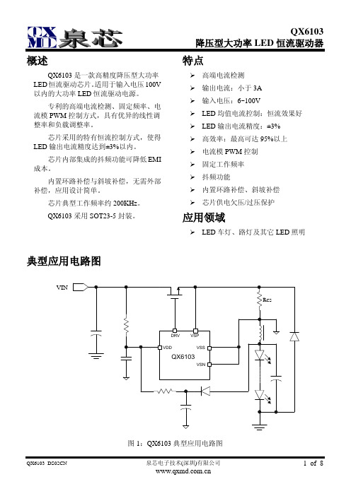
电流检测电阻 两端电压均值
VSEN
限流值
VSEN_LMT
前沿消隐时间
TLEB
OSC 工作频率
典型工作频率 抖频范围
输出驱动
FOSC ΔFOSC
上升时间
TR
下降时间
TF
QX6103 降压型大功率 LED 恒流驱动器
测试条件 最小值 典型值 最大值 单位
VDD 上升 VDD 下降
VDD =4V
5
V
4.8
芯片供电
芯片在 TOFF 期间通过辅助供电电阻 对芯片供电。应合理选择供电电阻的取值, 保证供电电流大于芯片工作电流,同时供 电电流也不宜超过 12mA,否则会超过芯 片电源引脚的箝位能力并可能导致芯片过 热。
PCB 设计
在设计 PCB 时应遵循以下指南: (1)旁路电容 VDD 的旁路电容需要紧靠芯片的 VDD 和 VSS 引脚。 (2)地线 电流采样引脚 VSN 需要用单独的走 线连接至电流采样电阻的一端。芯片地以 及其它信号地应分头接到旁路电容的地 端。
(3)功率环路 减小功率环路的面积,可减小 EMI 辐射。
QX6103_DS02CN
泉芯电子技术(深圳)有限公司
6 of 8
封装信息
SOT23-5 封装尺寸图:
QX6103 降压型大功率 LED 恒流驱动器
QX6103_DS02CN
泉芯电子技术(深圳)有限公司
LED 工作电流设定
LED 电流由接在 VSP 与 VSN 引脚之 间的电阻 RCS 设置:
I LED
=
VSEN RCS
其中,VSEN 典型值为 200mV。
电感选择
在输入电压、输出电压以及输出电流 已定的条件下,电感值决定了电感电流纹 波大小以及连续或非连续工作模式。工作 于临界模式时的电感值为:
北京海洋兴业科技股份有限公司 EMS61000-10A 阻尼振荡磁场发生器 商品说明书

EMS61000-10A 阻尼振荡磁场发生器
住宅区和商业区、工矿企业和发电厂、中压高压变电所附近产生的工频磁场及工业设施、发电厂、中高压变电所附件产生的脉冲磁场,均会对电子设备性能造成不同程度的劣化。
磁场抗扰度用于评价所处在磁场环境中的电气和电子设备的抗磁场骚扰能力,主要的依据标准是IEC61000-4-10/GB T 17626.10.
阻尼振荡磁场主要由高压变电站中的隔离刀闸切合高压母线时产生,主要适用于安装在高压变电所中的电子设备。
图示试验波形为阻尼振荡波。
839145 |
1
EMS61000-10A阻尼振荡磁场发生器是符合IEC标准IEC61000-4-10的试验仪器。
仪器用于模拟高压变电站中的隔离刀闸切合高压母线时产生的阻尼振荡磁场,为评估家用、商业和工业用途电气和电子设备的抗扰度提供一个理想、规范的依据。
技术参数:
型号EMS61000-10A阻尼振荡磁场发生器阻尼振荡磁场强度0A/m~100A/m
阻尼特性3个~6个周波内衰减至第一峰峰值的50%
振荡频率100kHz/1MHz
试验持续时间1s~99999s
脉冲极性正、负或自动交替
矩形线圈尺寸1000mm×1000mm
订货信息:
EMS61000-10A:阻尼振荡磁场发生器
标配附件:
主机、光盘、用户手册、电源线、保险丝、磁场线圈、RS232通讯线、RS232/485通讯转换器。
2
839145| ************************|。