MSP430F2013IPWR
msp430各功能模块的介绍

各个时钟信号源介绍如下:1、LFXT1CLK:低频/高频时钟源。
可以外接32768Hz的时钟芯片或频率为450KHz~8MHz的标准警惕或共振器。
2、XT2CLK:高频时钟源。
需要外接两个震荡电容器。
可以外接32768Hz的时钟芯片或频率为450KHz~8MHz的标准警惕或共振器和外部时钟输入。
较常用的晶体是8MHz的。
3、DCOCLK:内部数字可控制的RC振荡器。
MSP430单片机时钟模块提供3个时钟信号以供给片内各部分电路使用,这3个时钟信号分别是:(1)ACLK:辅助时钟信号。
ACLK是从LFXT1CLK信号由1/2/4/8分频器分频后得到的。
由BCSCTL1寄存器设置DIV A相应位来决定分频因子。
ACLK可提供给CPU外围功能模块做时钟信号使用。
(2)MCLK:主时钟信号。
MCLK是由3个时钟源所提供的。
它们分别是:LFXT1CLK、XT2CLK、和DCO时钟源信号。
MCLK主要用于MCU和相关模块做时钟。
同样可设置相关寄存器来决定分频因子及相关设置。
(3)SMCLK:子系统时钟。
SMCLK由2个时钟源信号提供,他们分别是XT2CLK 和DCO。
如果是F11或F11X1系列单片机,则由LFXT1CLK代替XT2CLK。
同样可设置相关寄存器来决定分频因子及相关的设置。
低频振荡器LFXT1:LFXT1支持超低功耗,它在低频模式下使用一个32768Hz的晶体。
不需要任何电容因为在低频模式下内部集成了电容。
低频振荡器也支持高频模式和高速晶体,但连接时每端必须加电容。
电容的大小根据所接晶体频率的高低来选择。
低频振荡器在低频和高频模式下都可以选择从XIN引脚接入一个外部输入时钟信号,但所接频率必须根据所设定的工作模式来选择,并且OSCOFF位必须复位。
高频振荡器LFXT2:LFXT2作为MSP430的第二晶体振荡器。
与低频相比,其功耗更大。
高频晶体真大气外接在XIN2和XOUT2两个引脚,并且必须外接电容。
TI(德州仪器)公司产品导购手册
TI(德州仪器)德州仪器,简称TI,全球约 30,300人,总部位于美国得克萨斯州的达拉斯,2008年营业额为185亿美元, 是全球领先的半导体公司,为现实世界的信号处理提供创新的数字信号处理(DSP)及模拟技术, 应用领域涵盖无线通讯、宽带、网络家电、数字马达控制与消费类市场。
TI(德州仪器)目录更多关于产品•MSP430系列单片机•TMS370系列单片机•TMS470系列单片机•Stellaris系列单片机•32位C2000单片机•C2000 DSP•C5000 DSP•C6000 DSP•达芬奇 DSP•A/D转换器•D/A转换器•电池管理•PWM控制器•DC/DC控制器MSP430系列单片机MSP430 系列是一个 16 位的、具有精简指令集的、超低功耗的混合型单片机,在 1996 年问世,由于它具有极低的功耗、丰富的片内外设和方便灵活的开发手段,已成为众多单片机系列中一颗耀眼的新星。
MSP430 系列单片机的迅速发展和应用范围的不断扩大,主要取决于以下的特点。
强大的处理能力 MSP430 系列单片机是一个 16 位的单片机,采用了精简指令集( RISC )结构,具有丰富的寻址方式( 7 种源操作数寻址、 4 种目的操作数寻址)、简洁的 27 条内核指令以及大量的模拟指令;大量的寄存器以及片内数据存储器都可参加多种运算;还有高效的查表处理指令;有较高的处理速度,在 8MHz 晶体驱动下指令周期为 125 ns 。
这些特点保证了可编制出高效率的源程序。
在运算速度方面, MSP430 系列单片机能在 8MHz 晶体的驱动下,实现 125ns 的指令周期。
16 位的数据宽度、 125ns 的指令周期以及多功能的硬件乘法器(能实现乘加)相配合,能实现数字信号处理的某些算法(如 FFT 等)。
MSP430 系列单片机的中断源较多,并且可以任意嵌套,使用时灵活方便。
当系统处于省电的备用状态时,用中断请求将它唤醒只用 6us 。
msp430f2013

D Ultrafast Wake-Up From Standby Mode in Less Than 1µsD 16-Bit RISC Architecture,62.5ns Instruction Cycle TimeDBasic Clock Module Configurations:--Internal Frequencies up to 16MHz With Four Calibrated Frequencies to ±1%--Internal Very Low Power LF Oscillator --32-kHz Crystal --External Digital Clock SourceD 16-Bit Timer_A With Two Capture/Compare RegistersD On-Chip Comparator for Analog Signal Compare Function or Slope A/D (MSP430x20x1only)D 10-Bit 200-ksps A/D Converter With Internal Reference,Sample-and-Hold,and Autoscan (MSP430x20x2only)D 16-Bit Sigma-Delta A/D Converter With Differential PGA Inputs and Internal Reference (MSP430x20x3only)DUniversal Serial Interface (USI)Supporting SPI and I2C(MSP430x20x2and MSP430x20x3only)InterfaceDFamily Members Include:MSP430F2001:1KB +256B Flash Memory128B RAMMSP430F2011:2KB +256B Flash Memory128B RAMMSP430F2002:1KB +256B Flash Memory128B RAMMSP430F2012:2KB +256B Flash Memory128B RAMMSP430F2003:1KB +256B Flash Memory128B RAMMSP430F2013:2KB +256B Flash Memory128B RAMD Available in a 14-Pin Plastic Small-Outline Thin Package (TSSOP),14-Pin Plastic Dual Inline Package (PDIP),and 16-Pin QFNDFor Complete Module Descriptions,See the MSP430x2xx Family User’s GuidedescriptionThe Texas Instruments MSP430family of ultralow-power microcontrollers consist of several devices featuring different sets of peripherals targeted for various applications.The architecture,combined with five low-power modes is optimized to achieve extended battery life in portable measurement applications.The device features a powerful 16-bit RISC CPU,16-bit registers,and constant generators that contribute to maximum code efficiency.The digitally controlled oscillator (DCO)allows wake-up from low-power modes to active mode in less than 1µs.The MSP430x20xx series is an ultralow-power mixed signal microcontroller with a built-in 16-bit timer,and ten I/O pins.In addition the MSP430x20x1has a versatile analog comparator.The MSP430x20x2and MSP430x20x3have built-in communication capability using synchronous protocols (SPI or I2C),and a 10-bit A/D converter (MSP430x20x2)or a 16-bit sigma-delta A/D converter (MSP430x20x3).Typical applications include sensor systems that capture analog signals,convert them to digital values,and then process the data for display or for transmission to a host system.Stand alone RF sensor front end is another area of application.Please be aware that an important notice concerning availability,standard warranty,and use in critical applications of Texas Instruments semiconductor products and disclaimers thereto appears at the end of this data sheet.PRODUCTION DATA information is current as of publication date.Products conform to specifications per the terms of Texas Instruments standard warranty.Production processing does not necessarily include testing of all parameters.AVAILABLE OPTIONSPACKAGED DEVICEST APLASTIC 14-PIN TSSOP(PW)PLASTIC 14-PIN DIP(N)PLASTIC 16-PIN QFN (RSA)--40°C to 85°CMSP430F2001IPW MSP430F2011IPW MSP430F2002IPW MSP430F2012IPW MSP430F2003IPW MSP430F2013IPW MSP430F2001IN MSP430F2011IN MSP430F2002IN MSP430F2012IN MSP430F2003INMSP430F2013IN MSP430F2001IRSA MSP430F2011IRSA MSP430F2002IRSA MSP430F2012IRSA MSP430F2003IRSA MSP430F2013IRSA --40°C to 105°CMSP430F2001TPW MSP430F2011TPW MSP430F2002TPW MSP430F2012TPW MSP430F2003TPW MSP430F2013TPWMSP430F2001TN MSP430F2011TN MSP430F2002TN MSP430F2012TN MSP430F2003TN MSP430F2013TNMSP430F2001TRSA MSP430F2011TRSA MSP430F2002TRSA MSP430F2012TRSA MSP430F2003TRSA MSP430F2013TRSAdevice pinout,MSP430x20x1V CCP1.5/TA0/CA5/TMSP1.3/CAOUT/CA3P1.2/TA1/CA2P1.1/TA0/CA1P1.0/TACLK/ACLK/CA0P1.4/SMCLK/CA4/TCKPW or N PACKAGE(TOP VIEW)TEST/SBWTCK XOUT/P2.7XIN/P2.6/TA1RST/NMI/SBWTDIOP 1.7/C A O U T /C A 7/T D O /T D IP 1.6/T A 1/C A 6/T D I /T C L KP 1.4/S M C L K /C A 4/T C KP 1.5/T A 0/C A 5/T M SNOTE:See port schematics section for detailed I/O information.device pinout,MSP430x20x2V CCP1.5/TA0/A5/SCLK/TMSP1.3/ADC10CLK/A3/VREF--/VeREF--P1.2/TA1/A2P1.1/TA0/A1P1.0/TACLK/ACLK/A0P1.4/SMCLK/A4/VREF+/VeREF+/TCKPW or N PACKAGE(TOP VIEW)TEST/SBWTCK XOUT/P2.7XIN/P2.6/TA1RST/NMI/SBWTDIOP 1.7/A 7/S D I /S D A /T D O /T D IP 1.6/T A 1/A 6/S D O /S C L /T D I /T C L KP 1.4/S M C L K /A 4/V R E F +/V e R E F +/T C KP 1.5/T A 0/A 5/S C L K /T M SNOTE:See port schematics section for detailed I/O information.device pinout,MSP430x20x3V CCP1.5/TA0/A2--/SCLK/TMSP1.3/VREF/A1--P1.2/TA1/A1+/A4--P1.1/TA0/A0--/A4+P1.0/TACLK/ACLK/A0+P1.4/SMCLK/A2+/TCK PW or N PACKAGE(TOP VIEW)TEST/SBWTCK XOUT/P2.7XIN/P2.6/TA1RST/NMI/SBWTDIOP 1.7/A 3--/S D I /S D A /T D O /T D IP 1.6/T A 1/A 3+/S D O /S C L /T D I /T C L KP 1.4/S M C L K /A 2+/T C KP 1.5/T A 0/A 2--/S C L K /T M SNOTE:See port schematics section for detailed I/O information.functional block diagram,MSP430x20x1RST/NMIVCCVSSP1.x &JTAGP2.x &NOTE:See port schematics section for detailed I/O information.functional block diagram,MSP430x20x2RST/NMIVCCVSSP1.x &JTAGP2.x &NOTE:See port schematics section for detailed I/O information.functional block diagram,MSP430x20x3RST/NMIVCCVSSP1.x &JTAGP2.x &NOTE:See port schematics section for detailed I/O information.Terminal Functions,MSP430x20x1 TERMINALPW or N RSA NAMENO.NO.I/ODESCRIPTIONP1.0/TACLK/ACLK/CA021I/O General-purpose digital I/O pinTimer_A,clock signal TACLK inputACLK signal ouputComparator_A+,CA0inputP1.1/TA0/CA132I/O General-purpose digital I/O pinTimer_A,capture:CCI0A input,compare:Out0outputComparator_A+,CA1inputP1.2/TA1/CA243I/O General-purpose digital I/O pinTimer_A,capture:CCI1A input,compare:Out1outputComparator_A+,CA2inputP1.3/CAOUT/CA354I/O General-purpose digital I/O pinComparator_A+,output/CA3inputP1.4/SMCLK/C4/TCK65I/O General-purpose digital I/O pinSMCLK signal outputComparator_A+,CA4inputJTAG test clock,input terminal for device programming and testP1.5/TA0/CA5/TMS76I/O General-purpose digital I/O pinTimer_A,compare:Out0outputComparator_A+,CA5inputJTAG test mode select,input terminal for device programming and test P1.6/TA1/CA6/TDI/TCLK87I/O General-purpose digital I/O pinTimer_A,compare:Out1outputComparator_A+,CA6inputJTAG test data input or test clock input during programming and testP1.7/CAOUT/CA7/TDO/TDI†98I/O General-purpose digital I/O pinComparator_A+,output/CA7inputJTAG test data output terminal or test data input during programming andtestXIN/P2.6/TA11312I/O Input terminal of crystal oscillatorGeneral-purpose digital I/O pinTimer_A,compare:Out1outputXOUT/P2.71211I/O Output terminal of crystal oscillatorGeneral-purpose digital I/O pinRST/NMI/SBWTDIO109I Reset or nonmaskable interrupt inputSpy-Bi-Wire test data input/output during programming and testTEST/SBWTCK1110I Selects test mode for JTAG pins on Port1.The device protection fuse isconnected to TEST.Spy-Bi-Wire test clock input during programming and testV CC116Supply voltageV SS1414Ground referenceNC NA13,15Not connectedQFN Pad NA PackagePadNA QFN package pad connection to V SS recommended.†TDO or TDI is selected via JTAG instruction.NOTE:If XOUT/P2.7is used as an input,excess current will flow until P2SEL.7is cleared.This is due to the oscillator output driver connection to this pad after reset.Terminal Functions,MSP430x20x2 TERMINALPW,or N RSA NAMENO.NO.I/ODESCRIPTIONP1.0/TACLK/ACLK/A021I/O General-purpose digital I/O pinTimer_A,clock signal TACLK inputACLK signal ouputADC10analog input A0P1.1/TA0/A132I/O General-purpose digital I/O pinTimer_A,capture:CCI0A input,compare:Out0outputADC10analog input A1P1.2/TA1/A243I/O General-purpose digital I/O pinTimer_A,capture:CCI1A input,compare:Out1outputADC10analog input A2P1.3/ADC10CLK/ A3/VREF--/VeREF--54I/O General-purpose digital I/O pinADC10conversion clock outputADC10analog input A3Input for negative external reference voltage/negative internal referencevoltage outputP1.4/SMCLK/A4/VREF+/VeREF+/ TCK 65I/O General-purpose digital I/O pinSMCLK signal outputADC10analog input A4Input for positive external reference voltage/positive internal referencevoltage outputJTAG test clock,input terminal for device programming and testP1.5/TA0/A5/SCLK/TMS76I/O General-purpose digital I/O pinTimer_A,compare:Out0outputADC10analog input A5USI:external clock input in SPI or I2C mode;clock output in SPI modeJTAG test mode select,input terminal for device programming and test P1.6/TA1/A6/SDO/SCL/TDI/TCLK87I/O General-purpose digital I/O pinTimer_A,capture:CCI1B input,compare:Out1outputADC10analog input A6USI:Data output in SPI mode;I2C clock in I2C modeJTAG test data input or test clock input during programming and testP1.7/A7/SDI/SDA/TDO/TDI†98I/O General-purpose digital I/O pinADC10analog input A7USI:Data input in SPI mode;I2C data in I2C modeJTAG test data output terminal or test data input during programming andtestXIN/P2.6/TA11312I/O Input terminal of crystal oscillatorGeneral-purpose digital I/O pinTimer_A,compare:Out1outputXOUT/P2.71211I/O Output terminal of crystal oscillatorGeneral-purpose digital I/O pinRST/NMI/SBWTDIO109I Reset or nonmaskable interrupt inputSpy-Bi-Wire test data input/output during programming and testTEST/SBWTCK1110I Selects test mode for JTAG pins on Port1.The device protection fuse isconnected to TEST.Spy-Bi-Wire test clock input during programming and testV CC1NA Supply voltageV SS14NA Ground reference†TDO or TDI is selected via JTAG instruction.NOTE:If XOUT/P2.7is used as an input,excess current will flow until P2SEL.7is cleared.This is due to the oscillator output driver connection to this pad after reset.Terminal Functions,MSP430x20x2(Continued) TERMINALPW,or N RSA NAMENO.NO.I/ODESCRIPTIONDV CC NA16Digital supply voltageAV CC NA15Analog supply voltageDV SS NA14Digital ground referenceAV SS NA13Analog ground referenceQFN Pad NA PackagePadNA QFN package pad connection to V SS recommended.Terminal Functions,MSP430x20x3TERMINALPW,or N RSA NAMENO.NO.I/ODESCRIPTIONP1.0/TACLK/ACLK/A0+21I/O General-purpose digital I/O pinTimer_A,clock signal TACLK inputACLK signal ouputSD16_A positive analog input A0P1.1/TA0/A0--/A4+32I/O General-purpose digital I/O pinTimer_A,capture:CCI0A input,compare:Out0outputSD16_A negative analog input A0SD16_A positive analog input A4P1.2/TA1/A1+/A4--43I/O General-purpose digital I/O pinTimer_A,capture:CCI1A input,compare:Out1outputSD16_A positive analog input A1SD16_A negative analog input A4P1.3/VREF/A1--54I/O General-purpose digital I/O pinInput for an external reference voltage/internal reference voltage output(can be used as mid-voltage)SD16_A negative analog input A1P1.4/SMCLK/A2+/TCK65I/O General-purpose digital I/O pinSMCLK signal outputSD16_A positive analog input A2JTAG test clock,input terminal for device programming and testP1.5/TA0/A2--/SCLK/TMS76I/O General-purpose digital I/O pinTimer_A,compare:Out0outputSD16_A negative analog input A2USI:external clock input in SPI or I2C mode;clock output in SPI modeJTAG test mode select,input terminal for device programming and test P1.6/TA1/A3+/SDO/SCL/TDI/TCLK87I/O General-purpose digital I/O pinTimer_A,capture:CCI1B input,compare:Out1outputSD16_A positive analog input A3USI:Data output in SPI mode;I2C clock in I2C modeJTAG test data input or test clock input during programming and test P1.7/A3--/SDI/SDA/TDO/TDI†98I/O General-purpose digital I/O pinSD16_A negative analog input A3USI:Data input in SPI mode;I2C data in I2C modeJTAG test data output terminal or test data input during programming andtest†TDO or TDI is selected via JTAG instruction.Terminal Functions,MSP430x20x3(Continued) TERMINALPW,or N RSA NAMENO.NO.I/ODESCRIPTIONXIN/P2.6/TA11312I/O Input terminal of crystal oscillatorGeneral-purpose digital I/O pinTimer_A,compare:Out1outputXOUT/P2.71211I/O Output terminal of crystal oscillatorGeneral-purpose digital I/O pinRST/NMI/SBWTDIO109I Reset or nonmaskable interrupt inputSpy-Bi-Wire test data input/output during programming and testTEST/SBWTCK1110I Selects test mode for JTAG pins on Port1.The device protection fuse isconnected to TEST.Spy-Bi-Wire test clock input during programming and testV CC1NA Supply voltageV SS14NA Ground referenceDV CC NA16Digital supply voltageAV CC NA15Analog supply voltageDV SS NA14Digital ground referenceAV SS NA13Analog ground referenceQFN Pad NA PackagePadNA QFN package pad connection to V SS recommended.NOTE:If XOUT/P2.7is used as an input,excess current will flow until P2SEL.7is cleared.This is due to the oscillator output driver connection to this pad after reset.General-Purpose Register Program Counter Stack Pointer Status Register Constant Generator General-Purpose Register General-Purpose Register General-Purpose Register PC/R0SP/R1SR/CG1/R2CG2/R3R4R5R12R13General-Purpose Register General-Purpose Register R6R7General-Purpose Register General-Purpose Register R8R9General-Purpose Register General-Purpose Register R10R11General-Purpose Register General-Purpose RegisterR14R15short-form descriptionCPUThe MSP430CPU has a 16-bit RISC architecture that is highly transparent to the application.All operations,other than program-flow instructions,are performed as register operations in conjunction with seven addressing modes for source operand and four addressing modes for destination operand.The CPU is integrated with 16registers that provide reduced instruction execution time.The register-to-register operation execution time is one cycle of the CPU clock.Four of the registers,R0to R3,are dedicated as program counter,stack pointer,status register,and constant generator respectively.The remaining registers are general-purpose registers.Peripherals are connected to the CPU using data,address,and control buses,and can be handled with all instructions.instruction setThe instruction set consists of 51instructions with three formats and seven address modes.Each instruction can operate on word and byte data.Table 1shows examples of the three types of instruction formats;the address modes are listed in Table 2.Table 1.Instruction Word FormatsDual operands,source-destination e.g.,ADD R4,R5R4+R5------>R5Single operands,destination only e.g.,CALL R8PC ---->(TOS),R8---->PC Relative jump,un/conditionale.g.,JNEJump-on-equal bit =0Table 2.Address Mode DescriptionsADDRESS MODES D SYNTAX EXAMPLE OPERATION Register F F MOV Rs,Rd MOV R10,R11R10---->R11IndexedF F MOV X(Rn),Y(Rm)MOV 2(R5),6(R6)M(2+R5)---->M(6+R6)Symbolic (PC relative)F F MOV EDE,TONI M(EDE)---->M(TONI)Absolute F F MOV &MEM,&TCDAT M(MEM)---->M(TCDAT)Indirect F MOV @Rn,Y(Rm)MOV @R10,Tab(R6)M(R10)---->M(Tab+R6)Indirect autoincrement F MOV @Rn+,Rm MOV @R10+,R11M(R10)---->R11R10+2---->R10ImmediateFMOV #X,TONIMOV #45,TONI #45---->M(TONI)NOTE:S =sourceD =destinationoperating modesThe MSP430has one active mode and five software-selectable low-power modes of operation.An interrupt event can wake up the device from any of the five low-power modes,service the request,and restore back to the low-power mode on return from the interrupt program.The following six operating modes can be configured by software:D Active mode AM;--All clocks are activeD Low-power mode0(LPM0);--CPU is disabledACLK and SMCLK remain active.MCLK is disabledD Low-power mode1(LPM1);--CPU is disabledACLK and SMCLK remain active.MCLK is disabledDCO’s dc-generator is disabled if DCO not used in active modeD Low-power mode2(LPM2);--CPU is disabledMCLK and SMCLK are disabledDCO’s dc-generator remains enabledACLK remains activeD Low-power mode3(LPM3);--CPU is disabledMCLK and SMCLK are disabledDCO’s dc-generator is disabledACLK remains activeD Low-power mode4(LPM4);--CPU is disabledACLK is disabledMCLK and SMCLK are disabledDCO’s dc-generator is disabledCrystal oscillator is stoppedinterrupt vector addressesThe interrupt vectors and the power-up starting address are located in the address range of0FFFFh--0FFC0h.The vector contains the16-bit address of the appropriate interrupt handler instruction sequence.If the reset vector(located at address0FFFEh)contains0FFFFh(e.g.,flash is not programmed)the CPU will go into LPM4immediately after power-up.INTERRUPT SOURCE INTERRUPT FLAG SYSTEM INTERRUPT WORD ADDRESS PRIORITYPower-upExternal resetWatchdog Timer+Flash key violationPC out-of-range(see Note1)PORIFGRSTIFGWDTIFGKEYV(see Note2)Reset0FFFEh31,highestNMIOscillator faultFlash memory access violationNMIIFGOFIFGACCVIFG(see Notes2and4)(non)-maskable,(non)-maskable,(non)-maskable0FFFCh300FFFAh290FFF8h28Comparator_A+(MSP430x20x1only)CAIFG(see Note3)maskable0FFF6h27 Watchdog Timer+WDTIFG maskable0FFF4h26 Timer_A2TACCR0CCIFG(see Note3)maskable0FFF2h25Timer_A2TACCR1CCIFG.TAIFG(see Notes2and3)maskable0FFF0h240FFEEh230FFECh22ADC10(MSP430x20x2only)ADC10IFG(see Note3)maskableSD16_A(MSP430x20x3only)SD16CCTL0SD16OVIFG,SD16CCTL0SD16IFG(see Notes2and3)maskable0FFEAh21USI(MSP430x20x2,MSP430x20x3only)USIIFG,USISTTIFG(see Notes2and3)maskable0FFE8h20I/O Port P2 (two flags)P2IFG.6to P2IFG.7(see Notes2and3)maskable0FFE6h19I/O Port P1 (eight flags)P1IFG.0to P1IFG.7(see Notes2and3)maskable0FFE4h180FFE2h170FFE0h16(see Note5)0FFDEh...0FFC0h15...0,lowest NOTES: 1.A reset is generated if the CPU tries to fetch instructions from within the module register memory address range(0h--01FFh)or from within unused address ranges.2.Multiple source flags3.Interrupt flags are located in the module4.(non)-maskable:the individual interrupt-enable bit can disable an interrupt event,but the general interrupt enable cannot.5.The interrupt vectors at addresses0FFDEh to0FFC0h are not used in this device and can be used for regular program code ifnecessary.special function registersMost interrupt and module enable bits are collected into the lowest address space.Special function register bits not allocated to a functional purpose are not physically present in the device.Simple software access is provided with this arrangement.interrupt enable 1and2rw-0rw-0rw-0Address 0hrw-0WDTIE:Watchdog Timer interrupt enable.Inactive if watchdog mode is selected.Active if Watchdog Timer is configured in interval timer mode.OFIE:Oscillator fault enableNMIIE:(Non)maskable interrupt enableACCVIE:Flash access violation interruptenableAddress 01hinterrupt flag register 1and2rw-0rw-1rw-(0)Address 02hrw-(0)rw-(1)WDTIFG:Set on Watchdog Timer overflow (in watchdog mode)or security key violation.Reset on V CC power-up or a reset condition at RST/NMI pin in reset mode.OFIFG:Flag set on oscillator faultRSTIFG:External reset interrupt flag.Set on a reset condition at RST/NMI pin in reset mode.Reset on V CC power-upPORIFG:Power-On Reset interrupt flag.Set on V CC power-up.NMIIFG:Set viaRST/NMI-pinAddress03hLegendrw:rw-0,1:Bit can be read and written.Bit can be read and written.It is Reset or Set by PUC.Bit can be read and written.It is Reset or Set by POR.rw-(0,1):SFR bit is not present in devicememory organizationMSP430F200x MSP430F201xMemoryMain:interrupt vector Main:code memorySizeFlashFlash1KB Flash0FFFFh--0FFC0h0FFFFh--0FC00h2KB Flash0FFFFh--0FFC0h0FFFFh--0F800hInformation memory SizeFlash256Byte010FFh--01000h256Byte010FFh--01000hRAM Size128Byte027Fh--0200h128Byte 027Fh--0200hPeripherals16-bit8-bit8-bit SFR 01FFh--0100h0FFh--010h0Fh--00h01FFh--0100h0FFh--010h0Fh--00hflash memoryThe flash memory can be programmed via the Spy-Bi-Wire/JTAG port,or in-system by the CPU.The CPU can perform single-byte and single-word writes to the flash memory.Features of the flash memory include:D Flash memory has n segments of main memory and four segments of information memory(A to D)of64bytes each.Each segment in main memory is512bytes in size.D Segments0to n may be erased in one step,or each segment may be individually erased.D Segments A to D can be erased individually,or as a group with segments0--n.Segments A to D are also called information memory.D Segment A contains calibration data.After reset segment A is protected against programming and erasing.It can be unlocked but care should be taken not to erase this segment if the device-specific calibration data is required.peripheralsPeripherals are connected to the CPU through data,address,and control busses and can be handled using all instructions.For complete module descriptions,refer to the MSP430x2xx Family User’s Guide. oscillator and system clockThe clock system is supported by the basic clock module that includes support for a32768-Hz watch crystal oscillator,an internal very-low-power low-frequency oscillator and an internal digitally-controlled oscillator (DCO).The basic clock module is designed to meet the requirements of both low system cost and low power consumption.The internal DCO provides a fast turn-on clock source and stabilizes in less than1µs.The basic clock module provides the following clock signals:D Auxiliary clock(ACLK),sourced either from a32768-Hz watch crystal or the internal LF oscillator.D Main clock(MCLK),the system clock used by the CPU.D Sub-Main clock(SMCLK),the sub-system clock used by the peripheral modules.DCO Calibration Data(provided from factory in flash info memory segment A)DCO Frequency Calibration Register Size Address1MHz CALBC1_1MHZ byte010FFhCALDCO_1MHZ byte010FEh8MHz CALBC1_8MHZ byte010FDhCALDCO_8MHZ byte010FCh12MHz CALBC1_12MHZ byte010FBhCALDCO_12MHZ byte010FAh16MHz CALBC1_16MHZ byte010F9hCALDCO_16MHZ byte010F8hbrownoutThe brownout circuit is implemented to provide the proper internal reset signal to the device during power on and power off.digital I/OThere is one8-bit I/O port implemented—port P1—and two bits of I/O port P2:D All individual I/O bits are independently programmable.D Any combination of input,output,and interrupt condition is possible.D Edge-selectable interrupt input capability for all the eight bits of port P1and the two bits of port P2.D Read/write access to port-control registers is supported by all instructions.D Each I/O has an individually programmable pull-up/pull-down resistor.WDT+watchdog timerThe primary function of the watchdog timer(WDT+)module is to perform a controlled system restart after a software problem occurs.If the selected time interval expires,a system reset is generated.If the watchdog function is not needed in an application,the module can be disabled or configured as an interval timer and can generate interrupts at selected time intervals.timer_A2Timer_A2is a 16-bit timer/counter with two capture/compare registers.Timer_A2can support multiple capture/compares,PWM outputs,and interval timing.Timer_A2also has extensive interrupt capabilities.Interrupts may be generated from the counter on overflow conditions and from each of the capture/compare registers.Timer_A2Signal Connections (MSP43020x1only)Input Pin Number Device Input SignalModule Input NameModule BlockModule Output SignalOutput Pin Number PW,N RSA PW,NRSA2-P1.01-P1.0TACLK TACLK ACLK ACLK SMCLKSMCLK TimerNA2-P1.01-P1.0TACLK INCLK 3-P1.12-P1.1TA0CCI0A 3-P1.12-P1.1ACLK (internal)CCI0B 7-P1.56-P1.5V SS GND CCR0TA0V CCV CC 4-P1.23-P1.2TA1CCI1A 4-P1.23-P1.2CAOUT (internal)CCI1B 8-P1.67-P1.6V SS GND CCR1TA113-P2.612-P2.6V CCV CCTimer_A2Signal Connections (MSP430F20x2,MSP430F20x3)Input Pin Number Device Input SignalModule Input NameModule BlockModule Output SignalOutput Pin Number PW,N RSA PW,NRSA2-P1.01-P1.0TACLK TACLK ACLK ACLK SMCLKSMCLK TimerNA2-P1.01-P1.0TACLK INCLK 3-P1.12-P1.1TA0CCI0A 3-P1.12-P1.17-P1.56-P1.5ACLK (internal)CCI0B 7-P1.56-P1.5V SS GND CCR0TA0V CCV CC 4-P1.23-P1.2TA1CCI1A 4-P1.23-P1.28-P1.67-P1.6TA1CCI1B 8-P1.67-P1.6V SS GND CCR1TA113-P2.612-P2.6V CCV CCcomparator_A+(MSP430x20x1only)The primary function of the comparator_A+module is to support precision slope analog-to-digital conversions,battery-voltage supervision,and monitoring of external analog signals.USI(MSP430x20x2and MSP430x20x3only)The universal serial interface(USI)module is used for serial data communication and provides the basic hardware for synchronous communication protocols like SPI and I2C.ADC10(MSP430x20x2only)The ADC10module supports fast,10-bit analog-to-digital conversions.The module implements a10-bit SAR core,sample select control,reference generator and data transfer controller,or DTC,for automatic conversion result handling,allowing ADC samples to be converted and stored without any CPU intervention.SD16_A(MSP430x20x3only)The SD16_A module supports16-bit analog-to-digital conversions.The module implements a16-bit sigma-delta core and reference generator.In addition to external analog inputs,internal V CC sense and temperature sensors are also available.peripheral file mapPERIPHERALS WITH WORD ACCESSADC10(MSP430x20x2only)ADC control0ADC control1ADC memory ADC10CTL0ADC10CTL1ADC10MEM01B0h01B2h01B4hSD16_A(MSP430x20x3only)General ControlChannel0ControlInterrupt vector word registerChannel0conversion memory SD16CTLSD16CCTL0SD16IVSD16MEM00100h0102h0110h0112hTimer_A Capture/compare registerCapture/compare registerTimer_A registerCapture/compare controlCapture/compare controlTimer_A controlTimer_A interrupt vector TACCR1TACCR0TARTACCTL1TACCTL0TACTLTAIV0174h0172h0170h0164h0162h0160h012EhFlash Memory Flash control3Flash control2Flash control1FCTL3FCTL2FCTL1012Ch012Ah0128hWatchdog Timer+Watchdog/timer control WDTCTL0120hPERIPHERALS WITH BYTE ACCESSADC10(MSP430x20x2only)Analog enable ADC10AE04AhSD16_A(MSP430x20x3only)Channel0Input ControlAnalog Enable SD16INCTL0SD16AE0B0h0B7hUSI(MSP430x20x2and MSP430x20x3only)USI control0USI control1USI clock controlUSI bit counterUSI shift registerUSICTL0USICTL1USICKCTLUSICNTUSISR078h079h07Ah07Bh07ChComparator_A+ (MSP430x20x1only)Comparator_A+port disableComparator_A+control2Comparator_A+control1CAPDCACTL2CACTL105Bh05Ah059hBasic Clock System+Basic clock system control3Basic clock system control2Basic clock system control1DCO clock frequency control BCSCTL3 BCSCTL2 BCSCTL1 DCOCTL053h058h057h056hPort P2Port P2resistor enablePort P2selectionPort P2interrupt enablePort P2interrupt edge selectPort P2interrupt flagPort P2directionPort P2outputPort P2input P2RENP2SELP2IEP2IESP2IFGP2DIRP2OUTP2IN02Fh02Eh02Dh02Ch02Bh02Ah029h028hPort P1Port P1resistor enablePort P1selectionPort P1interrupt enablePort P1interrupt edge selectPort P1interrupt flagPort P1directionPort P1outputPort P1input P1RENP1SELP1IEP1IESP1IFGP1DIRP1OUTP1IN027h026h025h024h023h022h021h020hSpecial Function SFR interrupt flag2SFR interrupt flag1SFR interrupt enable2SFR interrupt enable1IFG2IFG1IE2IE1003h002h001h000h。
MSP430自制LED怀表

MSP430自制LED怀表(本文转自我爱方案网论坛)1、必备的条件首先是具有2线制调试接口的MSP430系列单片机的仿真器,我自己使用的型号是MSP-FET430UIF,是从利尔达公司买的。
同时你还需要有对应的IDE环境,以及一定的调试能力。
其次,应该有一把尖头镊子。
因为板子上的0603封装的LED排列相对紧密,所以一把好的镊子能很好地解决焊接时夹放元件的问题。
再次,应该有一柄具有尖头的烙铁,理由同上。
最后,热风台。
因为板子上有QFN封装的芯片——加速度传感器。
我是利用热风台焊接的,以前有介绍说用烙铁焊的,但是我一直是用热风台来做这个活的此外,一些比较细的热缩管、一小段高温导线以及一块鼠标板作为焊接时的工作面(用鼠标板反面做焊接面,板子不会滑动,而且不晃眼)……当然,你最好还有焊锡、助焊剂、热熔胶、导热硅胶、电脑、万用表、示波器等等2 焊接清点元件打开你买到的元件盒后,应仔细清点你元件盒里是不是有以下清单里的全部元件。
我觉得你不会把各个元件弄混的。
里面有一个地方要说明,考虑到大家焊接的损失,红、黄、绿三色的LED在清单上是各55个,但实际上我在分装时是按照60只分装的。
MSP430F4152 1PCSMMA7660 1PCSTMP102 1PCS蜂鸣器 1PCS32k晶体 1PCS全彩LED 12PCS蓝色LED 13PCS红色LED 55PCS黄色LED 55PCS绿色LED 55 PCS大、小PCB 各1 PCS怀表表壳 1 PCS怀表表拴 1 PCS电池 1PCS100欧 12 PCS4.7K 2 PCS10K 4 PCS104电容 2 PCS拨码开关 1PCS首先注意元件的焊接位置和方向,跟原理图稍微不太对应:大板的内外圈LED方向和原理图是反的,小板的星期一的LED和底下数码其中一个是反的。
即网络标号为CRZ6和CRZ4的两个LED。
以这个几个图为准进行焊接。
注意芯片的方向,芯片的型号就不列了,这个焊不错的。
eZ430-F2013开发工具指南

eZ430-F2013开发工具用户指南1. eZ430-F2013 套件内容• 一个 eZ430-F2013。
硬件位于可开启的塑料盒内,以便将 MSP-EZ430D 目标板与 MSP-EZ430U 调试接口分离开来;• 一张 MSP430 开发工具 CD 光盘,内容包含与 eZ430-F2013 相关的多个文档,如:– MSP430x2xx 系列用户指南,SLAU144– MSP-FET430 FLASH 仿真工具用户指南,SLAU138– MSP-FET430 FLASH 仿真工具用户指南勘误表,SLAZ027– eZ430-F2013 用户指南(本文档)– IAR Embedded Workbench Kickstart 版– Code Composer Studio MCU 版2. eZ430-F2013 概览eZ430-F2013 是一款完整的 MSP430 开发工具,其在小巧的便携式 USB 棒状盒内提供了评估 MSP430F2013 以及完成整个项目所需的全部软硬件。
eZ430-F2013 集成了 IAR Embedded Workbench 或 Code Composer Studio 集成开发环境 (IDE),通过选择设计一个独立的系统,或选择分离可移动的目标板并整合到现有设计中来提供完全仿真。
USB 端口可为超低功耗 MSP430 提供所需的工作电源,因而无需使用外接电源。
MSP430F2013 上的所有 14 个引脚都可在 MSP-EZ430D 目标板上进行访问,可轻松实现调试并与外设接口相连。
此外,还可将其中的一个数字 I/O 引脚连接至可提供视觉反馈的 LED 。
MSP430F2013 拥有出色的 16 MIPS 性能,并高度集成了 16 位 Δ-Σ 模数转换器、16 位定时器、看门狗定时器、掉电检测器、支持 SPI 和 I 2C 的 USI 模块,以及待机电流仅 0.5 微安的 5 种低功耗模式。
MSP430单片机入门例程
MSP430单片机入门例程MSP430单片机是一款低功耗、高性能的16位单片机,广泛应用于各种嵌入式系统。
下面是一个简单的MSP430单片机入门例程,可以让大家初步了解MSP430单片机的基本使用方法。
所需材料:1、MSP430单片机开发板2、MSP430单片机编译器3、MSP430单片机调试器4、电脑和相关软件步骤:1、安装MSP430单片机编译器首先需要安装MSP430单片机的编译器,该编译器可以将C语言代码编译成MSP430单片机可以执行的机器码。
在安装编译器时,需要选择与您的单片机型号匹配的编译器。
2、编写程序下面是一个简单的MSP430单片机程序,可以让LED灯闪烁:c本文include <msp430.h>int main(void)本文P1DIR |= 0x01; //设置P1.0为输出while(1){P1OUT ^= 0x01; //反转P1.0的状态,LED闪烁__delay_cycles(); //延时一段时间,控制闪烁频率}本文上述程序中,首先定义了P1DIR寄存器,将P1.0设置为输出。
然后进入一个无限循环,在循环中反转P1.0的状态,使LED闪烁。
使用__delay_cycles()函数实现延时,控制LED闪烁频率。
3、编译程序使用MSP430单片机编译器将程序编译成机器码,生成可执行文件。
在编译时,需要注意选择正确的编译器选项和单片机型号。
4、调试程序使用MSP430单片机调试器将可执行文件下载到单片机中,并使用调试器进行调试。
在调试时,可以观察单片机的输出口状态和LED灯的闪烁情况,确保程序正常运行。
随着嵌入式系统的发展,MSP430单片机作为一种低功耗、高性能的微控制器,在各种应用领域中得到了广泛的应用。
为了更好地理解和应用MSP430单片机,我在学习过程中积累了一些经验,现在分享给大家。
MSP430单片机是一种超低功耗的微控制器,由德州仪器(Texas Instruments)推出。
MSP430单片机基础实验手册
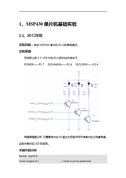
1、MSP430单片机基础实验1.1、IO口实验实验目的:学会MSP430单片机IO口的常规操作。
实验原理开发板上的3个LED灯和IO口的对应关系如下:POWER——P1.7 ISO14443A——P1.6 ISO15693——P1.4根据原理图分析,只需要将对应IO输出为低电平即可使其对应三极管导通,达到点亮对应LED的目的。
关键代码分析#include <msp430.h>volatile unsigned int i; // volatile to prevent optimizationint main(void){WDTCTL = WDTPW + WDTHOLD; // Stop watchdog timerP1DIR |= 0x80; // Set P1.7 to output directionfor (;;){P1OUT ^= 0x80; // Toggle P1.7 using exclusive-ORi = 50000; // Delaydo (i--);while (i != 0);}}对应工程详见:\感知RF2实验光盘2013\RFID技术实验\1-MSP430单片机基础实验\io实验结果POWER对应的LED灯闪烁。
作业1、对其他连个灯进行对应操作;2、流水灯显示编程控制。
1.2、定时器实验实验目的:学会MSP430单片机定时器常规配置及中断操作。
实验原理采用定时器TA溢出中断对LED灯进行取反操作。
关键代码分析#include <msp430.h>int main(void){WDTCTL = WDTPW + WDTHOLD; // Stop WDTP1DIR |= 0x80; // P1.0 outputTACCTL0 = CCIE; // TACCR0 interrupt enabledTACCR0 = 50000;TACTL = TASSEL_2 + MC_2; // SMCLK, contmode__bis_SR_register(LPM0_bits + GIE); // Enter LPM0 w/ interrupt}// Timer A0 interrupt service routine#pragma vector=TIMERA0_VECTOR__interrupt void Timer_A (void){P1OUT ^= 0x80; // Toggle P1.7TACCR0 += 50000; // Add Offset to TACCR0}对应工程详见\感知RF2实验光盘2013\RFID技术实验\1-MSP430单片机基础实验\timer实验结果LED灯快速闪烁,改变TACCR0值,闪烁时间间隔改变。
MSP430UIF使用说明
MSP430-UIF仿真器使用说明一. 功能描述0、USB接口的JTAG仿真器。
USB口取电,不需要外接电源,并能给目标板或用户板提供3.3V(300mA)电源;1、对MSP430 FLASH全系列单片机进行编程和在线仿真;2、完全兼容德州仪器原厂MSP-FET430UIF开发工具;3、可在线升级,烧熔丝加密。
4、采用德州仪器标准的2×7 PIN(IDC-14)标准连接器;5、支持IAR430、AQ430、HI-TECH、GCC以及TI一些第三方编译器集成开发环境下的实时仿真、调试、单步执行、断点设置、存储器内容查看修改等;6、支持程序烧写读取和熔丝烧断功能;7、支持JTAG、SBW(2 Wire JTAG)接口;8、支持固件升级功能。
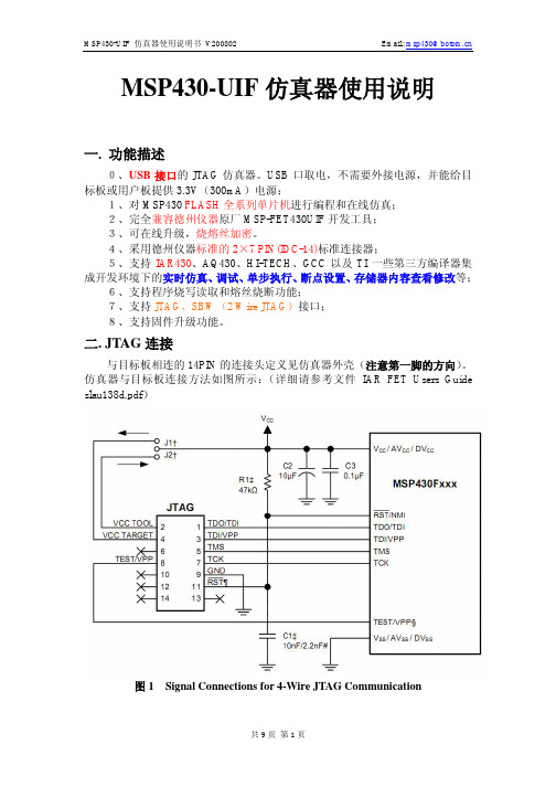
二. JTAG连接与目标板相连的14PIN的连接头定义见仿真器外壳(注意第一脚的方向)。
仿真器与目标板连接方法如图所示:(详细请参考文件IAR FET Users Guide slau138d.pdf)图1 Signal Connections for 4-Wire JTAG Communication图2 Signal Connections for 2-Wire JTAG Communication (Spy-Bi-Wire) 三. 硬件安装1.插上仿真器,计算机就会发现新硬件如图3图3 安装第一步2.选择“从列表或指定位置安装”,点击下一步,如图4找到驱动存放位置图4 查找驱动3.安装驱动图5 安装驱动4.安装完成就可以使用了,在您的电脑里就会多一个串口如图6,不一定都是COM4。
图6 设备管理器位置四. IAR设置图7 打开在工程选项如上图图8 在IAR选择设备五. 烧熔丝(初学者最好不要用这个,注意熔丝烧断后单片机就不能在线仿真了)本USB仿真器具有烧熔丝功能,在某些版本的开发环境中能够烧断熔丝(如图9所示),所以在调试时注意不要误操作。
图9 在IAR V3.42A开发环境下调试模式中烧熔丝命令菜单在网上有第三方软件如MspFet可以很方便的通过仿真器对单片机进行编程和烧熔丝,这个软件的下载地址为:http://kurt.on.ufanet.ru/下载MspFet软件如当前版本为MspFet_16007_devel.zip到硬盘,解压;将仿真器对应版本的IAR安装目录下的msp430.dll和hil.dll两个文件(如图10)复制到MspFet的目录下(如图11),就可以进行操作了。
- 1、下载文档前请自行甄别文档内容的完整性,平台不提供额外的编辑、内容补充、找答案等附加服务。
- 2、"仅部分预览"的文档,不可在线预览部分如存在完整性等问题,可反馈申请退款(可完整预览的文档不适用该条件!)。
- 3、如文档侵犯您的权益,请联系客服反馈,我们会尽快为您处理(人工客服工作时间:9:00-18:30)。
MSP430F20x3MSP430F20x2MSP430F20x1 SLAS491H–AUGUST2005–REVISED AUGUST2011MIXED SIGNAL MICROCONTROLLERFEATURES•Low Supply Voltage Range1.8V to3.6V•Serial Onboard Programming,No ExternalProgramming Voltage Needed,Programmable •Ultra-Low Power ConsumptionCode Protection by Security Fuse –Active Mode:220µA at1MHz,2.2V•On-Chip Emulation Logic With Spy-Bi-Wire –Standby Mode:0.5µAInterface–Off Mode(RAM Retention):0.1µA•Family Members:•Five Power-Saving Modes–MSP430F2001•Ultra-Fast Wake-Up From Standby Mode in–1KB+256B Flash Memory Less Than1µs–128B RAM•16-Bit RISC Architecture,62.5-ns Instruction–MSP430F2011Cycle Time–2KB+256B Flash Memory•Basic Clock Module Configurations:–128B RAM–Internal Frequencies up to16MHz WithFour Calibrated Frequencies to±1%–MSP430F2002–Internal Very Low-Power Low-Frequency–1KB+256B Flash Memory Oscillator–128B RAM–32-kHz Crystal–MSP430F2012–External Digital Clock Source–2KB+256B Flash Memory•16-Bit Timer_A With Two Capture/Compare–128B RAMRegisters–MSP430F2003•On-Chip Comparator for Analog Signal–1KB+256B Flash Memory Compare Function or Slope A/D–128B RAM(MSP430F20x1)–MSP430F2013•10-Bit200-ksps A/D Converter With Internal–2KB+256B Flash Memory Reference,Sample-and-Hold,and Autoscan(MSP430F20x2)–128B RAM•16-Bit Sigma-Delta A/D Converter With•Available in14-Pin Plastic Small-Outline Thin Differential PGA Inputs and Internal Reference Package(TSSOP),14-Pin Plastic Dual Inline (MSP430F20x3)Package(PDIP),and16-Pin QFN•Universal Serial Interface(USI)Supporting SPI•For Complete Module Descriptions,See the and I2C(MSP430F20x2and MSP430F20x3)MSP430x2xx Family User's Guide(SLAU144)•Brownout DetectorDESCRIPTIONThe Texas Instruments MSP430family of ultra-low-power microcontrollers consist of several devices featuring different sets of peripherals targeted for various applications.The architecture,combined with five low-power modes is optimized to achieve extended battery life in portable measurement applications.The device features a powerful16-bit RISC CPU,16-bit registers,and constant generators that contribute to maximum code efficiency. The digitally controlled oscillator(DCO)allows wake-up from low-power modes to active mode in less than1µs. The MSP430F20xx series is an ultra-low-power mixed signal microcontroller with a built-in16-bit timer and ten I/O pins.In addition,the MSP430F20x1has a versatile analog comparator.The MSP430F20x2and MSP430F20x3have built-in communication capability using synchronous protocols(SPI or I2C)and a10-bit A/D converter(MSP430F20x2)or a16-bit sigma-delta A/D converter(MSP430F20x3).Please be aware that an important notice concerning availability,standard warranty,and use in critical applications of TexasInstruments semiconductor products and disclaimers thereto appears at the end of this data sheet.MSP430F20x3MSP430F20x2MSP430F20x1SLAS491H–AUGUST2005–REVISED Typical applications include sensor systems that capture analog signals,convert them to digital values,and then process the data for display or for transmission to a host system.Stand alone RF sensor front end is another area of application.Table1.Available Options(1)PACKAGED DEVICES(2)T APLASTIC14-PIN TSSOP(PW)PLASTIC14-PIN DIP(N)PLASTIC16-PIN QFN(RSA)MSP430F2001IPW MSP430F2001IN MSP430F2001IRSAMSP430F2011IPW MSP430F2011IN MSP430F2011IRSAMSP430F2002IPW MSP430F2002IN MSP430F2002IRSA -40°C to85°CMSP430F2012IPW MSP430F2012IN MSP430F2012IRSAMSP430F2003IPW MSP430F2003IN MSP430F2003IRSAMSP430F2013IPW MSP430F2013IN MSP430F2013IRSAMSP430F2001TPW MSP430F2001TN MSP430F2001TRSAMSP430F2011TPW MSP430F2011TN MSP430F2011TRSAMSP430F2002TPW MSP430F2002TN MSP430F2002TRSA -40°C to105°CMSP430F2012TPW MSP430F2012TN MSP430F2012TRSAMSP430F2003TPW MSP430F2003TN MSP430F2003TRSAMSP430F2013TPW MSP430F2013TN MSP430F2013TRSA(1)For the most current package and ordering information,see the Package Option Addendum at the end of this document,or see the TIweb site at .(2)Package drawings,thermal data,and symbolization are available at /packaging.V A1A1/CA6/TDI/TCLKP1.5/T P1.2/T P1.1/T P1.0/T PW or N PACKAGERSA PACKAGE (TOP VIEW)C CS S CC P1.2/T P1.1/T P1.0/T A1P 1.7/C A O U T /C A 7/TD O /T D P 1.6/T A 1/C A 6/T D I /T C L P 1.4/S M C L K /C A 4/T C P 1.5/T A 0/C A 5/T M MSP430F20x3MSP430F20x2MSP430F20x1SLAS491H –AUGUST 2005–REVISED AUGUST 2011Device Pinout,MSP430F20x1See port schematics section for detailed I/O information.V A1A1/A6/SDO/SCL/TDI/TCLKP1.5/T P1.3/ADC10CLK/A3/VREF−/V P1.0/T P1.4/SMCLK/A4/VREF+/V PW or N PACKAGERSA PACKAGE (TOP VIEW)V C CV S S V C CV S S P1.3/ADC10CLK/A3/VREF−/V P1.0/T A1P 1.7/A 7/S D I /S D A /T D O /T D P 1.6/T A 1/A 6/S D O /S C L /T D I /T C L KP 1.4/S M C L K /A 4/V R E F +/V e R E F +/T C KP 1.5/T A 0/A 5/S C L K /T M MSP430F20x3MSP430F20x2MSP430F20x1SLAS491H –AUGUST 2005–REVISED AUGUST 2011Device Pinout,MSP430F20x2See port schematics section for detailed I/O information.V A1A1/A3+/SDO/SCL/TDI/TCLKPW or N PACKAGERSA PACKAGE (TOP VIEW)V C CV S S C CS S P1.0/T A1P 1.7/A 3−/S D I /S D A /T D O /T D P 1.6/T A 1/A 3+/S D O /S C L /T D I /T C L KP 1.4/S M C L K /A 2+/T C KP 1.5/T A 0/A 2−/S C L K /T M MSP430F20x3MSP430F20x2MSP430F20x1SLAS491H –AUGUST 2005–REVISED AUGUST 2011Device Pinout,MSP430F20x3See port schematics section for detailed I/O information.RST/NMIVCCVSSP1.x &JTAGP2.x &RST/NMIVCCVSSP1.x &JTAGP2.x &MSP430F20x3MSP430F20x2MSP430F20x1SLAS491H –AUGUST 2005–REVISED AUGUST 2011Functional Block Diagram,MSP430F20x1NOTE:See port schematics section for detailed I/O information.Functional Block Diagram,MSP430F20x2NOTE:See port schematics section for detailed I/O information.RST/NMIVCCVSSP1.x &JTAGP2.x &MSP430F20x3MSP430F20x2MSP430F20x1SLAS491H –AUGUST 2005–REVISED AUGUST 2011Functional Block Diagram,MSP430F20x3NOTE:See port schematics section for detailed I/O information.MSP430F20x3MSP430F20x2MSP430F20x1SLAS491H–AUGUST2005–REVISED Table2.Terminal Functions,MSP430F20x1TERMINALNO.DESCRIPTIONNAME I/OPW,N RSAGeneral-purpose digital I/O pinTimer_A,clock signal TACLK inputP1.0/TACLK/ACLK/CA021I/OACLK signal outputComparator_A+,CA0inputGeneral-purpose digital I/O pinP1.1/TA0/CA132I/O Timer_A,capture:CCI0A input,compare:Out0outputComparator_A+,CA1inputGeneral-purpose digital I/O pinP1.2/TA1/CA243I/O Timer_A,capture:CCI1A input,compare:Out1outputComparator_A+,CA2inputGeneral-purpose digital I/O pinP1.3/CAOUT/CA354I/OComparator_A+,output/CA3inputGeneral-purpose digital I/O pinSMCLK signal outputP1.4/SMCLK/C4/TCK65I/OComparator_A+,CA4inputJTAG test clock,input terminal for device programming and testGeneral-purpose digital I/O pinTimer_A,compare:Out0outputP1.5/TA0/CA5/TMS76I/OComparator_A+,CA5inputJTAG test mode select,input terminal for device programming and testGeneral-purpose digital I/O pinTimer_A,compare:Out1outputP1.6/TA1/CA6/TDI/TCLK87I/OComparator_A+,CA6inputJTAG test data input or test clock input during programming and testGeneral-purpose digital I/O pinP1.7/CAOUT/CA7/TDO/TDI(1)98I/O Comparator_A+,output/CA7inputJTAG test data output terminal or test data input during programming and testInput terminal of crystal oscillatorXIN/P2.6/TA11312I/O General-purpose digital I/O pinTimer_A,compare:Out1outputOutput terminal of crystal oscillatorXOUT/P2.71211I/OGeneral-purpose digital I/O pin(2)Reset or nonmaskable interrupt inputRST/NMI/SBWTDIO109ISpy-Bi-Wire test data input/output during programming and testSelects test mode for JTAG pins on Port1.The device protection fuse is TEST/SBWTCK1110I connected to TEST.Spy-Bi-Wire test clock input during programming and testV CC116Supply voltageV SS1414Ground referenceNC NA13,15Not connectedQFN Pad NA Pad NA QFN package pad.Connection to VSS is recommended.(1)TDO or TDI is selected via JTAG instruction.(2)If XOUT/P2.7is used as an input,excess current flows until P2SEL.7is cleared.This is due to the oscillator output driver connection tothis pad after reset.MSP430F20x3MSP430F20x2MSP430F20x1 SLAS491H–AUGUST2005–REVISED AUGUST2011Table3.Terminal Functions,MSP430F20x2TERMINALNO.DESCRIPTIONNAME I/OPW,N RSAGeneral-purpose digital I/O pinTimer_A,clock signal TACLK inputP1.0/TACLK/ACLK/A021I/OACLK signal outputADC10analog input A0General-purpose digital I/O pinP1.1/TA0/A132I/O Timer_A,capture:CCI0A input,compare:Out0outputADC10analog input A1General-purpose digital I/O pinP1.2/TA1/A243I/O Timer_A,capture:CCI1A input,compare:Out1outputADC10analog input A2General-purpose digital I/O pinADC10conversion clock outputP1.3/ADC10CLK/A3/54I/O ADC10analog input A3VREF-/VeREF-Input for negative external reference voltage/negative internal reference voltageoutputGeneral-purpose digital I/O pinSMCLK signal outputP1.4/SMCLK/A4/VREF+/ADC10analog input A465I/OVeREF+/TCK Input for positive external reference voltage/positive internal reference voltageoutputJTAG test clock,input terminal for device programming and testGeneral-purpose digital I/O pinTimer_A,compare:Out0outputP1.5/TA0/A5/SCLK/TMS76I/O ADC10analog input A5USI:external clock input in SPI or I2C mode;clock output in SPI modeJTAG test mode select,input terminal for device programming and testGeneral-purpose digital I/O pinTimer_A,capture:CCI1B input,compare:Out1outputP1.6/TA1/A6/SDO/SCL/87I/O ADC10analog input A6TDI/TCLKUSI:Data output in SPI mode;I2C clock in I2C modeJTAG test data input or test clock input during programming and testGeneral-purpose digital I/O pinP1.7/A7/SDI/SDA/ADC10analog input A798I/OTDO/TDI(1)USI:Data input in SPI mode;I2C data in I2C modeJTAG test data output terminal or test data input during programming and testInput terminal of crystal oscillatorXIN/P2.6/TA11312I/O General-purpose digital I/O pinTimer_A,compare:Out1outputOutput terminal of crystal oscillatorXOUT/P2.71211I/OGeneral-purpose digital I/O pin(2)Reset or nonmaskable interrupt inputRST/NMI/SBWTDIO109ISpy-Bi-Wire test data input/output during programming and testSelects test mode for JTAG pins on Port1.The device protection fuse isTEST/SBWTCK1110I connected to TEST.Spy-Bi-Wire test clock input during programming and testV CC1NA Supply voltageV SS14NA Ground referenceDV CC NA16Digital supply voltageAV CC NA15Analog supply voltageDV SS NA14Digital ground referenceAV SS NA13Analog ground referenceQFN Pad NA Pad NA QFN package pad.Connection to VSS is recommended.(1)TDO or TDI is selected via JTAG instruction.(2)If XOUT/P2.7is used as an input,excess current flows until P2SEL.7is cleared.This is due to the oscillator output driver connection tothis pad after reset.MSP430F20x3MSP430F20x2MSP430F20x1SLAS491H–AUGUST2005–REVISED Table4.Terminal Functions,MSP430F20x3TERMINALNO.DESCRIPTIONNAME I/OPW,N RSAGeneral-purpose digital I/O pinTimer_A,clock signal TACLK inputP1.0/TACLK/ACLK/A0+21I/OACLK signal outputSD16_A positive analog input A0General-purpose digital I/O pinTimer_A,capture:CCI0A input,compare:Out0outputP1.1/TA0/A0-/A4+32I/OSD16_A negative analog input A0SD16_A positive analog input A4General-purpose digital I/O pinTimer_A,capture:CCI1A input,compare:Out1outputP1.2/TA1/A1+/A4-43I/OSD16_A positive analog input A1SD16_A negative analog input A4General-purpose digital I/O pinInput for an external reference voltage/internal reference voltage output(can beP1.3/VREF/A1-54I/Oused as mid-voltage)SD16_A negative analog input A1General-purpose digital I/O pinSMCLK signal outputP1.4/SMCLK/A2+/TCK65I/OSD16_A positive analog input A2JTAG test clock,input terminal for device programming and testGeneral-purpose digital I/O pinTimer_A,compare:Out0outputP1.5/TA0/A2-/SCLK/TMS76I/O SD16_A negative analog input A2USI:external clock input in SPI or I2C mode;clock output in SPI modeJTAG test mode select,input terminal for device programming and testGeneral-purpose digital I/O pinTimer_A,capture:CCI1B input,compare:Out1outputP1.6/TA1/A3+/SDO/SCL/87I/O SD16_A positive analog input A3TDI/TCLKUSI:Data output in SPI mode;I2C clock in I2C modeJTAG test data input or test clock input during programming and testGeneral-purpose digital I/O pinP1.7/A3-/SDI/SDA/SD16_A negative analog input A398I/OTDO/TDI(1)USI:Data input in SPI mode;I2C data in I2C modeJTAG test data output terminal or test data input during programming and testInput terminal of crystal oscillatorXIN/P2.6/TA11312I/O General-purpose digital I/O pinTimer_A,compare:Out1outputOutput terminal of crystal oscillatorXOUT/P2.71211I/OGeneral-purpose digital I/O pin(2)Reset or nonmaskable interrupt inputRST/NMI/SBWTDIO109ISpy-Bi-Wire test data input/output during programming and testSelects test mode for JTAG pins on Port1.The device protection fuse isTEST/SBWTCK1110I connected to TEST.Spy-Bi-Wire test clock input during programming and testV CC1NA Supply voltageV SS14NA Ground referenceDV CC NA16Digital supply voltageAV CC NA15Analog supply voltageDV SS NA14Digital ground referenceAV SS NA13Analog ground referenceQFN Pad NA Pad NA QFN package pad.Connection to VSS is recommended.(1)TDO or TDI is selected via JTAG instruction.(2)If XOUT/P2.7is used as an input,excess current flows until P2SEL.7is cleared.This is due to the oscillator output driver connection tothis pad after reset.General-Purpose Register Program Counter Stack Pointer Status Register Constant Generator General-Purpose Register General-Purpose Register General-Purpose Register PC/R0SP/R1SR/CG1/R2CG2/R3R4R5R12R13General-Purpose Register General-Purpose Register R6R7General-Purpose Register General-Purpose Register R8R9General-Purpose Register General-Purpose Register R10R11General-Purpose Register General-Purpose RegisterR14R15SHORT-FORM DESCRIPTIONCPUThe MSP430CPU has a 16-bit RISC architecture that is highly transparent to the application.All operations,other than program-flow instructions,are performed as register operations in conjunction with seven addressing modes for source operand and four addressing modes for destination operand.The CPU is integrated with 16registers that provide reduced instruction execution time.The register-to-register operation execution time is one cycle of the CPU clock.Four of the registers,R0to R3,are dedicated as program counter,stack pointer,status register,and constant generator respectively.The remaining registers are general-purpose registers.Peripherals are connected to the CPU using data,address,and control buses,and can be handled with all instructions.Instruction SetThe instruction set consists of 51instructions with three formats and seven address modes.Each instruction can operate on word and byte data.Table 5shows examples of the three types of instruction formats;Table 6shows the address modes.Table 5.Instruction Word FormatsINSTRUCTION FORMAT EXAMPLE OPERATION Dual operands,source-destination ADD R4,R5R4+R5--->R5Single operands,destination only CALL R8PC -->(TOS),R8-->PC Relative jump,un/conditionalJNEJump-on-equal bit =0Table 6.Address Mode DescriptionsADDRESS MODES (1)D (1)SYNTAX EXAMPLE OPERATION Register ✓✓MOV Rs,Rd MOV R10,R11R10-->R11Indexed✓✓MOV X(Rn),Y(Rm)MOV 2(R5),6(R6)M(2+R5)-->M(6+R6)Symbolic (PC relative)✓✓MOV EDE,TONI M(EDE)-->M(TONI)Absolute ✓✓MOV &MEM,&TCDAT M(MEM)-->M(TCDAT)Indirect✓MOV @Rn,Y(Rm)MOV @R10,Tab(R6)M(R10)-->M(Tab+R6)M(R10)-->R11Indirect autoincrement✓MOV @Rn+,Rm MOV @R10+,R11R10+2-->R10Immediate✓MOV #X,TONIMOV #45,TONI #45-->M(TONI)(1)S =source,D =destinationOperating ModesThe MSP430has one active mode and five software-selectable low-power modes of operation.An interrupt event can wake the device from any of the five low-power modes,service the request,and restore back to the low-power mode on return from the interrupt program.The following six operating modes can be configured by software:•Active mode(AM)–All clocks are active•Low-power mode0(LPM0)–CPU is disabled–ACLK and SMCLK remain active–MCLK is disabled•Low-power mode1(LPM1)–CPU is disabled–ACLK and SMCLK remain active.MCLK is disabled–DCO's dc-generator is disabled if DCO not used in active mode•Low-power mode2(LPM2)–CPU is disabled–MCLK and SMCLK are disabled–DCO's dc-generator remains enabled–ACLK remains active•Low-power mode3(LPM3)–CPU is disabled–MCLK and SMCLK are disabled–DCO's dc-generator is disabled–ACLK remains active•Low-power mode4(LPM4)–CPU is disabled–ACLK is disabled–MCLK and SMCLK are disabled–DCO's dc-generator is disabled–Crystal oscillator is stoppedInterrupt Vector AddressesThe interrupt vectors and the power-up starting address are located in the address range of0FFFFh to0FFC0h. The vector contains the16-bit address of the appropriate interrupt handler instruction sequence.If the reset vector(located at address0FFFEh)contains0FFFFh(for example,flash is not programmed)the CPU goes into LPM4immediately after power-up.Table7.Interrupt SourcesSYSTEMINTERRUPT SOURCE INTERRUPT FLAG WORD ADDRESS PRIORITYINTERRUPTPower-up PORIFGExternal reset RSTIFGWatchdog Timer+WDTIFG Reset0FFFEh31,highestFlash key violation KEYVPC out-of-range(1)See(2)NMI NMIIFG(non)-maskable,Oscillator fault OFIFG(non)-maskable,0FFFCh30Flash memory access violation ACCVIFG(2)(3)(non)-maskable0FFFAh290FFF8h28 Comparator_A+(MSP430F20x1)CAIFG(4)maskable0FFF6h27 Watchdog Timer+WDTIFG maskable0FFF4h26 Timer_A2TACCR0CCIFG(4)maskable0FFF2h25Timer_A2TACCR1CCIFG.TAIFG(2)(4)maskable0FFF0h240FFEEh230FFECh22 ADC10(MSP430F20x2)ADC10IFG(4)maskable0FFEAh21SD16CCTL0SD16OVIFG,SD16_A(MSP430F20x3)maskableSD16CCTL0SD16IFG(2)(4)USIUSIIFG,USISTTIFG(2)(4)maskable0FFE8h20(MSP430F20x2,MSP430F20x3)I/O Port P2(two flags)P2IFG.6to P2IFG.7(2)(4)maskable0FFE6h19I/O Port P1(eight flags)P1IFG.0to P1IFG.7(2)(4)maskable0FFE4h180FFE2h170FFE0h16 See(5)0FFDEh to0FFC0h15to0,lowest (1)A reset is generated if the CPU tries to fetch instructions from within the module register memory address range(0h to01FFh)or fromwithin unused address ranges.(2)Multiple source flags(3)(non)-maskable:the individual interrupt-enable bit can disable an interrupt event,but the general interrupt enable cannot.(4)Interrupt flags are located in the module.(5)The interrupt vectors at addresses0FFDEh to0FFC0h are not used in this device and can be used for regular program code ifnecessary.Special Function RegistersMost interrupt and module enable bits are collected into the lowest address space.Special function register bits not allocated to a functional purpose are not physically present in the device.Simple software access is provided with this arrangement.Legend rw:Bit can be read and written.rw-0,1:Bit can be read and written.It is reset or set by PUC.rw-(0,1):Bit can be read and written.It is reset or set by POR.SFR bit is not present in device.Table8.Interrupt Enable Register1and2Address76543210 00h ACCVIE NMIIE OFIE WDTIErw-0rw-0rw-0rw-0 WDTIE Watchdog Timer interrupt enable.Inactive if watchdog mode is selected.Active if Watchdog Timer is configured in interval timer mode.OFIE Oscillator fault interrupt enableNMIIE(Non)maskable interrupt enableACCVIE Flash access violation interrupt enableAddress76543210 01hTable9.Interrupt Flag Register1and2Address76543210 02h NMIIFG RSTIFG PORIFG OFIFG WDTIFGrw-0rw-(0)rw-(1)rw-1rw-(0) WDTIFG Set on watchdog timer overflow(in watchdog mode)or security key violation.Reset on V CC power-on or a reset condition at the pin in reset mode.OFIFG Flag set on oscillator fault.PORIFG Power-On Reset interrupt flag.Set on V CC power-up.RSTIFG External reset interrupt flag.Set on a reset condition at pin in reset mode.Reset on V CC power-up.NMIIFG Set via pinAddress76543210 03hMemory OrganizationTable10.Memory OrganizationMSP430F200x MSP430F201xMemory Size1KB Flash2KB FlashMain:interrupt vector Flash0FFFFh-0FFC0h0FFFFh-0FFC0hMain:code memory Flash0FFFFh-0FC00h0FFFFh-0F800hSize256Byte256ByteInformation memoryFlash010FFh-01000h010FFh-01000h128Byte128ByteRAM Size027Fh-0200h027Fh-0200h16-bit01FFh-0100h01FFh-0100hPeripherals8-bit0FFh-010h0FFh-010h8-bit SFR0Fh-00h0Fh-00hFlash MemoryThe flash memory can be programmed via the Spy-Bi-Wire/JTAG port,or in-system by the CPU.The CPU can perform single-byte and single-word writes to the flash memory.Features of the flash memory include:•Flash memory has n segments of main memory and four segments of information memory(A to D)of 64bytes each.Each segment in main memory is512bytes in size.•Segments0to n may be erased in one step,or each segment may be individually erased.•Segments A to D can be erased individually,or as a group with segments0to n.Segments A to D are also called information memory.•Segment A contains calibration data.After reset segment A is protected against programming and erasing.It can be unlocked but care should be taken not to erase this segment if the device-specific calibration data is required.Peripherals are connected to the CPU through data,address,and control busses and can be handled using all instructions.For complete module descriptions,refer to the MSP430F2xx Family User's Guide.Oscillator and System ClockThe clock system is supported by the basic clock module that includes support for a32768-Hz watch crystal oscillator,an internal very-low-power low-frequency oscillator and an internal digitally-controlled oscillator(DCO). The basic clock module is designed to meet the requirements of both low system cost and low power consumption.The internal DCO provides a fast turn-on clock source and stabilizes in less than1µs.The basic clock module provides the following clock signals:•Auxiliary clock(ACLK),sourced either from a32768-Hz watch crystal or the internal LF oscillator.•Main clock(MCLK),the system clock used by the CPU.•Sub-Main clock(SMCLK),the sub-system clock used by the peripheral modules.Table11.DCO Calibration Data(Provided From Factory in Flash InformationMemory Segment A)DCO FREQUENCY CALIBRATION REGISTER SIZE ADDRESSCALBC1_1MHZ byte010FFh1MHzCALDCO_1MHZ byte010FEhCALBC1_8MHZ byte010FDh8MHzCALDCO_8MHZ byte010FChCALBC1_12MHZ byte010FBh12MHzCALDCO_12MHZ byte010FAhCALBC1_16MHZ byte010F9h16MHzCALDCO_16MHZ byte010F8hBrownoutThe brownout circuit is implemented to provide the proper internal reset signal to the device during power on and power off.Digital I/OThere is one8-bit I/O port implemented—port P1—and two bits of I/O port P2:•All individual I/O bits are independently programmable.•Any combination of input,output,and interrupt condition is possible.•Edge-selectable interrupt input capability for all the eight bits of port P1and the two bits of port P2.•Read/write access to port-control registers is supported by all instructions.•Each I/O has an individually programmable pullup/pulldown resistor.Watchdog Timer(WDT+)The primary function of the watchdog timer(WDT+)module is to perform a controlled system restart after a software problem occurs.If the selected time interval expires,a system reset is generated.If the watchdog function is not needed in an application,the module can be disabled or configured as an interval timer and can generate interrupts at selected time intervals.Timer_A2is a16-bit timer/counter with two capture/compare registers.Timer_A2can support multiple capture/compares,PWM outputs,and interval timing.Timer_A2also has extensive interrupt capabilities. Interrupts may be generated from the counter on overflow conditions and from each of the capture/compare registers.Table12.Timer_A2Signal Connections(MSP430F20x1)INPUT PIN NUMBER MODULE OUTPUT PIN NUMBERDEVICE INPUT MODULE MODULEOUTPUTSIGNAL INPUT NAME BLOCKPW,N RSA PW,N RSASIGNAL2-P1.01-P1.0TACLK TACLKACLK ACLKTimer NASMCLK SMCLK2-P1.01-P1.0TACLK INCLK3-P1.12-P1.1TA0CCI0A3-P1.12-P1.1ACLK(internal)CCI0B7-P1.56-P1.5CCR0TA0V SS GNDV CC V CC4-P1.23-P1.2TA1CCI1A4-P1.23-P1.2CAOUTCCI1B8-P1.67-P1.6(internal)CCR1TA1V SS GND13-P2.612-P2.6V CC V CCTable13.Timer_A2Signal Connections(MSP430F20x2,MSP430F20x3)INPUT PIN NUMBER MODULE OUTPUT PIN NUMBERDEVICE INPUT MODULE MODULEOUTPUTSIGNAL INPUT NAME BLOCKPW,N RSA PW,N RSASIGNAL2-P1.01-P1.0TACLK TACLK Timer NAACLK ACLKSMCLK SMCLK2-P1.01-P1.0TACLK INCLK3-P1.12-P1.1TA0CCI0A CCR0TA03-P1.12-P1.1 7-P1.56-P1.5ACLK(internal)CCI0B7-P1.56-P1.5V SS GNDV CC V CC4-P1.23-P1.2TA1CCI1A CCR1TA14-P1.23-P1.2 8-P1.67-P1.6TA1CCI1B8-P1.67-P1.6V SS GND13-P2.612-P2.6V CC V CCComparator_A+(MSP430F20x1)The primary function of the comparator_A+module is to support precision slope analog-to-digital conversions, battery-voltage supervision,and monitoring of external analog signals.USI(MSP430F20x2and MSP430F20x3)The universal serial interface(USI)module is used for serial data communication and provides the basic hardware for synchronous communication protocols like SPI and I2C.ADC10(MSP430F20x2)The ADC10module supports fast,10-bit analog-to-digital conversions.The module implements a10-bit SAR core,sample select control,reference generator and data transfer controller,or DTC,for automatic conversion result handling,allowing ADC samples to be converted and stored without any CPU intervention.SD16_A(MSP430F20x3)The SD16_A module supports16-bit analog-to-digital conversions.The module implements a16-bit sigma-delta core and reference generator.In addition to external analog inputs,internal V CC sense and temperature sensors are also available.Peripheral File MapTable14.Peripherals With Word AccessADC10ADC control0ADC10CTL001B0h (MSP430F20x2)ADC control1ADC10CTL101B2hADC memory ADC10MEM01B4hADC data transfer start address ADC10SA01BCh SD16_A General Control SD16CTL0100h (MSP430F20x3)Channel0Control SD16CCTL00102hInterrupt vector word register SD16IV0110hChannel0conversion memory SD16MEM00112h Timer_A Capture/compare register TACCR10174hCapture/compare register TACCR00172hTimer_A register TAR0170hCapture/compare control TACCTL10164hCapture/compare control TACCTL00162hTimer_A control TACTL0160hTimer_A interrupt vector TAIV012Eh Flash Memory Flash control3FCTL3012ChFlash control2FCTL2012AhFlash control1FCTL10128h Watchdog Timer+Watchdog/timer control WDTCTL0120hTable15.Peripherals With Byte AccessADC10Analog enable ADC10AE04Ah (MSP430F20x2)ADC data transfer control register1ADC10DTC1049hADC data transfer control register0ADC10DTC0048h SD16_A Channel0Input Control SD16INCTL00B0h (MSP430F20x3)Analog Enable SD16AE0B7h USI USI control0USICTL0078h (MSP430F20x2and MSP430F20x3)USI control1USICTL1079hUSI clock control USICKCTL07AhUSI bit counter USICNT07BhUSI shift register USISR07Ch Comparator_A+Comparator_A+port disable CAPD05Bh (MSP430F20x1)Comparator_A+control2CACTL205AhComparator_A+control1CACTL1059h Basic Clock System+Basic clock system control3BCSCTL3053hBasic clock system control2BCSCTL2058hBasic clock system control1BCSCTL1057hDCO clock frequency control DCOCTL056h Port P2Port P2resistor enable P2REN02FhPort P2selection P2SEL02EhPort P2interrupt enable P2IE02DhPort P2interrupt edge select P2IES02ChPort P2interrupt flag P2IFG02BhPort P2direction P2DIR02AhPort P2output P2OUT029hPort P2input P2IN028h Port P1Port P1resistor enable P1REN027hPort P1selection P1SEL026hPort P1interrupt enable P1IE025hPort P1interrupt edge select P1IES024hPort P1interrupt flag P1IFG023hPort P1direction P1DIR022hPort P1output P1OUT021hPort P1input P1IN020h Special Function SFR interrupt flag2IFG2003hSFR interrupt flag1IFG1002hSFR interrupt enable2IE2001hSFR interrupt enable1IE1000h。