SL811HS
利用单片机实现的模拟信号和数字信号单线混合传输

2004.1 电子设计应用 www.eaw.com.cn图1 模拟信号和数字信号单线混合传输硬件框图信号传输在现代工程中是很重要的一个技术环节,通常使用多芯电缆将模拟信号和数字信号独立多线传输。
但在信号传输中,数字信号将对模拟信号产生干扰,不得不采用互相屏蔽的多芯缆来降低干扰。
这样不仅使电缆的线径和重量增加,而且成本提高。
在特殊的地理环境,特别是在野外气温很低的情况下,粗线径的电缆将给现场操作带来很大的困难。
本文设计的系统是利用单片机来实现模拟信号和很高的信号传输。
硬件构成及电路本文硬件电路实现二路数字脉冲信号和一路模拟信号的单线混合传输,功能框图如图1所示,其中包括数字脉冲信号接收转换和模拟信号分时输出等技术环节。
单片机对二路数字脉冲信号进行计数,并利用DAC TLC5618和模拟开关MAX319把当前的计数值和模拟信号分时传送出去。
图2所示,采用单片机AT89C2051和12位DAC TLC5618。
在电路中用了一个可充电电池,输出电压为7.2V,经过一个低差压线性稳压器LM2940,输出电压为+5V,可供单片机、TLC5618、MAX319等使用。
再接一个微型DC/DC模块IA0512M,输出电压±12V,可供放大器TLE2062和MAX319使用。
AT89C2051是一种带2kB字节闪速可编程、可擦除、只读存储器CMOS 8位微控它有两个可编程的16位定时;15个可编程的通道;128字节片内RAM存储有6个中断源,而且其输出可以LED。
它可以在2.7V ̄6VTLC5618是带有缓冲基准输入的双路12位电压输出输出电压范围可编程为有两个输出端口,且它们可以同步刷新。
此外,利用单片机实现的模拟信号和数字信号单线混合传输■ 西安交通大学机械结构强度与振动国家重点实验室 徐明龙 王赤虎本项目是国家自然科学基金重点项目,编号为50135030。
www.eaw.com.cn 电子设计应用 2004.169图3 混合信号输出电路图2 单片机、电源及DAC电路3线串行总线可对TLC5618制,采用单5V电源工作。
基于MCS51单片机定时误差分析及纠正

时, 针对不同情况应采用灵活的修正方法同时也应注意一些事
MOV POP POP RETI
TL0, # 9BH ; (2 TS) PSW ACC
项, 例如不能采用定时器工作模式 2 自动重装初值的方式,否则 误 差 会 更 大 ,并 且 得 不 到 控 制 。另 外 硬 件 方 面 的 因 素 也 应 值 得 注 意,比 如 应 考 虑 晶 体 自 身 的 精 度 、晶 体 的 频 率 漂 移 误 差 , 尽 量 选 用振荡频率高的时钟以减少误差。
ΔTMAX1=12/FOSC×CI=12/(12×106)×4=4×10- 6(s)=4(μs) 2. 3 CPU 正在执行某中断服务程序时的误差
定时器溢出中断信号时, 若 CPU 正在执行同级或高优先级 中断服务程序,则它仍需继续执行这些程序,不能及时响应定时 器的溢出中断请求,其延迟时间由中断转移指令周期 T1、中断服 务程序执行时间 T2、中断返回指令的指令周期 T3 及中断返回 原断点后执行下一条指令周期 T4 (如乘法指令)组成。中断转移 指令和中断返回指令的指令周期都分别为 2 个机器周期。中断 服务程序的执行时间为该程序所含指令的指令周期的总和。因
进入服务程序时关中断, 并且从前面的分析也可知, 定时器到下
X1=216- T3×FOSC/12 T3=T0+T1+T2 式中 T0 为中断间隔时间, T1 为定时器停止计数时间,该时间为定 时器停止计数到重新启动计数之间所有程序指令周期数的总
一次装初值前的一刻其计数值应为各种累积误差值, 因此利用 此计数值来修正下一次计数初值, 以达到提高精度的目的。可编 写如下程序:
但在很多情况下, 只考虑了循环体的执行时间, 没有考虑本
例中的 MOV、RET 指令, 即在设计延时 500μs 时也采用了本程
USB接口芯片SL811HS的应用

USB接口芯片SL811HS的应用
1引言USB(通用串行总线)是INTEL、DEC、MI- CROSOFT、IBM等公司联合提出的、最近几年逐步在PC领域广为应用的新型接口技术。
USB接口通用性好、实时性强、传输方式多样、成本低、支持即插即用、易于扩展且便于使用,这些优点使其得到许多硬件厂商的青睐。
目前各种类型的USB产品已大量涌入市场,同时也被广泛地用在PC机及嵌入式系统中。
USB的拓扑结构中居核心地位的是Host(也称为主机),
任何一次USB数据传输都必须由主机发起和控制,所有的USB外设都只能和主机建立连接,任何两个外设之间或是两个主机之间无法直接通信。
而目前,扮演主机角色的大多是个
爱国者迷你王(64M)属Massstorageclass,支持Bulk-only传输,命令集为SCSI传输命令集。
Bulk-Only传输时,其命令、数据及状态均通过Bulk端点传送。
爱国者迷你王(64M)有三个端点,端点0为缺省控制通道,端点1为
Bulkout端点,端点2为Bulkin端点。
首先要用read(读block0)及readcapacity命令读取U盘参数,随后即可对U盘进行读写。
其中dCBWSignature的值为
43425355LSB,表示当前发送的是一个CBW;将
dCBWTag的内容在状态阶段原样发送给HOST可以验证命令执行的是否正确;dCBWDataTransferLength为数据阶段要传送的字节数;BmCBWFlags表明数据阶段传送的方向;Re-
served是保留位,通常可以置零;bCBWLUN用于指明该命令传送给哪个逻辑单元;BCBWCBLength为后续字符串中命令字节的长度,。
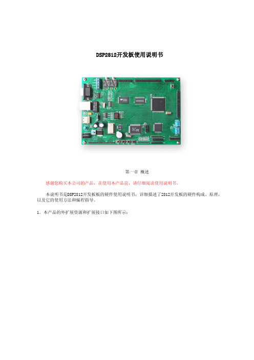
DSP2812开发板说明书
CANL 1 2 CANH
11.2812开发板的中断
F2812有3个中断引脚:XINT1,XINT2和XNMI_INT13,每个中断可配置为上升沿或下降沿触 发,也可以被使能或禁止。
开发板板上有8个外部中断源:
EXINT[1..4] 外部扩展总线可屏蔽的中断源
EXNMI[1..2] 外部扩展总线不可屏蔽的中断源
第三章 TMS320F2812的基本系统
1. 时钟电路
开发板用30MHz外部晶体给DSP提供时钟,并使能F2812 片上PLL电路。PLL倍频系数由PLL 控制寄存器PLLCR的低4位控制,可由软件动态的修改。外部复位信号(RS)可将此4位清零(CCS 中的复位命令将不能对这4位清零)。TMS320F2812的CPU最高可工作在150M的主频下,也即是 对30M输入频率进行5倍频。
TMS320F2812的外部存储器接口包括:19位地址线,16位数据线,3个片选控制线及读 写控制线。这3个片选线映射到5个存储区域,Zone0,Zone1,Zone2,Zone6和Zone7。其中, Zone0和Zone1共用1个片选线XCS0AND1,Zone6和Zone7共用1个片选线XCS6AND7。这5个存 储区域可分别设置不同的等待周期。
7. McBSP
开发板上有一个多通道缓冲型同步串口McBSP,在板上与AIC23的同步串口相连接。
8. SPI
开发板上有一个SPI同步串口,在板上与74HC595相连接。
9. SCI
开发板上有两个SCI异步串口,经485和232电平转换芯片连接到485CON和232CON,供外部使用。
10.CAN
开发板上有一个增强型的CAN总线控制器,符合CAN2.0B接口规范,经CAN收发器驱动后连接到 CANCON,提供外部使用。CANCON连接器定义如下:
基于单片机的健身器数据采集与分析系统设计
基于单片机的健身器数据采集与分析系统设计刘力1,杨光2,辛海会3,季怀军31.江苏省徐州医药高等职业学校,江苏徐州(221116)2.中国矿业大学计算机学院,江苏徐州(221116)3.中国矿业大学安全工程学院,江苏徐州(221116)E-mail: xinxhh@摘要:介绍了一种基于单片机的健身器数据采集与分析系统设计。
巧妙地综合了单片机技术,USB接口技术,Vsiual C++软件编程技术,实现了健身时身体机能各项指标及锻炼强度等数据的实时显示与长期保存,可以将数据上传到PC机上,通过PC机上友好界面对健身历史数据进行产看分析,使使系统简单实用。
健身者和专业医疗保健人员能根据历史数据跟好的了解健身者的身体健康状况并知道以后的锻炼方式。
该系统很具实际应用价值。
关键词:健身器;单片机;USB接口;MFC软件编程0 引言随着经济的目益发展,人们的生活水平在不断提高,同时用于健身的各种器械也迅速增加。
通过锻炼可以使身体各方面机能得到增强,同时在健身过程中,利用相关检测仪器所测得的身体各项参数能够反映锻炼时的身体健康状况。
而且将不同时期健身时所测得的身体各项指标数据经过统计,利用科学合理的医学手段分析出机体在一定时期内的总体健康状况以及变化趋势,这对保持机体健康具有指导性意义。
然而现在所使用的健身器材仅能显示健身时直接测得的各项数据,没有数据长期记忆功能和历史数据分析对比功能。
本文以AT89S52单片机为核心,开发了一套健身器数据采集与分析系统,其中数据采集与存储模块具有数据记录与显示功能,利用现在广泛应用的USB接口技术可以将已保存于存储模块中的数据上传到个人电脑上,在个人电脑上安装本系统的数据接受查看软件,这样健身者可以利用个人电脑查看自己一段时间内的锻炼情况及身体机能各项数据。
除此之外,可以将得到的历史数据发送给专业的医疗保健人员,进而方便快捷的对数据进行分析,从科学的角度掌握身体健康状况,达到指导以后的锻炼和保健的目的。
基于FPGA 的嵌入式系统设计

基于FPGA的嵌入式系统设计Design of Embedded System Based on FPGA(长江大学计算机科学学院) 林华Lin Hua摘要:提出了一种基于FPGA及MicroC /OS的嵌入式系统设计的新方法;从系统硬件平台设计与实现、系统软件配置、实时操作系统MicroC/OS-II的设计应用三方面详细介绍了整个系统平台的设计实现过程,并给出了验证结果。
关键字:FPGA;NIOS II;MicroC /OS;嵌入式系统中图分类号:TP 文献标识码:AAbstract:This paper proposes a new method for embedded system designing,based on FPGA and MicroC/OS.This paper introduce the design and realization course of the whole system flat in details from the hardware design,the software design and the design of MicroC/OS-II. the experiment result is given.Key words: FPGA;NIOS II;MicroC /OS;Embedded system1 前言近年来,随着嵌入式核心芯片的飞速发展,改变了传统嵌入式系统的设计方法,嵌入式系统逐渐由板级向芯片级过渡,即片上系统——SOC。
片上系统是追求产品系统最大包容的集成器件,是当前嵌入式应用领域的技术热点。
SOC的出现使集成电路发展成为集成系统,整个电子整机的功能可以集成到一块芯片中,降低了设计成本,缩短了开发周期。
因此,本文设计了一个基于FPGA的嵌入式系统,既能满足嵌入式系统教学实验的需要,同时也可作为嵌入式产品开发平台。
2 系统硬件设计本系统要实现的功能包括:可以运行嵌入式操作系统;支持NIOS II开发;支持USB 通讯;支持RS-232串口通讯;支持以太网通讯;支持JTAG接口在线调试与下载。
SL811HST资料
SL811HSSL811HSEmbedded USB Host/Slave ControllerTABLE OF CONTENTS1.0 CONVENTIONS (4)2.0 DEFINITIONS (4)3.0 REFERENCES (4)4.0 INTRODUCTION (4)4.1 Block Diagram (4)4.2 SL811HS Host or Slave Mode Selection [Master/Slave Mode] (5)4.3 Features (5)4.4 Data Port, Microprocessor Interface (6)4.5 Interrupt Controller (6)4.6 Buffer Memory (6)4.7 PLL Clock Generator (6)4.8 USB Transceiver (8)5.0 SL811HS REGISTERS (8)5.1 Register Values on Power-up and Reset (9)5.2 USB Control Registers (9)5.3 SL811HS Control Registers (12)6.0 SL811HS AND SL811HST-AC PHYSICAL CONNECTIONS (16)6.1 SL811HS Physical Connections (16)6.2 SL811HST-AC Physical Connections (19)7.0 ELECTRICAL SPECIFICATIONS (22)7.1 Absolute Maximum Ratings (22)7.2 Recommended Operating Condition (22)7.3 External Clock Input Characteristics (X1) (22)7.4 DC Characteristics (23)7.5 USB Host Transceiver Characteristics (23)7.6 Bus Interface Timing Requirements (24)8.0 PACKAGE DIAGRAMS (28)LIST OF FIGURESFigure 4-1. SL811HS USB Host/Slave Controller Functional Block Diagram (5)Figure 4-2. Full-Speed 48-MHz Crystal Circuit (7)Figure 4-3. Optional 12-MHz Crystal Circuit (7)Figure 6-1. SL811HS USB Host/Slave Controller—Pin Layout (16)Figure 6-2. SL811HST-AC USB Host/Slave Controller Pin Layout (19)LIST OF TABLESTable 6-1. SL811HS Pin Assignments and Definitions (17)Table 6-2. SL811HST-AC Pin Assignments and Definitions (20)License AgreementUse of this document and the intellectual properties contained herein indicates acceptance of the following License Agreement. If you do not accept the terms of this License Agreement, do not use this document, or the associated intellectual properties, or any other material you received in association with this product, and return this document and the associated materials within fifteen (15) days to Cypress Semiconductor Corporation or (CY) or CY’s authorized distributor from whom you purchased the product.1.You can only legally obtain CY’s intellectual properties contained in this document through CY or its authorized distributors.2.You are granted a nontransferable license to use and to incorporate CY’s intellectual properties contained in this documentinto your product. The product may be either for your own use or for sale.3.You may not reverse-engineer the SL811HS or otherwise attempt to discover the designs of SL811HS.4.You may not assign, distribute, sell, transfer or disclose CY’s intellectual properties contained in this document to any otherperson or entity.5.This license terminates if you fail to comply with any of the provisions of this Agreement. You agree upon termination to destroythis document, stop using the intellectual properties contained in this document and any of its modification and incorporated or merged portions in any form, and destroy any unused SL811HS chips.Warranty Disclaimer and Limited LiabilityCypress (CY), hereafter referred to as the manufacturer, warrants that its products substantially conform to its specifications for a period of ninety (90) days from delivery as evidenced by the shipment records. The manufacturer's sole obligation and liability for breaching the foregoing warranty shall be to replace or correct the defective products so that it substantially conforms to its specifications. Any modification of the products by anyone other than the manufacturer voids the foregoing warranty. No other warranties are expressed and none shall be implied. The manufacturer makes no warrant for the use of its products. In order to minimize risks associated with customer’s applications, adequate design and operating safeguards must be provided by the customer to minimize inherent or procedural hazards. The manufacturer’s products are not designed, authorized, or warranted suitable for use in life-support devices or systems or other critical applications. The manufacturer specifically excludes any implied warranties of merchantability and fitness for a particular purpose unless prohibited by law. In no event shall the manufacturer's liability to you for damages hereunder for any cause whatsoever exceed the amount paid by you for the products. In no event will the manufacturer be liable for any loss of profits or other incidental or consequential damages arising out of the use or inability to use the product even if the manufacturer have been advised of the possibility of such damages.The manufacturer reserves the right to make changes at any time, without notice, to improve design or performance and supply the best product possible. The manufacturer assumes no responsibility for any errors that may appear in its technical document on the products nor does it make a commitment to update the information contained in its technical document. Nothing contained in the technical documents of the products shall be construed as a recommendation to use any products in violation of existing patents, copyrights or other rights of third parties. No license is granted by implication or otherwise under any patent, patent rights or other rights, of the manufacturer.1.0 Conventions1,2,3,4Numbers without annotations are decimals.Dh, 1Fh, 39h Hexadecimal numbers are followed by an “h.”0101b, 010101b Binary numbers are followed by a “b.”bRequest, n Words in italics indicate terms defined by USB Specification or by this Specification.2.0 DefinitionsUSB U niversal S erial B usSL811HS The SL811HS is a Cypress USB Host/Slave Controller, providing multiple functions on a single chip.This part is offered in both a 28-pin PLCC package (SL811HS) and a 48-pin TQFP package(SL811HST-AC). Throughout this document, “SL811HS” refers to both packages unless otherwisenoted.Note: This chip does not include CPU.SL11The SL11 is a Cypress USB Peripheral Device Controller, providing multiple functions on a single chip.This part is offered in both a 28-pin PLCC package (SL11) and a 48-pin TQFP package (SL11T-AC).Throughout this document, “SL11” refers to both packages unless otherwise noted.Note: This chip does not include a CPU.SL11H The SL11H is a Cypress USB Host/Slave Controller, providing multiple functions on a single chip. This part is offered in both a 28-Pin PLCC package (SL11H) and a 48-Pin TQFP package (SL11HT-AC).Throughout this document, “SL11H” refers to both packages unless otherwise noted.Note: This chip does not include CPU.LSB L east S ignificant B itMSB M ost S ignificant B itR/W R ead/W ritePLL P hase L ock L oopRAM R andom A ccess M emorySIE S erial I nterface E ngineACK Handshake packet indicates a positive acknowledgment.NAK Handshake packet indicating a negative acknowledgmentUSBD U niversal S erial B us D riverSOF S tart o f F rame is the first transaction in each frame. It allows endpoints to identify the start of the frame and synchronize internal endpoint clocks to the host.CRC C yclic R edundancy C heckHOST The host computer system on which the USB Host Controller is installed3.0 References[Ref 1] USB Specification 1.1: .4.0 Introduction4.1Block DiagramThe SL811HS is an Embedded USB Host/Slave Controller capable of communicate with either full-speed or low-speed USB peripherals. The SL811HS can interface to devices such as microprocessors, microcontrollers, DSPs, or directly to a variety of buses such as ISA, PCMCIA, and others. The SL811HS USB Host Controller conforms to USB Specification 1.1.The SL811HS USB Host/Slave Controller incorporates USB Serial Interface functionality along with internal full-/low-speed trans-ceivers. The SL811HS supports and operates in USB full-speed mode at 12 Mbps, or at low-speed 1.5-Mbps mode.The SL811HS data port and microprocessor interface provide an 8-bit data path I/O or DMA bidirectional, with interrupt support to allow easy interface to standard microprocessors or microcontrollers such as Motorola or Intel CPUs and many others. Inter-nally, the SL811HS contains a 256-byte RAM data buffer which is used for control registers and data buffer.The available package types offered are a 28-pin PLCC (SL811HS) and a 48-pin TQFP package (SL811HST-AC). Both packages operate at 3.3 VDC. The I/O interface logic is 5V-tolerant.4.2SL811HS Host or Slave Mode Selection [Master/Slave Mode]SL811HS can work in two modes —host or slave. For slave-mode operation and specification, please refer to the SL811S specification. This data sheet only covers host-mode operation.4.3Features•The only USB Host/Slave controller for embedded systems in the market with a standard microprocessor bus interface.•Supports both full-speed (12 Mbps) and low-speed (1.5 Mbps) USB transfer 4.3.1USB Specification Compliance •Conforms to USB Specification 1.14.3.2CPU Interface•Operates as a single USB host or slave under software control•Low-speed 1.5 Mbps, and full speed 12 Mbps, in both master and slave modes •Automatic detection of either low- or full-speed devices•8-bit bidirectional data, port I/O (DMA supported in slave mode) •On-chip SIE and USB transceivers •On-chip single root HUB support•256-byte internal SRAM buffer, ping-pong operation•Operates from 12- or 48-MHz crystal or oscillator (built-in DPLL)•5 V-tolerant interface•Suspend/resume, wake up, and low-power modes are supported •Auto-generation of SOF and CRC5/16•Auto-address increment mode, saves memory Read/Write cycles •Development kit including source code drivers is available •Backward-compatible with SL11H, both pin and functionality •3.3V power source, 0.35 micron CMOS technology•Available in both a 28-pin PLCC package (SL811HS) and a 48-pin TQFP package (SL811HST-AC).D+D-GENERATORUSB Root-HUB XCVRS4.4Data Port, Microprocessor InterfaceThe SL811HS microprocessor interface provides an 8-bit bidirectional data path along with appropriate control lines to interface to external processors or controllers. The control lines, Chip Select, Read and Write input strobes and a single address line, A0, along with the 8-bit data bus, support programmed I/O or memory mapped I/O designs.Access to memory and control register space is a simple two step process, requiring an address Write with A0 set = “0,” followed by a register/memory Read or Write cycle with address line A0 set = “1.”In addition, DMA bidirectional interface in slave mode is available with handshake signals such as DREQ, ACK, WR, RD, CS and INTR. Please refer to the SL811S spec.The SL811HS Write or Read operation terminates when either nWR or nCS goes inactive. For devices interfacing to the SL811HS, that deactivate the Chip Select nCS before the Write nWR, the data hold timing should be measured from the nCS and will be the same value as specified. Thus, both Intel − and Motorola-type CPUs can work easily with the SL811HS without any external glue logic requirements.4.5Interrupt ControllerThe SL811HS interrupt controller provides a single output signal (INTRQ) that can be activated by a number of events that may occur as result of USB activity. Control and status registers are provided to allow the user to select single or multiple events, which will generate an interrupt (assert INTRQ), and lets the user view interrupt status. The interrupts can be cleared by writing to the appropriate register (the Status Register at address 0x0d).4.6Buffer MemoryThe SL811HS contains 256 bytes of internal buffer memory. The first 16 bytes of memory represent control and status registers for programmed I/O operations. The remaining memory locations are used for data buffering (max. 240 Bytes).Access to the registers and data memory is through an external microprocessor, 8-bit data bus, in either of two addressing modes, indexed or, if used with multiplexed address/data bus interfaces, direct access. With indexed addressing, the address is first written to the device with the A0 address line LOW, then the following cycle with A0 address line HIGH is directed to the specified address. USB transactions are automatically routed to the memory buffer. Control registers are provided, so that pointers and block sizes in buffer memory can be can set up.4.6.1Auto Address Increment ModeThe SL811HS supports auto-increment mode for Read or Write Cycles, A0 mode. In A0 mode, the Micro Controller sets up the address only once. On any subsequent DATA Read or Write access, the internal address pointer will advance to the next DATA location.4.6.1.1For exampleWrite 0x10 to SL811HS in address cycle (A0 is set LOW)Write 0x55 to SL811HS in data cycle (A0 is set HIGH) -> Write 0x55 to location 0x10Write 0xaa to SL811HS in data cycle (A0 is set HIGH) -> Write 0xaa to location 0x11Write 0xbb to SL811HS in data cycle (A0 is set HIGH) -> Write 0xbb to location 0x12The advantage of auto address increment mode is that it reduces the number of SL811HS memory Read/Write cycles required to move data to/from the device. For example, transferring 64-bytes of data to/from SL811HS using auto increment mode, will reduce the number of cycles to 1 Address Write and 64 Read/Write Data cycles, compared to 64 Address Writes and 64 Data Cycles for Random Access.4.7PLL Clock GeneratorEither a 12-MHz or a 48-MHz external crystal can be used with the SL811HS. Two pins, X1 and X2, are provided to connect a low-cost crystal circuit to the device as shown in Figure 4-2 and Figure 4-3. If an external 48-MHz clock source is available in the application, it can be used instead of the crystal circuit by connecting the source directly to the X1 input pin. When a clock is used, the X2 pin is left unconnected.Figure 4-2. Full-Speed 48-MHz Crystal CircuitFigure 4-3. Optional 12-MHz Crystal CircuitNote:1.CM (Clock Mode) pin of the SL811HS should be tied to GND when 48-MHz Xtal circuit or 48-MHz clock source is used.4.7.1Typical Crystal RequirementsThe following are examples of “typical requirements”. Please note that these specifications are generally found as standard crystal values and are therefore less expensive than custom values. If crystals are used in series circuits, load capacitance is not applicable. Load capacitance of parallel circuits is a requirement.12-MHz Crystals:Frequency Tolerance:±100 ppm or betterOperating Temperature Range:0°C to 70°CFrequency:12 MHzFrequency Drift over Temperature:± 50 ppmESR (Series Resistance):60ΩLoad Capacitance:10 pF min.Shunt Capacitance:7 pF max.Drive Level:0.1–0.5 mWOperating Mode:fundamental48-MHz Crystals:Frequency Tolerance:±100 ppm or betterOperating Temperature Range:0°C to 70°CFrequency:48 MHzFrequency Drift over Temperature:± 50 ppmESR (Series Resistance):40 ΩLoad Capacitance:10 pF min.Shunt Capacitance:7 pF max.Drive Level:0.1–0.5 mWOperating Mode:third overtone4.8USB TransceiverThe SL811HS has a built in transceiver that meets USB Specification 1.1. The transceiver is capable of transmitting and receiving serial data at USB full speed (12 Mbits) and low speed (1.5 Mbits). The driver portion of the transceiver is differential while the receiver section is comprised of a differential receiver and two single-ended receivers. Internally, the transceiver interfaces to the Serial Interface Engine (SIE) logic. Externally, the transceiver connects to the physical layer of the USB.5.0 SL811HS RegistersOperation of the SL811HS is controlled through 16 internal registers. A portion of the internal RAM is devoted to the control register space, and access is through the microprocessor interface. The registers provide control and status information for transactions on the USB, microprocessor interface, and interrupts.Any Write to control register 0FH will enable the SL811HS full features bit. This is an internal bit of the SL811HS that enables additional features not supported by the SL11H. For SL11H hardware backward compatibility, this register should not be accessed.The table below shows the memory map and register mapping of both the SL11H and SL811HS. The SL11H is shown for users upgrading to the SL811HS.The registers in the SL811HS are divided into two major groups. The first group is referred to as USB Control registers. These registers enable and provide status for control of USB transactions and data flow. The second group of registers provides control and status for all other operations.5.1Register Values on Power-up and ResetThe following registers initialize to zero on power-up and reset:•USB-A/USB-B Host Control Register [00H, 08H] bit 0 only •Control Register 1 [05H]•USB Address Register [07H]•Current Data Set/Hardware Revision/SOF Counter LOW Register [0EH]All other registers power-up and reset in an unknown state and should be initialized by firmware.5.2USB Control RegistersCommunication and data flow on the USB uses the SL811HS ’s USB A-B Control Registers. The SL811HS can communicate with any USB Device functions and any specific endpoints via the USBA or USBB register sets.The USB A-B Host Control Registers can be used in a Ping-Pong arrangement to manage traffic on the USB. The USB Host Control Register also provides a means to interrupt an external CPU or Micro Controller when one of the USB protocol transac-tions is completed. The table above shows the two sets of USB Host Control Registers, the “A ” set and “B ” set. The two register sets allow for overlapped operation. When one set of parameters is being set up, the other is transferring. On completion of a transfer to an endpoint, the next operation will be controlled by the other register set.Note . On the SL11H, the USB-B set control registers are not used. The USB-B register set can be used only when SL811HS mode is enabled by initializing register 0FH.The SL811HS USB Host Control has two groups of five registers each, which map in the SL811HS memory space. These registers are defined in the following tables.Register Name SL11H and SL811HSSL11H (hex)AddressSL811HS (hex)AddressUSB-A Host Control Register 00H 00H USB-A Host Base Address 01H 01H USB-A Host Base Length02H 02H USB-A Host PID, Device Endpoint (Write)/USB Status (Read)03H 03H USB-A Host Device Address (Write)/Transfer Count (Read)04H 04H Control Register105H 05H Interrupt Enable Register 06H 06 H Reserved RegisterReserved Reserved USB-B Host Control Register Reserved 08H USB-B Host Base Address Reserved 09H USB-B Host Base LengthReserved 0AH USB-B Host PID, Device Endpoint (Write)/USB Status (Read)Reserved 0BH USB-B Host Device Address (Write)/Transfer Count (Read)Reserved 0CH Status Register0DH 0DH SOF Counter LOW (Write)/HW Revision Register (Read)0EH 0E H SOF Counter HIGH and Control Register2Reserved 0F H Memory Buffer10H-FFH10H-FFH•Bit 3 is reserved for future usage.•The SL811HS uses bit 5 to enable transfer of a data packet after a SOF packet is transmitted. When this bit set “1,” the next enabled packet will be sent after next SOF. If set = “0” the next packet is sent immediately if the SIE is free.•The SL811HS automatically generates preamble packets when bit 7 is set. This bit is only used to send packets to a low-speed device through a hub. To communicate to a full speed device, this bit is set to zero. For example, when SL811HS communicates to a low-speed device via the HUB:—SL811HS SIE should set to operate at 48 MHz, i.e., bit 5 of register 05H should be set = “0.”—Bit 6 of register 0FH should be set = “0,” set correct polarity of DATA+ and DATA – state for Full Speed.—Bit 7, Preamble Bit, should be set = “1” in Host Control register.•When SL811HS communicates directly to low-speed device:—SL811HS. Bit 5 of register 05H should be set = “1.”—Bit 6 of register 0FH should be set = “1,” DATA+ and DATA – polarity for low speed.—The state of bit 7 is ignored in this mode.5.2.3Example of SL811HS USB Packet TransferSL811HS memory set-up as shown:03h-04h Register will contain PID and Device endpoint and Device Address.10h-FFh USB Data as required.5.2.1SL811HS Host Control RegistersRegister Name SL11H and SL811HSL11H (hex)AddressSL811HS (hex)AddressUSB-A Host Control Register 00H 00H USB-A Host Base Address 01H 01H USB-A Host Base Length02H 02H USB-A Host PID, Device Endpoint (Write)/USB Status (Read)03H 03H USB-A Host Device Address (Write)/Transfer Count (Read)04H 04H USB-B Host Control Register Reserved 08H USB-B Host Base Address Reserved 09H USB-B Host Base LengthReserved 0AH USB-B Host PID, Device Endpoint (Write)/USB Status (Read)Reserved 0BH USB-B Host Device Address (Write)/Transfer Count (Read)Reserved0CH5.2.2USB-A/USB-B Host Control Registers [00H, 08H]Bit PositionBit Name Function0Arm Allows enabled transfers when set = “1.” Cleared to “0” when transfer is complete.1Enable When set = “1” allows transfers to this endpoint. When set “0” USB transactions are ignored. If Enable = “1” and Arm = '0' the endpoint will return NAKs to USB transmissions. 2Direction When set = “1” transmit to Host. When “0” receive from Host.3Reserved 4ISO When set to “1” allows Isochronous mode for this endpoint.5SOF “1” = Synchronize with the SOF transfer 6Data Toggle Bit “0” if DATA0, “1” if DATA1.7PreambleIf set = “1” a preamble token is transmitted prior to transfer of low-speed packet. If set =“0,” preamble generation is disabled.5.2.4SOF Packet GenerationThe SL811HS automatically computes CRC5 by hardware. No CRC or SOF is required to be generated by external firmware for SL811HS.5.2.5USB-A/USB-B Host Base Address [01H, 09H]The USB-A/USB-B Base Address is a Pointer to the SL811HS memory buffer location for USB reads and writes. When trans-ferring data OUT (Host to Device), the USB-A and USB-B can be set up prior to setting ARM on the USB-A or USB-B Host Control register. See the software implementation example.5.2.6USB-A/USB-B Host Base Length [02H, 0AH]The USB A/B host base register contains the maximum packet size to be transferred between the SL811HS and a slave USB peripheral. Essentially, this designates the largest packet size that can be transferred by the SL811HS. Base Length designates the size of data packet to be sent. For example, in Bulk mode the maximum packet length is 64 bytes. In ISO mode, the maximum packet length is 1023, since the SL811HS only has an 8-bit length; the maximum packet size for the ISO mode using the SL811HS is 255 – 16 bytes. When the Host Base Length register is set to zero, a Zero-Length packet will be transferred.5.2.7USB-A/USB-B Host PID, Device Endpoint (Write)/USB Status (Read) [03H, 0BH]This register has two modes. When read, this register provides packet status and it contains information relative to the last packet that has been received or transmitted. The register is defined as follows.Bit Position Bit Name Function0ACK Transmission Acknowledge1Error Error detected in transmission2Time-out Time-out occurred3Sequence Sequence Bit. “0” if DATA0, “1” if DATA14Setup“1” indicates Setup Packet5Overflow Overflow condition - maximum length exceeded during receives6NAK Slave returns NAK7STALL Slave set STALL bitWhen written, this register provides the PID and Endpoint information to the USB SIE engine to be used in the next transaction. All sixteen Endpoints can be addressed by the SL811HS.D7D6D5D4D3D2D1D0PID3PID2PID1PID0EP3EP2EP1EP0PID3-04-bit PID Field (See Table Below)EP3-04-bit Endpoint Value in Binary.PID TYPE D7-D4SETUP1101 (D Hex)IN1001 (9 Hex)OUT0001 (1 Hex)SOF0101 (5 Hex)PREAMBLE1100 (C Hex)NAK1010 (A Hex)STALL1110 (E Hex)DATA00011 (3 Hex)DATA11011 (B Hex)5.2.8USB-A/USB-B Host Transfer Count Register (Read), USB Address (Write) [04H, 0CH]This register has two functions. When read, this register contains the number of bytes left over (from “Length” field) after a packet is transferred. If an overflow condition occurs, i.e., the received packet from slave USB device was greater than the Length field specified, a bit is set in the Packet Status Register indicating the condition. When written, this register will contain the USB Device Address to which the Host wishes to communicate.D7D6D5D4D3D2D1D00DA6DA5DA4DA3DA2DA1DA0DA6-DA0Device address, up to 127 devices can be addressedDA7Reserved bit should be set zero.5.3SL811HS Control RegistersRegister Name SL11H and SL811H SL11H (hex) Address SL811HS (hex) Address Control Register105H05HInterrupt Enable Register 06H06 HReserved Register 07H07 HStatus Register0DH0DHSOF Counter LOW (Write)/HW Revision Register (Read)0EH0E HSOF Counter HIGH and Control Register2Reserved0F HMemory Buffer10H-FFH10H-FFH5.3.1Control Register 1, Address [05H]The Control Register 05H enables/disables USB transfer operation with control bits defined as follows.Bit Bit Name Function0SOF ena/dis“1” enable auto Hardware SOF generation, “0”= disable1Reserved2Reserved3USB Engine Reset USB Engine reset = “1.” Normal set “0”4J-K state force See the table below5USB Speed“0” set-up for full speed, “1” set-up LOW-SPEED6Suspend “1” enable, “0” = disable7Reserved•At power-up this register will be cleared to all zeros.•In the SL811HS, bit 0 is used to enable HW SOF auto-generation (bit 0 was not used in the SL11H).5.3.2J-K Programming States [bits 3 and 4 of Control Register 05H]The J-K force state control and USB Engine Reset bits can be used to generate USB reset condition on the USB. Forcing K-state can be used for Peripheral device remote wake-up, Resume and other modes. These two bits are set to zero on power-up.5.3.3Low-speed/Full Speed Modes [bit 5 Control Register 05H]The SL811HS is designed to communicate with either full or low-speed devices. At power-up bit 5 will be set LOW, i.e., for full speed. There are two cases when communicating with a low-speed device. When a low-speed device is connected directly to the SL811HS, bit 5 of Register 05H should be set to logic “1” and bit 6 of register 0FH, Output-Invert, needs to be set to “1” in order to change the polarity of D+ and D –. When a low-speed device is connected via a HUB to SL811HS, bit 5 of Register 05H should be set to logic “0” and bit 6 of register 0FH should be set to logic “0” in order to keep the polarity of D+ and D – for full speed. In addition, make sure that bit 7 of USB-A/USB-B Host Control Registers [00H, 08H] is set to “1.”5.3.4Low-power Modes [bit 6 Control Register 05H]When bit-6 (Suspend) is set to “1,” the power of the transmit transceiver will be turned off, the internal RAM will be in the suspend mode, and the internal clocks will be disabled. Note . Any activity on the USB bus (i.e., K-State, etc.) will resume normal operation.To resume normal operation from the CPU side, a data Write cycle (i.e., A0 set HIGH for a data Write cycle) should be done.5.3.5Interrupt Enable Register, Address [06H]The SL811HS provides an Interrupt Request Output, which can be activated on a number of conditions. The Interrupt Enable Register allows the user to select conditions that will result in an Interrupt being issued to an external CPU. A separate Interrupt Status Register is provided. It can be polled in order to determine those conditions that initiated the interrupt. (See Interrupt Status Register description.) When a bit is set to “1” the corresponding interrupt is enabled.•Bits 0–1 are used for the USB A/B controller interrupt.•Bit 4 is used to enable/disable the SOF timer. To utilize this bit function, bit 0 of register 05H must be enabled and the SOF counter registers 0EH and 0FH must be initialized.•Bit 5 is used to enable/disable the device inserted/removed interrupt.•When bit-6 of register 05H is set = “1,” bit 6 of this register enables the Resume Detect Interrupt. Otherwise, this bit is used to enable Device detection status as defined in the Interrupt Status Register bit definitions.Note:2.Force K-State for low speed.3.Force J-State for low speed.Bit 4Bit 3Function00Normal operating mode01Force USB Reset, D+ and D – are set LOW (SE0)10Force J-State, D+ set HIGH, D – set LOW [2]11Force K-State, D – set HIGH, D+ set LOW [3]Bit PositionBit Name Function0USB-A USB-A Done Interrupt 1USB-B USB-B Done Interrupt2Reserved 3Reserved 4SOF Timer 1 = Enable Interrupt on 1-ms SOF Timer 5Inserted/Removed Slave Insert/Remove Detection 6Device Detect/ResumeEnable Device Detect/Resume Interrupt。
Curriculum design
题目一:ARM平台与PC间的通讯设计要求:ARM平台与PC间通讯包括三个方面:(1)基于Socket的通讯程序设计;(2)基于串口是RS232的通讯程序设计;(3)基于USB的串行通讯程序设计。
给出系统设计题目二:ARM中断系统分析设计要求:从软、硬件的角度分析ARM系统中的异常中断类型、功能及特点,并给出中断处理的方法、流程及相关中断程序实现。
题目三:Bootloader引导装载器分析设计要求:对Bootloader源代码进行分析,画出bootloader流程图,并在bootloader中实现网卡驱动和串口驱动。
题目四:嵌入式WEB服务器实现设计要求:基于ARM实验板上设计并实现一个web服务器。
题目五:LCD驱动程序设计与实现设计要求:基于QT或miniGUI进行。
题目六:A/D转换器驱动程序设计设计要求:利用Linux内核提供的重要函数接口,结合S3C2410内部A/D转换器,设计并实现Linux 下A/D转换驱动程序的设计。
基于ARM 嵌入式XML 文档解析器设计方案1 概述该系统通过USB 接口接收PC 机发过来的XML 的文档,然后解析并在液晶屏上显示出来。
用户通过键盘输入相关信息后,生成相应的XML 文档,再通过USB 口从终端传回PC 机。
2 体系结构设计图1 体系结构框图2.1硬件体系结构设计:图2 硬件框图本系统的硬件核心是三星公司ARM 处理器44B0,它具有强大的实时处理能力和丰富的外围接口,外部扩展1片2M的SDRAM(HY57V641620)、一片8MB的NAND Flash和一片2MB NOR FLASH(SST39LF160)存储器,构成最小ARM应用系统。
外围扩展USB模块(ARM7采用Cypress公司的SL811HS芯片具有主/从两种工作模式的USB控制器,遵循USB1.1规范),显示液晶模块(3.8英寸16级灰度STN LCD, 分辨率为320×240,240×128,128×64),以及4*4矩阵键盘输入模块。
SL811HS开发板原理图
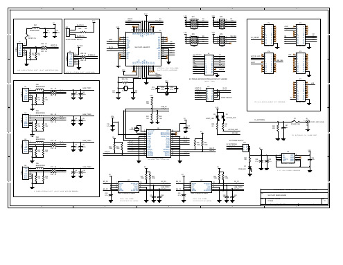
CYPRESS USB DUAL-SPEED HOST/SLAVE CONTROLLER D0 INTRQ nRST
Female_10x2
Female_10x2
R19 1M 3.3V
C
E X TERNAL MICROCONTROLLER DEV KIT HEADER (Male 10x2)
P1 1 3 5 7 9 11 13 15 17 19 2 4 6 8 10 12 14 16 18 20 nCS
3.3V 5V FB1 JP2 BLM41P800S
D
P5 1 2 3 4 5 6 7 8 9 10 11 12 13 14 15 16 17 18 19 20 Female_10x2 nWR 5V_DEVKIT
P3 1 2 3 4 5 6 7 8 9 10 11 12 13 14 15 16 17 18 19 20 Female_10x2
B
Female_10x2
3.3V
HUB_PWR2 3.3V C5 0.1u + C6 220u R21 15K R22 15K 5V
D3 HOST_LED
D4 ACTIVE_LED 5V_EXTERNAL F2 1 +5V DC JACK (2.5A) R33 20K ACTIVE_LED MS_SEL 5V EXTERNAL DC POWER INPUT + C27 22u 2,3 3216FF-2.5A J4
5
4
3
2
1
3.3V 3.3V nDACK nDRQ nRD 3.3V 48 47 46 45 44 43 42 41 40 39 38 37 R40 1K5 U1 3.3V RP2 NC NC NC D6 D5 D4 GND D3 D2 D1 NC NC 36 35 34 33 32 31 30 29 28 27 26 25 1 2 3 4 100K 8 7 6 5 D3 D4 D5 D6 1 2 3 4 100K 100K 3.3V RP4 8 7 6 5 MS_SEL nDACK nRST 5V_DEVKIT 100K A0 MS_SEL D7 1 2 3 4 RP1 8 7 6 5 A0 D0 D1 D2 3.3V 1 2 3 4 RP3 8 7 6 5 D7 nRD nCS nWR
基于SL811HS的嵌入式USB主控制器接口设计
d v c e uma in wee ito c d. Th ou in wh c a e n m o te b d d s se i i e,eay t e i pe e e e ie n to r n rdu e e s lto ih c n beus d i s m e de y t m ssmpl s o b m lm ntd
t tr g a a a o c mmunc t t m b d e y t ms o so a e d t nd t o ia ewih e e d d s se .
Ke r s L 1 ywo d :S 8 HS;u ieslsra b s( B);e e d d;US otpoo o 1 nv ra eil u US mbd e B h s rtcl
软件 的开 发 要 求 较 高 ; O I 把 较 多 的 功 能 定 义 ③ HC 则
在硬件 中 , 软件 需要处 理 的 内容 相对 较少 , 对系统 的处
起 来 。U B凭借其 接 口简单 、 插 即用 、 输 速 率 高 、 S 即 传 易于扩展 等优 点 , 渐 有 替 代 普 通 接 口的趋 势 。 随着 逐 越 来越 多的 U B设 备 在 日常 生 活 和工 作 研 究 中 的普 S
及, 嵌入 式设 备急需 提供 对这 些设 备 的支持 。
本 研 究 通 过 采 用 U B 主 机 功 能 芯 片 为 高 性 能 S
理 能力 和 系统 资 源 的 要求 较 低 。 因此 , 嵌 入式 U B 在 S 主机 开发 中 , 多地选 用遵 循 O I 范 的硬件 , 而 较 HC 规 从
D e i n o m b dd d U S h s o r le nt r a e b e sg f e e e B o t c nt o lr i e f c as d on SL81 S 1 H
DEV硬件说明

DEV_3210硬件说明1、概述DEV_3210是一款基于高性能处理器Soc 3210i 设计实现的方案。
该方案采用的Soc 3210i 是高集成度系统级芯片,主频可达266MHz 。
在DEV_3210板面上集成了SDRAM 、Nand Flash 和各种外围设备 包括RJ-45网口、音频输入与输出、SD-CARD 接口,Jtag 接口,USB 接口、标准串口、LCD 接口,P/S2(鼠标键盘接口),GPIO 接口等。
整个硬件结构如下图所示3、硬件特性1 CPU Soc 3210i ,主频最高可达266MHz2 FLASH2M NOR FLASH ,最大支持8M NOR FLASH ,同时支持256M NAND FLASH 存储器3 SDRAM 64M 内存4 LCD数字TFT ,用TRULY 3.5实现,同时支持模拟VGA ,通过权电阻网络/VGA 芯片实现5 网络 一个10/100M 以太网接口6 SERIAL 一个DB9 Male 标准串口7 AUDIO 一路MIC 输入,两路音频输出 8 JATG 一个标准的14针JATG 接口9 POWER 12V 电源10 SD 卡 一个SD 卡卡槽,SPI接口 11 PS/2 鼠标键盘标准接口各一个 12 IDC插座 25X2.0插座13 红外接收头 一个红外接收头,接收距离10米左右 4、板载资源说明 母板板载资源RTL8201BLSDRAM SDRAM IC6 IC7ALC203E 7408*5红外接收头J3 TRULY LCD SOCKETJ4 SHARPLCD SOCKET箭头所指的为第一脚5.2母板+外壳RTL8201SDRAM7408*5SDRAMTSC20036、模块以及接口说明6.1 电源供电系统的设计在嵌入式产品的设计中至关重要,工程师不但需要考虑电源本身的基本电气参数,还要考虑电源的稳定性设计。
本设计中的电源使用的为AP1513和AMS117开关稳压芯片,它具有纹波小、高效以及出色的瞬时响应的特性,为系统提供+5V、+3.3V和+1.8V的稳定电压。
在单片机上实现USB移动存储
在单片机上实现USB移动存储第1章主要硬件芯片介绍1.1系统总体设计USB主机系统设计是一个软、硬件结合的整体,宏观上主要包括三个层次的设计:USB总线物理层接口设计、USB核心系统设计和USB客户系统设计。
总线接口主要处理主机与设备之间的电气及协议层的互连,是信息包进出的物理桥梁;USB核心系统主要管理和协调主机与从机间的逻辑数据传输,解析双方联系的握手协议,是验证信息包的逻辑关卡;客户系统是最终用户直接和USB设备功能交互的逻辑平台,不同的USB设备归属于不同的类,是利用相关的类协议来实现的,所以客户系统驱动程序具有多变性,需要为专门的类定制专门的驱动程序。
在单片机上实现USB移动存储功能,具体包括USB主机接口的硬件设计和整机USB驱动固件的设计。
其中驱动固件的设计具体又包含几个协议的实现:USB1.1控制传输协议、USB BULK传输协议、USB海量存储类协议、UFI磁盘操作命令和FAT文件系统标准等。
1.2硬件设计1.2.1USB主控制器USB主控制器主要是完成底层物理接口设计,是US B系统架构的必要部分,是USB数据包进出的必经通道。
本系统采用的USB主机芯片是Cypress公司的SL811HS。
Cypr ess公司是最早从事USB芯片开发的公司之一,其EZ-USB系列芯片在业界有非常好的口碑。
SL811HS是当经第一个支持USB 主从机的接口芯片,性能稳定,资料全面。
(1)芯片特性SL811HS是自动兼容USB全速或者低速的嵌入式U SB主从机的接口芯片,它支持微处理器、微控制器或者DSP的USB接口设计,同时也可以直接连到ISA、PCMIC A等其它总线[8],芯片使用标准的USB1.1协议。
SL81 1HS通过内部集成的全/低速传输引擎产生USB串行接口功能,在全速时带宽为12Mbps,低速时为1.5Mbps。
芯片支持8位并行数据端口或者I/O口的设计,同时也支持DMA,自动中断检测连接口,可以非常容易地在MCS-51系列微处理器、摩托罗拉微控制器或者其它控制芯片上完成设计。
51单片机控制SL811HS的USB主机底层驱动
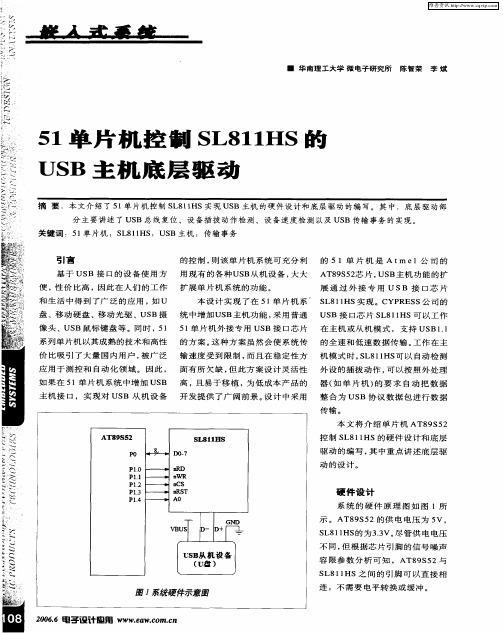
20. 0 66电 子 设 计 匝 用 W .口 t m.n WW e w. o c
维普资讯
S L81 HS 内部 指 令 周 期 的 大小 将 直 接 影 响 输 出信 1
子 程 序 模 块 枚 举 设 备 层 次 关 系 最 高 层 寄 存 器
对于输出传输事务单片机同样需要设置相关的寄存器以确定标表3一个传输事务的数据流示意表4与传输事务直接相关的sl811hs特殊寄存器嵌入式系统嵌入式系统111electronicdesignapplicationworldnikkeielectronicschina记包的标识域地址域端点域和数据包的标识域以及存放发送数据的缓冲区首地址并且这个缓冲区中的数据也是由单片机写具体地单片机控制usb主机接口芯片进行一次传输事务所需要执行的操作步骤如下
r 二
0
摘 要 :本 文 介 绍 了 5 单 片 机 控 制 S 8 1 l L 1 HS实现 US 主 机 的硬 件 设 计和 底 层 驱 动 的编 写 。其 中 ,底 层 驱 动 部 B 分 主要 讲 述 了 US 总线 复 位 、设 备 插 拔 动 作 检 测 、设 备 速 度 检 测 以及 US B B传 输 事 务 的实现 。 关 键 词 :5 1单 片机 ;S 1HS;US L8 1 B主机 中增 加 US 高 ,且 易 于 移 植 ,为 低 成 本 产 品 的 器 ( 单 片 机 ) 要 求 自 动 把 数 据 B 如 的
主 机 接 口 , 实 现 对 US 从 机 设 备 开 发 提 供 了 广 阔 前 景 。 计 中采 用 B 设
整 合 为 US B协 议 数 据 包 进 行 数 据 传输。
引 言
的 控 制 , 该 单 片 机 系 统 可 充分 利 的 51 单 片 机 是 A I l公 司 的 则 tT e I
USB接口技术及驱动程序开发

的设备驱动程序需要有“即插即用(PnP)”模块以及安装标识的INF文件。
在上述不同模块之间需要交互,其中的一些交互可以直接通过函数调用,而大量信息需要通过数据结构传递(比如在”设备对象”之类的数据结构中可以存储每个设备的信息)。
IRP,每个设备对象有一个内部的IRP队列,驱动程序的分发例程把1RP插入到这个设备队列中,内核I/O管理器从该队列一个个取出IRP,并传递到驱动程序的Startlo例程,Startlo例程串行处理IRP,以确保不与其它IRP处理程序冲突,但是StartIo例程仍然需要通过临界段例程避免与硬件中断发生冲突。
中断是用于停止处理器对一个任务的执行,而被强制运行某个中断去处理代码。
中断包括软件中断和硬件中断。
中断具有优先级,低优先级中断会被高优先级的中断所中断,以保证重要任务会优先执行。
硬件产生的中断总是比软件产生的中断优先级要高。
硬件中断类型包括:设备中断请求级处理程序的执行、配置文件定时器、时钟、同步器、处理器之间中断级、电源故障级;软件中断包括异步过程调用执行、线程调度、延迟过程调用执行。
至于常规线程执行则没有中断。
基本驱动程序例程Ifo控制伊腰派遣规程必须的驱动程序例程处理请求队列聪包含戳artlo_【蹙备产生中断需要包舍中断服务和OPc洲程DMA设备需要包含AdapterContro橱腥可选的l刚书R遣例程图3-2WDM设备驱动程序的模块组驱动程序的主要的初始化入口点是一个称为DriverEntry的例程。
多数WDM设备对象是由PIlP管理器调用AddDevice入15点创建,该例程在插入新设备和安装INF文件指示相对应的驱动程序时被调用,之后,一系列P11PIRP被发送到。
基于SL811HS的单片机扩展USB接口设计

于丹 张专成 矫佳 妮 武警工程学院通信工 程系
弓言 |
动计算机 ,用户可将 U盘插到 P C机
单 片机选 用 AT L公 司生产 ME
位单片机 A 8 S 2 T 9 5 ,它与 目前 ,在工 控机 、嵌 入式 系统 中 ,便 可直接对采集 到 的数据进行 的高性能 8 S5 1系列产 品的指令 和引脚完 中,数据采集和交换 大多使用 软盘 、 分 析 处 理 +从 而 极 大 的 方便 了 用 Mc 一 全兼 容 ,片 内集成 有 8 F s B l k a h 串行接 n和以太网等方式。由于软盘 户 。
OT S S T 速传输速度为 1M p ,即使是低速模 H S 接 口控制器则用来控制 U B总 两种 封 装 形 式 , 内含 u B H0S / bs 2 LV 式, 其传输速度也可达 1 M p , . bs 而最 线接 口与 U盘进行命令 和数据交换 ; SA E控制器 ,支持全速( l sed/ 5 f l pe) u— A 1 —p e ) n 新的 U B . S 20协议则 支持 的最高传输 高速 R M用于数据缓 冲,以在传输数 低速( w sed数据传输 ,并能 自动 速度可达到 4 0 b s 8 M p ,非常适合于大 据文件时做文件系统的缓存 区用 。 容量数据传输的系统 。U B设备支持 S
基 于S 8 1 S L 1 H 的单 片机读写u 的系统 实现方法, 盘 该方法可解决在便携式仪器或 嵌入式 系统上外挂海量存储设备的问题。 文中重点分析 了系统的原理及传输协议 . HS L 1 ;AT 9 5 ;U盘 1 8S2
述领域 的数据存储和交换提供了新的 阔 的 用 前 景 。
它是整个 系统 的核心 ,主要完 成主
可能性 ,这种技术可 以实现快速 、低
基于单片机的USB接口的设计
基于单片机的USB接口的设计
刘井权;王宪;戴旻
【期刊名称】《自动化仪表》
【年(卷),期】2006(027)008
【摘要】提出了一种基于单片机的智能仪表扩展USB接口的方法.介绍了USB接口芯片SL811HS的结构和性能以及USB接口的硬件电路图,详细分析了USB接口驱动程序的设计方法及FAT16文件系统的结构.利用SCSI传输命令集,通过BULK-IN和BULK-OUT端点实现了主机与U盘设备之间的数据通信.实验和应用结果表明,该方案具有控制方便、传输速度快、存储数据稳定可靠等优点.
【总页数】3页(P29-31)
【作者】刘井权;王宪;戴旻
【作者单位】江南大学通信与控制工程学院,无锡,214122;江南大学通信与控制工程学院,无锡,214122;江南大学通信与控制工程学院,无锡,214122
【正文语种】中文
【中图分类】TP368
【相关文献】
1.基于USB接口的51单片机在线编程设计 [J], 陈志英
2.基于AVR单片机与USB接口的多道谱仪的设计 [J], 吉晓梅;刘志珍;郭星辰;李玮瑛;张培旭
3.基于AT89C5131单片机和CPLD的USB接口用户专用键盘设计 [J], 张鑫;张庆力;周吉
4.基于51单片机和PDIUSB12的USB接口设计 [J], 张学峰;陈瑾;翟从鸿;彭文超;朱家俊
5.基于USB接口的微机与单片机通信系统设计 [J], 王海军
因版权原因,仅展示原文概要,查看原文内容请购买。
- 1、下载文档前请自行甄别文档内容的完整性,平台不提供额外的编辑、内容补充、找答案等附加服务。
- 2、"仅部分预览"的文档,不可在线预览部分如存在完整性等问题,可反馈申请退款(可完整预览的文档不适用该条件!)。
- 3、如文档侵犯您的权益,请联系客服反馈,我们会尽快为您处理(人工客服工作时间:9:00-18:30)。
SL811HSSL811HSEmbedded USB Host/Slave ControllerTABLE OF CONTENTS1.0 CONVENTIONS (4)2.0 DEFINITIONS (4)3.0 REFERENCES (4)4.0 INTRODUCTION (4)4.1 Block Diagram (4)4.2 SL811HS Host or Slave Mode Selection [Master/Slave Mode] (5)4.3 Features (5)4.4 Data Port, Microprocessor Interface (6)4.5 Interrupt Controller (6)4.6 Buffer Memory (6)4.7 PLL Clock Generator (6)4.8 USB Transceiver (8)5.0 SL811HS REGISTERS (8)5.1 Register Values on Power-up and Reset (9)5.2 USB Control Registers (9)5.3 SL811HS Control Registers (12)6.0 SL811HS AND SL811HST-AC PHYSICAL CONNECTIONS (16)6.1 SL811HS Physical Connections (16)6.2 SL811HST-AC Physical Connections (19)7.0 ELECTRICAL SPECIFICATIONS (22)7.1 Absolute Maximum Ratings (22)7.2 Recommended Operating Condition (22)7.3 External Clock Input Characteristics (X1) (22)7.4 DC Characteristics (23)7.5 USB Host Transceiver Characteristics (23)7.6 Bus Interface Timing Requirements (24)8.0 PACKAGE DIAGRAMS (28)LIST OF FIGURESFigure 4-1. SL811HS USB Host/Slave Controller Functional Block Diagram (5)Figure 4-2. Full-Speed 48-MHz Crystal Circuit (7)Figure 4-3. Optional 12-MHz Crystal Circuit (7)Figure 6-1. SL811HS USB Host/Slave Controller—Pin Layout (16)Figure 6-2. SL811HST-AC USB Host/Slave Controller Pin Layout (19)LIST OF TABLESTable 6-1. SL811HS Pin Assignments and Definitions (17)Table 6-2. SL811HST-AC Pin Assignments and Definitions (20)License AgreementUse of this document and the intellectual properties contained herein indicates acceptance of the following License Agreement. If you do not accept the terms of this License Agreement, do not use this document, or the associated intellectual properties, or any other material you received in association with this product, and return this document and the associated materials within fifteen (15) days to Cypress Semiconductor Corporation or (CY) or CY’s authorized distributor from whom you purchased the product.1.You can only legally obtain CY’s intellectual properties contained in this document through CY or its authorized distributors.2.You are granted a nontransferable license to use and to incorporate CY’s intellectual properties contained in this documentinto your product. The product may be either for your own use or for sale.3.You may not reverse-engineer the SL811HS or otherwise attempt to discover the designs of SL811HS.4.You may not assign, distribute, sell, transfer or disclose CY’s intellectual properties contained in this document to any otherperson or entity.5.This license terminates if you fail to comply with any of the provisions of this Agreement. You agree upon termination to destroythis document, stop using the intellectual properties contained in this document and any of its modification and incorporated or merged portions in any form, and destroy any unused SL811HS chips.Warranty Disclaimer and Limited LiabilityCypress (CY), hereafter referred to as the manufacturer, warrants that its products substantially conform to its specifications for a period of ninety (90) days from delivery as evidenced by the shipment records. The manufacturer's sole obligation and liability for breaching the foregoing warranty shall be to replace or correct the defective products so that it substantially conforms to its specifications. Any modification of the products by anyone other than the manufacturer voids the foregoing warranty. No other warranties are expressed and none shall be implied. The manufacturer makes no warrant for the use of its products. In order to minimize risks associated with customer’s applications, adequate design and operating safeguards must be provided by the customer to minimize inherent or procedural hazards. The manufacturer’s products are not designed, authorized, or warranted suitable for use in life-support devices or systems or other critical applications. The manufacturer specifically excludes any implied warranties of merchantability and fitness for a particular purpose unless prohibited by law. In no event shall the manufacturer's liability to you for damages hereunder for any cause whatsoever exceed the amount paid by you for the products. In no event will the manufacturer be liable for any loss of profits or other incidental or consequential damages arising out of the use or inability to use the product even if the manufacturer have been advised of the possibility of such damages.The manufacturer reserves the right to make changes at any time, without notice, to improve design or performance and supply the best product possible. The manufacturer assumes no responsibility for any errors that may appear in its technical document on the products nor does it make a commitment to update the information contained in its technical document. Nothing contained in the technical documents of the products shall be construed as a recommendation to use any products in violation of existing patents, copyrights or other rights of third parties. No license is granted by implication or otherwise under any patent, patent rights or other rights, of the manufacturer.1.0 Conventions1,2,3,4Numbers without annotations are decimals.Dh, 1Fh, 39h Hexadecimal numbers are followed by an “h.”0101b, 010101b Binary numbers are followed by a “b.”bRequest, n Words in italics indicate terms defined by USB Specification or by this Specification.2.0 DefinitionsUSB U niversal S erial B usSL811HS The SL811HS is a Cypress USB Host/Slave Controller, providing multiple functions on a single chip.This part is offered in both a 28-pin PLCC package (SL811HS) and a 48-pin TQFP package(SL811HST-AC). Throughout this document, “SL811HS” refers to both packages unless otherwisenoted.Note: This chip does not include CPU.SL11The SL11 is a Cypress USB Peripheral Device Controller, providing multiple functions on a single chip.This part is offered in both a 28-pin PLCC package (SL11) and a 48-pin TQFP package (SL11T-AC).Throughout this document, “SL11” refers to both packages unless otherwise noted.Note: This chip does not include a CPU.SL11H The SL11H is a Cypress USB Host/Slave Controller, providing multiple functions on a single chip. This part is offered in both a 28-Pin PLCC package (SL11H) and a 48-Pin TQFP package (SL11HT-AC).Throughout this document, “SL11H” refers to both packages unless otherwise noted.Note: This chip does not include CPU.LSB L east S ignificant B itMSB M ost S ignificant B itR/W R ead/W ritePLL P hase L ock L oopRAM R andom A ccess M emorySIE S erial I nterface E ngineACK Handshake packet indicates a positive acknowledgment.NAK Handshake packet indicating a negative acknowledgmentUSBD U niversal S erial B us D riverSOF S tart o f F rame is the first transaction in each frame. It allows endpoints to identify the start of the frame and synchronize internal endpoint clocks to the host.CRC C yclic R edundancy C heckHOST The host computer system on which the USB Host Controller is installed3.0 References[Ref 1] USB Specification 1.1: .4.0 Introduction4.1Block DiagramThe SL811HS is an Embedded USB Host/Slave Controller capable of communicate with either full-speed or low-speed USB peripherals. The SL811HS can interface to devices such as microprocessors, microcontrollers, DSPs, or directly to a variety of buses such as ISA, PCMCIA, and others. The SL811HS USB Host Controller conforms to USB Specification 1.1.The SL811HS USB Host/Slave Controller incorporates USB Serial Interface functionality along with internal full-/low-speed trans-ceivers. The SL811HS supports and operates in USB full-speed mode at 12 Mbps, or at low-speed 1.5-Mbps mode.The SL811HS data port and microprocessor interface provide an 8-bit data path I/O or DMA bidirectional, with interrupt support to allow easy interface to standard microprocessors or microcontrollers such as Motorola or Intel CPUs and many others. Inter-nally, the SL811HS contains a 256-byte RAM data buffer which is used for control registers and data buffer.The available package types offered are a 28-pin PLCC (SL811HS) and a 48-pin TQFP package (SL811HST-AC). Both packages operate at 3.3 VDC. The I/O interface logic is 5V-tolerant.4.2SL811HS Host or Slave Mode Selection [Master/Slave Mode]SL811HS can work in two modes —host or slave. For slave-mode operation and specification, please refer to the SL811S specification. This data sheet only covers host-mode operation.4.3Features•The only USB Host/Slave controller for embedded systems in the market with a standard microprocessor bus interface.•Supports both full-speed (12 Mbps) and low-speed (1.5 Mbps) USB transfer 4.3.1USB Specification Compliance •Conforms to USB Specification 1.14.3.2CPU Interface•Operates as a single USB host or slave under software control•Low-speed 1.5 Mbps, and full speed 12 Mbps, in both master and slave modes •Automatic detection of either low- or full-speed devices•8-bit bidirectional data, port I/O (DMA supported in slave mode) •On-chip SIE and USB transceivers •On-chip single root HUB support•256-byte internal SRAM buffer, ping-pong operation•Operates from 12- or 48-MHz crystal or oscillator (built-in DPLL)•5 V-tolerant interface•Suspend/resume, wake up, and low-power modes are supported •Auto-generation of SOF and CRC5/16•Auto-address increment mode, saves memory Read/Write cycles •Development kit including source code drivers is available •Backward-compatible with SL11H, both pin and functionality •3.3V power source, 0.35 micron CMOS technology•Available in both a 28-pin PLCC package (SL811HS) and a 48-pin TQFP package (SL811HST-AC).D+D-GENERATORUSB Root-HUB XCVRS4.4Data Port, Microprocessor InterfaceThe SL811HS microprocessor interface provides an 8-bit bidirectional data path along with appropriate control lines to interface to external processors or controllers. The control lines, Chip Select, Read and Write input strobes and a single address line, A0, along with the 8-bit data bus, support programmed I/O or memory mapped I/O designs.Access to memory and control register space is a simple two step process, requiring an address Write with A0 set = “0,” followed by a register/memory Read or Write cycle with address line A0 set = “1.”In addition, DMA bidirectional interface in slave mode is available with handshake signals such as DREQ, ACK, WR, RD, CS and INTR. Please refer to the SL811S spec.The SL811HS Write or Read operation terminates when either nWR or nCS goes inactive. For devices interfacing to the SL811HS, that deactivate the Chip Select nCS before the Write nWR, the data hold timing should be measured from the nCS and will be the same value as specified. Thus, both Intel − and Motorola-type CPUs can work easily with the SL811HS without any external glue logic requirements.4.5Interrupt ControllerThe SL811HS interrupt controller provides a single output signal (INTRQ) that can be activated by a number of events that may occur as result of USB activity. Control and status registers are provided to allow the user to select single or multiple events, which will generate an interrupt (assert INTRQ), and lets the user view interrupt status. The interrupts can be cleared by writing to the appropriate register (the Status Register at address 0x0d).4.6Buffer MemoryThe SL811HS contains 256 bytes of internal buffer memory. The first 16 bytes of memory represent control and status registers for programmed I/O operations. The remaining memory locations are used for data buffering (max. 240 Bytes).Access to the registers and data memory is through an external microprocessor, 8-bit data bus, in either of two addressing modes, indexed or, if used with multiplexed address/data bus interfaces, direct access. With indexed addressing, the address is first written to the device with the A0 address line LOW, then the following cycle with A0 address line HIGH is directed to the specified address. USB transactions are automatically routed to the memory buffer. Control registers are provided, so that pointers and block sizes in buffer memory can be can set up.4.6.1Auto Address Increment ModeThe SL811HS supports auto-increment mode for Read or Write Cycles, A0 mode. In A0 mode, the Micro Controller sets up the address only once. On any subsequent DATA Read or Write access, the internal address pointer will advance to the next DATA location.4.6.1.1For exampleWrite 0x10 to SL811HS in address cycle (A0 is set LOW)Write 0x55 to SL811HS in data cycle (A0 is set HIGH) -> Write 0x55 to location 0x10Write 0xaa to SL811HS in data cycle (A0 is set HIGH) -> Write 0xaa to location 0x11Write 0xbb to SL811HS in data cycle (A0 is set HIGH) -> Write 0xbb to location 0x12The advantage of auto address increment mode is that it reduces the number of SL811HS memory Read/Write cycles required to move data to/from the device. For example, transferring 64-bytes of data to/from SL811HS using auto increment mode, will reduce the number of cycles to 1 Address Write and 64 Read/Write Data cycles, compared to 64 Address Writes and 64 Data Cycles for Random Access.4.7PLL Clock GeneratorEither a 12-MHz or a 48-MHz external crystal can be used with the SL811HS. Two pins, X1 and X2, are provided to connect a low-cost crystal circuit to the device as shown in Figure 4-2 and Figure 4-3. If an external 48-MHz clock source is available in the application, it can be used instead of the crystal circuit by connecting the source directly to the X1 input pin. When a clock is used, the X2 pin is left unconnected.Figure 4-2. Full-Speed 48-MHz Crystal CircuitFigure 4-3. Optional 12-MHz Crystal CircuitNote:1.CM (Clock Mode) pin of the SL811HS should be tied to GND when 48-MHz Xtal circuit or 48-MHz clock source is used.4.7.1Typical Crystal RequirementsThe following are examples of “typical requirements”. Please note that these specifications are generally found as standard crystal values and are therefore less expensive than custom values. If crystals are used in series circuits, load capacitance is not applicable. Load capacitance of parallel circuits is a requirement.12-MHz Crystals:Frequency Tolerance:±100 ppm or betterOperating Temperature Range:0°C to 70°CFrequency:12 MHzFrequency Drift over Temperature:± 50 ppmESR (Series Resistance):60ΩLoad Capacitance:10 pF min.Shunt Capacitance:7 pF max.Drive Level:0.1–0.5 mWOperating Mode:fundamental48-MHz Crystals:Frequency Tolerance:±100 ppm or betterOperating Temperature Range:0°C to 70°CFrequency:48 MHzFrequency Drift over Temperature:± 50 ppmESR (Series Resistance):40 ΩLoad Capacitance:10 pF min.Shunt Capacitance:7 pF max.Drive Level:0.1–0.5 mWOperating Mode:third overtone4.8USB TransceiverThe SL811HS has a built in transceiver that meets USB Specification 1.1. The transceiver is capable of transmitting and receiving serial data at USB full speed (12 Mbits) and low speed (1.5 Mbits). The driver portion of the transceiver is differential while the receiver section is comprised of a differential receiver and two single-ended receivers. Internally, the transceiver interfaces to the Serial Interface Engine (SIE) logic. Externally, the transceiver connects to the physical layer of the USB.5.0 SL811HS RegistersOperation of the SL811HS is controlled through 16 internal registers. A portion of the internal RAM is devoted to the control register space, and access is through the microprocessor interface. The registers provide control and status information for transactions on the USB, microprocessor interface, and interrupts.Any Write to control register 0FH will enable the SL811HS full features bit. This is an internal bit of the SL811HS that enables additional features not supported by the SL11H. For SL11H hardware backward compatibility, this register should not be accessed.The table below shows the memory map and register mapping of both the SL11H and SL811HS. The SL11H is shown for users upgrading to the SL811HS.The registers in the SL811HS are divided into two major groups. The first group is referred to as USB Control registers. These registers enable and provide status for control of USB transactions and data flow. The second group of registers provides control and status for all other operations.5.1Register Values on Power-up and ResetThe following registers initialize to zero on power-up and reset:•USB-A/USB-B Host Control Register [00H, 08H] bit 0 only •Control Register 1 [05H]•USB Address Register [07H]•Current Data Set/Hardware Revision/SOF Counter LOW Register [0EH]All other registers power-up and reset in an unknown state and should be initialized by firmware.5.2USB Control RegistersCommunication and data flow on the USB uses the SL811HS ’s USB A-B Control Registers. The SL811HS can communicate with any USB Device functions and any specific endpoints via the USBA or USBB register sets.The USB A-B Host Control Registers can be used in a Ping-Pong arrangement to manage traffic on the USB. The USB Host Control Register also provides a means to interrupt an external CPU or Micro Controller when one of the USB protocol transac-tions is completed. The table above shows the two sets of USB Host Control Registers, the “A ” set and “B ” set. The two register sets allow for overlapped operation. When one set of parameters is being set up, the other is transferring. On completion of a transfer to an endpoint, the next operation will be controlled by the other register set.Note . On the SL11H, the USB-B set control registers are not used. The USB-B register set can be used only when SL811HS mode is enabled by initializing register 0FH.The SL811HS USB Host Control has two groups of five registers each, which map in the SL811HS memory space. These registers are defined in the following tables.Register Name SL11H and SL811HSSL11H (hex)AddressSL811HS (hex)AddressUSB-A Host Control Register 00H 00H USB-A Host Base Address 01H 01H USB-A Host Base Length02H 02H USB-A Host PID, Device Endpoint (Write)/USB Status (Read)03H 03H USB-A Host Device Address (Write)/Transfer Count (Read)04H 04H Control Register105H 05H Interrupt Enable Register 06H 06 H Reserved RegisterReserved Reserved USB-B Host Control Register Reserved 08H USB-B Host Base Address Reserved 09H USB-B Host Base LengthReserved 0AH USB-B Host PID, Device Endpoint (Write)/USB Status (Read)Reserved 0BH USB-B Host Device Address (Write)/Transfer Count (Read)Reserved 0CH Status Register0DH 0DH SOF Counter LOW (Write)/HW Revision Register (Read)0EH 0E H SOF Counter HIGH and Control Register2Reserved 0F H Memory Buffer10H-FFH10H-FFH•Bit 3 is reserved for future usage.•The SL811HS uses bit 5 to enable transfer of a data packet after a SOF packet is transmitted. When this bit set “1,” the next enabled packet will be sent after next SOF. If set = “0” the next packet is sent immediately if the SIE is free.•The SL811HS automatically generates preamble packets when bit 7 is set. This bit is only used to send packets to a low-speed device through a hub. To communicate to a full speed device, this bit is set to zero. For example, when SL811HS communicates to a low-speed device via the HUB:—SL811HS SIE should set to operate at 48 MHz, i.e., bit 5 of register 05H should be set = “0.”—Bit 6 of register 0FH should be set = “0,” set correct polarity of DATA+ and DATA – state for Full Speed.—Bit 7, Preamble Bit, should be set = “1” in Host Control register.•When SL811HS communicates directly to low-speed device:—SL811HS. Bit 5 of register 05H should be set = “1.”—Bit 6 of register 0FH should be set = “1,” DATA+ and DATA – polarity for low speed.—The state of bit 7 is ignored in this mode.5.2.3Example of SL811HS USB Packet TransferSL811HS memory set-up as shown:03h-04h Register will contain PID and Device endpoint and Device Address.10h-FFh USB Data as required.5.2.1SL811HS Host Control RegistersRegister Name SL11H and SL811HSL11H (hex)AddressSL811HS (hex)AddressUSB-A Host Control Register 00H 00H USB-A Host Base Address 01H 01H USB-A Host Base Length02H 02H USB-A Host PID, Device Endpoint (Write)/USB Status (Read)03H 03H USB-A Host Device Address (Write)/Transfer Count (Read)04H 04H USB-B Host Control Register Reserved 08H USB-B Host Base Address Reserved 09H USB-B Host Base LengthReserved 0AH USB-B Host PID, Device Endpoint (Write)/USB Status (Read)Reserved 0BH USB-B Host Device Address (Write)/Transfer Count (Read)Reserved0CH5.2.2USB-A/USB-B Host Control Registers [00H, 08H]Bit PositionBit Name Function0Arm Allows enabled transfers when set = “1.” Cleared to “0” when transfer is complete.1Enable When set = “1” allows transfers to this endpoint. When set “0” USB transactions are ignored. If Enable = “1” and Arm = '0' the endpoint will return NAKs to USB transmissions. 2Direction When set = “1” transmit to Host. When “0” receive from Host.3Reserved 4ISO When set to “1” allows Isochronous mode for this endpoint.5SOF “1” = Synchronize with the SOF transfer 6Data Toggle Bit “0” if DATA0, “1” if DATA1.7PreambleIf set = “1” a preamble token is transmitted prior to transfer of low-speed packet. If set =“0,” preamble generation is disabled.5.2.4SOF Packet GenerationThe SL811HS automatically computes CRC5 by hardware. No CRC or SOF is required to be generated by external firmware for SL811HS.5.2.5USB-A/USB-B Host Base Address [01H, 09H]The USB-A/USB-B Base Address is a Pointer to the SL811HS memory buffer location for USB reads and writes. When trans-ferring data OUT (Host to Device), the USB-A and USB-B can be set up prior to setting ARM on the USB-A or USB-B Host Control register. See the software implementation example.5.2.6USB-A/USB-B Host Base Length [02H, 0AH]The USB A/B host base register contains the maximum packet size to be transferred between the SL811HS and a slave USB peripheral. Essentially, this designates the largest packet size that can be transferred by the SL811HS. Base Length designates the size of data packet to be sent. For example, in Bulk mode the maximum packet length is 64 bytes. In ISO mode, the maximum packet length is 1023, since the SL811HS only has an 8-bit length; the maximum packet size for the ISO mode using the SL811HS is 255 – 16 bytes. When the Host Base Length register is set to zero, a Zero-Length packet will be transferred.5.2.7USB-A/USB-B Host PID, Device Endpoint (Write)/USB Status (Read) [03H, 0BH]This register has two modes. When read, this register provides packet status and it contains information relative to the last packet that has been received or transmitted. The register is defined as follows.Bit Position Bit Name Function0ACK Transmission Acknowledge1Error Error detected in transmission2Time-out Time-out occurred3Sequence Sequence Bit. “0” if DATA0, “1” if DATA14Setup“1” indicates Setup Packet5Overflow Overflow condition - maximum length exceeded during receives6NAK Slave returns NAK7STALL Slave set STALL bitWhen written, this register provides the PID and Endpoint information to the USB SIE engine to be used in the next transaction. All sixteen Endpoints can be addressed by the SL811HS.D7D6D5D4D3D2D1D0PID3PID2PID1PID0EP3EP2EP1EP0PID3-04-bit PID Field (See Table Below)EP3-04-bit Endpoint Value in Binary.PID TYPE D7-D4SETUP1101 (D Hex)IN1001 (9 Hex)OUT0001 (1 Hex)SOF0101 (5 Hex)PREAMBLE1100 (C Hex)NAK1010 (A Hex)STALL1110 (E Hex)DATA00011 (3 Hex)DATA11011 (B Hex)5.2.8USB-A/USB-B Host Transfer Count Register (Read), USB Address (Write) [04H, 0CH]This register has two functions. When read, this register contains the number of bytes left over (from “Length” field) after a packet is transferred. If an overflow condition occurs, i.e., the received packet from slave USB device was greater than the Length field specified, a bit is set in the Packet Status Register indicating the condition. When written, this register will contain the USB Device Address to which the Host wishes to communicate.D7D6D5D4D3D2D1D00DA6DA5DA4DA3DA2DA1DA0DA6-DA0Device address, up to 127 devices can be addressedDA7Reserved bit should be set zero.5.3SL811HS Control RegistersRegister Name SL11H and SL811H SL11H (hex) Address SL811HS (hex) Address Control Register105H05HInterrupt Enable Register 06H06 HReserved Register 07H07 HStatus Register0DH0DHSOF Counter LOW (Write)/HW Revision Register (Read)0EH0E HSOF Counter HIGH and Control Register2Reserved0F HMemory Buffer10H-FFH10H-FFH5.3.1Control Register 1, Address [05H]The Control Register 05H enables/disables USB transfer operation with control bits defined as follows.Bit Bit Name Function0SOF ena/dis“1” enable auto Hardware SOF generation, “0”= disable1Reserved2Reserved3USB Engine Reset USB Engine reset = “1.” Normal set “0”4J-K state force See the table below5USB Speed“0” set-up for full speed, “1” set-up LOW-SPEED6Suspend “1” enable, “0” = disable7Reserved•At power-up this register will be cleared to all zeros.•In the SL811HS, bit 0 is used to enable HW SOF auto-generation (bit 0 was not used in the SL11H).5.3.2J-K Programming States [bits 3 and 4 of Control Register 05H]The J-K force state control and USB Engine Reset bits can be used to generate USB reset condition on the USB. Forcing K-state can be used for Peripheral device remote wake-up, Resume and other modes. These two bits are set to zero on power-up.5.3.3Low-speed/Full Speed Modes [bit 5 Control Register 05H]The SL811HS is designed to communicate with either full or low-speed devices. At power-up bit 5 will be set LOW, i.e., for full speed. There are two cases when communicating with a low-speed device. When a low-speed device is connected directly to the SL811HS, bit 5 of Register 05H should be set to logic “1” and bit 6 of register 0FH, Output-Invert, needs to be set to “1” in order to change the polarity of D+ and D –. When a low-speed device is connected via a HUB to SL811HS, bit 5 of Register 05H should be set to logic “0” and bit 6 of register 0FH should be set to logic “0” in order to keep the polarity of D+ and D – for full speed. In addition, make sure that bit 7 of USB-A/USB-B Host Control Registers [00H, 08H] is set to “1.”5.3.4Low-power Modes [bit 6 Control Register 05H]When bit-6 (Suspend) is set to “1,” the power of the transmit transceiver will be turned off, the internal RAM will be in the suspend mode, and the internal clocks will be disabled. Note . Any activity on the USB bus (i.e., K-State, etc.) will resume normal operation.To resume normal operation from the CPU side, a data Write cycle (i.e., A0 set HIGH for a data Write cycle) should be done.5.3.5Interrupt Enable Register, Address [06H]The SL811HS provides an Interrupt Request Output, which can be activated on a number of conditions. The Interrupt Enable Register allows the user to select conditions that will result in an Interrupt being issued to an external CPU. A separate Interrupt Status Register is provided. It can be polled in order to determine those conditions that initiated the interrupt. (See Interrupt Status Register description.) When a bit is set to “1” the corresponding interrupt is enabled.•Bits 0–1 are used for the USB A/B controller interrupt.•Bit 4 is used to enable/disable the SOF timer. To utilize this bit function, bit 0 of register 05H must be enabled and the SOF counter registers 0EH and 0FH must be initialized.•Bit 5 is used to enable/disable the device inserted/removed interrupt.•When bit-6 of register 05H is set = “1,” bit 6 of this register enables the Resume Detect Interrupt. Otherwise, this bit is used to enable Device detection status as defined in the Interrupt Status Register bit definitions.Note:2.Force K-State for low speed.3.Force J-State for low speed.Bit 4Bit 3Function00Normal operating mode01Force USB Reset, D+ and D – are set LOW (SE0)10Force J-State, D+ set HIGH, D – set LOW [2]11Force K-State, D – set HIGH, D+ set LOW [3]Bit PositionBit Name Function0USB-A USB-A Done Interrupt 1USB-B USB-B Done Interrupt2Reserved 3Reserved 4SOF Timer 1 = Enable Interrupt on 1-ms SOF Timer 5Inserted/Removed Slave Insert/Remove Detection 6Device Detect/ResumeEnable Device Detect/Resume Interrupt。