CD5333B中文资料
FAN5333ASX;FAN5333BSX;FAN5333SX;中文规格书,Datasheet资料

FAN5333A/FAN5333B High Efficiency, High Current Serial LED Driver with 30V Integrated SwitchFAN5333A/FAN5333B High Efficiency, High Current Serial LED Driver with 30V Integrated SwitchFAN5333A/FAN5333B High Efficiency, High Current Serial LED Driver with 30V Integrated Switch Absolute Maximum Ratings (Note1)Recommended Operating Conditions Notes:1.Stresses above those listed under “Absolute Maximum Ratings” may cause permanent damage to the device. This is a stress rating only and functional operation of the device at these or any other conditions above those indicated in the operational section of this specification is not implied. Exposure to absolute maximum rating conditions for extended periods may affect device reliability. Absolute maximum ratings apply individually only, not in ing EIA/JESD22A114B (Human Body Model) and EIA/JESD22C101-A (Charge Device Model).3.This load capacitance value is required for the loop stability. Tolerance, temperature variation, and voltage dependency of the capacitance must be considered. Typically a 1µF ceramic capacitor is required to achieve specified value at V OUT = 30V.Parameter Min Max Unit V IN to GND 6.0V FB, SHDN to GND-0.3V IN + 0.3V SW to GND-0.335V Lead Soldering T emperature (10 seconds)300°C Junction T emperature150°C Storage T emperature-55150°C Thermal Resistance (ΘJA)210°C/W Electrostatic Discharge Protection (ESD) Level (Note 2)HBM2kV CDM1Parameter Min Typ Max Unit Input Voltage 1.8 5.5V Output Voltage V IN30V Operating Ambient T emperature-402585°C Output Capacitance Rated at the Required Output (Note 3) for maximum load current 0.47µFFAN5333A/FAN5333B High Efficiency, High Current Serial LED Driver with 30V Integrated SwitchFAN5333A/FAN5333B High Efficiency, High Current Serial LED Driver with 30V Integrated SwitchFAN5333A/FAN5333B High Efficiency, High Current Serial LED Driver with 30V Integrated Switch Time (100µs/div)L = 10µH C IN = 10µF C OUT = 1µF V IN = 2.7VFAN5333A/FAN5333B High Efficiency, High Current Serial LED Driver with 30V Integrated SwitchFAN5333A/FAN5333B High Efficiency, High Current Serial LED Driver with 30V Integrated SwitchFAN5333A/FAN5333B High Efficiency, High Current Serial LED Driver with 30V Integrated SwitchFAN5333A/FAN5333B High Efficiency, High Current Serial LED Driver with 30V Integrated Switch分销商库存信息:FAIRCHILDFAN5333ASX FAN5333BSX FAN5333SX。
SMBG5333B中文资料
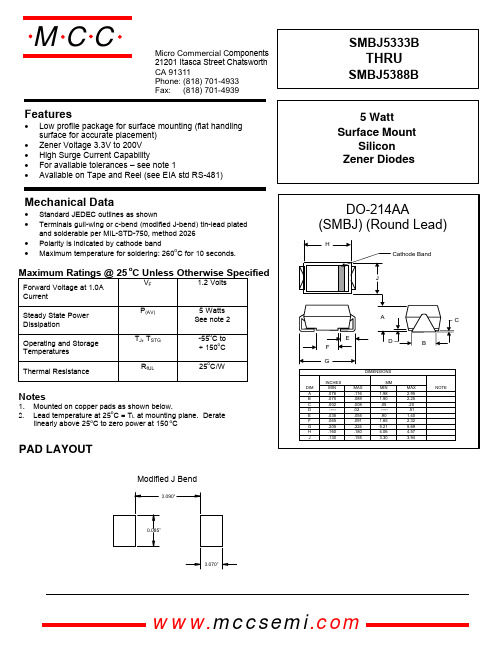
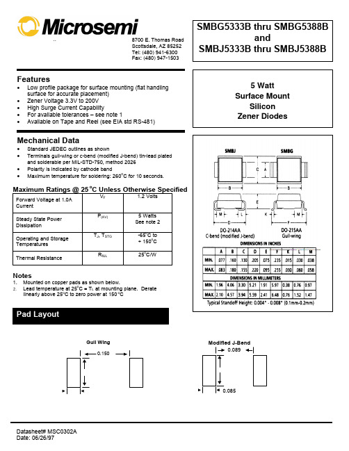
Features• Low profile package for surface mounting (flat handlingsurface for accurate placement)• Zener Voltage 3.3V to 200V • High Surge Current Capability• For available tolerances – see note 1• Available on Tape and Reel (see EIA std RS-481)Mechanical Data• Standard JEDEC outlines as shown• Terminals gull-wing or c-bend (modified J-bend) tin-lead platedand solderable per MIL-STD-750, method 2026• Polarity is indicated by cathode band• Maximum temperature for soldering: 260oC for 10 seconds.Maximum Ratings @ 25o C Unless Otherwise SpecifiedForward Voltage at 1.0A CurrentV F1.2 VoltsSteady State Power DissipationP (AV)5 Watts See note 2Operating and Storage Temperatures T J , T STG -55o C to+ 150oC Thermal ResistanceR θJL25o C/WNotes1. Mounted on copper pads as shown below.2. Lead temperature at 25o C = T L at mounting plane. Deratelinearly above 25o C to zero power at 150 oC0.070”0.090"0.085”Modified J BendPAD LAYOUTomp onents 21201 Itasca Street Chatsworth! "# $ % ! "#Features• Low profile package for surface mounting (flat handlingsurface for accurate placement)• Zener Voltage 3.3V to 200V • High Surge Current Capability• For available tolerances – see note 1• Available on Tape and Reel (see EIA std RS-481)Mechanical Data• Standard JEDEC outlines as shown• Terminals gull-wing or c-bend (modified J-bend) tin-lead platedand solderable per MIL-STD-750, method 2026• Polarity is indicated by cathode band• Maximum temperature for soldering: 260oC for 10 seconds.Maximum Ratings @ 25o C Unless Otherwise SpecifiedForward Voltage at 1.0A CurrentV F1.2 VoltsSteady State Power DissipationP (AV)5 Watts See note 2Operating and Storage Temperatures T J , T STG -55oC to+ 150oC Thermal ResistanceR θJL25o C/WNotes1. Mounted on copper pads as shown below.2. Lead temperature at 25o C = T L at mounting plane. Deratelinearly above 25o C to zero power at 150 oC! "# $ % ! "#0.070”0.190"0.125”Gull WingPAD LAYOUTMicrosemiPart Number RegulatorVoltage(V Z)TestCurrent(I ZT)MaximumDynamicImpedance(Z Z)(A&B Suffix)MaximumReverseCurrent(I R)@ V RI R TestVoltage(V R)(Non-Suffix& A Suffix)I R TestVoltage(V R)(B,C,DSuffix)MaximumRegulatorCurrent(I ZM)(B,C,D Suffix)MaximumDynamicKneeImpedanceZ zk @ 1.0 mA(A,B,C,D Suffix)MaximumSurgeCurrent(I ZSM)MaximumVoltageRegulation(∆V Z)(A,B,C,DSuffix)Gull-WingLeadC-Bend(Mod – J)V mAdc OHMSµA V V mA OHMS AMPS VOLTSSMBG5333B SMBG5334B SMBG5335B SMBG5336B SMBG5337B SMBJ5333BSMBJ5334BSMBJ5335BSMBJ5336BSMBJ5337B3.33.63.94.34.73803503202902603.02.52.02.02.030015050105.01.01.01.01.01.01.01.01.01.01.0144013201220110010104005005005004502018.717.616.415.30.850.800.540.490.44SMBG5338B SMBG5339B SMBG5340B SMBG5341B SMBG5342B SMBJ5338BSMBJ5339BSMBJ5340BSMBJ5341BSMBJ5342B5.15.66.06.26.82402202002001751.51.01.01.01.01.01.01.01.0101.02.03.03.04.91.02.03.03.05.293086579076570040040030020020014.413.412.712.411.50.390.250.190.100.15SMBG5343B SMBG5344B SMBG5345B SMBG5346B SMBG5347B SMBJ5343BSMBJ5344BSMBJ5345BSMBJ5346BSMBJ5347B7.58.28.79.1101751501501501251.51.52.02.02.01010107.55.06.46.96.256.67.25.76.26.66.97.663058054552047520020020015012510.7109.59.28.60.150.200.200.220.22SMBG5348B SMBG5349B SMBG5350B SMBG5351B SMBG5352B SMBJ5348BSMBJ5349BSMBJ5350BSMBJ5351BSMBJ5352B1112131415125100100100752.52.52.52.52.55.02.01.01.01.08.08.69.410.110.88.49.19.910.611.543039526534031512512510075758.07.57.06.76.30.250.250.250.250.25SMBG5353B SMBG5354B SMBG5355B SMBG5356B SMBG5357B SMBJ5353BSMBJ5354BSMBJ5355BSMBJ5356BSMBJ5357B161718192075706565652.52.52.53.03.01.00.50.50.50.511.512.21313.714.412.212.313.714.415.229528026425023775757575756.05.85.55.35.10.300.350.400.400.40SMBG5358B SMBG5359B SMBG5360B SMBG5361B SMBG5362B SMBJ5358BSMBJ5359BSMBJ5360BSMBJ5361BSMBJ5362B222425272850505050503.53.54.05.06.00.50.50.50.50.515.817.31819.420.116.718.21920.621.2216198190176170751001101201304.74.44.34.13.90.450.550.550.600.60SMBG5363B SMBG5364B SMBG5365B SMBG5366B SMBG5367B SMBJ5363BSMBJ5364BSMBJ5365BSMBJ5366BSMBJ5367B303336394340403030308.0101114200.50.50.50.50.521.623.825.928.13122.825.127.429.732.71581441321221101401501601701903.73.53.33.12.80.600.630.650.650.70SMBG5368B SMBG5369B SMBG5370B SMBG5371B SMBG5372B SMBJ5368BSMBJ5369BSMBJ5370BSMBJ5371BSMBJ5372B4751566062252520202025273540420.50.50.50.50.533.836.740.34344.635.838.842.545.547.1100938679762102302803504002.72.52.32.22.10.800.901.001.201.35SMBG5373B SMBG5374B SMBG5375B SMBG5376B SMBG5377B SMBJ5373BSMBJ5374BSMBJ5375BSMBJ5376BSMBJ5377B6875828791202015151544456575750.50.50.50.50.54954596365.551.75662.26669.270635854.552.55006207207607602.01.91.81.71.61.501.601.802.002.20SMBG5378B SMBG5379B SMBG5380B SMBG5381B SMBG5382B SMBJ5378BSMBJ5379BSMBJ5380BSMBJ5381BSMBJ5382B100110120130140121210108.0901251701902300.50.50.50.50.57279.286.493.61017683.691.293.810647.54339.536.63480010001150125015001.51.41.31.21.22.302.502.502.502.50SMBG5383B SMBG5384B SMBG5385B SMBG5386B SMBG5387B SMBG5388B SMBJ5383BSMBJ5384BSMBJ5385BSMBJ5386BSMBJ5387BSMBJ5388B1501601701801902008.08.08.05.05.05.03303503804304504800.50.50.50.50.50.510811512213013714411412212913714415231.529.42826.42523.61500166017501750185018501.11.11.01.00.90.93.003.003.004.005.005.00Electrical CharacteristicsNote 1Devices listed have a ± 5% tolerance on nominal V Z.The suffix A denotes a ± 20% tolerance, suffix Cdenotes ± 2%, and suffix D denotes ± 1%.Note 2Nominal Zener Voltage (V Z) is read with the device in standard test clips with 3/8 to ½ inch spacing betweenclip and case of the diode. Before reading, the diode isallowed so stabilize for a period of 40 ± 10 millisecondsat 25°C (+8, -2°C).Note 3The Zener impedance (Z ZT or Z ZK is derived from the 60H Z ac voltage, which results when an ac current havinga rms value equal to 10% of the dc zener current (I ZT orI ZK) is superimposed on I ZT or I ZK respectively. Dynamicimpedance variations with other current values aredescribed in Micronote 202.Note 4The Maximum Reverse (leakage) Current is specified for devices with ± 20% and ± 10% voltage toleranceson nominal V Z in another column.Note 5The Maximum Zener Current (I ZM) shown is for ± 5% tolerance devices. I ZM for ± 10% and ± 20% devicescan be calculated using the formula:I ZM = PV ZMWhere “V ZM” is V Z at the high end of the voltagetolerance specified and “P” is the rated power of thedevice.Note 6The Surge Current (I ZM) is specified as the maximum peak of a nonrecurring sine wave of 8.3 millisecondsduration.Note 7Voltage Regulation (∆V Z) is the difference between the voltage measured at 10% and 50% I ZM).。
CD4031B中文资料

IMPORTANT NOTICETexas Instruments and its subsidiaries (TI) reserve the right to make changes to their products or to discontinue any product or service without notice, and advise customers to obtain the latest version of relevant information to verify, before placing orders, that information being relied on is current and complete. All products are sold subject to the terms and conditions of sale supplied at the time of order acknowledgement, including those pertaining to warranty, patent infringement, and limitation of liability.TI warrants performance of its semiconductor products to the specifications applicable at the time of sale in accordance with TI’s standard warranty. Testing and other quality control techniques are utilized to the extent TI deems necessary to support this warranty. Specific testing of all parameters of each device is not necessarily performed, except those mandated by government requirements.CERTAIN APPLICATIONS USING SEMICONDUCTOR PRODUCTS MAY INVOLVE POTENTIAL RISKS OF DEATH, PERSONAL INJURY, OR SEVERE PROPERTY OR ENVIRONMENTAL DAMAGE (“CRITICAL APPLICATIONS”). TI SEMICONDUCTOR PRODUCTS ARE NOT DESIGNED, AUTHORIZED, OR WARRANTED TO BE SUITABLE FOR USE IN LIFE-SUPPORT DEVICES OR SYSTEMS OR OTHER CRITICAL APPLICATIONS. INCLUSION OF TI PRODUCTS IN SUCH APPLICATIONS IS UNDERSTOOD TO BE FULLY AT THE CUSTOMER’S RISK.In order to minimize risks associated with the customer’s applications, adequate design and operating safeguards must be provided by the customer to minimize inherent or procedural hazards.TI assumes no liability for applications assistance or customer product design. TI does not warrant or represent that any license, either express or implied, is granted under any patent right, copyright, mask work right, or other intellectual property right of TI covering or relating to any combination, machine, or process in which such semiconductor products or services might be or are used. TI’s publication of information regarding any third party’s products or services does not constitute TI’s approval, warranty or endorsement thereof.Copyright © 1998, Texas Instruments Incorporated。
CDB5330A中文资料

Features•Demonstrates recommended layoutand grounding arrangements•CS8402A Generates AES/EBU, S/PDIF,& EIAJ-340 Compatible Digital Audio•Buffered Serial Output Interface •Digital and Analog Patch Areas•On-board or externally supplied systemtimingGeneral DescriptionThe CDB5330A/31A evaluation board is an excellent means for quickly evaluating the CS5330A/31A 18-bit,stereo A/D converter. Evaluation requires a digital signal processor, a low distortion analog signal source and a power supply. Analog inputs are pro-vided via RCA connectors for both channels.Also included is a CS8402A digital audio interface transmitter which generates AES/EBU, S/PDIF, and EIAJ-340 compatible audio data. The digital audio data is available via RCA phono, and optical connectors.The evaluation board may also be configured to accept external timing signals for operation in a user applica-tion during system development.ORDERING INFORMATION: CDB5330A, CDB5331AEvaluation Board for CS5330A / CS5331ACDB5330A CDB5331ACirrus Logic, Inc.Crystal Semiconductor Product Division P.O. Box 17847, Austin, TX 78760(512) 445-7222 FAX: (512) 445-7581OCT ’97DS138DB217Copyright © Cirrus Logic, Inc. 1997(All Rights Reserved)CDB5330A/31A System OverviewThe CDB5330A/31A evaluation board is an ex-cellent means of quickly evaluating the CS5330A/31A. The CS8402A digital audio in-terface transmitter provides an easy interface to digital audio signal processors, including the ma-jority of digital audio test equipment. The evaluation board has been designed to accept an analog input, and provide a digital output that is either optical or coax. The evaluation board also allows the user to supply clocks and data through a 10-pin header for system development. The CDB5330A/31A schematic has been parti-tioned into 5 schematics shown in Figures 2 through 6. Each partitioned schematic is repre-sented in the system diagram shown in Figure 1. Notice that the the system diagram also includes the interconnections between the partitioned schematics.CS5330A/31A Analog to Digital ConverterA description of the CS5330A/31A is included in the CS5330A/31A data sheet.CS8402A Digital Audio InterfaceFigure 4 shows the CS8402A circuitry which implements AES/EBU, S/PDIF and EIAJ CP-340 digital audio interface standards. The CS8402A circuit is hardware configured for con-sumer mode. SW2 provides 8 DIP switches to select various modes and bits for the CS8402A, Tables 4-5. See the CS8401A/CS8402A data sheet for detailed information on the operation of the CS8402A and the digital audio standards. The operation of the CS8402A and a discussion of the digital audio interface are included in the 1994 Crystal Semiconductor Audio Data Book. CS8402A Data FormatThe CS8402A data format can be set with jump-ers M0, M1, and M2. These formats are shown in the CS8402A datasheet found in the 1994 Crystal Semiconductor Audio Data Book. The format selected must be compatible with the cor-responding data format of the CS5330A/31A shown in Figures 2 and 3 of the CS5330A/31A datasheet. The default settings for M0-M2 on the evaluation board are given in Tables 2 and 3. The compatible data formats for the CS8402A and CS5330A/31A are:CS8402A format 1;CS5330ACS8402A format 4;CS5331AAnalog input bufferThe recommended input filter required for the CS5330A/31A has been combined with a unity gain input buffer (see Figure 2). The analog in-put filter uses a Motorola MC33202 single supply, dual op-amp.Power Supply CircuitryPower is supplied to the evaluation board by two binding posts (GND, +5V), Figure 6. The +5V input supplies power to the +5 V olt digital cir-cuitry (VD+), and the +5V analog circuitry (V A+). The analog supply is derived from the +5V binding post through a ferrite bead.Input/Output for Clocks and DataThe evaluation board has been designed to allow the interface to external systems via the 10-pin CLOCK I/O header, HDR2. This header allows the evaluation board to accept externally gener-ated clocks. The schematic for the clock/data I/O is shown in Figure 5. The 74HC243 transceiver functions as an I/O buffer where the MAS-TER/SLAVE jumper determines if thetransceiver operates as a transmitter or receiver.18 DS138DB2The transceiver operates as a transmitter with the MASTER/SLA VE jumper in the MASTER posi-tion. LRCK, SDATA, and SCLK from the CS5330A/31A will be available on HDR2. HDR22 must be in the 0 position and HDR23 must be in the 1 position for MCLK to be an output and to avoid bus contention on MCLK. The transceiver operates as a receiver with the MASTER/SLA VE jumper in the SLA VE posi-tion. LRCK and SCLK on HDR2 become inputs. However, the recommended mode of operation is to generate MCLK on the evaluation board with HDR23 in the 0 position and HDR22 in the 1 position. These default settings allow MCLK to be an output, with LRCK and SCLK as inputs. MCLK is always an output from the evaluation board.Grounding and Power Supply DecouplingThe CS5330A/31A requires careful attention to power supply and grounding arrangements to op-timize performance. Figure 2 shows the recommended power arrangements. The CS5330A/31A is positioned over the analog ground plane, near the digital/analog ground plane split, to minimize the distance that the clocks travel. The series resistors are present on the clock lines to reduce the effects of transient currents when driving a capacitive load in master mode, and reduce clock overshoot when apply-ing external clocks to the CS5330A/31A in slave mode.This layout technique is used to minimize digital noise and to insure proper power supply match-ing/sequencing. The decoupling capacitors are located as close to the CS5330A/31A as possi-ble. Extensive use of ground plane fill on both the analog and digital sections of the evaluation board yield large reductions in radiated noise ef-fects.CONNECTOR INPUT/OUTPUT SIGNAL PRESENT+5V input (VD+) for CS8402A and digital section(VA+) for CS5330A/31A and Analog input filter op-ampGND input ground connection from power supplyAINL input left channel analog inputAINR input right channel analog inputMCLK, SCLK, LRCK,SDA T A input/output I/O for master, serial, left/right clocks, and serial DA T A Digital Output output digital audio interface output via coaxOptical Output output digital audio interface output via opticalTable 1. System ConnectionsDS138DB2 19JUMPER PURPOSE POSITION FUNCTION SELECTED HDR1CS5330A/31A SCLKSelection for CS8402A*5330A CS5330A Selected5331A CS5331A SelectedHDR10Master/Slave ModeSelection *High MASTER ModeSLAVE Mode LowHDR9Selects source of systemclocks *High MASTER Mode (5330A Clocks) Low SLAVE Mode (External Clocks)HDR22HDR23Clock I/O *0*1See Input/Output for Clocks and Datasection of textHDR6Selects 256× or512× MCLK for CS8402A *256512See CS8402A data sheet for detailsHDR5 (M2)CS8402A mode select *Low See CS8402A data sheetfor detailsHDR4 (M1) *LowHDR3 (M0) *High* Default setting from factoryTable 2. CDB5330A Jumper Selectable OptionsJUMPER PURPOSE POSITION FUNCTION SELECTED HDR1CS5330A/31A SCLKSelection for CS8402A5330A CS5330A Selected*5331A CS5331A SelectedHDR10Master/Slave ModeSelection *High MASTER ModeSLAVE Mode LowHDR9Selects source of systemclocks *High MASTER Mode (5331A Clocks) Low SLAVE Mode (External Clocks)HDR22HDR23Clock I/O *0*1See Input/Output for Clocks and Datasection of textHDR6Selects 256× or512× MCLK for CS8402A *256512See CS8402A data sheet for detailsHDR5 (M2)CS8402A mode select *High See CS8402A data sheetfor detailsHDR4 (M1) *LowHDR3 (M0) *Low* Default setting from factoryTable 3. CDB5331A Jumper Selectable Options20 DS138DB2Switch# 0=Closed, 1=Open Comment 3PRO=0 Consumer Mode C0=01,4 FC1, FC0 C24,C25,C26,C27 - Sample Frequency0 0 *0 1 1 0 1 10000 - 44.1 kHz0100 - 48 kHz1100 - 32 kHz0000 - 44.1 kHz, CD Mode2C3 C3,C4,C5 - Emphasis (1 of 3 bits)*1 0000 - None 100 - 50/15 µs5C2 C2 - Copy/Copyright1 *00 - Copy Inhibited/Copyright Asserted1 - Copy Permitted/Copyright Not Asserted6C15 C15 - Generation Status1 *00 - Definition is based on category code.1 - See CS8402A Data Sheet, App. A8,7C8, C9 C8-C14 - Category Code (2 of 7 bits)1 1 1 0 0 1 *0 00000000 - General0100000 - PCM encoder/decoder 1000000 - Compact Disk - CD 1100000 - Digital Audio T ape - DA T* Default setting from factoryTable 4. CS8402A Switch Definitions - Consumer ModeSwitch# 0=Closed, 1=Open Comment 3PRO=0 Professional Mode C0=1(default)1 CRE Local Sample Address Counter & Reliability Flagsdefault01DisabledInternally Generated2,5C6, C7 C6,C7 - Sample Frequencydefault 1 11 00 10 000 - Not Indicated - Default to 48 kHz01 - 48 kHz10 - 44.1 kHz11 - 32 kHz4C1 C1 - Audiodefault100 - Normal Audio1 - Non-Audio6C9 C8,C9,C10,C11 - Channel Mode (1 of 4 bits)default100000 - Not indicated - Default to 2-channel 0100 - Stereophonic8,7 EM1, EM0 C2,C3,C4 - Emphasis (2 of 3 bits)default 1 11 00 10 0000 - Not Indicated - default to none100 - No emphasis110 - 50/15 µs111 - CCITT J.17Table 5. CS8402A Switch Definitions - Professional ModeDS138DB2 21Figure 1. System Block Diagram and Signal Flow22 DS138DB2CDB5330A / CDB5331A24 DS138DB2Figure 5. I/O Interface for Clocks and DataFigure 6. Power Supply26 DS138DB2Figure 7. CDB5330A/31A Component Side SilkscreenDS138DB2 27Figure 8. CDB5330A/31A Component Side (top)28 DS138DB2Figure 9. CDB5330A/31A Solder Side (bottom)DS138DB2 29。
CD5537B中文资料

DESIGN DATA
METALLIZATION: Top: (Anode)................ ......Al Back: (Cathode)............ ...Au AL THICKNESS............25,000 Å Min GOLD THICKNESS... .....4,000 Å Min CHIP THICKNESS.............. ....10 Mils CIRCUIT LAYOUT DATA: For Zener operation, cathode must be operated positive with respect to anode. TOLERANCES: ALL Dimensions + 2 mils, Except Anode Pad Where Tolerance is + 0.1 mils.
JEDEC TYPE NUMBER NOMINAL ZENER VOLTAGE VZ @ lZT VOLTS (Note 1) CD5518B CD5519B CD5520B CD5521B CD5522B CD5523B CD5524B CD5525B CD5526B CD5527B CD5528B CD5529B CD5530B CD5531B CD5532B CD5533B CD5534B CD5535B CD5536B CD5537B CD5538B CD5539B CD5540B CD5541B CD5542B CD5543B CD5544B CD5545B CD5546B 3.3 3.6 3.9 4.3 4.7 5.1 5.6 6.2 6.8 7.5 8.2 9.1 10.0 11.0 12.0 13.0 14.0 15.0 16.0 17.0 18.0 19.0 20.0 22.0 24.0 25.0 28.0 30.0 33.0 MAX. ZENER IMPEDANCE ZZT @ lZT OHMS (Note 2) 26 24 22 18 22 26 30 30 30 35 40 45 60 80 90 90 100 100 100 100 100 100 100 100 100 100 100 100 100 5.0 3.0 1.0 3.0 2.0 2.0 2.0 1.0 1.0 0.5 0.5 0.1 0.05 0.05 0.05 0.01 0.01 0.01 0.01 0.01 0.01 0.01 0.01 0.01 0.01 0.01 0.01 0.01 0.01 MAX. REVERSE LEAKAGE CURRENT lR
CS5343中文资料
Master Clock
SCLK LRCK
Serial Port
Single-Ended Analog Input
High-Z AINR Sampling
Network
High-Pass Filter
Low-Latency Digital Filters
SDOUT
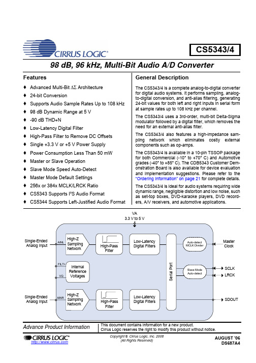
The CS5343/4 also features a high-impedance sampling network which eliminates costly external components such as op-amps.
The CS5343/4 is available in a 10-pin TSSOP package for both Commercial (-10° to +70° C) and Automotive grades (-40° to +85° C). The CDB5343 Customer Demonstration Board is also available for device evaluation and implementation suggestions. Please refer to the “Ordering Information” on page 21 for complete details.
Advance Product Information
This document contains inic reserves the right to modify this product without notice.
SPECIFIED OPERATING CONDITIONS ............................................................................................... 5 ABSOLUTE MAXIMUM RATINGS ......................................................................................................... 5 ANALOG CHARACTERISTICS - COMMERCIAL GRADE .................................................................... 6 ANALOG CHARACTERISTICS - AUTOMOTIVE GRADE ..................................................................... 7 DIGITAL FILTER CHARACTERISTICS ................................................................................................ 8 DC ELECTRICAL CHARACTERISTICS ................................................................................................ 8 DIGITAL CHARACTERISTICS .............................................................................................................. 9 SYSTEM CLOCKING AND SERIAL AUDIO INTERFACE ................................................................... 10 3. TYPICAL CONNECTION DIAGRAM ................................................................................................... 12 4. APPLICATIONS ................................................................................................................................... 13 4.1 Operation as Clock Master or Slave ............................................................................................... 13
CD4033BE,CD4026BPWRE4,CD4026BPWRG4,CD4026BNSRE4,CD4026BNSRG4, 规格书,Datasheet 资料

Data sheet acquired from Harris SemiconductorSCHS031B – Revised July 2003Copyright 2003, Texas Instruments IncorporatedThe CD4026B- and CD4033B-series types are supplied in 16-lead dual-in-line plastic packages (E suffix), 16-lead small-outline packages (NSR suffix), and 16-lead thin shrink small-outline packages (PW and PWR suffixes).PACKAGING INFORMATIONOrderable Device Status(1)PackageType PackageDrawingPins PackageQtyEco Plan(2)Lead/Ball Finish MSL Peak Temp(3)CD4026BE ACTIVE PDIP N1625Pb-Free(RoHS)CU NIPDAU N/A for Pkg TypeCD4026BEE4ACTIVE PDIP N1625Pb-Free(RoHS)CU NIPDAU N/A for Pkg TypeCD4026BNSR ACTIVE SO NS162000Green(RoHS&no Sb/Br)CU NIPDAU Level-1-260C-UNLIMCD4026BNSRE4ACTIVE SO NS162000Green(RoHS&no Sb/Br)CU NIPDAU Level-1-260C-UNLIMCD4026BNSRG4ACTIVE SO NS162000Green(RoHS&no Sb/Br)CU NIPDAU Level-1-260C-UNLIMCD4026BPW ACTIVE TSSOP PW1690Green(RoHS&no Sb/Br)CU NIPDAU Level-1-260C-UNLIMCD4026BPWE4ACTIVE TSSOP PW1690Green(RoHS&no Sb/Br)CU NIPDAU Level-1-260C-UNLIMCD4026BPWG4ACTIVE TSSOP PW1690Green(RoHS&no Sb/Br)CU NIPDAU Level-1-260C-UNLIMCD4026BPWR ACTIVE TSSOP PW162000Green(RoHS&no Sb/Br)CU NIPDAU Level-1-260C-UNLIMCD4026BPWRE4ACTIVE TSSOP PW162000Green(RoHS&no Sb/Br)CU NIPDAU Level-1-260C-UNLIMCD4026BPWRG4ACTIVE TSSOP PW162000Green(RoHS&no Sb/Br)CU NIPDAU Level-1-260C-UNLIMCD4033BE ACTIVE PDIP N1625Pb-Free(RoHS)CU NIPDAU N/A for Pkg TypeCD4033BEE4ACTIVE PDIP N1625Pb-Free(RoHS)CU NIPDAU N/A for Pkg TypeCD4033BPW ACTIVE TSSOP PW1690Green(RoHS&no Sb/Br)CU NIPDAU Level-1-260C-UNLIMCD4033BPWE4ACTIVE TSSOP PW1690Green(RoHS&no Sb/Br)CU NIPDAU Level-1-260C-UNLIMCD4033BPWG4ACTIVE TSSOP PW1690Green(RoHS&no Sb/Br)CU NIPDAU Level-1-260C-UNLIM(1)The marketing status values are defined as follows:ACTIVE:Product device recommended for new designs.LIFEBUY:TI has announced that the device will be discontinued,and a lifetime-buy period is in effect.NRND:Not recommended for new designs.Device is in production to support existing customers,but TI does not recommend using this part in a new design.PREVIEW:Device has been announced but is not in production.Samples may or may not be available.OBSOLETE:TI has discontinued the production of the device.(2)Eco Plan-The planned eco-friendly classification:Pb-Free(RoHS),Pb-Free(RoHS Exempt),or Green(RoHS&no Sb/Br)-please check /productcontent for the latest availability information and additional product content details.TBD:The Pb-Free/Green conversion plan has not been defined.Pb-Free(RoHS):TI's terms"Lead-Free"or"Pb-Free"mean semiconductor products that are compatible with the current RoHS requirements for all6substances,including the requirement that lead not exceed0.1%by weight in homogeneous materials.Where designed to be soldered at high temperatures,TI Pb-Free products are suitable for use in specified lead-free processes.Pb-Free(RoHS Exempt):This component has a RoHS exemption for either1)lead-based flip-chip solder bumps used between the die and package,or2)lead-based die adhesive used between the die and leadframe.The component is otherwise considered Pb-Free(RoHS compatible)as defined above.Green(RoHS&no Sb/Br):TI defines"Green"to mean Pb-Free(RoHS compatible),and free of Bromine(Br)and Antimony(Sb)based flame retardants(Br or Sb do not exceed0.1%by weight in homogeneous material)(3)MSL,Peak Temp.--The Moisture Sensitivity Level rating according to the JEDEC industry standard classifications,and peak solder temperature.Important Information and Disclaimer:The information provided on this page represents TI's knowledge and belief as of the date that it is provided.TI bases its knowledge and belief on information provided by third parties,and makes no representation or warranty as to the accuracy of such information.Efforts are underway to better integrate information from third parties.TI has taken and continues to take reasonable steps to provide representative and accurate information but may not have conducted destructive testing or chemical analysis on incoming materials and chemicals.TI and TI suppliers consider certain information to be proprietary,and thus CAS numbers and other limited information may not be available for release.In no event shall TI's liability arising out of such information exceed the total purchase price of the TI part(s)at issue in this document sold by TI to Customer on an annual basis.TAPE AND REEL INFORMATION*All dimensions are nominalDevicePackage Type Package Drawing Pins SPQReel Diameter (mm)Reel Width W1(mm)A0(mm)B0(mm)K0(mm)P1(mm)W (mm)Pin1Quadrant CD4026BNSR SO NS 162000330.016.48.210.5 2.512.016.0Q1CD4026BPWRTSSOPPW162000330.012.46.95.61.68.012.0Q1*All dimensions are nominalDevice Package Type Package Drawing Pins SPQ Length(mm)Width(mm)Height(mm) CD4026BNSR SO NS162000367.0367.038.0CD4026BPWR TSSOP PW162000367.0367.035.0IMPORTANT NOTICETexas Instruments Incorporated and its subsidiaries(TI)reserve the right to make corrections,enhancements,improvements and other changes to its semiconductor products and services per JESD46C and to discontinue any product or service per JESD48B.Buyers should obtain the latest relevant information before placing orders and should verify that such information is current and complete.All semiconductor products(also referred to herein as“components”)are sold subject to TI’s terms and conditions of sale supplied at the time of order acknowledgment.TI warrants performance of its components to the specifications applicable at the time of sale,in accordance with the warranty in TI’s terms and conditions of sale of semiconductor products.Testing and other quality control techniques are used to the extent TI deems necessary to support this warranty.Except where mandated by applicable law,testing of all parameters of each component is not necessarily performed.TI assumes no liability for applications assistance or the design of Buyers’products.Buyers are responsible for their products and applications using TI components.To minimize the risks associated with Buyers’products and applications,Buyers should provide adequate design and operating safeguards.TI does not warrant or represent that any license,either express or implied,is granted under any patent right,copyright,mask work right,or other intellectual property right relating to any combination,machine,or process in which TI components or services are rmation published by TI regarding third-party products or services does not constitute a license to use such products or services or a warranty or endorsement e of such information may require a license from a third party under the patents or other intellectual property of the third party,or a license from TI under the patents or other intellectual property of TI.Reproduction of significant portions of TI information in TI data books or data sheets is permissible only if reproduction is without alteration and is accompanied by all associated warranties,conditions,limitations,and notices.TI is not responsible or liable for such altered rmation of third parties may be subject to additional restrictions.Resale of TI components or services with statements different from or beyond the parameters stated by TI for that component or service voids all express and any implied warranties for the associated TI component or service and is an unfair and deceptive business practice. TI is not responsible or liable for any such statements.Buyer acknowledges and agrees that it is solely responsible for compliance with all legal,regulatory and safety-related requirements concerning its products,and any use of TI components in its applications,notwithstanding any applications-related information or support that may be provided by TI.Buyer represents and agrees that it has all the necessary expertise to create and implement safeguards which anticipate dangerous consequences of failures,monitor failures and their consequences,lessen the likelihood of failures that might cause harm and take appropriate remedial actions.Buyer will fully indemnify TI and its representatives against any damages arising out of the use of any TI components in safety-critical applications.In some cases,TI components may be promoted specifically to facilitate safety-related applications.With such components,TI’s goal is to help enable customers to design and create their own end-product solutions that meet applicable functional safety standards and requirements.Nonetheless,such components are subject to these terms.No TI components are authorized for use in FDA Class III(or similar life-critical medical equipment)unless authorized officers of the parties have executed a special agreement specifically governing such use.Only those TI components which TI has specifically designated as military grade or“enhanced plastic”are designed and intended for use in military/aerospace applications or environments.Buyer acknowledges and agrees that any military or aerospace use of TI components which have not been so designated is solely at the Buyer's risk,and that Buyer is solely responsible for compliance with all legal and regulatory requirements in connection with such use.TI has specifically designated certain components which meet ISO/TS16949requirements,mainly for automotive ponents which have not been so designated are neither designed nor intended for automotive use;and TI will not be responsible for any failure of such components to meet such requirements.Products ApplicationsAudio /audio Automotive and Transportation /automotiveAmplifiers Communications and Telecom /communicationsData Converters Computers and Peripherals /computersDLP®Products Consumer Electronics /consumer-appsDSP Energy and Lighting /energyClocks and Timers /clocks Industrial /industrialInterface Medical /medicalLogic Security /securityPower Mgmt Space,Avionics and Defense /space-avionics-defense Microcontrollers Video and Imaging /videoRFID OMAP Mobile Processors /omap TI E2E Community Wireless Connectivity /wirelessconnectivityMailing Address:Texas Instruments,Post Office Box655303,Dallas,Texas75265Copyright©2012,Texas Instruments Incorporated。
CDB5333中文资料

Preliminary Product InformationThis document contains information for a new product.Cirrus Logic reserves the right to modify this product without notice.Copyright Cirrus Logic, Inc. 2001CDB5333Evaluation Board for CS5333Featuresl Demonstrates recommended layout andgrounding arrangementsl CS8404A generates AES/EBU, S/PDIF, and EIAJ-340 compatible digital audiol Requires only an analog signal source and power supplies for a complete Analog-to-Digital-Converter systemDescriptionThe CDB5333 evaluation board is an excellent means for quickly evaluating the CS5333 24-bit, stereo A/D con-verter. Evaluation requires a digital signal analyzer, an analog signal source, and a power supply.Also included is a CS8404A digital audio interface trans-mitter which generates AES/EBU, S/PDIF, and EIAJ-340compatible audio data. The digital audio data is avail-able via RCA phono and optical connectors.ORDERING INFORMATIONCDB5333 Evaluation BoardCS5333CS8404A AES/EBU I/O FOR CLOCKS AND DATA$1$/2*Ã,1387S/PDIF S/PDIFTRANSMITTEROUTPUTJUL ‘01TABLE OF CONTENTS1. CDB5333 SYSTEM OVERVIEW (3)2. CS5333 ANALOG TO DIGITAL CONVERTER (3)3. CS8404A DIGITAL AUDIO TRANSMITTER (3)4. INPUT/OUTPUT FOR CLOCKS AND DATA (3)5. POWER SUPPLY CIRCUITRY (3)6. GROUNDING AND POWER SUPPLY DECOUPLING (3)LIST OF FIGURESFigure 1. System Block Diagram and Signal Flow (5)Figure 2. Analog Audio Input (6)Figure 3. CS5333 (7)Figure 4. Reset Circuit (7)Figure 5. Level Shifters (8)Figure 6. I/O for Clocks/Data (9)Figure 7. CS8404A Digital Audio Interface (9)Figure 8. Digital Audio Output (10)Figure 9. Power Circuit (11)Figure 10. Top Layer Silkscreen (12)Figure 11. Top Layer (13)Figure 12. Bottom Layer (14)LIST OF TABLESTable 1. System Connections (4)Table 2. CDB5333 Jumper and Switch Settings (4)Contacting Cirrus Logic SupportFor a complete listing of Direct Sales, Distributor, and Sales Representative contacts, visit the Cirrus Logic web site at: /corporate/contacts/Preliminary product information describes products which are in production, but for which full characterization data is not yet available. Advance product infor-mation describes products which are in development and subject to development changes. Cirrus Logic, Inc. has made best efforts to ensure that the information contained in this document is accurate and reliable. However, the information is subject to change without notice and is provided “AS IS” without warranty of any kind (express or implied). Customers are advised to obtain the latest version of relevant information to verify, before placing orders, that information being relied on is current and complete. All products are sold subject to the terms and conditions of sale supplied at the time of order acknowledgment, including those pertaining to warranty, patent infringement, and limitation of liability. No responsibility is assumed by Cirrus Logic, Inc. for the use of this information, including use of this information as the basis for manufacture or sale of any items, nor for infringements of patents or other rights of third parties. This document is the property of Cirrus Logic, Inc. and by furnishing this information, Cirrus Logic, Inc. grants no license, express or implied under any patents, mask work rights, copyrights, trademarks, trade secrets or other intellectual property rights of Cirrus Logic, Inc. Cirrus Logic, Inc., copyright owner of the information contained herein, gives consent for copies to be made of the information only for use within your organization with respect to Cirrus Logic integrated circuits or other parts of Cirrus Logic, Inc. The same consent is given for similar information contained on any Cirrus Logic website or disk. This consent does not extend to other copying such as copying for general distribution, advertising or promotional purposes, or for creating any work for resale. The names of products of Cirrus Logic, Inc. or other vendors and suppliers appearing in this document may be trademarks or service marks of their respective owners which may be registered in some jurisdictions. A list of Cirrus Logic, Inc. trademarks and service marks can be found at .1.CDB5333 SYSTEM OVERVIEWThe CDB5333 evaluation board is an excellent means of quickly evaluating the CS5333. The CS8404A digital audio interface transmitter pro-vides an easy interface to digital audio signal ana-lyzers including the majority of digital audio test equipment.The CDB5333 schematic has been partitioned into 8 schematics shown in Figures2 through 9. Each partitioned schematic is represented in the system diagram shown in Figure1. Notice that the system diagram also includes the interconnections be-tween the partitioned schematics.2.CS5333 ANALOG TO DIGITALCONVERTERA description of the CS5333 is included in the CS5333 datasheet.3.CS8404A DIGITAL AUDIOTRANSMITTERThe system generates and encodes standard S/P DIF data using a CS8404A Digital Audio Transmitter, Figure7. The outputs of the CS8404A are RS422 compatible differential line drivers. The CS8404A data format has been configured for I2S.A description of the CS8404A is included in the CS8404A datasheet.Note:The CS8404A can not be the clock source for the board4.INPUT/OUTPUT FOR CLOCKS ANDDATAThe evaluation board has been designed to allow interfacing to external systems via the 10-pin head-er, J6. The schematic for the clock/data input/out-put is shown in Figure6.The CDB5333 allows some flexibility as to the generation of the clocks. When in slave mode, the MCLK, SCLK, and LRCK must be provided via the header, J6. When operating the CS5333 in mas-ter mode, MCLK is generated from the on board oscillator, Y1. This oscillator is socketed to allow other frequency oscillators to be used.Note:When providing MCLK externally, the on board oscillator must be removed.5.POWER SUPPLY CIRCUITRYPower is supplied to the evaluation board by four binding posts (GND, +5V, VA, VL), see Figure 9. The +5V input supplies power to the +5V digital circuitry (+5V) and the amplifiers (VAA_+5V), while the two +1.8/+3.3V inputs supply power to the VA and VL pins of the CS5333 and to the level shifter circuits.6.GROUNDING AND POWER SUPPLYDECOUPLINGThe CS5333 requires careful attention to power supply and grounding arrangements to optimize performance. Figure3 details the power distribu-tion used on this board. The decoupling capacitors are located as close to the CS5333 as possible. Ex-tensive use of ground plane fill in the evaluation board yields large reductions in radiated noise.CONNECTOR INPUT/OUTPUT SIGNAL PRESENT+5V Input+ 5 Volt powerVA Input+ 1.8 to + 3.3 Volt power for the CS5333VL Input+ 1.8 to +3.3 Volt power for the CS5333GND Input Ground connection from power supplyLeft Audio In Input Analog input left channelRight Audio In Input Analog input right channelOptical Output Output Digital audio outputCoax Output Output Digital audio outputTable 1. System ConnectionsJUMPER /SWITCH PURPOSE POSITION FUNCTION SELECTEDJ3MCLK divide/Mode select HI*LOW Master: High Rate mode Slave: MCLK divide Master: Base Rate mode Slave: NAJ4Data format select HI*LOW Left Justified, up to 24-bit data I2S, up to 24-bit dataJ5MCLK divider for theCS8404A DIV1*DIV2DIV4MCLK goes straight to CS8404AMCLK divided by two prior to CS8404AMCLK divided by four prior to CS8404AJ7Master/Slave select forCS5333*HILOWCS5333 in Master modeCS5333 in Slave modeJ6Input/Output forclocks/data--S1Reset for the CDB5333--Notes: * denotes default factory settingsTable 2. CDB5333 Jumper and Switch SettingsD I G I T A LO U T P U T SC S 5333C S 8404AD I G I T A LA U D I OI N T E R F A C EI /O F O RC L O C K SA N D D A T AF i g u r e 1. S y s t e m B l o c k D i a g r a m a n d S i g n a l F l o wA N A L O GI N P U T SF IG 2F IG 3F IG 6F IG 7F IG 8L E V E L S H I F T E RF IG 5R E S E TC I R C U I TF IG 4F i g u r e 2. A n a l o g A u d i o I n p u tFigure 3. CS5333Figure 4. Reset CircuitFigure 5. Level ShiftersFigure 6. I/O for Clocks/DataFigure 7. CS8404A Digital Audio InterfaceFigure 8. Digital Audio OutputDS520DB311Figure 9. Power Circuit12DS520DB3F i g u r e 10. T o p L a y e r S i l k s c r e e nDS520DB313F i g u r e 11. T o p L a y e r14DS520DB3F i g u r e 12. B o t t o m L a y e r• Notes •。
CD54NP-330LB中文资料
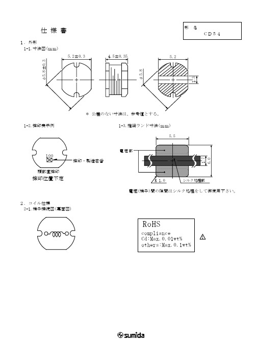
仕 様 書形 名CD541.外形1-1.寸法図(mm)* 公差のない寸法は、参考値とする。
1-2.捺印表示例 1-3.推奨ランド寸法(mm)電極(端子)間の隙間はシルク処理をして御使用下さい。
2.コイル仕様2-1.端子接続図(裏面図)5.2±0.3 4.5±0.35 5.2φ5.8φ5.8±0.31.3頭部直捺印捺印位置不定捺印・製造密番電極complianceCd:Max.0.01wt%others:Max.0.1wt%RoHS1仕 様 書形 名CD542-2.電気的特性 NO. 品 名 表示 インダクタンス[以内]※1 D.C.R.(Ω) [以下] (at 20℃)定格電流(A) ※2 S.R.F. (MHz) [参考値] スミダ コード 01 CD54NP-1ØØMC -0226 02 CD54NP-1ØØMB 100 10μH±20% 0.10 1.44 30.6 -0227 03 CD54NP-12ØMC -0228 04 CD54NP-12ØMB 120 12μH±20% 0.12 1.40 27.7 -0231 05 CD54NP-15ØMC -0232 06 CD54NP-15ØMB 150 15μH±20% 0.14 1.30 25.9 -0233 07 CD54NP-18ØMC -0234 08 CD54NP-18ØMB 180 18μH±20% 0.15 1.23 23.3 -0235 09 CD54NP-22ØMC -0236 10 CD54NP-22ØMB 220 22μH±20% 0.18 1.11 19.5 -0237 11 CD54NP-27ØMC -0238 12 CD54NP-27ØMB 270 27μH±20% 0.20 0.97 17.5 -0239 13 CD54NP-33ØLC -0240 14 CD54NP-33ØLB 330 33μH±15% 0.23 0.88 16.3 -0242 15 CD54NP-39ØLC -0243 16 CD54NP-39ØLB 390 39μH±15% 0.32 0.80 15.8 -0244 17 CD54NP-47ØLC -0245 18 CD54NP-47ØLB 470 47μH±15% 0.37 0.72 13.6 -0246 19 CD54NP-56ØKC -0247 20 CD54NP-56ØKB 560 56μH±10% 0.42 0.68 12.1 -0248 21 CD54NP-68ØKC -0249 22 CD54NP-68ØKB 680 68μH±10% 0.46 0.61 11.7 -0250 23 CD54NP-82ØKC -0251 24 CD54NP-82ØKB 820 82μH±10% 0.60 0.58 10.2 -0253 25 CD54NP-1Ø1KC -0254 26 CD54NP-1Ø1KB 101 100μH±10% 0.70 0.52 9.24 -0255 27 CD54NP-121KC -0256 28 CD54NP-121KB 121 120μH±10% 0.93 0.48 8.61 -0257 29 CD54NP-151KC -0258 30 CD54NP-151KB 151 150μH±10% 1.10 0.40 8.28 -0259 31 CD54NP-181KC -0260 32 CD54NP-181KB 181 180μH±10% 1.38 0.38 6.42 -0261 33 CD54NP-221KC -0262 34CD54NP-221KB221220μH±10%1.570.355.73-0264* 品名表示の区分(1) リール梱包の場合: CD54NP-XXXXC (2) 箱梱包の場合: CD54NP-XXXXB※1:測定周波数 L 10μH ~ 82μH ; at 2.52 MHz 100μH ~ 220μH ; at 1 kHz※2: 定格電流は直流重畳特性に於て、インダクタンスが初期値より-10%となる電流もしくは直流電流を 流した時のコイルの発熱が△t=40℃となる電流値の少ない方の値。
ON Semiconductor 1N5333B Series 数据手册

1N5333B SeriesPreferred Device5 Watt Surmetic t40 Zener Voltage RegulatorsThis is a complete series of 5 Watt Zener diodes with tight limits and better operating characteristics that reflect the superior capabilities of silicon-oxide passivated junctions. All this in an axial lead, transfer-molded plastic package that offers protection in all common environmental conditions.Features•ăZener V oltage Range - 3.3 V to 200 V•ăESD Rating of Class 3 (>16 kV) per Human Body Model•ăSurge Rating of up to 180 W @ 8.3 ms•ăMaximum Limits Guaranteed on up to Six Electrical Parameters •ăPb-Free Packages are Available*Mechanical CharacteristicsCASE:V oid free, transfer-molded, thermosetting plasticFINISH:All external surfaces are corrosion resistant and leads are readily solderableMAXIMUM LEAD TEMPERATURE FOR SOLDERING PURPOSES: 260°C, 1/16 in. from the case for 10 secondsPOLARITY:Cathode indicated by polarity bandMOUNTING POSITION:AnyMAXIMUM RATINGSRating Symbol ValueUnit Max. Steady State Power Dissipation@ T L = 75°C, Lead Length = 3/8 inDerate above 75°C P D540WmW/°COperating and StorageTemperature RangeT J, T stg-65 to +200°CStresses exceeding Maximum Ratings may damage the device. Maximum Ratings are stress ratings only. Functional operation above the Recommended Operating Conditions is not implied. Extended exposure to stresses above the Recommended Operating Conditions may affect device reliability.*For additional information on our Pb-Free strategy and soldering details, please download the ON Semiconductor Soldering and Mounting Techniques Reference Manual, SOLDERRM/D.MARKING DIAGRAMA=Assembly Location1N53xxB=Device Number(Refer to Tables on Pages 3 & 4) YY=YearWW=Work WeekG=Pb-Free PackageA1N53xxBYYWW GGDevice Package Shipping†ORDERING INFORMATIONPreferred devices are recommended choices for future use and best overall value.†For information on tape and reel specifications, including part orientation and tape sizes, please refer to our T ape and Reel Packaging Specifications Brochure, BRD8011/D.1N53xxB, G Axial Lead(Pb-Free)1000 Units/Box1N53xxBRL, G Axial Lead(Pb-Free)4000/T ape & Reel (Note: Microdot may be in either location)ELECTRICAL CHARACTERISTICS (T A = 25°C unlessotherwise noted, V F = 1.2 V Max @ I F = 1.0 A for all types)Symbol ParameterV Z Reverse Zener Voltage @ I ZTI ZT Reverse CurrentZ ZT Maximum Zener Impedance @ I ZTI ZK Reverse CurrentZ ZK Maximum Zener Impedance @ I ZKI R Reverse Leakage Current @ V RV R Breakdown VoltageI F Forward CurrentV F Forward Voltage @ I FI R Maximum Surge Current @ T A = 25°CD V Z Reverse Zener Voltage ChangeI ZM Maximum DC Zener CurrentELECTRICAL CHARACTERISTICS (T A = 25°C unless otherwise noted, V F = 1.2 V Max @ I F = 1.0 A for all types)Device†(Note 1)DeviceMarkingZener Voltage (Note 2)Zener Impedance (Note 2)LeakageCurrentI R(Note 3)D V Z(Note 4)I ZM(Note 5) V Z (Volts)@ I ZT Z ZT @ I ZT Z ZK @ I ZK I ZK I R @ V RMin Nom Max mA W W mA m A Max Volts A Volts mA1N5333B, G1N5333B 3.14 3.3 3.47380340013001200.851440 1N5334BG1N5334B 3.42 3.6 3.78350 2.55001150118.70.81320 1N5335BG1N5335B 3.71 3.9 4.103202500150117.60.541220 1N5336BG1N5336B 4.09 4.3 4.522902*********.40.491100 1N5337BG1N5337B 4.47 4.7 4.94260245015115.30.4410101N5338BG1N5338B 4.85 5.1 5.36240 1.540011114.40.39930 1N5339B, G1N5339B 5.32 5.6 5.88220140011213.40.25865 1N5340B, G1N5340B 5.70 6.0 6.30200130011312.70.19790 1N5341B, G1N5341B 5.89 6.2 6.51200120011312.40.1765 1N5342BG1N5342B 6.46 6.87.141751200110 5.211.50.157001N5343BG1N5343B7.137.57.88175 1.5200110 5.710.70.15630 1N5344B, G1N5344B7.798.28.61150 1.5200110 6.2100.2580 1N5345B, G1N5345B8.278.79.141502200110 6.69.50.2545 1N5346BG1N5346B8.659.19.56150215017.5 6.99.20.22520 1N5347B, G1N5347B9.501010.51252125157.68.60.22475 Devices listed in bold, italic are ON Semiconductor Preferred devices. Preferred devices are recommended choices for future use and best overall value.1.TOLERANCE AND TYPE NUMBER DESIGNATION: The JEDEC type numbers shown indicate a tolerance of ±5%.2.ZENER VOLTAGE (V Z) and IMPEDANCE (I ZT and I ZK): Test conditions for zener voltage and impedance are as follows: I Z is applied40 ±10 ms prior to reading. Mounting contacts are located 3/8″ to 1/2″ from the inside edge of mounting clips to the body of the diode(T A = 25°C +8°C, -2°C).3.SURGE CURRENT (I R): Surge current is specified as the maximum allowable peak, non-recurrent square-wave current with a pulse width,PW, of 8.3 ms. The data given in Figure 5 may be used to find the maximum surge current for a square wave of any pulse width between1 ms and 1000 ms by plotting the applicable points on logarithmic paper. Examples of this, using the 3.3 V and 200 V zener are shown inFigure 6. Mounting contact located as specified in Note 2 (T A = 25°C +8°C, -2°C).4.VOLTAGE REGULATION (D V Z): The conditions for voltage regulation are as follows: V Z measurements are made at 10% and then at 50%of the I Z max value listed in the electrical characteristics table. The test current time duration for each V Z measurement is 40 ±10 ms. Mounting contact located as specified in Note 2 (T A = 25°C +8°C, -2°C).5.MAXIMUM REGULATOR CURRENT (I ZM): The maximum current shown is based on the maximum voltage of a 5% type unit, therefore,it applies only to the B-suffix device. The actual I ZM for any device may not exceed the value of 5 watts divided by the actual V Z of the device.T L = 75°C at 3/8″ maximum from the device body.†The “G'' suffix indicates Pb-Free package or Pb-Free packages are available.ELECTRICAL CHARACTERISTICS (T A = 25°C unless otherwise noted, V F = 1.2 V Max @ I F = 1.0 A for all types)Device†(Note 6)DeviceMarkingZener Voltage (Note 7)Zener Impedance (Note 7)LeakageCurrentI R(Note 8)D V Z(Note 9)I ZM(Note 10) V Z (Volts)@ I ZT Z ZT @ I ZT Z ZK @ I ZK I ZK I R @ V RMin Nom Max mA W W mA m A Max Volts A Volts mA1N5348BG1N5348B10.451111.55125 2.5125158.48.00.25430 1N5349B, G1N5349B11.41212.6100 2.5125129.17.50.25395 1N5350B, G1N5350B12.351313.65100 2.5100119.97.00.25365 1N5351BG1N5351B13.31414.7100 2.5751110.6 6.70.25340 1N5352B, G1N5352B14.251515.7575 2.5751111.5 6.30.253151N5353B, G1N5353B15.21616.875 2.5751112.2 6.00.3295 1N5354B, G1N5354B16.151717.8570 2.57510.512.9 5.80.35280 1N5355B, G1N5355B17.11818.965 2.57510.513.7 5.50.4264 1N5356BG1N5356B18.051919.956537510.514.4 5.30.4250 1N5357BG1N5357B1920216537510.515.2 5.10.42371N5358B, G1N5358B20.92223.150 3.57510.516.7 4.70.45216 1N5359B, G1N5359B22.82425.250 3.510010.518.2 4.40.55198 1N5360BG1N5360B23.752526.2550411010.519 4.30.55190 1N5361B, G1N5361B25.652728.3550512010.520.6 4.10.6176 1N5362BG1N5362B26.62829.450613010.521.2 3.90.61701N5363BG1N5363B28.53031.540814010.522.8 3.70.6158 1N5364BG1N5364B31.353334.65401015010.525.1 3.50.6144 1N5365B, G1N5365B34.23637.8301116010.527.4 3.50.65132 1N5366B, G1N5366B37.053940.95301417010.529.7 3.10.65122 1N5367BG1N5367B40.854345.153********.532.7 2.80.71101N5368BG1N5368B44.654749.35252521010.535.8 2.70.8100 1N5369B, G1N5369B48.455153.55252723010.538.8 2.50.993 1N5370B, G1N5370B53.25658.8203528010.542.6 2.3 1.086 1N5371BG1N5371B576063204035010.545.5 2.2 1.279 1N5372BG1N5372B58.96265.1204240010.547.1 2.1 1.35761N5373B, G1N5373B64.66871.4204450010.551.7 2.0 1.5270 1N5374BG1N5374B71.257578.75204562010.556 1.9 1.663 1N5375BG1N5375B77.98286.1156572010.562.2 1.8 1.858 1N5377BG1N5377B86.459195.55157576010.569.2 1.6 2.252.51N5378B, G1N5378B95100105129080010.576 1.5 2.547.5 1N5380BG1N5380B11412012610170115010.591.2 1.3 2.539.5 1N5381BG1N5381B123.5130136.510190125010.598.8 1.2 2.536.61N5383B, G1N5383B142.5150157.58330150010.5114 1.1 3.031.6 1N5384BG1N5384B1521601688350165010.5122 1.1 3.029.4 1N5386BG1N5386B1711801895430175010.5137 1.0 4.026.4 1N5387BG1N5387B180.5190199.55450185010.51440.9 5.025 1N5388B, G1N5388B1902002105480185010.51520.9 5.023.6Devices listed in bold, italic are ON Semiconductor Preferred devices. Preferred devices are recommended choices for future use and best overall value.6.TOLERANCE AND TYPE NUMBER DESIGNATION: The JEDEC type numbers shown indicate a tolerance of ±5%.7.ZENER VOLTAGE (V Z) and IMPEDANCE (I ZT and I ZK): Test conditions for zener voltage and impedance are as follows: I Z is applied40 ±10 ms prior to reading. Mounting contacts are located 3/8″ to 1/2″ from the inside edge of mounting clips to the body of the diode(T A = 25°C +8°C, -2°C).8.SURGE CURRENT (I R): Surge current is specified as the maximum allowable peak, non-recurrent square-wave current with a pulse width,PW, of 8.3 ms. The data given in Figure 5 may be used to find the maximum surge current for a square wave of any pulse width between1 ms and 1000 ms by plotting the applicable points on logarithmic paper. Examples of this, using the 3.3 V and 200 V zener are shown inFigure 6. Mounting contact located as specified in Note 7 (T A = 25°C +8°C, -2°C).9.VOLTAGE REGULATION (D V Z): The conditions for voltage regulation are as follows: V Z measurements are made at 10% and then at 50%of the I Z max value listed in the electrical characteristics table. The test current time duration for each V Z measurement is 40 ±10 ms. Mounting contact located as specified in Note 7 (T A = 25°C +8°C, -2°C).10.MAXIMUM REGULATOR CURRENT (I ZM): The maximum current shown is based on the maximum voltage of a 5% type unit, therefore,it applies only to the B-suffix device. The actual I ZM for any device may not exceed the value of 5 watts divided by the actual V Z of the device.T L = 75°C at 3/8″ maximum from the device body.†The “G'' suffix indicates Pb-Free package or Pb-Free packages are available.Figure 1. Typical Thermal ResistanceL, LEAD LENGTH TO HEATSINK (INCH)J L , J U N C T I O N ‐T O ‐L E A D T H E R M A L R E S I S T A N C E (θ°C /W )TEMPERATURE COEFFICIENTSFigure 2. Temperature Coefficient‐Range for Units 3 to 10 VoltsFigure 3. Temperature Coefficient‐Range for Units 10 to 220 VoltsV Z , ZENER VOLTAGE @ I ZT (VOLTS)1086420-2300200100503020105V Z , ZENER VOLTAGE @ I ZT (VOLTS)θV Z , T E M P E R A T U R E C O E F F I C I E N T (m V /°C ) @ I Z TθV Z , T E M P E R A T U R E C O E F F I C I E N T (m V /°C ) @ I Z TFigure 4. Typical Thermal ResponseL, Lead Length = 3/8 InchFigure 5. Maximum Non‐Repetitive Surge Currentversus Nominal Zener Voltage(See Note 3)θJ L (t , D ), T R A N S I E N T T H E R M A L R E S I S T A N C E J U N C T I O N ‐T O ‐L E A D (°C /W )t, TIME (SECONDS)I r , P E A K S U R G E C U R R E N T (A M P S )4020104210.10.20.4NOMINAL V Z (V)3020100.10.20.512510001001010.1I Z , Z E N E R C U R R E N T (m A )PW, PULSE WIDTH (ms)V Z , ZENER VOLTAGE (VOLTS)Figure 6. Peak Surge Current versus Pulse Width(See Note 3)Figure 7. Zener Voltage versus Zener CurrentV Z Ă=Ă3.3 thru 10 Volts I r , P E A K S U R G E C U R R E N T (A M P S )I Z , Z E N E R C U R R E N T (m A )V Z , ZENER VOLTAGE (VOLTS)10001001010.1Figure 8. Zener Voltage versus Zener CurrentV Z = 11 thru 75 Volts1001010.180100120140160180200220V Z , ZENER VOLTAGE (VOLTS)I Z , Z E N E R C U R R E N T (m A )Figure 9. Zener Voltage versus Zener CurrentV Z = 82 thru 200 VoltsAPPLICATION NOTESince the actual voltage available from a given Zener diode is temperature dependent, it is necessary to determine junction temperature under any set of operating conditions in order to calculate its value. The following procedure is recommended:Lead Temperature, T L , should be determined from:T L = q LA P D + T Aq LA is the lead‐to‐ambient thermal resistance and P D is the power dissipation.Junction Temperature, T J , may be found from:T J = T L + D T JLD T JL is the increase in junction temperature above the lead temperature and may be found from Figure 4 for a train of power pulses or from Figure 1 for dc power.D T JL = q JL P DFor worst‐case design, using expected limits of I Z , limits of P D and the extremes of T J (D T J ) may be estimated.Changes in voltage, V Z , can then be found from:D V = q VZ D T Jq VZ , the Zener voltage temperature coefficient, is found from Figures 2 and 3.Under high power‐pulse operation, the Zener voltage will vary with time and may also be affected significantly by the zener resistance. For best regulation, keep current excursions as low as possible.Data of Figure 4 should not be used to compute surge capability. Surge limitations are given in Figure 5. They are lower than would be expected by considering only junction temperature, as current crowding effects cause temperatures to be extremely high in small spots resulting in device degradation should the limits of Figure 5 be exceeded.PACKAGE DIMENSIONSSURMETIC 40, AXIAL LEADCASE 017AA-01ISSUE ODIM MIN MAX MIN MAX MILLIMETERSINCHES A 0.3300.3508.388.89B 0.1300.145 3.30 3.68D 0.0370.0430.94 1.09F ---0.050--- 1.27K1.000 1.25025.4031.75NOTES:1.CONTROLLING DIMENSION: INCH2.LEAD DIAMETER AND FINISH NOT CONTROLLED WITHIN DIMENSION F.3.CATHODE BAND INDICATES POLARITYON Semiconductor and are registered trademarks of Semiconductor Components Industries, LLC (SCILLC). SCILLC reserves the right to make changes without further noticeto any products herein. SCILLC makes no warranty, representation or guarantee regarding the suitability of its products for any particular purpose, nor does SCILLC assume any liability arising out of the application or use of any product or circuit, and specifically disclaims any and all liability, including without limitation special, consequential or incidental damages.“Typical” parameters which may be provided in SCILLC data sheets and/or specifications can and do vary in different applications and actual performance may vary over time. All operating parameters, including “Typicals” must be validated for each customer application by customer's technical experts. SCILLC does not convey any license under its patent rights nor the rights of others. SCILLC products are not designed, intended, or authorized for use as components in systems intended for surgical implant into the body, or other applications intended to support or sustain life, or for any other application in which the failure of the SCILLC product could create a situation where personal injury or death may occur. Should Buyer purchase or use SCILLC products for any such unintended or unauthorized application, Buyer shall indemnify and hold SCILLC and its officers, employees, subsidiaries, affiliates,and distributors harmless against all claims, costs, damages, and expenses, and reasonable attorney fees arising out of, directly or indirectly, any claim of personal injury or death associated with such unintended or unauthorized use, even if such claim alleges that SCILLC was negligent regarding the design or manufacture of the part. SCILLC is an Equal Opportunity/Affirmative Action Employer. This literature is subject to all applicable copyright laws and is not for resale in any manner.SURMETIC is a trademark of Semiconductor Components Industries, LLC (SCILLC).PUBLICATION ORDERING INFORMATION。
Z5SMB5333B中文资料

V Z(V)
Min. 3.1 3.4 3.7 4.1 4.5 4.8 5.3 5.7 5.9 6.5 7.1 7.8 8.3 8.7 9.5 10.5 11.4 12.4 13.3 14.3 15.2 16.2 17.1 18.1 19.0 20.9 22.8 23.8 25.7 26.6 28.5 31.4 Max. 3.5 3.8 4.1 4.5 4.9 5.4 5.9 6.3 6.5 7.1 7.9 8.6 9.1 9.6 10.5 11.6 12.6 13.7 14.7 15.8 16.8 17.9 18.9 20.0 21.0 23.1 25.2 26.3 28.4 29.4 31.5 34.7
3.0 2.5 2.0 2.0 2.0 1.5 1.0 1.0 1.0 1.0 1.0 1.0 1.0 2.0 2.0 2.0 2.5 2.5 2.5 2.5 2.5 2.5 2.5 3.0 3.0 3.5 3.5 4.0 5.0 6.0 8.0 10
ZZK @ Izk
400 500 500 500 450 400 400 300 200 200 200 200 200 150 125 125 125 100 75 75 75 75 75 75 75 75 100 110 120 130 140 150
VR(V) IZM(mA)
1.0 1.0 1.0 1.0 1.0 1.0 2.0 3.0 4.0 4.9 5.4 5.9 6.3 6.6 7.2 8.0 8.6 9.4 10.1 10.8 11.5 12.2 13.0 13.7 14.4 15.8 17.3 18.0 19.4 20.1 21.6 23.8 1440 1320 1220 1100 1010 930 856 790 765 700 630 580 545 520 475 430 395 365 340 315 295 280 265 250 237 216 198 190 176 170 158 144
SMBG5334B中文资料
Features
• Low profile package for surface mounting (flat handling surface for accurate placement)
• Zener Voltage 3.3V to 200V • High Surge Current Capability • For available tolerances – see note 1 • Available on Tape and Reel (see EIA std RS-481)
400
14.4
0.39
400
13.4
0.25
300
12.7
0.19
200
12.4
0.10
200
11.5
0.15
200
10.7
0.15
200
10
0.20
200
9.5
0.20
150
9.2
0.22
125
8.6
0.22
125
8.0
0.25
125
7.5
0.257
0.25
75
6.3
0.25
1.1
3.00
1660
1.1
3.00
1750
1.0
3.00
1750
1.0
4.00
1850
0.9
5.00
1850
0.9
5.00
元器件交易网
SMB(G or J)5333B thru SMB(G or J)5333B
Note 1
Devices listed have a ± 5% tolerance on nominal V Z. The suffix A denotes a ± 20% tolerance, suffix C denotes ± 2%, and suffix D denotes ± 1%.
CZ5338B中文资料

MAXIMUM REVERSE CURRENT IR @ VR µA
300 150 50 10 10 10 10 10 10 100 100 100 100 7.5 5.0 5.0 2.0 1.0 1.0 1.0 1.0 0.5 0.5 0.5 0.5 0.5 0.5 0.5
MAX SURGE CURRENT (NOTE 1)
V
20.6 21.2 22.8 25.1 27.4 29.7 32.7 35.8 38.8 42.6 45.5 47.1 51.7 56.0 62.2 66.0 69.2 76.0 83.6 91.2 98.8 106 114 122 129 137 144 152
Note 1. Surge Current (ir) - Maximum allowable peak, non recurrent square wave current (PW=8.3ms). Note 2. Voltage Regulation (ΔVZ) - VZ Measurements are made at 10% and then at 50% of the IZ max value listed in the electrical characteristics table. The test current time duration for each VZ measurement is 380us (TA=25oC)
TM
Semiconductor Corp.
TEST CURRENT
5.0W SILICON ZENER DIODE 3.3 VOLTS THRU 200 VOLTS 5% TOLERANCE
ELECTRICAL CHARACTERISTICS: (TA=25°C) VF=1.2V MAX @ IF=1.0A FOR ALL TYPES.
1N5338B中文资料
(V)
0.85 0.80 0.54 0.49 0.44 0.39 0.25 0.19 0.10 0.15 0.15 0.2 0.2 0.22 0.22 0.25 0.25 0.25 0.25 0.25 0.3 0.35 0.4 0.4 0.4 0.45 0.55 0.55 0.6 0.6 0.6 0.6 0.65 0.65 0.7 0.8 0.9 1 1.2 1.35 1.5 1.6 1.8 2 2.2 2.5 2.5 2.5 2.5 2.5 3 3 3 4 5 5
(mA)
1 1 1 1 1 1 1 1 1 1 1 1 1 1 1 1 1 1 1 1 1 1 1 1 1 1 1 1 1 1 1 1 1 1 1 1 1 1 1 1 1 1 1 1 1 1 1 1 1 1 1 1 1 1 1 1
(µA)
100 75 25 15 10 5 5 5 5 10 10 10.0 10.0 7.5 5.0 5.0 2.0 1.0 1.0 1.0 1.0 0.5 0.5 0.5 0.5 0.5 0.5 0.5 0.5 0.5 0.5 0.5 0.5 0.5 0.5 0.5 0.5 0.5 0.5 0.5 0.5 0.5 0.5 0.5 0.5 0.5 0.5 0.5 0.5 0.5 0.5 0.5 0.5 0.5 0.5 0.5
(A)
20 18.7 17.6 16.4 15.3 14.4 13.3 12.7 12.4 11.5 10.7 10 9.5 9.2 8.6 8.0 7.5 7.0 6.7 6.3 6.0 5.8 5.5 5.3 5.1 4.7 4.4 4.3 4.1 3.9 3.7 3.5 3.3 3.1 2.8 2.7 2.5 2.3 2.2 2.1 2.0 1.9 1.8 1.7 1.6 1.5 1.4 1.3 1.2 1.2 1.1 1.1 1.0 1.0 0.9 0.9
MIC5333中文资料

Features
• 2.3V to 5.5V input voltage range • 300mA output current per LDO • Very low quiescent current: 25µA per LDO • POR output with programmable delay for each LDO • High PSRR – >65dB on each LDO • Stable with 1µF ceramic output capacitors • Tiny 10-pin 2.5mm x 2.5mm Thin MLF® package • Ultra-low dropout voltage – 120mV @ 300mA • Low output voltage noise – 50µVrms • Thermal shutdown protection • Current limit protection
2.5mm x 2.5mm Thin MLF-10 (θJA) ...................75°C/W
8
9 10
Pin Name VIN GND
POR2 POR1 EN2 EN1 CSET1
CSET2
VOUT2 VOUT1
Pin Function
Supply Input.
Ground.
Power-On Reset Output (Regulator 2): Open-drain output. Active low indicates an output under-voltage condition on regulator 2 when the device is enabled.
BD533资料
BD533/5/7BD534/6/8COMPLEMENTARY SILICON POWER TRANSISTORSsBD534,BD535,BD536,BD537AND BD538ARE SGS-THOMSON PREFERRED SALESTYPESDESCRIPTIONThe BD533,BD535,and BD537are silicon epitaxial-base NPN power transistors in Jedec TO-220plastic package,intented for use in medium power linear and switching applications.The complementary PNP types are BD534,BD536,and BD538respectively.INTERNAL SCHEMATIC DIAGRAMJune 1997ABSOLUTE MAXIMUM RATINGSSymbolParameterValueUnitNPN BD533BD535BD537PNPBD534BD536BD538V CBO Collector-Base Voltage (I E =0)456080V V CES Collector-Emitter Voltage (V BE =0)456080V V CEO Collector-Emitter Voltage (I B =0)456080V V EBO Emitter-Base Voltage (I C =0)5V I C,I E Collector and Emitter Current 8A I B Base Current1A P t ot Total Dissipation at T c ≤ 25 oC 50WT stg Storage Temperature-65to 150o C T jMax.Operating Junction Temperature150oCFor PNP types voltage and current values are negative.123TO-2201/4THERMAL DATAR t hj-ca se R t hj-amb Thermal Resistance Junction-case MaxThermal Resistance Junction-ambient Max2.570o C/Wo C/WELECTRICAL CHARACTERISTICS(T case=25o C unless otherwise specified)Symbol Parameter Test Conditions Min.Typ.Max.UnitI CBO Collector Cut-offCurrent(I E=0)for BD533/534V CB=45Vfor BD535/536V CB=60Vfor BD537/538V CB=80V100100100µAµAµAI CES Collector Cut-offCurrent(V BE=0)for BD533/534V CE=45Vfor BD535/536V CE=60Vfor BD537/538V CE=80V100100100µAµAµAI EBO Emitter Cut-off Current(I C=0)V EB=5V1mAV CEO(sus)∗Collector-EmitterSustaining Voltage(I B=0)I C=100mA for BD533/534for BD535/536for BD537/538456080VVVV CE(sat)∗Collector-EmitterSaturation Voltage I C=2A I B=0.2AI C=6A I B=0.6A0.80.8VVV BE∗Base-Emitter Voltage I C=2A V CE=2V 1.5V h FE∗DC Current Gain I C=10mA V CE=5Vfor BD533/534for BD535/536for BD537/538 I C=500mA V CE=2VI C=2A V CE=2Vfor BD533/534for BD535/536for BD537/53820 20 15 40 25 25 15f T Transition frequency I C=500mA V CE=1V312MHz ∗ Pulsed:Pulse duration=300µs,duty cycle1.5%For PNP types voltage and current values are negative.Safe Operating AreasBD533/BD534/BD535/BD536/BD537/BD5382/4DIM.mminch MIN.TYP.MAX.MIN.TYP.MAX.A 4.40 4.600.1730.181C 1.23 1.320.0480.051D 2.402.720.0940.107D1 1.270.050E 0.490.700.0190.027F 0.610.880.0240.034F1 1.14 1.700.0440.067F2 1.14 1.700.0440.067G 4.95 5.150.1940.203G1 2.4 2.70.0940.106H210.010.400.3930.409L216.40.645L413.014.00.5110.551L5 2.65 2.950.1040.116L615.2515.750.6000.620L7 6.2 6.60.2440.260L9 3.5 3.930.1370.154DIA.3.75 3.850.1470.151P011CTO-220MECHANICAL DATABD533/BD534/BD535/BD536/BD537/BD5383/4BD533/BD534/BD535/BD536/BD537/BD538Information furnished is believed to be accurate and reliable.However,SGS-THOMSON Microelectronics assumes no responsability for the consequences of use of such information nor for any infringementof patents or other rights of third parties which may results from its use.No license is granted by implication or otherwise under any patent or patent rights of SGS-THOMSON Microelectronics.Specifications mentioned in this publication are subject to change without notice.This publicationsupersedes and replaces all information previously supplied.SGS-THOMSON Microelectronics products are notauthorized for use as critical components in life support devices or systems without express written approval of SGS-THOMSON Microelectonics.©1997SGS-THOMSON Microelectronics-Printed in Italy-All Rights ReservedSGS-THOMSON Microelectronics GROUP OF COMPANIESAustralia-Brazil-Canada-China-France-Germany-Hong Kong-Italy-Japan-Korea-Malaysia-Malta-Morocco-The Netherlands-Singapore-Spain-Sweden-Switzerland-Taiwan-Thailand-United Kingdom-U.S.A...4/4。
- 1、下载文档前请自行甄别文档内容的完整性,平台不提供额外的编辑、内容补充、找答案等附加服务。
- 2、"仅部分预览"的文档,不可在线预览部分如存在完整性等问题,可反馈申请退款(可完整预览的文档不适用该条件!)。
- 3、如文档侵犯您的权益,请联系客服反馈,我们会尽快为您处理(人工客服工作时间:9:00-18:30)。
1000
500 400 300 200
100
50 40 30 20
10
5 4 3 2
1
2
5
10 20
50 100
OPERATING CURRENT lZT (mA)
FIGURE 3
200 500 1000
ZENER IMPEDANCE VS. OPERATING CURRENT
NOTE 1 Zener voltage range equals nominal voltage + 5% for “B” Suffix. “A” Suffix denotes + 10%. No Suffix denotes + 20%. "C" suffix = + 2% and "D" suffix = + 1%.
500 620 720 760 760
800 1000
64 MILS 58 MILS
BACKSIDE IS CATHODE
FIGURE 1
DESIGN DATA
METALLIZATION: Top: (Anode)....................Al Back: (Cathode).......... ...Au
CD5333B thru CD5379B 100
50
20
MAXIMUM RATINGS
10
Operating Temperature: -65°C to +200°C
Storage Temperature: -65°C to +200°C Forward Voltage @ 1.0Amp = 1.5 Volts maximum
NOTE 2 Zener impedance is derived by superimposing on lZT and lZK, A 60 Hz rms a.c. current equal to 10% of lZT and lZK. NOTE 3 Zener voltage is read using a pulse measurement, 10 milliseconds maximum.
58 MILS 64 MILS
元器件交易网
• ZENER DIODE CHIPS • ALL JUNCTIONS COMPLETELY PROTECTED WITH SILICON DIOXIDE • ELECTRICALLY EQUIVALENT TO 1N5333B THRU 1N5379B • 5 WATT CAPABILITY WITH PROPER HEAT SINKING • COMPATIBLE WITH ALL WIRE BONDING AND DIE ATTACH TECHNIQUES,
5
2
ZENER IMPEDANCE ZZT (OHMS)
1
.5
.2
ZENER IMPEDANCE ZZT (OHMS)
1
2
5
10
20
50 100 200
OPERATING CURRENT lZT (mA)
FIGURE 2
500 1000
ZENER IMPEDANCE VS. OPERATING CURRENT
1.0
1.0
1.0
2.0
1.0
3.0
1.0
3.0
10
5.2
10
5.7
10
6.2
10
6.6
7.5
6.9
5.0
7.6
5.0
8.4
2.0
9.1
1.0
9.9
1.0
10.6
1.0
11.5
1.0
12.2
0.5
12.9
0.5
13.7
0.5
14.4
0.5
15.2
0.5
16.7
0.5
18.2
0.5
19
0.5
20.6
0.5
40 40 30 30 30
25 25 20 20 20
20 20 15 15 15
12 12
MAXIMUM ZENER
IMPEDANCE ZZT
(Note 2)
OHMS
3.0 2.5 2.0 2.0 2.0
1.5 1.0 1.0 1.0 1.0
1.5 1.5 2.0 2.0 2.0
2.5 2.5 2.5 2.5 2.5
(Note 2)
OHMS
400 500 500 500 450
400 400 300 200 200
200 200 200 150 125
125 125 100
75 75
75 75 75 75 75
75 100 110 120 130
140 150 160 170 190
210 230 280 350 400
WITH THE EXCEPTION OF SOLDER REFLOW
CD5333B thru
CD5379B
ELECTRICAL CHARACTERISTICS @ 25°C, unless otherwise specified
TYPE NUMBER
CD5333B CD5334B CD5335B CD5336B CD5337B
CD5338B CD5339B CD5340B CD5341B CD5342B
CD5343B CD5344B CD5345B CD5346B CD5347B
CD5348B CD5349B CD5350B CD5351B CD5352B
CD5353B CD5354B CD5355B CD5356B CD5357B
22 COREY STREET, MELROSE, MASSACHUSETTS 02176
PHONE (781) 665-1071
FAX (781) 665-7379
WEBSITE: E-mail: mail@
元器件交易网
2.5 2.5 2.5 3.0 3.0
3.5 3.5 4.0 5.0 6.0
8.0 10 11 14 20
25 27 35 40 42
44 45 65 75 75
90 125
MAXIMUM REVERSE
CURRENT
lR @ VR
µA
VOLTS
300
1.0
150
1.0
50
1.0
10
1.0
5.0
1.0
47 51 56 60 62
68 75 82 87 91
100 110
TEST CURRENT
lZT mA
380 350 320 290 260
240 220 200 200 175
175 150 150 150 125
125 100 100 100
75
75 70 65 65 65
50 50 50 50 50
21.2
0.5
22.8
0.5
25.1
0.5
27.4
0.5
29.7
0.5Βιβλιοθήκη 32.70.535.8
0.5
38.8
0.5
42.6
0.5
45.5
0.5
47.1
0L5
51.7
0.5
56
0.5
62.2
0.5
66
0.5
69.2
0.5
76
0.5
83.6
MAXIMUM ZENER KNEE IMPEDANCE ZZK @ 1.0 mA
CD5378B CD5379B
NOMINAL ZENER
VOLTAGE VZ
(Note 1)
V
3.3 3.6 3.9 4.3 4.7
5.1 5.6 6.0 6.2 6.8
7.5 8.2 8.7 9.1 10
11 12 13 14 15
16 17 18 19 20
22 24 25 27 28
30 33 36 39 43
CD5358B CD5359B CD5360B CD5361B CD5362B
CD5363B CD5364B CD5365B CD5366B CD5367B
CD5368B CD5369B CD5370B CD5371B CD5372B
CD5373B CD5374B CD5375B CD5376B CD5377B