SA261中文资料
AM26LS31中文资料

50% Duty Cycle tTLH, tTHL
MOTOROLA ANALOG IC DEVICE DATA
3
元器件交易网
AM26LS31
OUTLINE DIMENSIONS
D SUFFIX PLASTIC PACKAGE CASE 751B–05 (SO–16) ISSUE J
2
MOTOROLA ANALOG IC DEVICE DATA
元器件交易网
AM26LS31
Figure 1. Three–State Enable Test Circuit and Waveforms
To Scope (Input) 3.0 V or Gnd Input Inv Output To Scope Output
≈ 1.5 V tPLZ(E) Output 0.5 V ≈ 1.5 V
Figure 2. Propagation Delay Times Input to Output Waveforms and Test Circuit
Scope (Output) Scope (Input) Inv Output 200 5.0 V
Outputs
ORDERING INFORMATION
Device AM26LS31PC MC26LS31D*
© Motorola, Inc. 1995
Operating Temperature Range TA = 0 to +70°C
Package Plastic DIP SO–16
L = Low Logic State H = High Logic Stan–Inv Output 3.0 V Enable CL = 30 pF 75
ASE261.01.Intro

System Element
AWACS Rivet Joint
Recce
Joint Stars
MCE Mission Control Element (MCE)
Target Set
Launch and Recovery Element (LRE)
Lockheed Martin Aeronautics Company
Communications Network
c 2003 LM Corporation Course Introduction 1-6
Design of UAV Systems
Air Vehicle Element
The Airplane(s)
c 2003 LM Corporation
Course Introduction
c 2003 LM Corporation Course Introduction 1-2
Design of UAV Systems
But first what is a UAV?
My definition - A reusable unmanned (or uninhabited if you prefer) air vehicle • Includes target drones but excludes cruise missiles - Even if the cruise missile has a data link - Even if the technology is similar (which it is)
c 2003 LM Corporation Course Introduction
Next subject
1-11
贝利摩纽斯型号B261的技术数据录表说明书
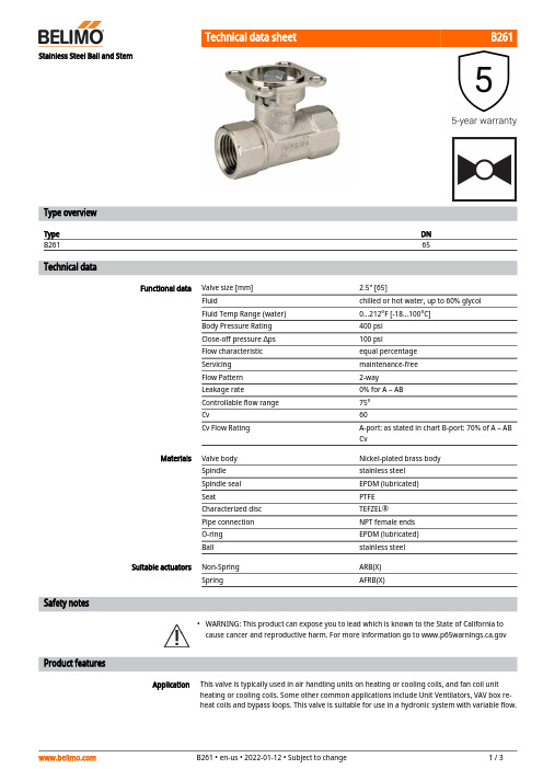
B261•ApplicationStainless Steel Ball and StemType overviewType DN B26165Technical dataFunctional dataValve size [mm] 2.5" [65]Fluidchilled or hot water, up to 60% glycol Fluid Temp Range (water)0...212°F [-18...100°C]Body Pressure Rating 400 psi Close-off pressure ∆ps 100 psiFlow characteristic equal percentage Servicing maintenance-free Flow Pattern 2-way Leakage rate0% for A – AB Controllable flow range 75°Cv60Cv Flow RatingA-port: as stated in chart B-port: 70% of A – AB CvMaterials Valve body Nickel-plated brass body Spindle stainless steel Spindle seal EPDM (lubricated)SeatPTFE Characterized disc TEFZEL®Pipe connection NPT female ends O-ring EPDM (lubricated)Ballstainless steel Suitable actuators Non-Spring ARB(X)SpringAFRB(X)Safety notesWARNING: This product can expose you to lead which is known to the State of California to cause cancer and reproductive harm. For more information go to Product featuresThis valve is typically used in air handling units on heating or cooling coils, and fan coil unit heating or cooling coils. Some other common applications include Unit Ventilators, VAV box re-heat coils and bypass loops. This valve is suitable for use in a hydronic system with variable flow.B261 Flow/Mounting detailsTwo-way valves should be installed with thedisc upstream.DimensionsType DNB26165ARB, ARXA B C D E F H110.1" [257] 5.6" [141]8.0" [203] 6.0" [152] 2.8" [71] 2.8" [71] 1.9" [48]AFRB, AFRXA B C D E F11.5" [293] 5.6" [141]8.6" [219] 6.6" [168] 2.0" [51] 2.0" [51]ARQB, ARQXA B C D E F H1H29.9" [251] 4.2" [107]8.1" [206] 6.1" [155] 2.3" [58] 2.3" [58]0.8" [20]0.6" [15]B261AFRB N4, AFRX N4A B D E F11.4" [289] 5.6" [141]8.0" [203] 2.4" [62] 2.4" [62]ARB N4, ARX N4, NRB N4, NRX N4A B D E F11.4" [289] 5.6" [141]8.0" [203] 3.1" [80] 3.1" [80]ARX24-MFT-TModulating, Non-Spring Return, 24 V, Multi-Function Technology®Technical dataElectrical dataNominal voltageAC/DC 24 V Nominal voltage frequency 50/60 Hz Power consumption in operation 3.5 W Power consumption in rest position 1.3 WTransformer sizing 6 VA (class 2 power source)Electrical Connection Terminal blocksOverload Protectionelectronic throughout 0...95° rotation Functional dataOperating range Y 2...10 VOperating range Y note 4...20 mA w/ ZG-R01 (500 Ω, 1/4 W resistor)Input Impedance100 kΩ for 2...10 V (0.1 mA), 500 Ω for 4...20 mA, 1500 Ω for PWM, On/Off and Floating point Operating range Y variable Start point 0.5...30 V End point 2.5...32 VOptions positioning signal variable (VDC, on/off, floating point)Position feedback U 2...10 V Position feedback U note Max. 0.5 mA Position feedback U variable VDC variableDirection of motion motor selectable with switch 0/1Manual override external push button Angle of rotation 90°Angle of rotation note adjustable with mechanical stop Running Time (Motor)150 s / 90°Running time motor variable 90...350 s Noise level, motor 45 dB(A)Position indicationMechanically, pluggable Safety dataDegree of protection IEC/EN IP54Degree of protection NEMA/UL NEMA 2Enclosure UL Enclosure Type 2Agency ListingcULus acc. to UL60730-1A/-2-14, CAN/CSA E60730-1:02, CE acc. to 2014/30/EU and2014/35/EU; Listed to UL 2043 - suitable for use in air plenums per Section 300.22(c) of the NEC and Section 602.2 of the IMC Quality Standard ISO 9001Ambient temperature -22...122°F [-30...50°C]Storage temperature -40...176°F [-40...80°C]Ambient humidity Max. 95% RH, non-condensing Servicingmaintenance-freeMaterialsHousing materialGalvanized steel and plastic housingARX24-MFT-TFootnotes†Rated Impulse Voltage 800 V, Type action 1, Control Pollution Degree 3.AccessoriesGatewaysDescriptionType Gateway MP to BACnet MS/TP UK24BAC Gateway MP to Modbus RTU UK24MOD Gateway MP to LonWorksUK24LON Electrical accessoriesDescriptionType Battery backup system, for non-spring return models NSV24 US Battery, 12 V, 1.2 Ah (two required)NSV-BAT Service Tool, with ZIP-USB function, for programmable andcommunicative Belimo actuators, VAV controller and HVAC performance devicesZTH USService toolsDescriptionTypeConnection cable 10 ft [3 m], A: RJ11 6/4 ZTH EU, B: 3-pin Weidmüller and supply connectionZK4-GEN Service Tool, with ZIP-USB function, for programmable and communicative Belimo actuators, VAV controller and HVAC performance devicesZTH USElectrical installationINSTALLATION NOTESActuators with appliance cables are numbered.Provide overload protection and disconnect as required.Actuators may be connected in parallel. Power consumption and input impedance must beobserved.Actuators may also be powered by DC 24 V.Only connect common to negative (-) leg of control circuits.A 500 Ω resistor (ZG-R01) converts the 4...20 mA control signal to 2...10 V.For triac sink the Common connection from the actuator must be connected to the Hotconnection of the controller. Position feedback cannot be used with a triac sink controller; theactuator internal common reference is not compatible.Actuators may be connected in parallel if not mechanically linked. Power consumption andinput impedance must be observed.IN4004 or IN4007 diode. (IN4007 supplied, Belimo part number 40155).Actuators are provided with a numbered screw terminal strip instead of a cable.Meets cULus requirements without the need of an electrical ground connection.Warning! Live electrical components!During installation, testing, servicing and troubleshooting of this product, it may be necessary to work with live electrical components. Have a qualified licensed electrician or other individual who has been properly trained in handling live electrical components perform these tasks. Failure to follow all electrical safety precautions when exposed to live electrical components could result in death or serious injury.Wiring diagramsOn/Off AC 24 V TransformerARX24-MFT-T Floating Point AC 24 V Transformer (AC Only)V/mA Control AC 24 V TransformerOverride Control。
26LS31中文资料
元器件交易网IMPORTANT NOTICETexas Instruments and its subsidiaries (TI) reserve the right to make changes to their products or to discontinueany product or service without notice, and advise customers to obtain the latest version of relevant informationto verify, before placing orders, that information being relied on is current and complete. All products are soldsubject to the terms and conditions of sale supplied at the time of order acknowledgement, including thosepertaining to warranty, patent infringement, and limitation of liability.TI warrants performance of its semiconductor products to the specifications applicable at the time of sale inaccordance with TI’s standard warranty. Testing and other quality control techniques are utilized to the extentTI deems necessary to support this warranty. Specific testing of all parameters of each device is not necessarilyperformed, except those mandated by government requirements.CERTAIN APPLICATIONS USING SEMICONDUCTOR PRODUCTS MAY INVOLVE POTENTIAL RISKS OFDEATH, PERSONAL INJURY, OR SEVERE PROPERTY OR ENVIRONMENTAL DAMAGE (“CRITICALAPPLICATIONS”). TI SEMICONDUCTOR PRODUCTS ARE NOT DESIGNED, AUTHORIZED, ORWARRANTED TO BE SUITABLE FOR USE IN LIFE-SUPPORT DEVICES OR SYSTEMS OR OTHERCRITICAL APPLICATIONS. INCLUSION OF TI PRODUCTS IN SUCH APPLICATIONS IS UNDERSTOOD TOBE FULLY AT THE CUSTOMER’S RISK.In order to minimize risks associated with the customer’s applications, adequate design and operatingsafeguards must be provided by the customer to minimize inherent or procedural hazards.TI assumes no liability for applications assistance or customer product design. TI does not warrant or representthat any license, either express or implied, is granted under any patent right, copyright, mask work right, or otherintellectual property right of TI covering or relating to any combination, machine, or process in which suchsemiconductor products or services might be or are used. TI’s publication of information regarding any thirdparty’s products or services does not constitute TI’s approval, warranty or endorsement thereof.Copyright © 1998, Texas Instruments Incorporated。
高速光耦6N137HCPL2601,HCPL2611,HCPL2630,HCPL2631中文资料

高速光耦6N137HCPL2601,HCPL2611,HCPL2630,HCPL2631中文资料高速光耦6N137/HCPL2601,HCPL2611,HCPL2630,HCPL2631中文资料常用高速光电耦合器型号:单通道: 6N137 , HCPL2601 , HCPL2611双通道: HCPL2630 , HCPL2631高速10MBit / s的逻辑门光电作用:6N137/HCPL2601,HCPL2611,HCPL2630,HCPL2631是高速光电耦合器内部结构框图6N137/HCPL2601,HCPL2611,HCPL2630,HCPL2631的内部结构原理如下图所示,信号从脚2和脚3输入,发光二极管发光,经片内光通道传到光敏二极管,反向偏置的光敏管光照后导通,经电流-电压转换后送到与门的一个输入端,与门的另一个输入为使能端,当使能端为高时与门输出高电平,经输出三极管反向后光电隔离器输出低电平。
当输入信号电流小于触发阈值或使能端为低时,输出高电平,但这个逻辑高是集电极开路的,可针对接收电路加上拉电阻或电压调整电路。
引脚图原理如上图所示,若以脚2为输入,脚3接地,则真值表如附表所列,这相当于非门的传输,若希望在传输过程中不改变逻辑状态,则从脚3输入,脚2接高电平。
6N137/HCPL2601,HCPL2611,HCPL2630,HCPL2631真值表真值表功能(正逻辑)高速光耦6N137/HCPL2601,HCPL2611,HCPL2630,HCPL2631参数绝对最大额定值(Ta= 25 ℃除非另有说明):建议操作条件:电学特性(Ta=0至70 ,除非另有规定)单独的组件特征:开关特性 (TA= -40℃ to 85℃, VCC= 5V, IF= 7.5mA 除非另有说明):电气特性(续)转移特性(TA = -40 to 85℃ 除非另有说明)隔离特性(Ta= -40 ℃至85 ℃ ,除非另有说明. ):波形图测试电路和波形 tPLH, tPHL, tr and tf测试电路tEHL和tELHTAG标签:HCPL26HCPL2631HCPL2630资料中文顶一下(1)100.00%踩一下(0)0.00%------分隔线----------------------------。
阿拉斯加261

11
12
③每次飞机检查时的故障,维修人员都应对其重视 ,必要时,应报给供货商,若是设计缺陷,应立 即停飞并从设计上消除故障。在视频案例中,没 有螺纹的螺母这一隐患已经被识别并被要求更换 ,但被后一维修人员划掉。 ④加强飞行员与地面人员的沟通,使飞行员在遇到 困难时获得更多的帮助。视频案例中的飞行员尝 试向飞行教官、地勤人员寻求帮助。但飞行教官 没有联系上,地勤人员没有提供有用信息。 ⑤发生事故时,调查小组在第一时间使用遥控潜水 设备搜集证据,这说明取证要及时,要把最容易 消失的证据找到,以利于事故调查。
从个人原因来说: 下一班主管驳回更换零件的要求,及时沟通不善, 擅自解决; 地勤维修人员态度散漫,导致飞行员对地勤失去信 心;
飞行员情绪紧张,状态不稳定,在与地勤维修人员
联系后,导致情绪低落,信心大减; 空管人员没有提出避免飞行困难的建议,只是一味
听从飞行员的净空要求;
地勤维修人员没有做润滑处理。
公司管理层:经济萧条导致大幅增加航班数,以牺
牲维修和保养程序为代价,压缩成本,扩大利润, 擅自延长维修保养和更换零件的时间,从6 0 0小时 延长至2 5 0 0小时,使来不及等到发现零件问题进 行维修就放行飞机; 公司操作层:维修人员伪造工作记录,没有做应该 做的维修工作。
要保证飞行的安全。维修程序必须严格遵守,不得
5
6
三、事故原因
⑤阿拉斯加航空公司的一位工程师举报阿拉斯加航空公 司的维修程序有问题,联邦调查局花了三年的时间调 查,阿拉斯加航空公司只是交了罚金,调整维修程序 ,解雇两位伪造记录的管理人员。联邦调查局并没有 彻底查清楚,也没有监督阿拉斯加航空公司彻底改进 从人的不安全行为来说:在未明确事故原因的情况 维修程序。 下,为了保持飞机的持续飞行,飞行人员同时启动2 个马达,伸缩螺杆移动距离过大使得螺纹越磨越平 ,仅靠唯一的螺母维系机尾的稳定;飞行员不断扳 动驾驶杆开关,使开关产生故障,飞机失控;飞行 员决策失误,忽视了问题的严重性,原本可以返航 避免灾难,但并没有返航。 1. 直接原因 从物的不安全状态来说:残骸中发现伸缩螺没有油 渍,并且伸缩螺杆螺纹的严重磨损;水平安定面被 卡住,自动驾驶装置的关闭(连续的状态)。
Belimo B261 抄录说明书
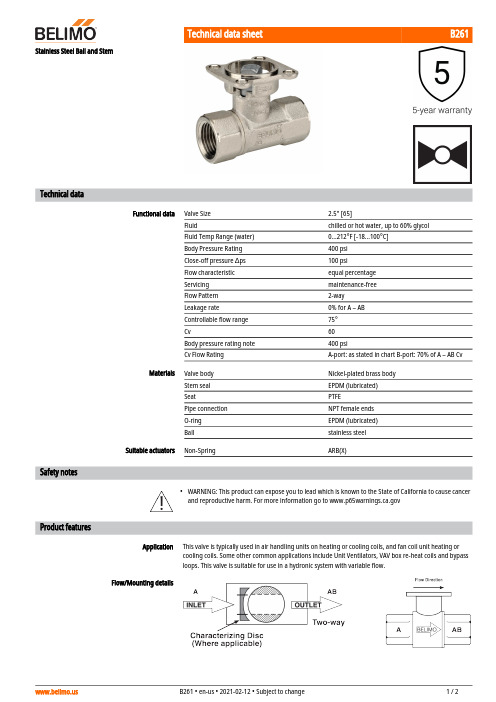
B261•ApplicationStainless Steel Ball and StemTechnical dataFunctional dataValve Size 2.5" [65]Fluidchilled or hot water, up to 60% glycol Fluid Temp Range (water)0...212°F [-18...100°C]Body Pressure Rating 400 psi Close-off pressure ∆ps 100 psiFlow characteristic equal percentage Servicing maintenance-free Flow Pattern 2-way Leakage rate0% for A – AB Controllable flow range 75°Cv60 Body pressure rating note 400 psiCv Flow RatingA-port: as stated in chart B-port: 70% of A – AB Cv MaterialsValve body Nickel-plated brass body Stem seal EPDM (lubricated)SeatPTFEPipe connection NPT female ends O-ring EPDM (lubricated)Ballstainless steel Suitable actuatorsNon-SpringARB(X)Safety notesWARNING: This product can expose you to lead which is known to the State of California to cause cancer and reproductive harm. For more information go to Product featuresThis valve is typically used in air handling units on heating or cooling coils, and fan coil unit heating or cooling coils. Some other common applications include Unit Ventilators, VAV box re-heat coils and bypass loops. This valve is suitable for use in a hydronic system with variable flow.Flow/Mounting detailsB261 DimensionsDimensional drawingsARB, ARXA B C D E F H110.1" [257] 5.6" [141]8.0" [203] 6.0" [152] 2.8" [71] 2.8" [71] 1.9" [48]AFRB, AFRXA B C D E F11.5" [293] 5.6" [141]8.6" [219] 6.6" [168] 2.0" [51] 2.0" [51]ARQB, ARQXA B C D E F H1H29.9" [251] 4.2" [107]8.1" [206] 6.1" [155] 2.3" [58] 2.3" [58]0.8" [20]0.6" [15]AFRB N4, AFRX N4A B D E F11.4" [289] 5.6" [141]8.0" [203] 2.4" [62] 2.4" [62]ARB N4, ARX N4, NRB N4, NRX N4A B D E F11.4" [289] 5.6" [141]8.0" [203] 3.1" [80] 3.1" [80]A B C D E F H1H29.9" [251] 4.2" [107]8.1" [206] 6.1" [155] 2.3" [58] 2.3" [58]0.8" [20]0.6" [15]A B D E F11.4" [289] 5.6" [141]8.0" [203] 3.1" [80] 3.1" [80]AFRB24-S On/Off, Spring Return, AC/DC 24 VTechnical dataElectrical data Nominal voltage AC/DC 24 VNominal voltage frequency50/60 HzPower consumption in operation 5 WPower consumption in rest position 2.5 WTransformer sizing7.5 VA (class 2 power source)Auxiliary switch 2 x SPDT, 3 A resistive (0.5 A inductive) @ AC 250 V,one set at 10°, one adjustable 10...90°Switching capacity auxiliary switch 3 A resistive (0.5 A inductive) @ AC 250 VElectrical Connection(2) 18 GA appliance cables with 1/2" conduitconnectors, 3 ft [1 m],Overload Protection electronic throughout 0...95° rotationFunctional data Direction of motion motor selectable by ccw/cw mountingDirection of motion fail-safe reversible with cw/ccw mountingManual override 5 mm hex crank (3/16" Allen), suppliedAngle of rotation90°Running Time (Motor)75 sRunning time fail-safe<20 sNoise level, motor45 dB(A)Noise level, fail-safe62 dB(A)Position indication MechanicalSafety data Degree of protection IEC/EN IP54Degree of protection NEMA/UL NEMA 2 UL Enclosure Type 2Agency Listing cULus acc. to UL60730-1A/-2-14, CAN/CSAE60730-1:02, CE acc. to 2014/30/EU and 2014/35/EU; Listed to UL 2043 - suitable for use in airplenums per Section 300.22(c) of the NEC andSection 602.2 of the IMCQuality Standard ISO 9001Ambient temperature-22...122°F [-30...50°C]Storage temperature-40...176°F [-40...80°C]Ambient humidity max. 95% r.H., non-condensingServicing maintenance-freeWeight Weight 5.7 lb [2.6 kg]Electrical installationINSTALLATION NOTESActuators with appliance cables are numbered.Provide overload protection and disconnect as required.AFRB24-STwo built-in auxiliary switches (2x SPDT), for end position indication, interlock control, fan startup, etc.Actuators may be powered in parallel. Power consumption must be observed.Parallel wiring required for piggy-back applications.Apply only AC line voltage or only UL-Class 2 voltage to the terminals of auxiliary switches. Mixed orcombined operation of line voltage/safety extra low voltage is not allowed.Meets cULus requirements without the need of an electrical ground connection.Warning! Live Electrical Components!During installation, testing, servicing and troubleshooting of this product, it may be necessary to workwith live electrical components. Have a qualified licensed electrician or other individual who has beenproperly trained in handling live electrical components perform these tasks. Failure to follow all electricalsafety precautions when exposed to live electrical components could result in death or serious injury.On/Off Auxiliary Switches。
XJ261系列说明书Ver1.1
本手册不适用于未受训者,维护、安装工作只能由有资质的人员 完成。
II
XJ261 系列电力网络仪表 用户手册
目录
一、产品简介........................................................................................................................................... 2 二、技术参数........................................................................................................................................... 2 三、安装................................................................................................................................................... 3
AT26DF321资料

Features Array•Single 2.7V - 3.6V Supply•Serial Peripheral Interface (SPI) Compatible–Supports SPI Modes 0 and 3•66 MHz Maximum Clock Frequency•Flexible, Uniform Erase Architecture–4-Kbyte Blocks–32-Kbyte Blocks–64-Kbyte Blocks–Full Chip Erase•Individual Sector Protection with Global Protect/Unprotect Feature–Sixty-Four 64-Kbyte Physical Sectors•Hardware Controlled Locking of Protected Sectors•Flexible Programming–Byte/Page Program (1 to 256 Bytes)•JEDEC Standard Manufacturer and Device ID Read Methodology•Low Power Dissipation–7 mA Active Read Current (Typical)–4 µA Deep Power-Down Current (Typical)•Endurance: 100,000 Program/Erase Cycles•Data Retention: 20 Years•Complies with Full Industrial Temperature Range•Industry Standard Green (Pb/Halide-free/RoHS Compliant) Package Options –8-lead SOIC (200-mil wide)–16-lead SOIC (300-mil wide)1.DescriptionThe AT26DF321 is a serial interface Flash memory device designed for use in a wide variety of high-volume consumer based applications in which program code is shad-owed from Flash memory into embedded or external RAM for execution. The flexible erase architecture of the AT26DF321, with its erase granularity as small as 4-Kbytes, makes it ideal for data storage as well, eliminating the need for additional data storage EEPROM devices.The physical sectoring and the erase block sizes of the AT26DF321 have been opti-mized to meet the needs of today's code and data storage applications. By optimizing the size of the physical sectors and erase blocks, the memory space can be used much more efficiently. Because certain code modules and data storage segments must reside by themselves in their own protected sectors, the wasted and unused memory space that occurs with large sectored and large block erase Flash memory devices can be greatly reduced. This increased memory space efficiency allows addi-tional code routines and data storage segments to be added while still maintaining thesame overall device density.23633C–DFLASH–08/06AT26DF321 [Preliminary]The AT26DF321 also offers a sophisticated method for protecting individual sectors against erroneous or malicious program and erase operations. By providing the ability to individually pro-tect and unprotect sectors, a system can unprotect a specific sector to modify its contents while keeping the remaining sectors of the memory array securely protected. This is useful in applica-tions where program code is patched or updated on a subroutine or module basis, or in applications where data storage segments need to be modified without running the risk of errant modifications to the program code segments. In addition to individual sector protection capabili-ties, the AT26DF321 incorporates Global Protect and Global Unprotect features that allow the entire memory array to be either protected or unprotected all at once. This reduces overhead during the manufacturing process since sectors do not have to be unprotected one-by-one prior to initial programming.Specifically designed for use in 3-volt systems, the AT26DF321 supports read, program, and erase operations with a supply voltage range of 2.7V to 3.6V. No separate voltage is required for programming and erasing.2.Pin Descriptions and PinoutsTable 2-1.Pin DescriptionsSymbolName and FunctionAsserted StateTypeCS CHIP SELECT : Asserting the CS pin selects the device. When the CS pin is deasserted, thedevice will be deselected and normally be placed in standby mode (not Deep Power-Down mode), and the SO pin will be in a high-impedance state. When the device is deselected, data will not be accepted on the SI pin.A high-to-low transition on the CS pin is required to start an operation, and a low-to-high transition is required to end an operation. When ending an internally self-timed operation such as a program or erase cycle, the device will not enter the standby mode until the completion of the operation.Low InputSCK SERIAL CLOCK : This pin is used to provide a clock to the device and is used to control the flow of data to and from the device. Command, address, and input data present on the SI pin is always latched on the rising edge of SCK, while output data on the SO pin is always clocked out on the falling edge of SCK.InputSI SERIAL INPUT : The SI pin is used to shift data into the device. The SI pin is used for all data input including command and address sequences. Data on the SI pin is always latched on the rising edge of SCK.InputSO SERIAL OUTPUT : The SO pin is used to shift data out from the device. Data on the SO pin is always clocked out on the falling edge of SCK.OutputWP WRITE PROTECT : The WP pin controls the hardware locking feature of the device. Please refer to “Protection Commands and Features” on page 11 for more details on protection features and the WP pin.The WP pin is internally pulled-high and may be left floating if hardware controlled protection will not be used. However, it is recommended that the WP pin also be externally connected to V CC whenever possible.Low InputV CC DEVICE POWER SUPPLY : The V CC pin is used to supply the source voltage to the device.Operations at invalid V CC voltages may produce spurious results and should not be attempted.Power GNDGROUND : The ground reference for the power supply. GND should be connected to the system ground.Power33633C–DFLASH–08/06AT26DF321 [Preliminary]3.Block Diagram4.Memory ArrayTo provide the greatest flexibility, the memory array of the AT26DF321 can be erased in four lev-els of granularity including a full chip erase. In addition, the array has been divided into physical sectors of uniform size, of which each sector can be individually protected from program and erase operations. The size of the physical sectors is optimized for both code and data storage applications, allowing both code and data segments to reside in their own isolated regions.Figure 4-1 on page 4 illustrates the breakdown of each erase level as well as the break-down of each physical sector.Figure 2-1.8-SOIC Top ViewFigure 2-2.16-SOIC Top View43633C–DFLASH–08/06AT26DF321 [Preliminary]Figure 4-1.Memory Architecture Diagram53633C–DFLASH–08/06AT26DF321 [Preliminary]5.Device OperationThe AT26DF321 is controlled by a set of instructions that are sent from a host controller, com-monly referred to as the SPI Master. The SPI Master communicates with the AT26DF321 via the SPI bus which is comprised of four signal lines: Chip Select (CS), Serial Clock (SCK), Serial Input (SI), and Serial Output (SO).The SPI protocol defines a total of four modes of operation (mode 0, 1, 2, or 3) with each mode differing in respect to the SCK polarity and phase and how the polarity and phase control the flow of data on the SPI bus. The AT26DF321 supports the two most common modes, SPI Modes 0 and 3. The only difference between SPI Modes 0 and 3 is the polarity of the SCK signal when in the inactive state (when the SPI Master is in standby mode and not transferring any data). With SPI Modes 0 and 3, data is always latched in on the rising edge of SCK and always output on the falling edge of SCK.Figure 5-1.SPI Mode 0 and 3mands and Addressingpin has been asserted, the SPI Master must then clock out a valid 8-bit opcode on the SPI bus.Following the opcode, instruction dependent information such as address and data bytes would then be clocked out by the SPI Master. All opcode, address, and data bytes are transferred with Opcodes not supported by the AT26DF321 will be ignored by the device and no operation will be started. The device will continue to ignore any data presented on the SI pin until the start of the next operation (CS pin being deasserted and then reasserted). In addition, if the CS pin is deas-serted before complete opcode and address information is sent to the device, then no operation will be performed and the device will simply return to the idle state and wait for the next operation.Addressing of the device requires a total of three bytes of information to be sent, representing address bits A23-A0. Since the upper address limit of the AT26DF321 memory array is 3FFFFFh, address bits A23-A22 are always ignored by the device.63633C–DFLASH–08/06AT26DF321 [Preliminary]Table 6-1.Command ListingCommandOpcodeAddress BytesDummy BytesData BytesRead CommandsRead Array0Bh 0000 1011311+Read Array (Low Frequency)03h0000 001131+Program and Erase CommandsBlock Erase (4-KBytes)20h 0010 0000300Block Erase (32-KBytes)52h 0101 0010300Block Erase (64-KBytes)D8h 1101 1000300Chip Erase60h 0110 0000000C7h 1100 0111000Byte/Page Program (1 to 256 Bytes)02h0000 001031+Protection CommandsWrite Enable 06h 0000 0110000Write Disable 04h 0000 0100000Protect Sector 36h 0011 0110300Unprotect Sector 39h0011 10013Global Protect/Unprotect Use Write Status Register commandRead Sector Protection Registers 3Ch 0011 110031+Status Register CommandsRead Status Register 05h 0000 0101001+Write Status Register 01h0000 00011Miscellaneous CommandsRead Manufacturer and Device ID 9Fh 1001 111100 1 to 4Deep Power-DownB9h 1011 1001000Resume from Deep Power-DownABh1010 101173633C–DFLASH–08/06AT26DF321 [Preliminary]7.Read Commands7.1Read ArrayThe Read Array command can be used to sequentially read a continuous stream of data from the device by simply providing the SCK signal once the initial starting address has been speci-fied. The device incorporates an internal address counter that automatically increments on every clock cycle.Two opcodes, 0Bh and 03h, can be used for the Read Array command. The use of each opcode depends on the maximum SCK frequency that will be used to read data from the device. The 0Bh opcode can be used at any SCK frequency up to the maximum specified by f SCK . The 03h opcode can be used for lower frequency read operations up to the maximum specified by f RDLF .To perform the Read Array operation, the CS pin must first be asserted and the appropriate opcode (0Bh or 03h) must be clocked into the device. After the opcode has been clocked in, the three address bytes must be clocked in to specify the starting address location of the first byte to read within the memory array. If the 0Bh opcode is used, then one don’t care byte must also be clocked in after the three address bytes.After the three address bytes (and the one don’t care byte if using opcode 0Bh) have been clocked in, additional clock cycles will result in serial data being output on the SO pin. The data is always output with the MSB of a byte first. When the last byte (3FFFFFh) of the memory array has been read, the device will continue reading back at the beginning of the array (000000h). No delays will be incurred when wrapping around from the end of the array to the beginning of the array.ance state. The CS pin can be deasserted at any time and does not require that a full byte of data be read.Figure 7-1.Read Array – 0Bh OpcodeFigure 7-2.Read Array – 03h Opcode83633C–DFLASH–08/06AT26DF321 [Preliminary]8.Program and Erase Commands8.1Byte/Page ProgramThe Byte/Page Program command allows anywhere from a single byte of data to 256 bytes of data to be programmed into previously erased memory locations. An erased memory location is one that has all eight bits set to the logical “1” state (a byte value of FFh). Before a Byte/Page Program command can be started, the Write Enable command must have been previously issued to the device (see Write Enable command description) to set the Write Enable Latch (WEL) bit of the Status Register to a logical “1” state.To perform a Byte/Page Program command, an opcode of 02h must be clocked into the device followed by the three address bytes denoting the first byte location of the memory array to begin programming at. After the address bytes have been clocked in, data can then be clocked into the device and will be stored in an internal buffer.If the starting memory address denoted by A23-A0 does not fall on an even 256-byte page boundary (A7-A0 are not all 0), then special circumstances regarding which memory locations will be programmed will apply. In this situation, any data that is sent to the device that goes beyond the end of the page will wrap around back to the beginning of the same page. For exam-ple, if the starting address denoted by A23-A0 is 0000FEh, and three bytes of data are sent to the device, then the first two bytes of data will be programmed at addresses 0000FEh and 0000FFh while the last byte of data will be programmed at address 000000h. The remaining bytes in the page (addresses 000001h through 0000FDh) will be unaffected and will not change.In addition, if more than 256 bytes of data are sent to the device, then only the last 256 bytes sent will be latched into the internal buffer.When the CS pin is deasserted, the device will take the data stored in the internal buffer and pro-gram it into the appropriate memory array locations based on the starting address specified by A23-A0 and the number of complete data bytes sent to the device. If less than 256 bytes of data were sent to the device, then the remaining bytes within the page will not be altered. The pro-gramming of the data bytes is internally self-timed and should take place in a time of t PP .The three address bytes and at least one complete byte of data must be clocked into the device before the CS pin is deasserted; otherwise, the device will abort the operation and no data will be programmed into the memory array. In addition, if the address specified by A23-A0 points to a memory location within a sector that is in the protected state (see “Protect Sector” on page 12), then the Byte/Page Program command will not be executed, and the device will return to the idle state once the CS pin has been deasserted. The WEL bit in the Status Register will be reset back to the logical “0” state if the program cycle aborts due to an incomplete address being sent,an incomplete byte of data being sent, or because the memory location to be programmed is protected.While the device is programming, the Status Register can be read and will indicate that the device is busy. For faster throughput, it is recommended that the Status Register be polled rather than waiting the t PP time to determine if the data bytes have finished programming. At some point before the program cycle completes, the WEL bit in the Status Register will be reset back to the logical “0” state.93633C–DFLASH–08/06AT26DF321 [Preliminary]Figure 8-1.Byte ProgramFigure 8-2.Page Program8.2Block EraseA block of 4K-, 32K-, or 64K-bytes can be erased (all bits set to the logical “1” state) in a single operation by using one of three different opcodes for the Block Erase command. An opcode of 20h is used for a 4K-byte erase, an opcode of 52h is used for a 32K-byte erase, and an opcode of D8h is used for a 64K-byte erase. Before a Block Erase command can be started, the Write Enable command must have been previously issued to the device to set the WEL bit of the Sta-tus Register to a logical “1” state.52h, or D8h) must be clocked into the device. After the opcode has been clocked in, the three address bytes specifying an address within the 4K-, 32K-, or 64K-byte block to be erased must be clocked in. Any additional data clocked into the device will be ignored. When the CS pin is deasserted, the device will erase the appropriate block. The erasing of the block is internally self-timed and should take place in a time of t BLKE .Since the Block Erase command erases a region of bytes, the lower order address bits do not need to be decoded by the device. Therefore, for a 4K-byte erase, address bits A11-A0 will be ignored by the device and their values can be either a logical “1” or “0”. For a 32K-byte erase,address bits A14-A0 will be ignored, and for a 64K-byte erase, address bits A15-A0 will be ignored by the device. Despite the lower order address bits not being decoded by the device, the complete three address bytes must still be clocked into the device before the CS pin is deas-serted; otherwise, the device will abort the operation and no erase operation will be performed.103633C–DFLASH–08/06AT26DF321 [Preliminary]If the address specified by A23-A0 points to a memory location within a sector that is in the pro-tected state, then the Block Erase command will not be executed, and the device will return to The WEL bit in the Status Register will be reset back to the logical “0” state if the erase cycle aborts due to an incomplete address being sent or because a memory location within the region to be erased is protected.While the device is executing a successful erase cycle, the Status Register can be read and will indicate that the device is busy. For faster throughput, it is recommended that the Status Regis-ter be polled rather than waiting the t BLKE time to determine if the device has finished erasing. At some point before the erase cycle completes, the WEL bit in the Status Register will be reset back to the logical “0” state.Figure 8-3.Block Erase8.3Chip EraseThe entire memory array can be erased in a single operation by using the Chip Erase command.Before a Chip Erase command can be started, the Write Enable command must have been pre-viously issued to the device to set the WEL bit of the Status Register to a logical “1” state.Two opcodes, 60h and C7h, can be used for the Chip Erase command. There is no difference in device functionality when utilizing the two opcodes, so they can be used interchangeably. To perform a Chip Erase, one of the two opcodes (60h or C7h) must be clocked into the device.Since the entire memory array is to be erased, no address bytes need to be clocked into the device, and any data clocked in after the opcode will be ignored. When the CS pin is deasserted,the device will erase the entire memory array. The erasing of the device is internally self-timed and should take place in a time of t CHPE .wise, no erase will be performed. In addition, if any sector of the memory array is in the protected state, then the Chip Erase command will not be executed, and the device will return to the idle state once the CS pin has been deasserted. The WEL bit in the Status Register will be reset back to the logical “0” state if a sector is in the protected state.While the device is executing a successful erase cycle, the Status Register can be read and will indicate that the device is busy. For faster throughput, it is recommended that the Status Regis-ter be polled rather than waiting the t CHPE time to determine if the device has finished erasing. At some point before the erase cycle completes, the WEL bit in the Status Register will be reset back to the logical “0” state.AT26DF321 [Preliminary] Figure 8-4.Chip Erase9.Protection Commands and Features9.1Write EnableThe Write Enable command is used to set the Write Enable Latch (WEL) bit in the Status Regis-ter to a logical “1” state. The WEL bit must be set before a program, erase, Protect Sector,Unprotect Sector, or Write Status Register command can be executed. This makes the issuanceof these commands a two step process, thereby reducing the chances of a command beingaccidentally or erroneously executed. If the WEL bit in the Status Register is not set prior to theissuance of one of these commands, then the command will not be executed.must be clocked into the device. No address bytes need to be clocked into the device, and anythe Status Register will be set to a logical “1”. The complete opcode must be clocked into thestate of the WEL bit will not change.Figure 9-1.Write Enable9.2Write DisableThe Write Disable command is used to reset the Write Enable Latch (WEL) bit in the Status Reg-ister to the logical “0” state. With the WEL bit reset, all program, erase, Protect Sector, UnprotectSector, and Write Status Register commands will not be executed. The Write Disable commandis also used to exit the Sequential Program Mode. Other conditions can also cause the WEL bitto be reset; for more details, refer to the WEL bit section of the Status Register description onpage 20.must be clocked into the device. No address bytes need to be clocked into the device, and anythe Status Register will be reset to a logical “0”. The complete opcode must be clocked into thestate of the WEL bit will not change.Figure 9-2.Write Disable9.3Protect SectorEvery physical sector of the device has a corresponding single-bit Sector Protection Registerthat is used to control the software protection of a sector. Upon device power-up or after adevice reset, each Sector Protection Register will default to the logical “1” state indicating that allsectors are protected and cannot be programmed or erased.Issuing the Protect Sector command to a particular sector address will set the correspondingSector Protection Register to the logical “1” state. The following table outlines the two states ofthe Sector Protection Registers.Table 9-1.Sector Protection Register ValuesValue Sector Protection Status0Sector is unprotected and can be programmed and erased.1Sector is protected and cannot be programmed or erased. This is the default state.Before the Protect Sector command can be issued, the Write Enable command must have beenpreviously issued to set the WEL bit in the Status Register to a logical “1”. To issue the ProtectSector command, the CS pin must first be asserted and the opcode of 36h must be clocked intothe device followed by three address bytes designating any address within the sector to belocked. Any additional data clocked into the device will be ignored. When the CS pin is deas-serted, the Sector Protection Register corresponding to the physical sector addressed by A23-A0 will be set to the logical “1” state, and the sector itself will then be protected from programAT26DF321 [Preliminary] and erase operations. In addition, the WEL bit in the Status Register will be reset back to the log-ical “0” state.serted; otherwise, the device will abort the operation, the state of the Sector Protection Registerwill be unchanged, and the WEL bit in the Status Register will be reset to a logical “0”.As a safeguard against accidental or erroneous protecting or unprotecting of sectors, the SectorProtection Registers can themselves be locked from updates by using the SPRL (Sector Protec-tion Registers Locked) bit of the Status Register (please refer to “Status Register Commands”on page 19 for more details). If the Sector Protection Registers are locked, then any attempts toissue the Protect Sector command will be ignored, and the device will reset the WEL bit in thedeasserted.Figure 9-3.Protect Sector9.4Unprotect SectorIssuing the Unprotect Sector command to a particular sector address will reset the correspond-ing Sector Protection Register to the logical “0” state (see Table 9-1 on page 12 for SectorProtection Register values). Every physical sector of the device has a corresponding single-bitSector Protection Register that is used to control the software protection of a sector.Before the Unprotect Sector command can be issued, the Write Enable command must havebeen previously issued to set the WEL bit in the Status Register to a logical “1”. To issue theUnprotect Sector command, the CS pin must first be asserted and the opcode of 39h must beclocked into the device. After the opcode has been clocked in, the three address bytes designat-ing any address within the sector to be unlocked must be clocked in. Any additional data clockedtor Protection Register corresponding to the sector addressed by A23-A0 will be reset to thelogical “0” state, and the sector itself will be unprotected. In addition, the WEL bit in the StatusRegister will be reset back to the logical “0” state.serted; otherwise, the device will abort the operation, the state of the Sector Protection Registerwill be unchanged, and the WEL bit in the Status Register will be reset to a logical “0”.As a safeguard against accidental or erroneous locking or unlocking of sectors, the Sector Pro-tection Registers can themselves be locked from updates by using the SPRL (Sector ProtectionRegisters Locked) bit of the Status Register (please refer to “Status Register Commands” onpage 19 for more details). If the Sector Protection Registers are locked, then any attempts toissue the Unprotect Sector command will be ignored, and the device will reset the WEL bit in theStatus Register back to a logical “0” and return to the idle state once the CS pin has beendeasserted.Figure 9-4.Unprotect Sector9.5Global Protect/UnprotectThe Global Protect and Global Unprotect features can work in conjunction with the Protect Sec-tor and Unprotect Sector functions. For example, a system can globally protect the entirememory array and then use the Unprotect Sector command to individually unprotect certain sec-tors and individually reprotect them later by using the Protect Sector command. Likewise, asystem can globally unprotect the entire memory array and then individually protect certain sec-tors as needed.Performing a Global Protect or Global Unprotect is accomplished by writing a certain combina-tion of data to the Status Register using the Write Status Register command (see “Write StatusRegister” section on page 21 for command execution details). The Write Status Register com-mand is also used to modify the SPRL (Sector Protection Registers Locked) bit to controlhardware and software locking.To perform a Global Protect, the appropriate WP pin and SPRL conditions must be met and thesystem must write a logical “1” to bits 5, 4, 3, and 2 of the Status Register. Conversely, to per-form a Global Unprotect, the same WP and SPRL conditions must be met but the system mustwrite a logical “0” to bits 5, 4, 3, and 2 of the Status Register. Table 9-2 details the conditionsnecessary for a Global Protect or Global Unprotect to be performed.AT26DF321 [Preliminary]Essentially, if the SPRL bit of the Status Register is in the logical “0” state (Sector Protection Registers are not locked), then writing a 00h to the Status Register will perform a Global Unpro-tect without changing the state of the SPRL bit. Similarly, writing a 7Fh to the Status Register will perform a Global Protect and keep the SPRL bit in the logical “0” state. The SPRL bit can, of course, be changed to a logical “1” by writing an FFh if software-locking or hardware-locking is desired along with the Global Protect.Table 9-2.Valid SPRL and Global Protect/Unprotect ConditionsWP StateCurrent SPRL Value New Write Status Register Data Protection OperationNew SPRL Value Bit7 6 5 4 3 2 1 000 x 0 0 0 0 x x 0 x 0 0 0 1 x x↕0 x 1 1 1 0 x x 0 x 1 1 1 1 x x1 x 0 0 0 0 x x 1 x 0 0 0 1 x x↕1 x 1 1 1 0 x x 1 x 1 1 1 1 x xGlobal Unprotect – all Sector Protection Registers reset to 0No change to current protection.No change to current protection.No change to current protection.Global Protect – all Sector Protection Registers set to 1Global Unprotect – all Sector Protection Registers reset to 0No change to current protection.No change to current protection.No change to current protection.Global Protect – all Sector Protection Registers set to 100000111111x x x x x x x xNo change to the current protection level. All sectors currentlyprotected will remain protected and all sectors currently unprotected will remain unprotected.The Sector Protection Registers are hard-locked and cannot bechanged when the WP pin is LOW and the current state of SPRL is 1. Therefore, a Global Protect/Unprotect will not occur. In addition, the SPRL bit cannot be changed (the WP pin must be HIGH in order to change SPRL back to a 0).10 x 0 0 0 0 x x 0 x 0 0 0 1 x x↕0 x 1 1 1 0 x x 0 x 1 1 1 1 x x1 x 0 0 0 0 x x 1 x 0 0 0 1 x x↕1 x 1 1 1 0 x x 1 x 1 1 1 1 x x Global Unprotect – all Sector Protection Registers reset to 0No change to current protection.No change to current protection.No change to current protection.Global Protect – all Sector Protection Registers set to 1Global Unprotect – all Sector Protection Registers reset to 0No change to current protection.No change to current protection.No change to current protection.Global Protect – all Sector Protection Registers set to 10000011111110 x 0 0 0 0 x x 0 x 0 0 0 1 x x↕0 x 1 1 1 0 x x 0 x 1 1 1 1 x x1 x 0 0 0 0 x x 1 x 0 0 0 1 x x↕1 x 1 1 1 0 x x 1 x 1 1 1 1 x xNo change to the current protection level. All sectors currently protected will remain protected, and all sectors currently unprotected will remain unprotected.The Sector Protection Registers are soft-locked and cannot be changed when the current state of SPRL is 1. Therefore, a Global Protect/Unprotect will not occur. However, theSPRL bit can be changed back to a 0 from a 1 since the WP pin is HIGH. To perform a Global Protect/Unprotect, the Write Status Register command must be issued again after the SPRL bit has been changed from a 1 to a 0.0000011111。
ASTM A262-02中文翻译(自己翻译的)
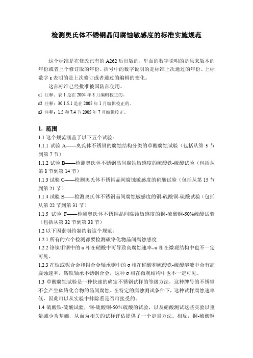
检测奥氏体不锈钢晶间腐蚀敏感度的标准实施规范这个标准是在修改已有的A262后出版的,里面的数字说明的是原来版本的年份或者上个修订版的年份。
括号中的数字说明的是标准上次通过的年份。
上标数字ε表明的是上次修订或者通过的编辑的变化。
这部标准已经批准被国防部使用。
ε1 注释:表1是在2004年8月编辑校正的。
ε2 注释:30.1.5.1是在2005年1月编辑校正的。
ε3 注释:1.5和7.4节2005年7月编辑校正。
1. 范围1.1这个规范涵盖了以下五个试验:1.1.1试验A——奥氏体不锈钢的腐蚀结构分类的草酸腐蚀试验(包括从第3节到第7节)1.1.2试验B——检测奥氏体不锈钢晶间腐蚀敏感度的硫酸铁-硫酸试验(包括从第8节到第14节)1.1.3试验C——检测奥氏体不锈钢晶间腐蚀敏感度的硝酸试验(包括从第15节到第21节)1.1.4试验E——检测奥氏体不锈钢晶间腐蚀敏感度的铜-硫酸铜-硫酸试验(包括从第22节到第31节)1.1.5试验F——检测奥氏体不锈钢晶间腐蚀敏感度的铜-硫酸铜-50%硫酸试验(包括从第32节到第38节)1.2以下因素制约制约着这个规范:1.2.1所有的六个检测都要检测碳铬化物晶间腐蚀感度1.2.2铬镍钼钢中的σ相在硝酸中可导致高腐蚀速率,σ相在微观结构中也不一定可见。
1.2.3在钛或铌合金和钼合金轴承钢中的σ相在硝酸和硫酸铁-硫酸溶液中会有高腐蚀速率,铸铁轴承不锈钢合金,这种σ相在微观结构中也不一定可见。
1.3草酸腐蚀试验是一种快速的确定不锈钢试样的等级方法,这种牌号的不锈钢不会产生碳铬化合物的晶间腐蚀。
在特定的腐蚀测试条件下,这种试样腐蚀速率低,因此可以从实验中排除看是否可接受的。
1.4硫酸铁-硫酸试验,铜-硫酸铜-50%硫酸的试验,以及硝酸测试这些实验以重量减少为基础,从而为相关的试样评估提供了一个定量方法。
相反,铜-硫酸铜-16%硫酸试验主要对弯曲试样进行表观检查,因此只能确定试样是否合格。
摩斯阿电子V2616系列嵌入式计算机介绍说明书

IntroductionV2616 Series embedded computers are based on the Intel Core 2 Duo x86 processor, and feature 2 RS-232/422/485 serial ports, dual LAN ports, and 3 USB 2.0 hosts. V2616 computers also provide VGA and DVI-I outputs, and are also compliant with a portion of EN 50155 specifications, covering operating temperature, power input voltage, power surges, ESD, and vibration, making them particularly well-suited for railway and industrial applications.The V2616's CompactFlash socket and internal SATA II storage tray provide these computers with the reliability needed for industrialapplications that require data buffering and storage expansion. Most importantly, the V2616 computers come with 2 removable slots for inserting additional storage media, such as hard disks or SSD drives, and can offer RAID 0 and RAID 1 functions for data reliability.The V2616 series come pre-installed with Linux or WindowsEmbedded Standard 2009 to provide programmers with a familiar environment in which to develop sophisticated, bug-free application software at a low cost.AppearanceFront ViewCompactFlash (Storage, Power)Seria/LAN Serial/LANRear ViewHardware SpecificationsComputerCPU: Intel Core 2 Duo SP9300, dual core 64 bit threaded 2.26 GHz, 6 MB for L2 cacheSystem Chipset: Intel GS45 + ICH9-M FSB: 1066System Memory: 4 GB capacity, 2 GB pre-installed: 2 slots of 2 GB DDR3-1066 200 pin SO-DIMM SDRAMUSB: 3 USB 2.0 compliant hosts; 2 with type A connectors supporting system bootup, 1 with M12 connectorOS (pre-installed): Linux, or Windows Embedded Standard 2009StorageBuilt-in: 2 GB onboard industrial CompactFlash card, for root file systemStorage Device Support:• 2 removable drive trays, for 2.5” SSD or HDD• (Optional) Internal SATA II drive slot, for 2.5” SSD or HDDOther PeripheralsKB/MS: 1 PS/2 interface supporting standard PS/2 keyboard and mouse through Y-type cable Audio: Line-in, line-out interfaceDisplayGraphics Controller: Intel GS45 integrated graphics engine DVI Interface: DVI-D connector (chrontel CH7307 SDVO to DVI transmitter), up to 1600 x 1200 resolutionVGA Interface: DB15 female connector, up to 2048 x 1536 resolutionEthernet Interface LAN: 2 auto-sensing 10/100/1000 Mbps ports (M12)Serial InterfaceSerial Standards: 2 software-selectable RS-232/422/485 ports* (DB9 male)Optical Isolation Protection: 2 kV ESD Protection: 4 kV for all signalsMagnetic Isolation Protection: 1.5 kV built-inSerial Communication ParametersData Bits: 5, 6, 7, 8Stop Bits: 1, 1.5, 2Parity: None, Even, Odd, Space, MarkFlow Control: RTS/CTS, XON/XOFF, ADDC® (automatic data direction control) for RS-485Baudrate: 50 bps to 921.6 kbps (non-standard baudrates supported; see user’s manual for details)Serial SignalsRS-232: TxD, RxD, DTR, DSR, RTS, CTS, DCD, GND RS-422: TxDA(-), TxDB(+), RxDB(+), RxDA(-), GND RS-485-4w: TxDA(-), TxDB(+), RxDB(+), RxDA(-), GND RS-485-2w: DataA(-), DataB(+), GNDDigital InputInput Channels: 6, source type Input Voltage: 0 to 30 VDC at 25 Hz Digital Input Levels for Dry Contacts: • Logic level 0: Close to GND • Logic level 1: OpenDigital Input Levels for Wet Contacts: • Logic level 0: +3 V max.• Logic level 1: +10 V to +30 V (Source to DI)Isolation: 3 kV optical isolationDigital OutputOutput Channels: 2, sink typeOutput Current: Max. 200 mA per channelOn-state Voltage: 24 VDC nominal, open collector to 30 VDC Connector Type: 10-pin screw terminal block (6 DI points, 2 DO points, DI Source, GND)Isolation: 3 kV optical isolationLEDsSystem: Power x 1, Storage x 1LAN: 100M/Link x 2, 1000M/Link x 2Serial: TX x 2, RX x 2Physical CharacteristicsHousing: Aluminum Weight: 5 kg Dimensions:Without ears: 287 x 250 x 101 mm (11.29 x 9.84 x 3.97 in) With ears: 287 x 290 x 101 mm (11.29 x 11.41 x 3.97 in)Mounting: wallEnvironmental LimitsOperating Temperature: (with SSD installed) -25 to 55°C (-13 to 140°F)Storage Temperature: (with SSD installed) -30 to 60°C (-40 to 185°F)DVI-D OutputAudio Input OutputLAN Port x 2 (M12)Host (M12)Pin Assignment (Reserved for RF SMA type)Serial Port x 2(RS-232/422/485)Ambient Relative Humidity: 5 to 95% (non-condensing)Anti-vibration: EN 50155 standardAnti-shock: EN 50155 standardConformal Coating: Available on requestPower RequirementsInput Voltage: 24 VDC (9 to 36 V), M12 connectorNote: 24 VDC is EN 50155 compliantPower Consumption: 50 W• 2 A @ 24 VDCPower Button: On/off (front panel)Standards and CertificationsSafety: UL 60950-1, CSA C22.2 No. 60950-1-07, EN 60950-1 EMC: EN 55022 Class A, EN 61000-3-2 Class D, EN 61000-3-3, EN 55024, FCC Part 15 Subpart B Class A Green Product: RoHS, CRoHS, WEEERail Traffic: EN 50155*, EN 50121-2-3, EN 50121-4, IEC 61373*Complies with a portion of EN 50155 specifications. Please contact Moxa or a Moxa distributor for details.ReliabilityAutomatic Reboot Trigger: Built-in WDT (watchdog timer) supporting 1-255 level time interval system reset, software programmable WarrantyWarranty Period: 3 yearsDetails: See /warrantyNote: These hardware specifications describe the embedded computer unit itself, but not its official accessories. In particular, the wide temperature specification does not apply to accessories such as power adapters and cables.Software SpecificationsLinuxOS: Debian Linux 5.0, “Lenny”, kernel 2.6.32File System: EXT2/EXT3Internet Protocol Suite: TCP, UDP, IPv4, SNMPv1/v2c/v3, ICMP, ARP, HTTP, CHAP, PAP, SSH 1.0/2.0, SSL, DHCP, NTP, NFS, Telnet, FTP, TFTP, PPP, PPPoEInternet Security: OpenVPN, iptables firewallWeb Server (Apache): Allows you to create and manage web sites; supports PHP and XMLTerminal Server (SSH): Provides secure encrypted communications between two un-trusted hosts over an insecure networkDial-up Networking: PPP (Linux) allows machines to connect to the Internet through dialup lines as either PPP server or client. Works with ‘chat’, ‘dip’, and ‘diald’, among (many) others. Supports IP, TCP, UDP, and Novell IPX.File Server: Enables remote clients to access files and other resources over the networkWatchdog: Features a hardware function to trigger system reset in a user specified time interval (Moxa API provided)Application Development Software:• Moxa API library (Watchdog timer, Moxa serial I/O control, Moxa DI/ DO API)• GNU C/C++ compiler• GNU C library• PerlWindows XP EmbeddedOS: Windows Embedded Standard 2009 SP3File System: NTFSInternet Protocol Suite: DHCP, DNS, FTP, HTTP, SNTP, NTP, Telnet, SMTP, SNMPv2, TCP, UDP, IPv4, ICMP, IGMP, IPsec, TAPI, ICS, PPP, CHAP, EAP, PPPoE, PPTP, NetBIOSWeb Server (IIS): Allows users to create and manage websitesRemote Desktop: The Terminal Server Remote Desktop component provides remote access for the desktop of a computer running Terminal ServicesRemote Registry Service: Enables remote users to modify registry settings on this computerWatchdog: Features a hardware function to trigger system reset in a user specified time interval (Moxa API provided)Enhanced Write Filter: Redirect disk write operations to volatile (RAM) or non-volatile (disk) storageFile-based Write Filter: The File Based Write Filter (FBWF) component redirects all write requests directed at protected volumes to the overlay cache, which records and displays the changes while preserving the protected status of the target volume.Application Development Software: • Moxa API library• Microsoft .NET 3.5, with SP1• Active Directory Service Interface (ADSI) Core • Common control libraries • Common file dialogs• Direct3D, DirectPlay, DirectShow, and Direct show filters • Mapi32 libraries• Message Queuing (MSMQ) Core• Microsoft Visual C++ run time libraries • Power management dynamic-link library • RPC• Windows API, script engines, and WMISilverlight 4: A free runtime framework that powers rich application experiences and delivers high quality, interactive video across multiple platforms and browsers, using the .NET frameworkOrdering InformationPackage Checklist• V2616 embedded computer • Wall mounting Kit• PS2 to KB/MS Y-type cable• Documentation and software CD or DVD • Quick installation guide (printed)•Warranty cardAvailable ModelsV2616-XPE: x86 Embedded computer with Intel Core 2 Duo, VGA, DVI, 2 LANs, 2 Serial Ports, 6 DIs, 2 DOs, 3 USB 2.0 Ports, 24 VDC Power ,Windows XPE, -25 to 55°C operating temperature (EN 50155 Class T1)V2616-LX: x86 Embedded computer with Intel Core 2 Duo, VGA, DVI, 2 LANs, 2 Serial Ports, 6 DIs, 2 DOs, 3 USB 2.0 Ports, 24 VDC Power, Linux, -25 to 55°C operating temperature (EN 50155 Class T1)Note: Conformal Coating is available on request.Optional Accessories (can be purchased separately)PWR-24250-DT-S1: Power adapterPWC-C7US-2B-183: Power cord with 2-pin connector, USA plug PWC-C7EU-2B-183: Power cord with 2-pin connector, Euro plug PWC-C7UK-2B-183: Power cord with 2-pin connector, British plug PWC-C7AU-2B-183: Power cord with 2-pin connector, Australia plug PWC-C7CN-2B-183: Power cord with 2-pin connector, China plug DK-DC50131-01: DIN rail mounting kitM12 Connectors (can be purchased separately)M12A-5P-IP68: Field-installation A-coded screw-in power connector, 5-pin female M12 connector, IP68-rated M12A-5PMM-IP68: D-coded screw-in USB connector, 5-pin male M12 connector, IP68-ratedM12A-8PMM-IP68: Field-installation A-coded screw-in Gigabit Ethernet connector, 8-pin female M12 connector, IP68-ratedM12 Cables (can be purchased separately)CBL-M12(FF5P)/Open-100 IP67: 1-meter A-coded M12-to-5-pin power cable, 5-pin female M12 connector, IP67-ratedCBL-M12MM8PRJ45-BK-100-IP67: 1-meter A-coded M12-to-RJ45 Cat-5E UTP Gigabit Ethernet cable, 8-pin male M12 connector, IP67-rated。
中、美、日阀门常用材料对照表

剪应力与抗拉强度关系
我们在设计的时候常常取许用剪切应力,在不同的情况下安全系数不同,许用剪切应力就不一样...校核各种许用应力常常与许用拉应力有联系,而许用材料的屈服强度(刚度)与各种应力的关系一拉伸
钢材的屈服强度与许用拉伸应力的关系
[δ ]= δu/n n为安全系数
二剪切
许用剪应力与许用拉应力的关系
1 对于塑性材料 [τ]=0.6—0.8[δ]
2 对于脆性材料 [τ]=0.8--1.0[δ]
三挤压
许用挤压应力与许用拉应力的关系
1 对于塑性材料 [δj]=1.5—2.5[δ]
2 对于脆性材料 [δj]=0.9—1.5[δ]
注::[σj]=(1.7—2)[σ](部分教科书常用)
四扭转
许用扭转应力与许用拉应力的关系:
1 对于塑性材料 [δn]=0.5—0.6[δ]
2 对于脆性材料 [δn]=0.8—1.0[δ]
轴的扭转变形用每米长的扭转角来衡量。
对于一般传动可取[υ]=0.5°--/m;对于精密传动,可取[υ]=0.25°—0.5°/M;对于要求不严格的轴,[υ]可大于1°/M计算。
五弯曲
许用弯曲应力与拉应力的关系:
1 对于薄壁型钢一般采用轴向拉伸应力的许用值.。
2SK2611中文资料
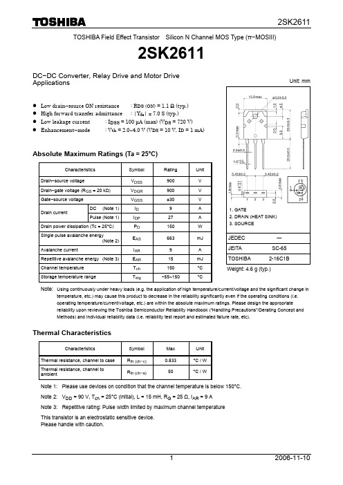
TOSHIBA Field Effect Transistor Silicon N Channel MOS Type (π−MOSIII)2SK2611DC −DC Converter, Relay Drive and Motor Drive Applicationsz Low drain −source ON resistance : R DS (ON) = 1.1 Ω (typ.) z High forward transfer admittance : |Y fs | = 7.0 S (typ.)z Low leakage current : I DSS = 100 μA (max) (V DS = 720 V)z Enhancement −mode : V th = 2.0~4.0 V (V DS = 10 V, I D = 1 mA)Absolute Maximum Ratings (Ta = 25°C)Characteristics Symbol Rating UnitDrain −source voltageV DSS 900 VDrain −gate voltage (R GS = 20 k Ω) V DGR 900 VGate −source voltage V GSS ±30 VDC (Note 1) I D 9 A Drain currentPulse (Note 1)I DP 27A Drain power dissipation (Tc = 25°C)P D 150 WSingle pulse avalanche energy(Note 2) E AS 663mJ Avalanche currentI AR 9 A Repetitive avalanche energy (Note 3) E AR 15 mJChannel temperature T ch 150 °C Storage temperature rangeT stg−55~150 °CNote: Using continuously under heavy loads (e.g. the application of high temperature/current/voltage and the significant change intemperature, etc.) may cause this product to decrease in the reliability significantly even if the operating conditions (i.e. operating temperature/current/voltage, etc.) are within the absolute maximum ratings. Please design the appropriate reliability upon reviewing the Toshiba Semiconductor Reliability Handbook (“Handling Precautions”/Derating Concept and Methods) and individual reliability data (i.e. reliability test report and estimated failure rate, etc).Thermal CharacteristicsCharacteristics Symbol Max UnitThermal resistance, channel to case R th (ch −c) 0.833 °C / W Thermal resistance, channel to ambientR th (ch −a)50°C / WNote 1: Please use devices on condition that the channel temperature is below 150°C. Note 2: V DD = 90 V, T ch = 25°C (initial), L = 15 mH, R G = 25 Ω, I AR = 9 A Note 3: Repetitive rating: Pulse width limited by maximum channel temperature This transistor is an electrostatic sensitive device. Please handle with caution.Unit: mm1. GATE2. DRAIN (HEAT SINK)3. SOURCEJEDEC ―JEITA SC-65 TOSHIBA 2-16C1B Weight: 4.6 g (typ.)Electrical Characteristics (Ta = 25°C)Characteristics SymbolTest ConditionMin Typ. Max Unit Gate leakage currentI GSS V GS = ±30 V, V DS = 0 V — — ±10μA Gate −source breakdown voltage V (BR) GSS I G = ±10 μA, V DS = 0 V ±30 — — V Drain cut −off currentI DSS V DS = 720 V, V GS = 0 V — — 100μA Drain −source breakdown voltage V (BR) DSS I D = 10 mA, V GS = 0 V 900 — — V Gate threshold voltage V th V DS = 10 V, I D = 1 mA 2.0 — 4.0 V Drain −source ON resistance R DS (ON)V GS = 10 V, I D = 4 A— 1.11.4ΩForward transfer admittance |Y fs | V DS = 15 V, I D = 4 A3.07.0 — SInput capacitanceC iss — 2040 —Reverse transfer capacitance C rss — 45 — Output capacitanceC ossV DS = 25 V, V GS = 0 V, f = 1 MHz — 190 —pF Rise timet r — 25 —Turn −on timet on — 60 —Fall timet f — 20 —Switching timeTurn −off timet off— 95 —nsTotal gate charge (gate −sourceplus gate −drain) Q g —58 — Gate −source charge Q gs — 32 — Gate −drain (“miller”) ChargeQ gdV DD ≈ 400 V, V GS = 10 V, I D = 9 A — 26 —nCSource −Drain Ratings and Characteristics (Ta = 25°C)Characteristics SymbolTest ConditionMin Typ. Max UnitContinuous drain reverse current(Note 1)I DR —— — 9 A Pulse drain reverse current(Note 1) I DRP —— — 27 A Forward voltage (diode) V DSF I DR = 9 A, V GS = 0 V——−1.9VReverse recovery time t rr — 1.6 — μs Reverse recovery chargeQ rrI DR = 9 A, V GS = 0 V, dI DR / dt = 100 A / μs— 20 — μCMarkinglead (Pb)-free package or lead (Pb)-free finish.⎟⎠⎞⎜⎝⎛−⋅⋅⋅=DD VDSS VDSS AS V B B I L 21E 2R G = 25 ΩV DD = 90 V , L = 15 mHRESTRICTIONS ON PRODUCT USE20070701-EN •The information contained herein is subject to change without notice.•TOSHIBA is continually working to improve the quality and reliability of its products. Nevertheless, semiconductor devices in general can malfunction or fail due to their inherent electrical sensitivity and vulnerability to physical stress. It is the responsibility of the buyer, when utilizing TOSHIBA products, to comply with the standards of safety in making a safe design for the entire system, and to avoid situations in which a malfunction or failure of such TOSHIBA products could cause loss of human life, bodily injury or damage to property.In developing your designs, please ensure that TOSHIBA products are used within specified operating ranges as set forth in the most recent TOSHIBA products specifications. Also, please keep in mind the precautions and conditions set forth in the “Handling Guide for Semiconductor Devices,” or “TOSHIBA Semiconductor Reliability Handbook” etc.• The TOSHIBA products listed in this document are intended for usage in general electronics applications (computer, personal equipment, office equipment, measuring equipment, industrial robotics, domestic appliances, etc.).These TOSHIBA products are neither intended nor warranted for usage in equipment that requires extraordinarily high quality and/or reliability or a malfunction or failure of which may cause loss of human life or bodily injury (“Unintended Usage”). Unintended Usage include atomic energy control instruments, airplane or spaceship instruments, transportation instruments, traffic signal instruments, combustion control instruments, medical instruments, all types of safety devices, etc.. Unintended Usage of TOSHIBA products listed in his document shall be made at the customer’s own risk.•The products described in this document shall not be used or embedded to any downstream products of which manufacture, use and/or sale are prohibited under any applicable laws and regulations.• The information contained herein is presented only as a guide for the applications of our products. No responsibility is assumed by TOSHIBA for any infringements of patents or other rights of the third parties which may result from its use. No license is granted by implication or otherwise under any patents or other rights of TOSHIBA or the third parties.• Please contact your sales representative for product-by-product details in this document regarding RoHS compatibility. Please use these products in this document in compliance with all applicable laws and regulations that regulate the inclusion or use of controlled substances. Toshiba assumes no liability for damage or losses occurring as a result of noncompliance with applicable laws and regulations.。
SANYO 2SK2617ALS 数据手册
1.0 7 5
3 Operation in this area 2 is limited by RDS(on).
Symbol VDSS VGSS IDc*1 IDpack*2
IDP
PD
Tch Tstg EAS IAV
Conditions
Limited only by maximum temperature SANYO’s ideal heat dissipation condition PW≤10µs, duty cycle≤1% Tc=25°C (SANYO’s ideal heat dissipation condition)
Gate-to-Source Voltage, VGS -- V IT05193
10
yfs -- ID
VDS=10V
7
5
3
2
25°C
Tc=
--25°C 75°C
1.0
7
5
3 2
0.1 0.1
100 7 5
23
5 7 1.0
23
5 7 10
Drain Current, ID -- A
SW Time -- ID
N-Channel Silicon MOSFET
General-Purpose Switching Device Applications
Specifications
Absolute Maximum Ratings at Ta=25°C
Parameter Drain-to-Source Voltage Gate-to-Source Voltage
PW=1µs D.C.≤0.5%
G
ID=2A
RL=100Ω
B261 不锈钢球组气流量调节阀数据规格表说明书

B261•ApplicationStainless Steel Ball and StemTechnical dataFunctional dataValve Size 2.5" [65]Fluidchilled or hot water, up to 60% glycol Fluid Temp Range (water)0...212°F [-18...100°C]Body Pressure Rating 400 psi Close-off pressure ∆ps 100 psiFlow characteristic equal percentage Servicing maintenance-free Flow Pattern 2-way Leakage rate0% for A – AB Controllable flow range 75°Cv60 Body pressure rating note 400 psiCv Flow RatingA-port: as stated in chart B-port: 70% of A – AB Cv MaterialsValve body Nickel-plated brass body Stem seal EPDM (lubricated)SeatPTFEPipe connection NPT female ends O-ring EPDM (lubricated)Ballstainless steel Suitable actuatorsNon-SpringARB(X)Safety notesWARNING: This product can expose you to lead which is known to the State of California to cause cancer and reproductive harm. For more information go to Product featuresThis valve is typically used in air handling units on heating or cooling coils, and fan coil unit heating or cooling coils. Some other common applications include Unit Ventilators, VAV box re-heat coils and bypass loops. This valve is suitable for use in a hydronic system with variable flow.Flow/Mounting detailsB261 DimensionsDimensional drawingsARB, ARXA B C D E F H110.1" [257] 5.6" [141]8.0" [203] 6.0" [152] 2.8" [71] 2.8" [71] 1.9" [48]AFRB, AFRXA B C D E F11.5" [293] 5.6" [141]8.6" [219] 6.6" [168] 2.0" [51] 2.0" [51]ARQB, ARQXA B C D E F H1H29.9" [251] 4.2" [107]8.1" [206] 6.1" [155] 2.3" [58] 2.3" [58]0.8" [20]0.6" [15]AFRB N4, AFRX N4A B D E F11.4" [289] 5.6" [141]8.0" [203] 2.4" [62] 2.4" [62]ARB N4, ARX N4, NRB N4, NRX N4A B D E F11.4" [289] 5.6" [141]8.0" [203] 3.1" [80] 3.1" [80]A B C D E F H1H29.9" [251] 4.2" [107]8.1" [206] 6.1" [155] 2.3" [58] 2.3" [58]0.8" [20]0.6" [15]A B D E F11.4" [289] 5.6" [141]8.0" [203] 3.1" [80] 3.1" [80]AFRBUP-S On/Off, Spring Return, AC 24...240 VTechnical dataElectrical data Nominal voltage AC 24...240 V / DC 24...125 VNominal voltage frequency50/60 HzPower consumption in operation7 WPower consumption in rest position 3.5 WTransformer sizing7 VA @ AC 24 V (class 2 power source), 8.5 VA @AC 120 V, 18 VA @ AC 240 VAuxiliary switch 2 x SPDT, 3 A resistive (0.5 A inductive) @ AC 250 V,one set at 10°, one adjustable 10...90°Switching capacity auxiliary switch 3 A resistive (0.5 A inductive) @ AC 250 VElectrical Connection(2) 18 GA appliance cables with 1/2" conduitconnectors, 3 ft [1 m],Overload Protection electronic throughout 0...95° rotationFunctional data Direction of motion motor selectable by ccw/cw mountingDirection of motion fail-safe reversible with cw/ccw mountingManual override 5 mm hex crank (3/16" Allen), suppliedAngle of rotation90°Running Time (Motor)75 sRunning time fail-safe<20 sNoise level, motor45 dB(A)Noise level, fail-safe62 dB(A)Position indication MechanicalSafety data Degree of protection IEC/EN IP54Degree of protection NEMA/UL NEMA 2 UL Enclosure Type 2Agency Listing cULus acc. to UL60730-1A/-2-14, CAN/CSAE60730-1:02, CE acc. to 2014/30/EU and 2014/35/EU; Listed to UL 2043 - suitable for use in airplenums per Section 300.22(c) of the NEC andSection 602.2 of the IMCQuality Standard ISO 9001Ambient temperature-22...122°F [-30...50°C]Storage temperature-40...176°F [-40...80°C]Ambient humidity max. 95% r.H., non-condensingServicing maintenance-freeWeight Weight 5.7 lb [2.6 kg]Electrical installationINSTALLATION NOTESActuators with appliance cables are numbered.AFRBUP-SUniversal Power Supply (UP) models can be supplied with 24 VAC up to 240 VAC, or 24 VDC up to 125 VDC.Provide overload protection and disconnect as required.Two built-in auxiliary switches (2x SPDT), for end position indication, interlock control, fan startup, etc.Actuators may be powered in parallel. Power consumption must be observed.Parallel wiring required for piggy-back applications.Meets cULus requirements without the need of an electrical ground connection.Warning! Live Electrical Components!During installation, testing, servicing and troubleshooting of this product, it may be necessary to workwith live electrical components. Have a qualified licensed electrician or other individual who has beenproperly trained in handling live electrical components perform these tasks. Failure to follow all electricalsafety precautions when exposed to live electrical components could result in death or serious injury.Apply only AC line voltage or only UL-Class 2 voltage to the terminals of auxiliary switches. Mixed orcombined operation of line voltage/safety extra low voltage is not allowed.On/Off Auxiliary Switches。
sa-268
SPECIFICATION FOR SEAMLESS AND WELDED FERRITIC AND MARTENSITIC STAINLESS STEEL TUBING FOR GENERAL SERVICESA-268/SA-268M(Identical with ASTM Specification A268/A268M-94.)1.Scope1.1.This specification covers a number of grades ofnominal-wall-thickness,stainless steel tubing for generalcorrosion-resisting and high-temperature service.Mostof these grades are commonly known as the“straight-chromium”types and are characterized by being ferro-magnetic.Two of these grades,TP410and UNS S41500(Table1),are amenable to hardening by heat treatment,and the high-chromium,ferritic alloys are sensitive tonotch-brittleness on slow cooling to ordinary tempera-tures.These features should be recognized in the useof these materials.Grade TP439is used primarily forhot-water tank service and does not require post-weldheat treatment to prevent attack of the heat affected zone.NOTE1—TP329(S32900)formerly in this specification,has beentransferred to A789/A789M and A790/A790M.1.2An optional supplementary requirement is pro-vided,and when desired,shall be so stated in the order.NOTE2—For tubing smaller than1⁄2in.[12.7mm]in outsidediameter,the elongation values given for strip specimens in Table2shall apply.Mechanical property requirements do not apply totubing smaller than1⁄8in.[3.2mm]in outside diameter or withwalls thinner than0.015in.[0.4mm].1.3The values stated in either inch-pound units orSI units are to be regarded separately as standard.Within the text,the SI units are shown in brackets.Thevalues stated in each system are not exact equivalents;therefore,each system must be used independently ofthe bining values from the two systems mayresult in nonconformance with the specification.Theinch-pound units shall apply unless the“M”designationof this specification is specified in the order.4232.Referenced Documents2.1ASTM Standards:A450/A450M Specification for General Requirementsfor Carbon,Ferritic Alloy,and Austenitic Alloy SteelTubesA480/A480M Specification for General Requirementsfor Flat-Rolled Stainless and Heat-Resisting SteelPlate,Sheet,and StripA763Practices for Detecting Susceptibility to Intergran-ular Attack in Ferritic Stainless SteelsA789/A789M Specification for Seamless and WeldedFerritic/Austenitic Stainless Steel Tubing for GeneralServiceA790/A790M Specification for Seamless and WeldedFerritic/Austenitic Stainless Steel PipeE527Practice for Numbering Metals and Alloys(UNS)2.2Other Standard:SAE J1086Practice for Numbering Metals and Alloys(UNS)3.General Requirements3.1Material furnished under this specification shallconform to the applicable requirements of SpecificationA450/A450M unless otherwise provided herein.4.Ordering Information4.1Orders for material under this specification shouldinclude the following,as required,to described thedesired material adequately:SA-268/SA-268M1998SECTION II4.1.1Quantity(feet,metres,or number of lengths),4.1.2Name of material(seamless or welded tubes),4.1.3Grade(Table1),4.1.4Size(outside diameter and nominal wall thickness),4.1.5Length(specific or random),4.1.6Optional requirements(hydrostatic or electric test,13.7),4.1.7Test report required(Certification Section of Specification A450/A450M),4.1.8Specification designation,and4.1.9Special requirements.5.Manufacture5.1The tubes shall be made by the seamless or welded process with nofiller metal added.6.Heat Treatment6.1As afinal heat treatment,tubes shall be reheatedto a temperature of1200°F[650°C]or higher and cooled(as appropriate for the grade)to meet the requirements of this specification.6.2The martensitic grade UNS S41500shall be reheated to a temperature of950°F[510°C]or higher and cooled as appropriate to meet the requirements of this specification.7.Chemical Composition7.1The steel shall conform to the chemical require-ments prescribed in Table1.8.Product Analysis8.1An analysis of either one billet or one lengthofflat-rolled stock or one tube shall be made from each heat.The chemical composition thus determined shall conform to the requirements specified.8.2The product analysis tolerance of the Chemical Requirements Table of A480/A480M shall apply. The product analysis tolerance is not applicable to the carbon content for material with a specified maximum carbon of0.04%or less.4248.3If the original test for product analysis fails, retests of two additional billets,lengths offlat-rolled stock or tubes shall be made.Both retests for the elements in question shall meet the requirements of the specification;otherwise all remaining material in the heat or lot(Note3)shall be rejected or,at the option of the producer,each billet or tube may be individually tested for acceptance.Billets,lengths of flat-rolled stock or tubes which do not meet the require-ments of the specification shall be rejected.NOTE3—Forflange andflaring requirements,the term lot applies to all tubes prior to cutting of the same nominal size and wall thickness which are produced from the same heat of steel.When final heat treatment is in batch-type furnace,a lot shall include only those tubes of the same size and from the same heat which are heat treated in the same furnace charge.When thefinal heat treatment is in a continuous furnace,the number of tubes of the same size and from the same heat in a lot shall be determined from the size of the tubes as prescribed in Table2.NOTE4—For tensile and hardness test requirements,the term lot applies to all tubes prior to cutting,of the same nominal diameter and wall thickness that are produced from the same heat of steel. Whenfinal heat treatment is in a batch-type furnace,a lot shall include only those tubes of the same size and the same heat which are heat treated in the same furnace charge.When thefinal heat treatment is in a continuous furnace,a lot shall include all tubes of the same size and heat,heat treated in the same furnace at the same temperature,time at heat,and furnace speed.9.Tensile Requirements9.1The material shall conform to the tensile proper-ties prescribed in Table3.10.Hardness Requirements10.1The tubes shall have a hardness number not to exceed those prescribed in Table4.11.Permissible Variations in Dimensions11.1Variations in outside diameter,wall thickness, and length from those specified shall not exceed the amounts prescribed in Table5.11.2The permissible variations in outside diameter given in Table5are not sufficient to provide for ovality in thin-walled tubes,as defined in the Table.In such tubes,the maximum and minimum diameters at any cross section shall deviate from the nominal diameter by no more than twice the permissible variation in outside diameter given in Table5;however,the mean diameter at that cross section must still be within the given permissible variation.PART A—FERROUS MATERIAL SPECIFICATIONS SA-268/SA-268M12.Surface Condition12.1All tubes shall be free of excessive mill scale, suitable for inspection.A slight amount of oxidationwill not be considered as scale.Any specialfinish requirements shall be subject to agreement between the manufacturer and the purchaser.13.Mechanical Tests Required13.1Tension Tests—One tension test shall be madeon a specimen for lots of not more than50tubes. Tension tests shall be made on specimens from two tubes for lots of more than50tubes(Note4).13.2Flaring Test(For Seamless Tubes)—One test shall be made on specimens from one end of one tube from each lot(Note3)offinished tubes.The minimum expansion of the inside diameter shall be10%.For tubes over8in.[203.2mm]in outside diameter,or tubes with wall thickness3⁄8in.[9.52mm]and over,theflattening test may be performed instead of theflaring test unless theflaring test is specified in the purchase order.13.3Flange Test(For Welded Tubes)—One test shall be made on specimens from one end of one tube from each lot(Note3)offinished tubes.For tubes over8in.[203.2mm]in outside diameter,or tubes with wall thickness3⁄8in.[9.52mm]and over,the425flattening test may be performed instead of theflange test unless theflange test is specified in the purchase order.13.4Hardness Test—Brinell or Rockwell hardness tests shall be made on specimens from two tubes from each lot(Note4).13.5When more than one heat is involved,the tension,flaring,flanging,and hardness test requirements shall apply to each heat.13.6Reverse Flattening Test—For welded tubes, one reverseflattening test shall be made on a specimen from each1500ft[450m]offinished tubing.13.7Hydrostatic or Nondestructive Electric Test—Each welded tube shall be subjected to either the hydrostatic or nondestructive electric test.The purchaser may specify which test is to be used.Each seamless tube shall be subjected to the hydrostatic test,or,instead of this test,a nondestructive electric test may be used when specified by the purchaser.14.Product Marking14.1In addition to the marking described in Specifi-cation A450/A450M,the marking shall indicate whether the tubing is seamless or welded.15.Keywords15.1ferritic stainless steel;seamless steel tube;stain-less steel tube;steel tube;welded steel tubeSA-268/SA-268M1998SECTION IITABLE1CHEMICAL REQUIREMENTSNOTE—TP329(S32900),formerly part of this specification,has been transferred to A789/A789M and A790/A790M.Grade TP405TP410TP429TP430TP443TP446-1TP446-2A...TP409 UNSDesignation B S40500S41000S42900S43000S44300S44600S44600S40800S40900 Element Composition,%C,max0.080.150.120.120.200.200.120.080.08Mn,max 1.00 1.00 1.00 1.00 1.00 1.50 1.50 1.00 1.00P,max0.0400.0400.0400.0400.0400.0400.0400.0450.045S,max0.0300.0300.0300.0300.0300.0300.0300.0450.045Si,max0.750.750.750.750.750.750.75 1.00 1.00Ni0.50max0.50max0.50max0.50max0.50max0.50max0.50max0.80max0.50maxCr11.5–13.511.5–13.514.0–16.016.0–18.018.0–23.023.0–30.023.0–30.011.5–13.010.50–11.75 Mo...........................Al0.10–0.30........................ Cu............0.90–1.25............ N...............0.10–0.250.10–0.25...... Ti.....................12×C min;6×C min;1.10max0.75maxTP TPGrade TP439...TP430Ti XM-27XM-33D18Cr-2Mo29-429-4-226-3-325-4-4...C...UNSDesignation S43035S41500E S43036S44627S44626S44400S44700S44800S44660S44635S44735S32803 Element Composition,%C,max0.070.050.100.01D0.060.0250.0100.0100.0300.0250.0300.015H Mn,max 1.000.5–1.0 1.000.400.75 1.000.300.30 1.00 1.00 1.000.5P,max0.0400.030.0400.020.0400.0400.0250.0250.0400.0400.0400.020S,max0.0300.030.0300.020.0200.0300.0200.0200.0300.0300.0300.005Si,max 1.000.60 1.000.400.75 1.000.200.20 1.000.75 1.000.50Ni0.50max 3.5–5.50.75max0.5F max0.50max 1.00max0.15max 2.0–2.5 1.0–3.50 3.5–4.5 1.00max 3.0–4.0Cr17.00–11.5–14.016.00–25.0–27.525.0–27.017.5–19.528.0–30.028.0–30.025.0–28.024.5–26.028.00–28.0–29.019.0019.5030.00Mo...0.5–1.0...0.75–1.500.75–1.50 1.75–2.50 3.5–4.2 3.5–4.2 3.0–4.0 3.5–4.5 3.60–4.20 1.8–2.5Al,max0.15.................................Cu,max.........0.20.20...0.150.15............N,max0.04......0.0150.0400.0350.020G0.020G0.0400.0350.0450.020Ti0.20+4(C...5×C min;...7×(C+N)(Ti+Cb)......(Ti+Cb)p(Ti+Cb)p(Ti+Cb)...+N)min;0.75but no less0.20+40.20–1.000.20+40.201.001.10max max than0.20(C+N)and6×(C+N)with6(Cmin;1.00min;0.80C+N)min to+N)minmax max min0.80maxCb.........0.05–0.20.....................0.15–0.50IA TP446-2is a lower carbon version of TP446-1that has a lower tensile strength but improved ductility and fracture toughness.B New designation established in accordance with Practice E527and SAE J1086,Practice for Numbering Metals and Alloys(UNS).C When intergranular corrosion testing is specified,the test will be Practices A763,using samples prepared as agreed upon between the seller and the purchaser.D For small diameter or thin walls,or both,tubing,where many drawing passes are required,a carbon maximum of0.015%is necessary.Small outside diameter tubes aredefined as those less than0.500in.[12.7mm]in outside diameter and light wall tubes as those less than0.049in.[1.2mm]in average wall thickness(0.040in.[1mm] in minimum wall thickness).E Plate version of CA6NM.F Nickel plus copper.G Carbon plus nitrogen p0.025%max.H Carbon plus nitrogen p0.30max.I Cb/(C+N)p12min.426PART A—FERROUS MATERIAL SPECIFICATIONS SA-268/SA-268MTABLE2NUMBER OF TUBES IN A LOT HEAT TREATED BY THE CONTINUOUS PROCESSSize of Tube Size of Lot2in.[50.8mm]and over in outside diameter and0.200in.[5.1mm]not more than50tubesand over in wall thicknessLess than2in.[50.8mm]but over1in.[25.4mm]in outside diameter not more than75tubesor over1in.[25.4mm]in outside diameter and under0.200in.[5.1mm]in wall thickness1in.[25.4mm]or less in outside diameter not more than125tubesTABLE3TENSILE REQUIREMENTSNOTE—TP329(S32900),formerly part of this specification,has been transferred to A789/A789M andA790/A790M.Tensile Yieldstrength,strength,Elongation Amin,min,in2in.or50 Grade and UNS Designation ksi[MPa]ksi[MPa]mm,min,%TP40560[415]30[205]20S40500...55[380]30[205]20S40800TP41060[415]30[215]20S41000TP429,TP430,and TP430Ti60[415]35[240]20S429000,S43000,and S43036TP44370[485]40[275]20S44300TP446-170[485]40[275]18S44600TP446-265[450]40[275]20S44600TP40955[380]30[205]20S40900TP43960[415]30[205]20S43035...115[795]90[620]15S41500TPXM-2765[450]40[275]20S44627TPXM-3368[470]45[310]20S4462618Cr-2Mo60[415]40[275]20S4440029-4and29-4-280[550]60[415]20S44700and S4480026-3-385[585]65[450]20S4466025-4-490[620]75[515]20S44635...75[515]60[415]18S4473528-2-3.587[600]72[500]16S32803427SA-268/SA-268M1998SECTION IITABLE3(CONT’D)TENSILE REQUIREMENTSElongation in2in.Wall Thickness or50mm,min,%TP446-1and All Other in.mm S44735S41500Grades5⁄16[0.312]81815209⁄32[0.281]7.21714191⁄4[0.250] 6.41614187⁄32[0.219] 5.61513173⁄16[0.188] 4.81412165⁄32[0.156]41311151⁄8[0.125] 3.21311143⁄32[0.094] 2.41210131⁄16[0.062] 1.611912 0.062–0.035,excl 1.6–0.910812 0.035–0.022,excl0.9–0.610811 0.022–0.015,incl0.6–0.410811 NOTES—The above table gives the computed minimum values for each1⁄32in.[0.8mm]decrease in wall thickness.Where the wall thickness lies between two values shown above,the minimum elongation value shall be determined by the following equation:Grade EquationTP446-1and S44735E p28.8t+9.00[E p1.13t+9.00]S41500E p24t+7.5All other grades E p32t+10.00[E p1.25t+10.00]where:E p Elongation in2in.or50mm,%,andt p actual thickness of specimen,in.[mm].A For longitudinal strip tests a deduction of0.90%for TP446-1and S44735and1.00%for all other grades shall be made from the basic minimum elongation for each1⁄32in.[0.8mm]decrease in wall thickness below5⁄16in.[8mm].The following table gives the computed minimum values.B Calculated elongation requirements shall be rounded to the nearest whole number.428PART A—FERROUS MATERIAL SPECIFICATIONS SA-268/SA-268MTABLE4HARDNESS REQUIREMENTSNOTE—TP329(S32900),formerly part of this specification,has been transferred to A789/A789Mand A790/A790M.Brinell RockwellHardness,Hardness,Grade UNS Designation max B Scale,maxTP405S4050020795...S4080020795TP410S4100020795TP429,TP430,and S42900,S43000,19090TP430Tl and S43036TP443S4430020795TP446-1and S4460020795TP446-2TP409S4090020795TP439S4305519090...S4*******A32TPXM-33and S44626and241100TPXM-27S4462718Cr-2Mo S444002179529-4and29-4-2S44700and207100S4480026-3-3S4466026525A25-4-4S4463527027A...S44735 (100)28-2-3.5S32803240100A Rockwell hardness,C scale.TABLE5PERMISSIBLE VARIATIONS IN DIMENSIONSPermissible Variations inCutSize,Outside Permissible Variations Permissible Length,in.A[mm]Diameter,in.in Outside Diameter,Variations in WallGroup[mm]in.[mm]Thickness,%C Over Under Thin Walled Tubes B1Up to1⁄2[12.7],exclϮ0.005[0.13]Ϯ151⁄8[3]0...21⁄2to11⁄2[12.7to38.1],exclϮ0.005[0.13]Ϯ101⁄8[3]0less than0.065in.[1.6mm]nominal311⁄2to31⁄2[38.1to88.9],Ϯ0.010[0.25]Ϯ103⁄16[5]0less than0.095in.[2.4mm] excl nominal431⁄2to51⁄2[88.9to139.7],Ϯ0.015[0.38]Ϯ103⁄16[5]0less than0.150in.[3.8mm] excl nominal551⁄2to8[139.7to203.2],Ϯ0.030[0.76]Ϯ103⁄16[5]0less than0.150in.[3.8mm] incl nominalA These tolerances apply to cut lengths up to and including24ft[7.3m].For lengths greater than24ft[7.3m],the above over tolerances shall be increased by1⁄8in.[3mm]for each10ft[3m]or fraction thereof over24ft,or1⁄2in.[13mm],whichever is lesser.B Ovality provisions of12.2apply.C When tubes as ordered require wall thicknesses3⁄4in.[19mm]or over,or an inside diameter60%or less of the outside diameter,a widervariation in wall thickness is required.On such sizes a variation in wall thickness of12.5%over or under will be permitted.For tubes less than1⁄2in.[12.7mm]in inside diameter which cannot be successfully drawn over a mandrel,the wall thickness may vary Ϯ15%from that specified.429SA-268/SA-268M1998SECTION IISUPPLEMENTARY REQUIREMENTSThe following supplementary requirement shall apply only when specified by thepurchaser in the inquiry,contract,or order.S1.Air-Underwater Pressure TestS1.1Each tube,with internal surface clean and dry,shall be internally pressurized to150psi[1000kPa]minimum with clean and dry compressed air whilebeing submerged in clear water.S1.2The tube shall be well-lighted,preferably byunderwater illumination.S1.3Any evidence of air leakage of the pneumaticcouplings shall be corrected prior to testing.S1.4After holding the pressure for not less than5s after the surface of the water has become calm,aninspection shall be made of the entire external surfaceof the tube.S1.5If any tube leaks during the air-underwater test,it shall be rejected.Any leaking areas may be cut outand the tube retested as above.430。
- 1、下载文档前请自行甄别文档内容的完整性,平台不提供额外的编辑、内容补充、找答案等附加服务。
- 2、"仅部分预览"的文档,不可在线预览部分如存在完整性等问题,可反馈申请退款(可完整预览的文档不适用该条件!)。
- 3、如文档侵犯您的权益,请联系客服反馈,我们会尽快为您处理(人工客服工作时间:9:00-18:30)。
1
)Max. temperature of the terminals T T = 100/C – Max. Temperatur der Anschlüsse T T = 100/C 1
03.06.2003
Fast Switching
Schnelle Si-Gleichrichter Surface Mount Si-Rectifiers
für die Oberflächenmontage
Nominal current – Nennstrom 2 A
Repetitive peak reverse voltage 1200…1800 V Periodische Spitzensperrspannung Plastic case MELF
DO-213AB
Kunststoffgehäuse MELF Weight approx. – Gewicht ca.
0.12 g
Plastic material has UL classification 94V-0Gehäusematerial UL94V-0 klassifiziert
Dimensions / Maße in mm
Standard packaging taped and reeled see page 18Standard Lieferform gegurtet auf Rolle siehe Seite 18
Maximum ratings Grenzwerte
Type Typ Repetitive peak reverse voltage Periodische Spitzensperrspannung
V RRM [V]
Surge peak reverse voltage Stoßspitzensperrspannung
V RSM [V]
SA 26112001200SA 26214001400SA 26316001600SA 264
1800
1800
Max. average forward rectified current, R-load T T = 100/C I FAV 2 A Dauergrenzstrom in Einwegschaltung mit R-Last Repetitive peak forward current f > 15 Hz I FRM 10 A 1)Periodischer Spitzenstrom
Peak forward surge current, 50 Hz half sine-wave T A = 25/C I FSM 50 A Stoßstrom für eine 50 Hz Sinus-Halbwelle Rating for fusing – Grenzlastintegral, t < 10 ms T A = 25/C
i 2t 12.5 A 2s Operating junction temperature – Sperrschichttemperatur T j – 50...+175/C Storage temperature – Lagerungstemperatur
T S
– 50...+175/C
1
)Valid, if mounted on P.C. board with 25 mm 2 copper pads at each terminal
Dieser Wert gilt bei Montage auf Leiterplatte mit 25 mm 2 Kupferbelag (Lötpad) an jedem Anschluß
2
Characteristics
Kennwerte
Forward voltage – Durchlaßspannung T j = 25/C I F = 2 A V F < 1.8 V Leakage current – Sperrstrom T j = 25/C V R = V RRM I R < 5 :A T j = 100/C
V R = V RRM
I R < 100 :A Reverse recovery time I F = 0.5 A through/über t rr < 500 ns Sperrverzug
I R = 1 A to/auf I R = 0.25 A
Thermal resistance junction to ambient air
R thA < 40 K/W 1)Wärmewiderstand Sperrschicht – umgebende Luft Thermal resistance junction to terminal
R thT
< 15 K/W
Wärmewiderstand Sperrschicht – Kontaktfläche。