4014面板光学报告
干法刻蚀制程工艺及相关缺陷的分析和改善

and RF homogeneity. Meanwhile, accelerating the production beat has most significant impact on the first two factors. Experiment on SVA-NEC 5Generation factory's process equipment to obtain data for mapping into the trends, identify the most dry etching good conditions from variety ways. This paper focus on the Dry-etching process defect analysis and tracking to identify the relevant measures to solve the practical problems encountered in production.
申请上海交通大学工程硕士专业学位论文
干法刻蚀制程工艺及相关缺陷的分析和改善
学 校:上海交通大学 院 系:电子信息与电子工程学院 工程硕士生:张新言 工程领域:平板显示 导 师Ⅰ:李荣玉(副教授) 导 师Ⅱ:陈勤达(高级工程师)
上海交通大学电子信息与电气工程学院 2009 年 9 月
A Dissertation Submitted to Shanghai Jiao Tong University for Master Degree of Engineering
Experimental results and conclusions of this paper has been in the dry etching process was applied.
B101EW04 V0 spec_10.1寸AU屏

1 of 31B101EW03 V0 document version : 0.1( ) Preliminary Specifications (V ) Final SpecificationsModule 10.1” SD+ 16:10 TFT-LCD Model Name B101EW04 V0Note ()LED Backlight without driving circuit designCustomerDateNormal 02/15/2011Checked & Approved byDate Note: This Specification is subject to change without notice.Approved by DateIvan Wu02/15/2011Prepared byJay Lin 02/15/2011NBBU Marketing Division / AU Optronics corporation2 of 31B101EW03 V0 document version : 0.1 Contents1. Handling Precautions........................................................................................................4 2. General Description . (5)2.1 General Specification......................................................................................................................................5 2.2 Optical Characteristics...................................................................................................................................6 3. Functional Block Diagram ...............................................................................................11 The following diagram shows the functional block of the 10.1 inches wide Color TFT/LCD 40 Pin (One ch/connector Module).....................................................................................11 4. Absolute Maximum Ratings (12)4.1 Absolute Ratings of TFT LCD Module.........................................................................................................12 4.2 Absolute Ratings of Environment................................................................................................................12 5. Electrical characteristics. (13)5.1 TFT LCD Module............................................................................................................................................13 5.2 Backlight Unit ................................................................................................................................................15 6. Signal Characteristic. (16)6.1 Pixel Format Image........................................................................................................................................16 6.2 The input data format....................................................................................................................................17 6.3 Integration Interface Requirement...............................................................................................................18 6.4 Interface Timing.............................................................................................................................................20 6.5 Power Sequence............................................................................................................................................21 6.5.1 Panel Power Sequence..............................................................................................................................21 7. Panel Reliability Test (22)7.1 Vibration Test.................................................................................................................................................22 7.2 Shock Test......................................................................................................................................................22 7.3 Reliability Test ...............................................................................................................................................22 8. Mechanical Characteristics. (23)8.1 LCM Outline Dimension................................................................................................................................23 9. Shipping and Package.. (25)9.1 Shipping Label Format..................................................................................................................................25 9.2 Carton Package .............................................................................................................................................26 9.3 Shipping package of palletizing sequence.................................................................................................27 10. Appendix . (28)10.1 EDID description (28)3 of 31B101EW03 V0 document version : 0.1Record of RevisionVersion and Date Page Old descriptionNew DescriptionRemark 0.1 2010/10/28 All First Edition for Customer4 of 31B101EW03 V0 document version : 0.11. Handling Precautions1) Since front polarizer is easily damaged, pay attention not to scratch it.2) Be sure to turn off power supply when inserting or disconnecting from input connector. 3) Wipe off water drop immediately. Long contact with water may cause discoloration or spots.4) When the panel surface is soiled, wipe it with absorbent cotton or other soft cloth.5) Since the panel is made of glass, it may break or crack if dropped or bumped on hard surface.6) Since CMOS LSI is used in this module, take care of static electricity and insure human earth when handling.7) Do not open nor modify the Module Assembly.8) Do not press the reflector sheet at the back of the module to any directions.9) At the insertion or removal of the Signal Interface Connector, be sure not to rotate nor tilt the Interface Connector of the TFT Module.11) After installation of the TFT Module into an enclosure (Notebook PC Bezel, for example), do not twist nor bend the TFT Module even momentary. At designing the enclosure, it should be taken into consideration that no bending/twisting forces are applied to the TFT Module from outside. Otherwise the TFT Module may be damaged. 12) S mall amount of materials having no flammability grade is used in the LCD module. The LCD module should be supplied by power complied with requirements of Limited Power Source (IEC60950 or UL1950), or be applied exemption. 13) D isconnecting power supply before handling LCD modules, it can prevent electric shock, DO NOT TOUCH the electrode parts, cables, connectors and LED circuit part of TFT module that a LED light bar build in as a light source of back light unit. It can prevent electrostatic breakdown.5 of 31B101EW03 V0 document version : 0.12. General DescriptionB101EW03 V0 is a Color Active Matrix Liquid Crystal Display composed of a TFT LCD panel, a driver circuit, and LED backlight system. The screen format is intended to support 1280(H) x 800(V) screen and 262k colors (RGB 6-bits data driver) with LED backlight driving circuit. All input signals are LVDS interface compatible.B101EW03 V0 is designed for a display unit of notebook style personal computer and industrial machine.2.1 General SpecificationThe following items are characteristics summary on the table at 25 ℃ condition:ItemsUnit SpecificationsScreen Diagonal [mm] 255.85(10.07W”) Active Area [mm] 216.96(H) x 135.6(V) Pixels H x V 1280x3(RGB) x 800 Pixel Pitch [mm] 0.1695(H) x 0.1695(V) Pixel Arrangement R.G.B. Vertical Stripe Display ModeNormally BlackWhite LuminanceNote: I LED is LED current [cd/m 2] 400 typ, 320minLuminance Uniformity (5P) 1.25 max Contrast Ratio 600 min Response Time[ms] 25 typ Nominal Input Voltage VDD [Volt] +3.3 typ.Power Consumption[Watt]Typ Max - 3.1W @ Black patternWeight[Grams] 190g max. Physical Size[mm] LWT Max 229.96 149.6 5.56 Typical 229.46 149.1 Min 228.96 148.6 3.39Electrical Interface 1 channel LVDS6 of 31B101EW03 V0 document version : 0.1 Glass Thickness [mm] 0.3 Surface Treatment GlareSupport Color262K colors ( RGB 6-bit +FRC)Temperature Range OperatingStorage (Non-Operating) [oC] [o C]0 to +50 -20 to +60RoHS ComplianceRoHS Compliance2.2 Optical CharacteristicsThe optical characteristics are measured under stable conditions at 25℃ (Room Temperature) :ItemSymbolConditions Min. Typ. Max. Unit NoteWhite LuminanceILED=18.5mA5 points average320 400 - cd/m 21, 4, 5θR θL Horizontal (Right) CR = 10 (Left) 80 80 - - - - degreeViewing AngleψH ψL Vertical (Upper) CR = 10 (Lower)80 80 - - - - 4, 9Luminance Uniformity δ5P 5 Points - - 1.25 1, 3, 4 Luminance Uniformity δ13P 13 Points- - 1.60 2, 3, 4 Contrast Ratio CR 600 - - 4, 6 Cross talk % 4 4, 7T r Rising - - - T f Falling - - - Response TimeT RTRising + Falling-25-msec4, 8Rx 0.542 0.582 0.622 RedRy 0.303 0.343 0.383 Gx 0.294 0.334 0.374 Green Gy 0.540 0.580 0.620Bx 0.107 0.147 0.187 Blue By 0.089 0.129 0.169 Wx 0.273 0.313 0.353 Color / Chromaticity CoodinatesWhiteWy 0.289 0.329 0.369 NTSC%CIE 1931-45-47 of 31B101EW03 V0 document version : 0.1Note 1: 5 points position (Ref: Active area)Note 2: 13 points position (Ref: Active area)Note 3: The luminance uniformity of 5 or13 points is defined by dividing the maximum luminance values by the minimum test point luminanceδW13 = Maximum Brightness of thirteen pointsMinimum Brightness of thirteen points Maximum Brightness of five pointsδW5 = Minimum Brightness of five points8 of 31B101EW03 V0 document version : 0.1Note 4: Measurement methodThe LCD module should be stabilized at given temperature for 30 minutes to avoid abrupt temperature change during measuring. In order to stabilize the luminance, the measurement should be executed after lighting Backlight for 30 minutes in a stable, windless and dark room, and it should be measured in the center of screen.Note 5: Definition of Average Luminance of White (Y L ):Measure the luminance of gray level 63 at 5 points ,Y L = [L (1)+ L (2)+ L (3)+ L (4)+ L (5)] / 5 L (x) is corresponding to the luminance of the point X at Figure in Note (1).Note 6: Definition of contrast ratio:Contrast ratio is calculated with the following formula.Contrast ratio (CR)=Brightness on the “White” state Brightness on the “Black” state9 of 31B101EW03 V0 document version : 0.1 Note 7: Definition of Cross Talk (CT)CT = | Y B – Y A | / Y A × 100 (%) WhereY A = Luminance of measured location without gray level 0 pattern (cd/m 2) Y B = Luminance of measured location with gray level 0 pattern (cd/m 2)Note 8: Definition of response time:The output signals of BM-7 or equivalent are measured when the input signals are changed from “Black” to “White” (falling time) and from “White” to “Black” (rising time), respectively. The response time interval between the10% and 90% of amplitudes. Refer to figure as below.10 of 31B101EW03 V0 document version : 0.1Note 9. Definition of viewing angleViewing angle is the measurement of contrast ratio ≧10, at the screen center, over a 180° horizontal and180° vertical range (off-normal viewing angles). The 180° viewing angle range is broken down as follows; 90° (θ) horizontal left and right and 90° (Φ) vertical, high (up) and low (down). The measurement direction is typically perpendicular to the display surface with the screen rotated about its center to develop the desired measurement viewing angle.11 of 31B101EW03 V0 document version : 0.1 3. Functional Block DiagramThe following diagram shows the functional block of the 10.1 inches wide Color TFT/LCD 40 Pin (One ch/connector Module). TBD12 of 31B101EW03 V0 document version : 0.1 4. Absolute Maximum RatingsAn absolute maximum rating of the module is as following:4.1 Absolute Ratings of TFT LCD ModuleItemSymbol Min Max Unit Conditions Logic/LCD Drive VoltageVin-0.3+4.0[Volt]Note 1,213 of 31B101EW03 V0 document version : 0.1 5. Electrical characteristics 5.1 TFT LCD Module5.1.1 Power SpecificationInput power specifications are as follows;SymbleParameterMinTypMaxUnit sNoteVDD Logic/LCD Drive Voltage 3.0 3.3 3.6 [Volt]PDD VDD Power - -1.0[Watt ]Note 1/2 IDD IDD Current - 257.6 303.03 [mA]Note 1/2 IRush Inrush Current - -1500 [mA] Note 3VDDrpAllowableLogic/LCD Drive Ripple Voltage--100[mV] p-pNote 1 : Maximum Measurement Condition :Black Pattern Note 2:Typical Measurement Condition: Mosaic Pattern Note 3:Measure ConditionVin rising time0V3.3V14 of 31B101EW01 V2 document version : 2.1 5.1.2 Signal Electrical CharacteristicsInput signals shall be low or High-impedance state when VDD is off.It is recommended to refer the specifications of SN75LVDS82DGG (Texas Instruments) in detail.Signal electrical characteristics are as follows;Parameter ConditionMin MaxUnit V th Differential Input High Threshold (Vcm=+1.2V) 100[mV] V tl Differential Input Low Threshold (Vcm=+1.2V) -100 -[mV] V ID Differential Input Voltage100 600 [mV] V cmDifferential InputCommon Mode Voltage1.1251.375[V]Note: LVDS Signal Waveform15 of 31B101EW01 V2 document version : 2.1 5.2 Backlight Unit5.2.1 LED characteristicsParameter Symbol Min Typ Max Units Condition- - 2.1 [Watt] (Ta=25℃), Note 1Type I , V in =12VBacklight Power ConsumptionPLEDLED Life-Time N/A 12,000--Hour (Ta=25℃), Note 2I F =18.5 mANote 1: Calculator value for reference P LED = V F (Normal Distribution) * I F (Normal Distribution) / Efficiency Note 2: The LED life-time define as the estimated time to 50% degradation of initial luminousNote 3: This panel will support lower duty ratio at PWM conditional frequency. The PWM frequency constrainbetween 100 Hz to 300 Hz and a same typical 200Hz. The duty ratio support from 5% to 100%.5.2.2 Backlight input signal characteristicsParameter Symbol Min Typ Max Units Remark6.0 12.0 21.0 [Volt] Type I, Note 1LED Power Supply VLED 4.5 5 5.5 [Volt] Type II, Note 1LED Enable Input High Level 2.5 - 5.5 [Volt] LED Enable Input Low LevelVLED_EN- - 0.8 [Volt] PWM Logic Input High Level2.5 - 5.5 [Volt] PWM Logic Input Low LevelVPWM_EN-- 0.8 [Volt] PWM Input Frequency FPWM 100 - 1K HzPWM Duty Ratio Duty 1 -- 100 % PWM Frequency <5K HzPWM Duty RatioDuty15--100%PWM Frequency ≧500 HzNote 1: Type I and II is an independent of design parameter. It should be separated from system design.6. Signal Characteristic6.1 Pixel Format ImageFollowing figure shows the relationship of the input signals and LCD pixel format.6.2 The input data formatSignal Name DescriptionR5 R4 R3 R2 R1 R0 Red Data 5 (MSB)Red Data 4Red Data 3Red Data 2Red Data 1Red Data 0 (LSB)Red-pixel DataRed-pixel DataEach red pixel's brightness data consists ofthese 6 bits pixel data.G5 G4 G3 G2 G1 G0 Green Data 5 (MSB)Green Data 4Green Data 3Green Data 2Green Data 1Green Data 0 (LSB)Green-pixel DataGreen-pixel DataEach green pixel's brightness data consists ofthese 6 bits pixel data.B5 B4 B3 B2 B1 B0 Blue Data 5 (MSB)Blue Data 4Blue Data 3Blue Data 2Blue Data 1Blue Data 0 (LSB)Blue-pixel DataBlue-pixel DataEach blue pixel's brightness data consists ofthese 6 bits pixel data.RxCLKIN Data Clock The typical frequency is 54.2MHZ.The signal isused to strobe the pixel data and DE signals. Allpixel data shall be valid at the falling edge whenthe DE signal is high.DE Display Timing This signal is strobed at the falling edge ofRxCLKIN. When the signal is high, the pixeldata shall be valid to be displayed.VS Vertical Sync The signal is synchronized to RxCLKIN .HS Horizontal Sync The signal is synchronized to RxCLKIN .Note: Output signals from any system shall be low or High-impedance state when VDD is off.6.3 Integration Interface Requirement6.3.1 Connector DescriptionPhysical interface is described as for the connector on module.These connectors are capable of accommodating the following signals and will be following components.Connector Name / Designation For Signal ConnectorManufacturer TycoType / Part Number Tyco 2069716-3(I-PEX 20455-040E-12 compatibleMating Housing/Part Number IPEX 20453-040T-11 or compatible6.3.2 Pin AssignmentLVDS is a differential signal technology for LCD interface and high speed data transfer device.Pin Signal Description1 NC No connect2 Vdd Logic supply, +3.3V3 Vdd Logic supply, +3.3V4 NC No connect, Aging for AUO5 Sclk I2C series input clock6 Sdat I2C data I/O7 NC No connect8 Rin0- Receiver signal of LVDS CH0(-)9 Rin0+ Receiver signal of LVDS CH0(+)10 GND Ground11 Rin1- Receiver signal of LVDS CH1(-)12 Rin1+ Receiver signal of LVDS CH1(+)13 GND Ground14 Rin2- Receiver signal of LVDS CH2(-)15 Rin2+ Receiver signal of LVDS CH2(+)16 GND Ground17 Rclk- Receiver signal of LVDS Clock (-)18 Rclk+ Receiver signal of LVDS Clock (+)19 GND Ground20 Rin3- Receiver signal of LVDS CH3(-)21 Rin3+ Receiver signal of LVDS CH3(+)22 GND Ground23 NC No connect24 NC No connect25 GND Ground26 NC No connect27 Color(EN) Color Enhancement enable (1=on, 0=off)28 CABC(EN) Content BL control enable (1=on, 0=off)29 LED_PWM(I) PWM signal to TCON30 LED_PWM(O) PWM signal from TCON31 NC No connect32 LED_Cat_1 LED cathode33 LED_Cat_2 LED cathode34 LED_Cat_3 LED cathode35 LED_Cat_4 LED cathode36 LED_Cat_5 LED cathode37 LED_Cat_6 LED cathode38 NC No connect39 LED_Anode LED Anode40 LED_Anode LED AnodeLVDS is a differential signal technology for LCD interface and high speed data transfer device.6.4 Interface Timing6.4.1 Timing CharacteristicsBasically, interface timings should match the 1280 x 720 /60Hz manufacturing guide line timing.Parameter SymbolMin. Typ. Max. Unit Frame Rate - - 60 Hz Clock frequency 1/ T Clock - 68.9 80 MHzPeriod T V 808 816 1023 Active T VD 800 800 800 Vertical SectionBlanking T VB 8 16 223 T Line Period T H 1310 1408 2047 Active T HD 1280 1280 1280 Horizontal SectionBlankingT HB30128767T ClockNote : DE mode only6.4.2 Timing diagram6.5 Power Sequence6.5.1 Panel Power SequenceVDD power and LED on/off sequence is as follows. Interface signals are also shown in the chart. Signals from any system shall be Hi-Z state or low level when VDD is off..Note 1:If T4<200ms,the display garbage may occur. We suggest T4>200ms to avoid the display garbage.Note 2:If T1 or T2 <0.5 ms, the inrush current may cause the damage of fuse. If the T1 or T12 <0.5ms, the inrush current I2 t is under typical melt of fuse Spec., there’s no above mentioned problem.7. Panel Reliability Test7.1 Vibration TestTest Spec:Test method: Non-OperationAcceleration: 1.5 GFrequency: 10 - 500Hz RandomSweep: 30 Minutes each Axis (X, Y, Z)7.2 Shock TestTest Spec:Test method: Non-OperationAcceleration: 220 G , Half sine waveActive time: 2 msPulse: X,Y,Z .one time for each side7.3 Reliability TestItems Required Condition Note TemperatureHumidity BiasTa= 40℃, 90%RH, 300hHigh TemperatureOperationTa= 50℃, Dry, 300hLow TemperatureOperationTa= 0℃, 300hHigh TemperatureStorageTa= 60℃, 35%RH, 300hLow TemperatureStorageTa= -20℃, 50%RH, 250hThermal ShockTestTa=-20℃to 60℃, Duration at 30 min, 100 cyclesESD Contact : ±8 KVAir : ±15 KVNote 1Note1: According to EN 61000-4-2 , ESD class B: Some performance degradation allowed. No data lost . Self-recoverable. No hardware failures.Remark: MTBF (Excluding the LED): 30,000 hours with a confidence level 90%23 of 31B101EW01 V2document version : 2.124 of 31B101EW01 V2 document version : 2.1Back View9. Shipping and Package 9.1 Shipping Label FormatLabel location9.2 Carton Package9.3 Shipping package of palletizing sequence10. Appendix10.1 EDID descriptionAddress FUNCTION Value Value Value Note HEX HEX BIN DEC00 Header 00 00000000 001 FF 11111111 25502 FF 11111111 25503 FF 11111111 25504 FF 11111111 25505 FF 11111111 25506 FF 11111111 25507 00 00000000 008 EISA Manuf. Code LSB 06 00000110 609 Compressed ASCII AF 10101111 1750A Product Code D4 11010100 2120B hex, LSB first 40 01000000 640C 32-bit ser # 00 00000000 00D 00 00000000 00E 00 00000000 00F 00 00000000 010 Week of manufacture 01 00000001 111 Year of manufacture 14 00010100 2012 EDID Structure Ver. 01 00000001 113 EDID revision # 03 00000011 314 Video input def. (digital I/P, non-TMDS, CRGB) 80 10000000 12815 Max H image size (rounded to cm) 17 00010111 2316 Max V image size (rounded to cm) 0F 00001111 1517 Display Gamma (=(gamma*100)-100) 78 01111000 12018 Feature support (no DPMS, Active OFF, RGB,tmg Blk#1) 0A 00001010 1019 Red/green low bits (Lower 2:2:2:2 bits) 61 01100001 97 1A Blue/white low bits (Lower 2:2:2:2 bits) 75 01110101 117 1B Red x (Upper 8 bits) 95 10010101 149 1C Red y/ highER 8 bits 55 01010101 85 1D Green x 54 01010100 84 1E Green y 8C 10001100 140 1F Blue x 27 00100111 3920 Blue y 22 00100010 3421 White x 50 01010000 8022 White y 54 01010100 8423 Established timing 1 00 00000000 024 Established timing 2 00 00000000 026 Standard timing #1 01 00000001 127 01 00000001 128 Standard timing #2 01 00000001 129 01 00000001 1 2A Standard timing #3 01 00000001 1 2B 01 00000001 1 2C Standard timing #4 01 00000001 1 2D 01 00000001 1 2E Standard timing #5 01 00000001 1 2F 01 00000001 130 Standard timing #6 01 00000001 131 01 00000001 132 Standard timing #7 01 00000001 133 01 00000001 134 Standard timing #8 01 00000001 135 01 00000001 136 Pixel Clock/10000 LSB 12 00010010 1837 Pixel Clock/10000 USB 1B 00011011 2738 Horz active Lower 8bits 00 00000000 039 Horz blanking Lower 8bits 94 10010100 148 3A HorzAct:HorzBlnk Upper 4:4 bits 50 01010000 80 3B Vertical Active Lower 8bits 20 00100000 32 3C Vertical Blanking Lower 8bits 08 00001000 8 3D Vert Act : Vertical Blanking (upper 4:4 bit) 30 00110000 48 3E HorzSync. Offset 8 00001000 8 3F HorzSync.Width A 00001010 1040 VertSync.Offset : VertSync.Width 31 00110001 4941 Horz&Vert Sync Offset/Width Upper 2bits 00 00000000 042 Horizontal Image Size Lower 8bits E5 11100101 22943 Vertical Image Size Lower 8bits 95 10010101 14944 Horizontal & Vertical Image Size (upper 4:4 bits) 00 00000000 045 Horizontal Border (zero for internal LCD) 00 00000000 046 Vertical Border (zero for internal LCD) 00 00000000 047Signal (non-intr, norm, no stero, sep sync, negpol) 18 00011000 2448 Detailed timing/monitor 00 00000000 049 descriptor #2 00 00000000 0 4A 00 00000000 0 4B 0F 00001111 15 4C 00 00000000 0 4D 00 00000000 0 4E 00 00000000 0 4F 00 00000000 050 00 00000000 051 00 00000000 052 00 00000000 053 00 00000000 054 00 00000000 055 00 00000000 056 00 00000000 057 00 00000000 058 00 00000000 059 20 00100000 325A Detailed timing/monitor 00 00000000 05B descriptor #3 00 00000000 05C 00 00000000 05D FE 11111110 2545E 00 00000000 05F Manufacture 41 01000001 65 A60 Manufacture 55 01010101 85 U61 Manufacture 4F 01001111 79 O62 0A 00001010 1063 20 00100000 3264 20 00100000 3265 20 00100000 3266 20 00100000 3267 20 00100000 3268 20 00100000 3269 20 00100000 326A 20 00100000 326B 20 00100000 326C Detailed timing/monitor 00 00000000 06D descriptor #4 00 00000000 06E 00 00000000 06F FE 11111110 25470 00 00000000 071 Manufacture P/N 42 01000010 66 B72 Manufacture P/N 31 00110001 49 173 Manufacture P/N 30 00110000 48 074 Manufacture P/N 31 00110001 49 175 Manufacture P/N 45 01000101 69 E76 Manufacture P/N 57 01010111 87 W77 Manufacture P/N 30 00110000 48 078 Manufacture P/N 34 00110100 52 479 Manufacture P/N 20 00100000 3231 of 31AU OPTRONICS CORPORATIONProduct SpecificationB101EW01 V2 document version : 2.1 7B Manufacture P/N30 00110000 48 0 7C 20 00100000 32 7D0A 00001010 10 7E Extension Flag 00 00000000 0 7FChecksum430100001167SUM5888。
4014贴片白光灯珠规格书

测 试条 件
Test Conditions
-40℃ 30min ↑↓25℃ (2min) 100℃ 30min -40℃ 30min
↑↓ 5sec 110℃ 30min
Ta=100℃
Ta=85℃ RH=85%
Ta=-40℃
Ta=25℃ IF=150mA 60℃ RH=90% IF=150mA
Ta=-40℃ IF=150mA 1KV at 1.5KΩ;
If=60mA
If=60mA
消 耗功 率
PD
110
光效
luminous efficacy
∮
---
110
of light source
反 向电 流
Ir
---
---
Reverse Currenccy
全 视角 Viewing angle
2θ1/2
---
120
晶 片节 温
Tj
---
---
Junction temperature
4.0mm1.4mm SMT LED,0.8mm Thickne ss. View Anglc: 120° Package:4000PCS/ Reel Dice:BLUE(InGaN) Operating Temperature:-40~+80℃ Soldering Temperature:260for4sec℃ Low Power Consumption Various Colors And Types Available. Re sin(Mold ):Silicone Reverse Voltage:5V Storage Temperature:-40~+100℃ Pulsed Forward Current 100 mA (Duty 1/10,Pul se Width 0.1mS.)
ATA-4014高压功率放大器技术资料
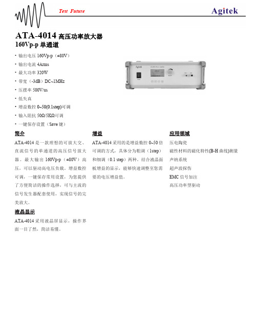
ATA-4014 高压功率放大器
160Vp-p 单通道
• 输出电压 160Vp-p(±80V) • 输出电流 4Arms • 最大功率 320W • 带宽(-3dB)DC~1MHz • 压摆率 500V/us • 低失真 • 增益数控 0~50(0.1step)可调 • 输入阻抗 50Ω/5KΩ可调 • 一键保存设置(Save 键)
Test Future
ATA-4014 高压功率放大器160p-p 单通道规格参数
其他
通道数:
ATA-4014: 单通道输出
输入接口特点:
输入接口:
BNC 接头
输入电阻:
50Ω/5KΩ
输入上限:
10Vp-p
带宽范围:
DC~1MHz (-3dB)
输出接口特点:
输出接口: 输出电阻:
接线柱 不大于 0.125Ω(可定 制)
简介
增益
应用领域
ATA-4014 是一款理想的可放大交、 ATA-4014 采用的是增益数控 0~50 倍 压电陶瓷
直 流信 号的 单通 道的 高压 信号 放大 可调的方式,具体分为粗调(1step) 磁性材料的磁化特性(B-H 曲线)测量
器 。 最 大 输 出 160Vp-p ( ±80V ) 高 和细调(0.1 step)两种。结合液晶面 声纳系统
压,可以驱动高电压负载。增益数控 板增益的显示,能够快速调整至您需 超声波探伤
可调,一键保存常用设置,为您提供 要的电压增益值。
EMC 信号加注
了方便简洁的操作选择,可与主流的
高压功率型驱动
信号发生器配套使用,实现信号的完
美放大。
液晶显示
ATA-4014 采用液晶屏显示,操作界 面一目了然,简洁易懂。
海视晨光DS-2DE4A404IW-DE(2.8-12mm)4MP4×网络红外PTZ摄像头产品介绍说
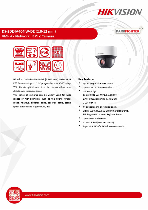
Hikvision DS-2DE4A404IW-DE (2.8-12 mm) Network IR PTZ Camera adopts 1/1.9" progressive scan CMOS chip. With the 4× optical zoom lens, the camera offers more details over expansive areas.This series of cameras can be widely used for wide ranges of high-definition, such as the rivers, forests, roads, railways, airports, ports, squares, parks, scenic spots, stations and large venues, etc.Key Features•1/1.9" progressive scan CMOS•Up to 2560 × 1440 resolution•Ultra-low light:Color: 0.002 Lux @(F1.6, AGC ON)B/W: 0.0002 Lux @(F1.6, AGC ON)0 Lux with IR•4× optical zoom, 16× digital zoom •Digital WDR, HLC, BLC, 3D DNR, Digital Defog, EIS, Regional Exposure, Regional Focus •Up to 50 m IR distance•12 VDC & PoE (802.3at, class4) •Support H.265+/H.265 video compressionCamera ModuleImage Sensor 1/1.9" progressive scan CMOSMin. Illumination Color: 0.002 Lux @(F1.6, AGC ON) B/W: 0.0002Lux @(F1.6, AGC ON) 0 Lux with IRWhite Balance Auto/Manual/ATW (Auto-tracking White Balance)/Indoor/Outdoor/FluorescentLamp/Sodium LampGain Auto/ManualShutter Time 50Hz: 1/1 s to 1/30,000 s60Hz: 1/1 s to 1/30,000 sDay & Night IR Cut FilterDigital Zoom 16×Privacy Mask 24 programmable privacy masksFocus Mode Auto/Semi-automatic/ManualWDR Digital WDRLensFocal Length 2.8 mm to 12 mm, 4× optical zoomZoom Speed Approx. 2.2 s (optical lens, wide-tele)Field of View Horizontal field of view: 69.5° to 26.48° (Wide-Tele) Vertical field of view: 38° to 14.94° (Wide-Tele) Diagonal field of view: 81.2° to 20.38° (Wide-Tele)Working Distance 10 mm to 1500 mm (wide-tele)Aperture Range F1.5 to F2.8IRIR Distance50 mSmart IR YesPTZMovement Range (Pan) 360° endlessPan Speed Configurable, from 0.1°/s to 300°/s. Preset speed: 350°/sMovement Range (Tilt) From -5° to 90° (auto-flip)Tilt Speed Configurable, from 0.1°/s to 160°/s. Preset Speed: 200°/sProportional Zoom YesPresets 300Patrol Scan 8 patrols, up to 32 presets for each patrolPattern Scan 4 pattern scans, record time over 10 minutes for each scanPower-off Memory YesPark Action Preset/Pattern Scan/Patrol Scan/Auto Scan/Tilt Scan/Random Scan/Frame Scan/Panorama Scan3D Positioning YesPTZ Position Display YesPreset Freezing YesScheduled Task Preset/Pattern Scan/Patrol Scan/Auto Scan/Tilt Scan/Random Scan/Frame Scan/Panorama Scan/Dome Reboot/Dome Adjust/Aux OutputCompression StandardVideo Compression Main Stream: H.265+/H.265/H.264+/H.264 Sub-stream: H.265/H.264/MJPEGThird Stream: H.265/H.264/MJPEGH.264 Type Baseline Profile/Main Profile/High Profile H.264+ YesH.265 Type Baseline Profile/Main Profile/High ProfileH.265+ YesVideo Bitrate 256 Kbps to 16384 KbpsAudio Compression G.711alaw/G.711ulaw/G.722.1/G.726/MP2L2/PCMSVC YesSmart FeaturesBasic Event Detection Motion Detection, Alarm Input, Alarm Output, Video Tampering, ExceptionSmart Event Detection Audio Exception Detection, Face Detection, Intrusion Detection, Line Crossing Detection, Region Entrance Detection, Region Exiting Detection, Unattended Baggage Detection, Object Removal DetectionSmart Record ANR (Automatic Network Replenishment), Dual-VCASmart Tracking Manual Tracking, Auto Tracking, Event Tracking, support multi scenes patrol tracking ROI Main stream, sub-stream, and third stream respectively support four fixed areas. ImageMax. Resolution 2560 × 1440Main Stream 50Hz: 25fps (2560 × 1440, 2048 × 1536, 1920 × 1080, 1280 × 960, 1280 × 720) 50fps (1920 × 1080, 1280 × 960, 1280 × 720)60Hz: 30fps (2560 × 1440, 2048 × 1536, 1920 × 1080, 1280 × 960, 1280 × 720) 60fps (1920 × 1080, 1280 × 960, 1280 × 720)Sub-Stream 50Hz: 25fps (704 × 576, 640 × 480, 352 × 288)60Hz: 30fps (704 × 480, 640 × 480, 352 × 240)Third Stream 50Hz: 25fps (1920 × 1080, 1280 × 960, 1280 × 720, 704 × 576, 640 × 480, 352 × 288)60Hz: 30fps (1920 × 1080, 1280 × 960, 1280 × 720, 704 × 480, 640 × 480, 352 × 240) Image Enhancement HLC/BLC/3D DNR/Digital Defog/EIS/Regional Exposure/Regional FocusNetworkNetwork Storage Built-in memory card slot, support Micro SD/SDHC/SDXC, up to 256 GB; NAS (NFS, SMB/ CIFS), ANRAlarm Linkage Alarm actions, such as Notify Surveillance Center, Upload to FTP, Send Email, TriggerRecording, Recording Linkage, and Alarm Input, etc.Protocols IPv4/IPv6, HTTP, HTTPS, 802.1x, Qos, FTP, SMTP, UPnP, SNMP, DNS, DDNS, NTP, RTSP,RTCP, RTP, TCP/IP, UDP, IGMP, ICMP, DHCP, PPPoE, BonjourAPI ONVIF (Profile S, Profile G, Profile T), ISAPI, SDKSimultaneous Live View Up to 20 channelsUser/Host Up to 32 users3 levels: Administrator, Operator and UserSecurity Measures User authentication (ID and PW), Host authentication (MAC address); HTTPS encryption;IEEE 802.1x port-based network access control; IP address filteringClient iVMS-4200, iVMS-4500, iVMS-5200, Hik-ConnectWeb Browser IE 8 to 11, Chrome 31.0+, Firefox 30.0+, Edge 16.16299+InterfaceAlarm Interface 2-ch alarm input and 2-ch alarm outputAudio Interface 1-ch audio input and 1-ch audio outputNetwork Interface 1 RJ45 10 M/100 M Ethernet, PoE (802.3at, class4)GeneralLanguage (Web Browser Access ) 32 languages.English, Russian, Estonian, Bulgarian, Hungarian, Greek, German, Italian, Czech, Slovak, French, Polish, Dutch, Portuguese, Spanish, Romanian, Danish, Swedish, Norwegian, Finnish, Croatian, Slovenian, Serbian, Turkish, Korean, Traditional Chinese, Thai, Vietnamese, Japanese, Latvian, Lithuanian, Portuguese (Brazil)Power 12 VDC, 3.33 A and PoE (802.3at), 42.5 to 57 VDC, 0.6 A, class4Max.: 18 W, including max. 5.5W for IRWorking Temperature Outdoor: -30°C to 65°C (-22°F to 149°F)Working Humidity ≤ 90%Protection Level IP66 Standard; 4000V Lightning Protection, Surge Protection and Voltage Transient ProtectionInstallation Variable installation methods optional, including ceiling mounting (default), in-ceiling mounting, pendant mounting and wall mounting Material Aluminum AlloyDimensions Φ 169 mm × 161 mm (Φ 6.65" × 6.34") WeightApprox. 2.45 kg (5.40 lb)DORIThe DORI (detect, observe, recognize, identify) distance gives the general idea of the camera ability to distinguish persons or objects within its field of view.DORI Detect Observe Recognize Identify Definition 25 px/m 63 px/m 125 px/m 250 px/m Distance (Tele)216.7 m (710.8 ft)86.0 m (282.1 ft)43.3 m (142.2 ft)21.7 m (71.1 ft)Available ModelDS-2DE4A404IW-DE (2.8-12 mm)DimensionsUnit: mm161Φ169Accessory Included:KPL-040F-VIPower adapter Optional:DS-1605ZJ Wall Mount BracketDS-1275ZJ-SUSVertical pole mountDS-1276ZJ-SUSCorner mountDS-1691ZJ-LPendant MountDS-1691ZJ-M Pendant MountDS-1691ZJPendant MountDS-1671ZJ-SD11In-ceiling Mount BracketDS-1280ZJ-SD11Junction BoxLAS60-57CN-RJ45 Hi-PoE midspanDS-1100KINetwork KeyboardDS-1005KIUSB Joy-stick05060020201109。
FLUKE Ti40 50 45 55 说明书

®Ti40, Ti45, Ti50, Ti55IR FlexCam Thermal Imager用户手册May 2006, Rev.1, 8/06 (Simplified Chinese)2006 Fluke Corporation, All rights reserved.All product names are trademarks of their respective companies.有限担保和有限责任Fluke 担保在正常使用和保养的情况下,其产品没有材料和工艺上的缺陷。
两年的担保期间由产品发货之日算起。
部件、产品修理和服务的担保期限为 90 天。
本担保仅限于Fluke 授权零售商的原购买人或最终用户,并且不适用于一次性电池、电缆接头、电缆绝缘转换接头或 Fluke 认为由于误用、改装、疏忽、污染及意外或异常操作或处理引起的任何产品损坏。
Fluke 担保软件能依照功能规格正常运行 90 天,并且软件是记录在无缺陷的媒介上。
Fluke 并不担保软件毫无错误或在运行中不会中断。
Fluke 授权的零售商应仅对最终用户就新的和未使用的产品提供本担保,但无权代表Fluke 公司提供额外或不同的担保。
只有通过 Fluke 授权的销售店购买的产品或者买方已经按适用的国际价格付款才能享受 Fluke 的担保支持。
在一国购买的产品需在他国修理时,Fluke 有权向买方要求负担重大修理/零件更换费用。
Fluke 的担保为有限责任,由 Fluke 决定是否退还购买金额、免费修理或更换在担保期间退还 Fluke 授权服务中心的故障产品。
如需要保修服务,请与您就近的 Fluke 授权服务中心联系,获得退还授权信息;然后将产品寄至服务中心,并附上产品问题描述,同时预付运费和保险费(目的地离岸价格)。
Fluke 不承担运送途中发生的损坏。
在保修之后,产品将被寄回给买方并提前支付运输费(目的地交货)。
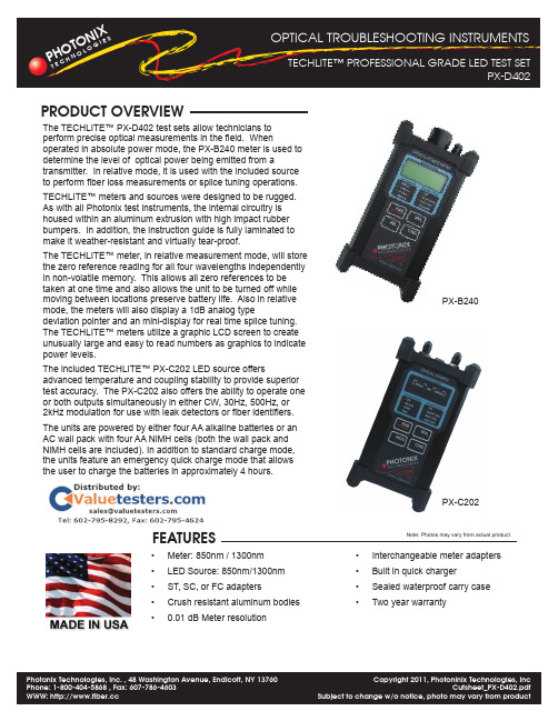
Photonix PX-D402 LED光电测试设备说明书
Photonix Technologies, Inc. , 48 Washington Avenue, Endicott, NY 13760 Phone: 1-800-404-5868 , Fax: 607-786-4603 WWW:
Copyright 2011, Photoninix Technologies, Inc Cutsheet_PX-D402.pdf
TECHLITE™ PROFESSIONAL GRADE LED TEST SET PX-D402
POWER METER PX-B240 Parameter Detector Wavelength Power Range(1300-1550nm) Power Rance(850nm) Resolution Accuracy Display Backlight Auto Power Off Storage Points
Value Germanium 850,1300,1310,1550nm +3 to -60dBm +8 to -55dBm 0.01dB +/-0.25dB dB,dBm Variable Variable 999 per wavelength
LED SOURCE PX-C202 Parameter Emitter Wavelength Pout Stability(8hr) Bandwidth (typ) Modulation
The units are powered by either four AA alkaline batteries or an AC wall pack with four AA NiMH cells (both the wall pack and NiMH cells are included). In addition to standard charge mode, the units feature an emergency quick charge mode that allows the user to charge the batteries in approximately 4 hours.
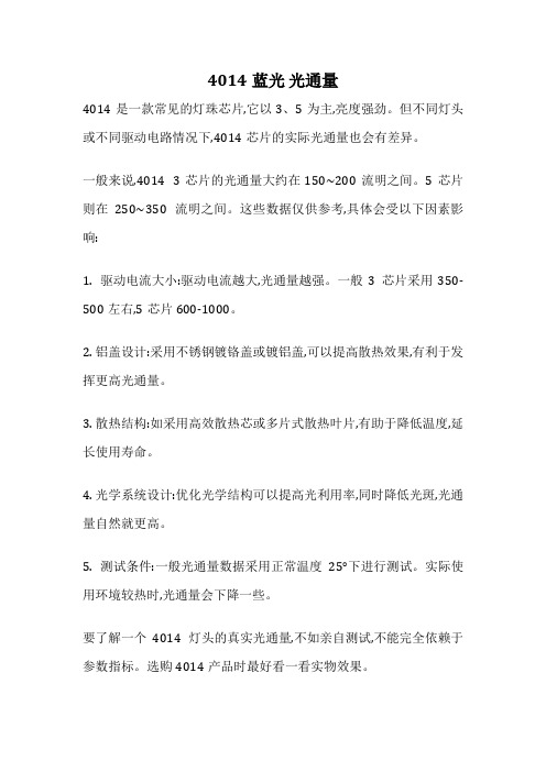
灯珠4014

80 70 60
Forward Current(mA)
Relative Luminous Intensity
1.5 2.0
Forward Current VS. Relative Intensity
正向电流与相对光强特性曲线
50 40 30 20 10 0 0 20 40 60 80 100
Package Dimensions(封装尺寸)
1
2
Recommended Soldering Pattern (建议焊盘尺寸图)
1
2
1
Notes:(备注) 1. All dimension units are millimeters.( 所有标注尺寸单位为毫米) 2.All dimension tolerance is ±0.15mm unless otherwise noted. ( 除特别标注外,所有尺寸允许公差 ±0.15mm )
RoHS
Specification
规 格 书
Customer Name:
客户名称:
Customer P/N:
客户品号:
Factory P/N: A-4014HW-S1-PCT
公司品号:
Sending Date:
送样日期:
Client approval
客户审核
Hongli approval
鸿利光电审核
Applications(应用)
■ Optical indicator (光学指示) ■ Indoor display(室内显示) ■ Automotive lighting(汽车照明) ■ Backlight for LCD, switch and Symbol, display (LCD背光、转换器,开关和标志,显示器等) ■ Tubular light application (用于日光灯管) ■ General use(一般应用)
有线电视网络智能机顶盒(IP型)测量方法GD∕J 114-2020

目次前言 (II)1 范围 (1)2 规范性引用文件 (1)3 术语、定义和缩略语 (1)3.1 术语和定义 (1)3.2 缩略语 (1)4 测量方法 (2)4.1 主芯片、GPU、RAM、Flash (2)4.2 视、音频解码 (2)4.3 输出显示 (2)4.4 WiFi能力 (3)4.5 蓝牙模块、红外接收 (3)4.6 硬件接口、以太网络接口、电源、操作系统、设备号、协议、运行环境及功能组件、媒体播放及封装、应用程序及安全 (4)4.7 视音频技术指标 (4)4.8 HDMI输出 (4)4.9 复合视频输出 (4)4.10 4K输出音频 (6)4.11 日志功能 (9)4.12 升级功能 (10)4.13 整机待机功率 (10)4.14 交流电供电 (10)4.15 直流电供电 (11)参考文献 (12)有线电视网络智能机顶盒(IP型)测量方法1 范围本技术文件规定了符合GD/J 078—2018的有线电视网络智能机顶盒(IP型)(以下简称“智能机顶盒”)的测量方法。
本技术文件适用于具备基本视频播放功能,能够运行智能化应用的智能机顶盒,以及其他具有广电宽带电视接收功能设备的检测。
2 规范性引用文件下列文件对于本文件的应用是必不可少的。
凡是注日期的引用文件,仅注日期的版本适用于本文件。
凡是不注日期的引用文件,其最新版本(包括所有的修改单)适用于本文件。
GD/J 078—2018 有线电视网络智能机顶盒(IP型)技术要求3 术语、定义和缩略语3.1 术语和定义下列术语和定义适用于本文件。
3.1.1有线电视网络智能机顶盒(IP型) internet-protocol-based cable TV smart set top box 搭载智能操作系统,支持应用程序安装和卸载,支持数字电视广播、互联网接入、互联网业务、应用商店、电子支付等功能的机顶盒。
3.2 缩略语下列缩略语适用于本文件。
AP 接入点(Access Point)CVBS 复合视频广播信号(Composite Video Broadcast Signal)GPU 图形处理器(Graphics Processing Unit)HDMI 高清晰度多媒体接口(High Definition Multimedia Interface)HDTV 高清晰度电视(High Definition Television)IP 互联网协议(Internet Protocol)RAM 随机存取存储器(Random Access Memory)SDTV 标准清晰度电视(Standard Definition Television)USB 通用串行总线(Universal Serial Bus)UHDTV 超高清晰度电视(Ultra High Definition Television)WiFi 无线网络(Wireless Fidelity)GD/J 114—20204 测量方法4.1 主芯片、GPU、RAM、Flash4.1.1 测量框图测量框图见图1。
ADI公司推出业内甚低噪声精密四放大器显著减少了功耗和封装尺寸

ADI公司推出业内甚低噪声精密四放大器显著减少了功耗和
封装尺寸
佚名
【期刊名称】《电子测量技术》
【年(卷),期】2005()3
【摘要】美国模拟器件公司低噪声的双极型精密四放大器ADA4004—4,以适应多通道数据采集、分析仪表、自动测试设备以及其它±18V电源电压工作的工业和医用系统的严格要求。
采用ADI公司新的iPOLARTM[链接到新闻稿]沟道隔离制造工艺生产的ADA4004—4放大器能使器件的功耗比同类器件减小50%,其芯片级封装尺寸减小到70%。
ADA4004—4兼备低功耗和小尺寸的特性使其能保持优良的动态范围.而无需同类器件必需的散热风扇或散热片,
【总页数】1页(P98-98)
【关键词】ADI公司;封装尺寸;放大器;低噪声;精密;美国模拟器件公司;多通道数据采集;推出;自动测试设备;分析仪表;电源电压;工艺生产;散热风扇;动态范围;双极型;芯片级;散热片;小尺寸;低功耗;减小;同类
【正文语种】中文
【中图分类】TN792;TM564
【相关文献】
1.ADI公司36V低噪声精密放大器 [J],
2.Intersil推出低噪声低功耗40V四通道精密放大器 [J], 江兴;
3.ADI公司的放大器为便携式应用提供高精度、小尺寸和低功耗特性 [J],
4.ADI公司推出适于工业和仪表设备使用的业内甚低噪声36V放大器 [J],
5.ADI公司推出大型RF放大器Sys-Parameter模型库-ADI公司用于Keysight Technologies Genesys软件的Sys-Parameter库显著简化RF设计 [J],
因版权原因,仅展示原文概要,查看原文内容请购买。
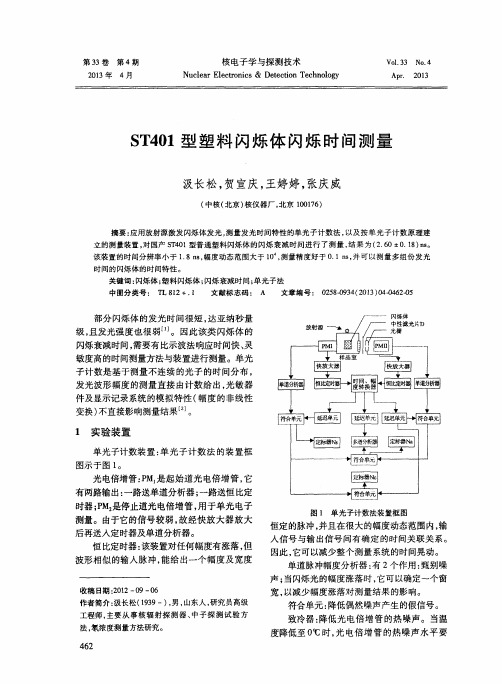
ST401型塑料闪烁体闪烁时间测量
2 工 作 原 理
光 电转换 : 为 了分 析闪烁 体发射 的闪烁光
强度按时间的分布 , 需要把闪烁光变为电信号 , 然后 用 电子 学 仪 器 记 录 和 显 示 J 。 光 电转 换
是 由光 电倍 增 管实 现 的 。发光 物 质发 出的光 子 落 在光 电倍 增 管 光 阴极 上 产 生 光 电 子 ; 光 电子
S T 4 0 1型 塑 料 闪 烁 体 闪 烁 时 间 测 量
汲长松 , 贺宣庆 , 王婷婷 , 张庆威
( 中核 ( 北京 ) 核 仪器厂 , 北京 1 0 0 1 7 6 )
摘 要: 应用放射 源激发 闪烁 体发光 , 测量发 光时问特 性的单光 子计数法 , 以及 按单光子计 数原 理建
后再 送入 定时器 及单道 分 析器 。
图 1 单 光子计数法装置框 图
恒定 的脉冲, 并且在很大的幅度动态范围内, 输 入信号与输 出信号间有确定 的时间关联关系。 因此, 它可以减少整个测量系统的时间晃动。 单道脉 冲幅度分析器 : 有2 个作用 : 甄别噪
声; 当闪烁 光 的幅度 涨落 时 , 它可 以确定 一个 窗
数据 。 样 品室 : 放置样品。
度选道存储 。这样 , 经过多次激发测量后 , 多道 分析器 中就得到一个谱 N ( t ) 。其道数对应 的 是时间间隔。每道 中的计数对应于多次激发中 P M : 在相应的时间探测到单个光子的次数。单 道分析器和符合单元用于甄别噪声本底和选择 满足 一定 条 件 的 激 发 事件 ; 恒 比定 时 器用 于减
通过光 电倍增管 内的光学收集 系统 , 将其聚焦 到第一倍增级上并产生二 次电子 ; 随后经多级 倍增; 最后 , 电子束被 阳极收集形成 阳极电流或 电压 。 光电倍增 管 P M 与待测 发光样 品光学耦 合, 每次闪烁都给出一个信号 ; 该信号经恒 比定 时器作为起始参考信号送人时间一 幅度变换器
4014蓝光 光通量
4014蓝光光通量
4014是一款常见的灯珠芯片,它以3、5为主,亮度强劲。
但不同灯头或不同驱动电路情况下,4014芯片的实际光通量也会有差异。
一般来说,4014 3芯片的光通量大约在150~200流明之间。
5芯片则在250~350流明之间。
这些数据仅供参考,具体会受以下因素影响:
1. 驱动电流大小:驱动电流越大,光通量越强。
一般3芯片采用350-500左右,5芯片600-1000。
2. 铝盖设计:采用不锈钢镀铬盖或镀铝盖,可以提高散热效果,有利于发挥更高光通量。
3. 散热结构:如采用高效散热芯或多片式散热叶片,有助于降低温度,延长使用寿命。
4. 光学系统设计:优化光学结构可以提高光利用率,同时降低光斑,光通量自然就更高。
5. 测试条件:一般光通量数据采用正常温度25°下进行测试。
实际使用环境较热时,光通量会下降一些。
要了解一个4014灯头的真实光通量,不如亲自测试,不能完全依赖于参数指标。
选购4014产品时最好看一看实物效果。
LED面板灯结构及工作原理ppt课件

以上,请品质来料检验时及生产过程中注意若有与以上抛光方式不符,则判为不良。
拟制: 会签意见栏:
□国际营销中心
□国内营销中心
□人事行政部
□财务部 相 □计划 关 单 □仓库 位 □工程部 会 □品质部 签 栏 □生产部
□研发部
□采购
□运营中心
□总经办
审核:
日期:
ST001-D
ppt精选版
12
导光板加工需要注意什么呢? 1.擦拭的白电油过多,长时间不干形成白印不良(在无明显白点黑点的情况
PMMA原料模压而成,无需经过后道处理,产品的一致性和良率都为 100%,由于光线在导光板内部发生全反射,出光率也高于传统网点导光 板。而我司新的供应商天宇力程,导光板为单面微结构加丝印网点,网点
面为反射面,微结构面为出光面.
免丝印
丝印网点
ppt精选版
9
光线在导光板里面前进的方式是类似乒乓球一样在上下面间波浪前进的,
面板灯结构及工作原理
ppt精选版
编制: 蔡治勇 2016.09.01
1
❖ LED面板灯是一款以LED为光源的高档室内照明灯具。整个 灯具设计美观简洁、大气豪华,既有良好的照明效果,又能 给人带来美的感受。LED面板灯设计独特,电源将市电转化 为适合灯珠工作的直流电,驱动灯珠发光,光经过高透光率 的导光板后形成一种均匀的平面发光效果,再经过扩散板扩 散后形成照度均匀性好,光线柔和、舒适而不失明亮,可有 效缓解眼疲劳。LED面板灯还能防辐射,不会刺激孕妇、老 人、儿童的皮肤。
15
五.EVA
❖ EVA和海绵起固定的作用。 其中EVA的价格贵,阻燃;海绵,珍珠棉不阻燃,所以出口时该国家对安
规要求的就只能用EVA. EVA的尺寸规格必须与工单要求一致。 1.EVA尺寸过大,垫在框体上,会压不紧导光板扩散板,使导光板和扩散板
401型光弹仪与APPLE—II+微机的联接

401型光弹仪与APPLE—II+微机的联接
严开丰;徐有刚
【期刊名称】《核工业自动化》
【年(卷),期】1992(000)002
【总页数】3页(P23-25)
【作者】严开丰;徐有刚
【作者单位】不详;不详
【正文语种】中文
【中图分类】O348.1
【相关文献】
1.WKC—1型孔内光弹应力条纹记录仪 [J], 候峰云
2.401型光弹仪与APPLE—Ⅱ+微机的连结 [J], 严开丰
3.微机辅助自动光弹仪实现"盲区"测试自动化 [J], 彭晓东;秦晓桐
4.RCG401型消化弹、烟幕弹改进技术通过部级鉴定 [J], 王绘臣
5.ECL-1型电致化学发光仪与APPLE-Ⅱ微机的联用 [J], 林金明;安镜如;郑新;胡垚因版权原因,仅展示原文概要,查看原文内容请购买。
4合一光罩 半导体

光罩(也称为光掩模)是用于制造集成电路的重要工具,它决定了集成电路的图案和形状。
光罩由石英玻璃制成,具有极高的透明度,并且在制造过程中需要进行精细的加工和清洗。
在制造集成电路的过程中,光罩被放置在硅片上,通过曝光和显影等过程,将光罩上的图案转移到硅片上。
而4合1光罩是一种将4个芯片或器件的图案集成到一个光罩上的技术。
这种技术的应用可以减少光罩的数量,从而降低制造成本和生产时间。
同时,由于减少了光罩的数量,也减少了制造过程中的误差和缺陷的可能性。
在半导体领域中,4合1光罩技术的应用越来越广泛。
例如,在制造液晶显示器、LED灯、太阳能电池等产品时,常常需要用到这种技术。
通过将多个芯片或器件的图案集成到一个光罩上,可以大大提高生产效率和降低成本。
总的来说,4合1光罩技术是一种重要的半导体制造技术,它可以提高生产效率、降低成本,并且有助于推动半导体产业的发展。
405nm四分之一波片

405nm四分之一波片
405nm四分之一波片是一种光学元件,通常由蓝光滤光片制成。
它可以选择性地传递或阻挡405nm波长的光线,而将其他波
长的光线完全或部分反射掉。
四分之一波片的设计原理基于光的偏振状态,它可以将入射光线分解为垂直方向和平行方向的两个分量,实现对光的控制与调节。
四分之一波片被广泛应用于激光器、光学仪器、显微镜和光学通信等领域。
在激光器中,它可以将线性偏振光转换为圆偏振光或逆时针偏振光,用于特定的实验或应用。
在显微镜中,四分之一波片可以用于分辨光学图像中的细节,提高成像的质量。
在光学通信中,它可以用于光信号的调制和解调,提高信号的传输效率和稳定性。
总之,405nm四分之一波片是一种重要的光学元件,它可以实现对光的偏振状态的调节和控制,广泛应用于光学领域中的各种应用中。
- 1、下载文档前请自行甄别文档内容的完整性,平台不提供额外的编辑、内容补充、找答案等附加服务。
- 2、"仅部分预览"的文档,不可在线预览部分如存在完整性等问题,可反馈申请退款(可完整预览的文档不适用该条件!)。
- 3、如文档侵犯您的权益,请联系客服反馈,我们会尽快为您处理(人工客服工作时间:9:00-18:30)。
超薄面板灯光学报告1.超薄面板灯外观图
2.超薄面板灯结构尺寸图
3.超薄面板灯裸光源总光通量计算
以我司供应商4014灯珠为例,如下图(4014灯珠规格书截图):
由此可见,4014单颗灯珠色温3000K和4000K的光通量供应商建议取值为20LM和21LM。
那么,一颗灯珠,暖白色温3000K为20LM每颗灯,若36W面板灯使用192PCS灯珠,那么暖白色温,36W面板灯的光通量即为20lm*192=3840LM;自然白4000K为21LM每颗灯,若36W面板灯使用192PCS灯珠,那么暖自然白色温,36W面板灯的光通量即为21lm*192=4032LM.
4.依照灯具结构影响光效还有如下因素:
A.导光板理想透光率为90%,此处会损失10%的光通量;
B.扩散板,PS材质理想透光率85%,此处会损失15%的光通量;
C.反射膜光反射率96%,此处会损失4%的光通量;
由此理论上总光通量Φ=4032x0.9x0.85x0.96=2961.1LM
我司光色电综合测试仪测试所得总光通量如下:
由此可见理论值与实测值还有一些偏差,这是因为LED灯珠点亮后,温度会升高,光通量便有所下降,如果用积分球测试,会相对较高,这是因为积分球测试温度很短,只有几分钟,灯具温度还没有稳定下来,散热器表面温度还没有达到稳定状态。
灯珠光通量与温度的关系可以从下图说明(灯珠厂商4014灯珠规格书截图):
因为温度所损耗的光通量Φ=1-2820/2961=4.8%,这个数值合乎目前LED灯珠散热水平。