2N915中文资料
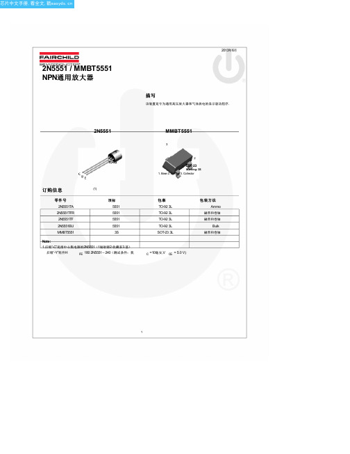
2N5551中文资料(fairchild)中文数据手册「EasyDatasheet - 矽搜」
50 VCB = 100V
10
10
10
1β
100 Co
o
125 C
0.1
o
-40 Co
25 Co
75 C
- CCEO(SALT)LECTOR-EMITTER VOLTAGE [V]
0.01
V
1
10
100
IC- COLLECTOR CURRENT [mA]
Figure 2. Collector-Emitter Saturation Voltage vs.
芯片中文手册,看全文,戳
2N5551 / MMBT5551 NPN通用放大器
2013年6月
描写
该装置是专为通用高压放大器和气体放电的显示驱动程序.
2N5551
TO-92
MMBT5551
3
2
1 SOT-23
Marking: 3S 1. Base 2. Emitter 3. Collector
MMBT5551
350 2.8
357
Units
mW mW/°C °C/W °C/W
2
芯片中文手册,看全文,戳
电气特性
(4)
价值观是在T 符
A = 25°C除非另有说明. 参数
断特性
V(BR)CEO 集电极 - 发射极击穿电压 V(BR)CBO 集电极基击穿电压 V (BR)EBO 发射极基极击穿电压
Value
160 180
6 600 -55到+150
2N5551 / MMBT5551 - NPN通用放大
器
Units
V V V mA °C
热特性
价值观是在T
2N1595中文资料
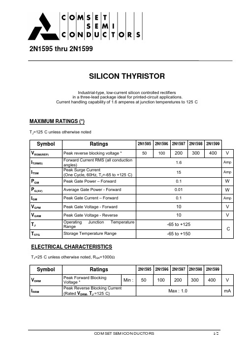
2N1595 thru 2N1599SILICON THYRISTORIndustrial-type, low-current silicon controlled rectifiersin a three-lead package ideal for printed-circuit applications.Current handling capability of 1.6 amperes at junction temperetures to 125°CMAXIMUM RATINGS (*)T J=125°C unless otherwise notedSymbol Ratings2N15952N15962N15972N15982N1599V RSM(REP)Peak reverse blocking voltage *50100200300400VI T(RMS)Forward Current RMS (all conduction1.6Ampangles)I TSM Peak Surge Current15Amp (One Cycle, 60Hz, T J=-65 to +125°C)P GM Peak Gate Power – Forward0.1W P G(AV)Average Gate Power - Forward0.01W I GM Peak Gate Current – Forward0.1Amp V GFM Peak Gate Voltage - Forward10V V GRM Peak Gate Voltage - Reverse10V T J Operating Junction Temperature-65 to +125Range°C T STG Storage Temperature Range-65 to +150ELECTRICAL CHARACTERISTICST J=25°C unless otherwise noted, R GK=1000ΩSymbol Ratings2N15952N15962N15972N15982N1599V DRM Peak Forward BlockingMin :50100200300400V Voltage *I RRM Peak Reverse Blocking CurrentMax : 1.0mA (Rated V DRM, T J =125°C)2N1595 thru 2N1599Symbol Ratings2N15952N15962N15972N15982N1599I DRM Peak Forward Blocking Current(Rated V DRM with gate open , T J=125°C)Max :1.0mAI GT Gate Trigger Current (2)Anode Voltage=7.0 Vdc, R L=12ΩTyp : 2.0Max : 10mAGate Trigger VoltageAnode Voltage=7.0 Vdc, R L=12ΩTyp : 0.7Max : 3.0V GTV DRM= Rated, R L=100Ω, T J=125°C Min : 0.2VI H Holding CurrentAnode Voltage=7.0 Vdc, gate open Typ : 5.0mAV TM Forward On VoltageI T=1 AdcTyp : 1.1Max : 2.0Vt gt Turn-On Time (t d+t r)I GT=10 mA, I T=1 A Typ : 0.8µst q Turn-Off TimeI T=1 A, I R =1 A, dv/dt=20 V/µs,T J=125°CV DRM= Rated VoltageTyp : 10µs* V DRM or V RSM can be applied for all types on a continuous dc basis without incurring damage. MECHANICAL DATA CASE TO-39DIMENSIONSmm inchesA6,250,24B13,590,53C9,240,36D8,240,32E0,780,03F1,050,041G0,420,165H45°L5,10,2Pin 1 :CathodePin 2 :GatePin 3 :AnodeInformation furnished is believed to be accurate and reliable. However, CS assumes no responsability for the consequences of use of such information nor for errors that could appear.Data are subject to change without notice.。
场效应管参数
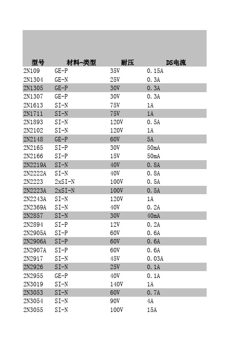
SI-N SI-N SI-P SI-N SI-P P-DARL+D SI-N SI-N SI-N SI-N SI-P SI-P SI-P SI-P SI-P N-DARL P-DARL SI-N N-DARL SI-P N-DARL SI-P SI-N SI-P SI-N SI-P SI-N SI-P SI-P N-FET N-FET SI-N SI-N
SI-N SI-P P-FET N-FET SI-P N-FET SI-N SI-P SI-P GE-P SI-P N-FET SI-P GE-P GE-P SI-N SI-N SI-P N-FET SI-N SI-N N-FET N-FET N-FET N-FET SI-N SI-P N-FET SI-N SI-N SI-P SI-P SI-N
2SA1120 SI-P 2SA1123 SI-P 2SA1124 SI-P 2SA1127 SI-P 2SA1141 SI-P 2SA1142 SI-P 2SA1145 SI-P 2SA1150 SI-P 2SA1156 SI-P 2SA1160 SI-P 2SA1163 SI-P 2SA1170 SI-P 2SA1185 SI-P 2SA1186 SI-P 2SA1200 SI-P 2SA1201 SI-P 2SA1206 SI-P 2SA1207 SI-P 2SA1208 SI-P 2SA1209 SI-P 2SA1210 SI-P 2SA1213 SI-P 2SA1215 SI-P 2SA1216 SI-P 2SA1220A SI-P 2SA1221 SI-P 2SA1225 SI-P 2SA1227A SI-P 2SA1232 SI-P 2SA1241 SI-P 2SA1242 SI-P 2SA1244 SI-P 2SA1249 SI-P
2N5401中文资料
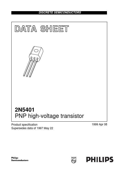
SYMBOL
PARAMETER
CONDITIONS
MIN.
ICBO
IEBO hFE
VCEsat
Cc fT F
collector cut-off current
IE = 0; VCB = −120 V
−
IE = 0; VCB = −120 V; Tamb = 100 °C
−
emitter cut-off current
OUTLINE
VERSION
IEC
REFERENCES
JEDEC
EIAJ
EUROPEAN PROJECTION
SOT54
TO-92
SC-43
ISSUE DATE 97-02-28
1999 Apr 08
5
元器件交易网
Philips Semiconductors
PNP high-voltage transistor
IC = 0; VEB = −4 V
−
DC current gain
IC = −1 mA; VCE = −5 V; see Fig.2
50
IC = −10 mA; VCE = −5 V; see Fig.2
60
IC = −50 mA; VCE = −5 V; see Fig.2
50
collector-emitter saturation voltage IC = −10 mA; IB = −1 mA
IC mA
−103
1999 Apr 08
4
元器件交易网
Philips Semiconductors
PNP high-voltage transistor
2N5401中文资料(motorola)中文数据手册「EasyDatasheet - 矽搜」
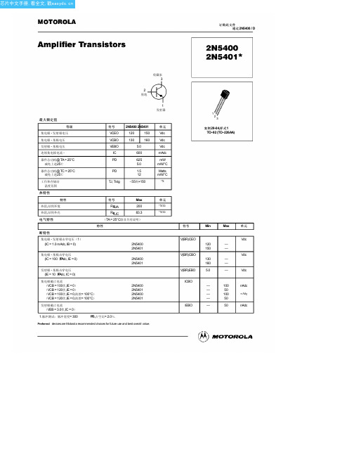
INCHES
DIM MIN MAX A 0.175 0.205 B 0.170 0.210 C 0.125 0.165 D 0.016 0.022 F 0.016 0.019 G 0.045 0.055 H 0.095 0.105 J 0.015 0.020 K 0.500 ––– L 0.250 ––– N 0.080 0.105 P ––– 0.100 R 0.115 ––– V 0.135 –––
小信号特性
电流 - 增益 - 带宽产品 (IC = 10 MADC,VCE = 10伏直流,F = 100兆赫)
输出电容
(VCB = 10 VDC,IE = 0,F = 1.0兆赫)
小信号电流增益
(IC = 1.0 MADC,VCE = 10伏直流,F = 1.0千赫)
噪声系数
(IC = 250 µAdc, VCE = 5.0伏,RS = 1.0千欧,F = 1.0千赫)
IC
600
PD
625
5.0
器件总功耗@ TC = 25°C 减免上述25℃
PD
1.5
12
工作和存储结 温度范围
TJ, Tstg - 55到+150
热特性
特性
符号
Max
热阻,结到环境 热阻,结到外壳
电气特性
RqJA
200
RqJC
83.3
(TA = 25°C除非另有说明)
特性
断特性
集电极 - 发射极击穿电压(1) (IC = 1.0 mAdc, IB = 0)
0.1
0 0.1 0.2 0.3 0.5 1.0 2.0 3.0 5.0
10 20 30 50 100
IC,集电极电流(mA)
2N5109中文资料(Central Semiconductor)中文数据手册「EasyDatasheet - 矽搜」
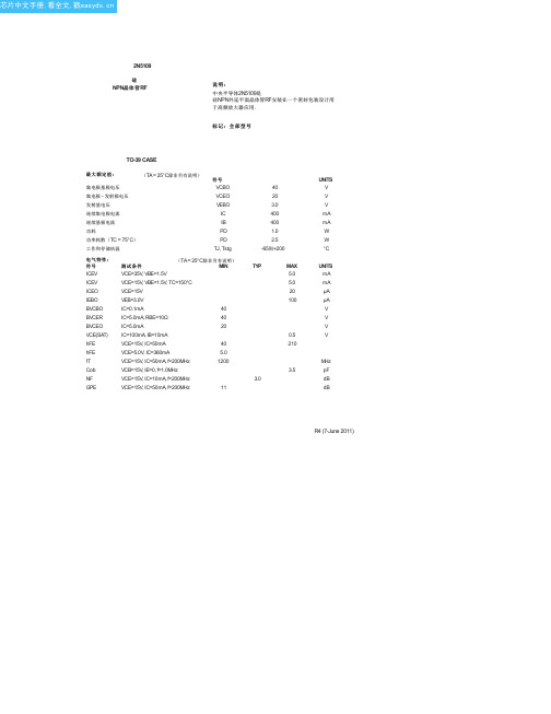
工作和存储结温
符号
VCBO VCEO VEBO
IC IB PD PD TJ, Tstg
电气特性: 符号
ICEV ICEV ICEO IEBO BVCBO BVCER BVCEO VCE(SAT) hFE hFE fT Cob NF GPE
测试条件
VCE=35V, VBE=1.5V
5.0
VCE=15V, IC=50mA, f=200MHz
1200
VCB=15V, IE=0, f=1.0MHz
VCE=15V, IC=10mA, f=200MHz
VCE=15V, IC=50mA, f=200MHz
11
40 20 3.0 400 400 1.0 2.5 -65到+200
TYP
MAX
5.0
5.0
20
100
0.5 210
3.5 3.0
UNITS V V V mA mA W W °C
UNITS mA mA μA μA V V V V
MHz pF dB dB
R4 (7-June 2109
硅
NPN晶体管 RF
TO-39 CASE - 机械外形
前导码:
1)发射 2)基 3)集电极
标记:全部型号
R4 (7-June 2011)
(TA = 25°C除非另有说明) MIN
VCE=15V, VBE=1.5V, TC=150°C
VCE=15V
VEB=3.0V
IC=0.1mA
40
IC=5.0mA, RBE=10Ω
40
IC=5.0mA
20
IC=100mA, IB=10mA
2N5551中文资料_数据手册_参数

Packing Method Ammo
Tape and Reel Tape and Reel
Bulk Tape and Reel
© 2009 Fairchild Semiconductor Corporation
Top Mark 5551 5551 5551 5551 3S
Package TO-92 3L TO-92 3L TO-92 3L TO-92 3L SOT-23 3L
Note: 1. Suffix “-C” means Center Collector in 2N5551 (1. Emitter 2. Collector 3. Base)
Symbol
Parameter
Value
Units
VCEO VCBO VEBO
IC TJ, Tstg(2)
Collector-Emitter Voltage Collector-Base Voltage Emitter-Base Voltage Collector current - Continuous Junction and Storage Temperature
2N5551 / MMBT5551 Rev. 1.1.0
1
2N5551 / MMBT5551 — NPN General-Purpose Amplifier
Absolute Maximum Ratings(2)
Stresses exceeding the absolute maximum ratings may damage the device. The device may not function or be operable above the recommended operating conditions and stressing the parts to these levels is not recommended. In addition, extended exposure to stresses above the recommended operating conditions may affect device reliability. The absolute maximum ratings are stress ratings only. Values are at TA = 25°C unless otherwise noted.
2SA1015中文资料(Unisonic Technologies)中文数据手册「EasyDatasheet - 矽搜」
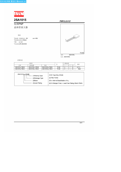
BL 350-700
2of 4
芯片中文手册,看全文,戳
2SA1015
典型特征
静态特性
-50
-40
I =-300µA
-30 I =-250µA
-20
I =-200µA
I =-150µA
-10
I =-100µA
I =-50µA
0
-0
-4 -8 -12 -16 -20
集电极 - 发射极电压,BV
饱和电压
-10 I =10xI
-10 -10 (mA)
-10
V
-10
V
-10 -10
-10 -10 集电极电流,I
集电极输出电容
-10 f=1MHz -10 I =0
-10 -10 (mA)
-10
-10
-10
-10
-10
-10
集电极基极电压,BV
-10 (V)
3of 4
芯片中文手册,看全文,戳
4of 4
FE1
Y 120-240
GR 200-400
额定值
单元
-50
V
-50
V
-5
V
-150
mA
-50
mA
400
mW
125
°C
-55 ~ +125
°C
MIN TYP 最大单位
-50
V
-50
V
-5
V
-100 nA
-100 nA
120
700
25
-0.1 -0.3 V
-1.1 V
4.0 7.0 pF
80
MHz
0.5 6 dB
2N6668;中文规格书,Datasheet资料

2N6668SILICON PNP POWER DARLINGTON TRANSISTORsSTMicroelectronics PREFERRED SALESTYPEs PNP DARLINGTONsINTEGRATED ANTIPARALLEL COLLECTOR-EMITTER DIODEAPPLICATIONS: s GENERAL PURPOSE SWITCHINGs GENERAL PURPOSE SWITCHING AND AMPLIFIERDecember 2000ABSOLUTE MAXIMUM RATINGS®1/4s Pr od u c t () -l s lOb so e t ePr od u c t () -O bs o e t eP THERMAL DATAELECTRICAL CHARACTERISTICS (T case = 25 oC unless otherwise specified)For PNP type voltage and current values are negative.2N66682N6668l s l c )Ob so e t ePr od u c t () -O bs o e t eP r od u t (sInformation furnished is believed to be accurate and reliable. However, STMicroelectronics assumes no responsibility for the consequences of use of such information nor for any infringement of patents or other rights of third parties which may result from its use. No license is granted by implication or otherwise under any patent or patent rights of STMicroelectronics. Specification mentioned in this publication are subject to change without notice. This publication supersedes and replaces all information previously supplied. STMicroelectronics products are not authorized for use as critical components in life support devices or systems without express written approval of STMicroelectronics.The ST logo is a trademark of STMicroelectronics© 2000 STMicroelectronics – Printed in Italy – All Rights ReservedSTMicroelectronics GROUP OF COMPANIESAustralia - Brazil - China - Finland - France - Germany - Hong Kong - India - Italy - Japan - Malaysia - Malta - Morocco - Singapore - Spain - Sweden - Switzerland - United Kingdom - U.S.A.2N6668分销商库存信息: STM2N6668。
915nm半导体激光器

915nm半导体激光器915nm半导体激光器是一种常见的激光器,它具有高效率、高功率、高可靠性等优点,被广泛应用于医疗、工业、通信等领域。
本文将从915nm半导体激光器的基本原理、结构、性能、应用等方面进行介绍。
一、基本原理915nm半导体激光器是利用半导体材料的特性产生激光。
当外加电压时,半导体材料中的电子和空穴在p-n结区域内结合,产生光子,即激光。
这种激光具有单色性、相干性、直线偏振性等特点。
915nm激光的波长在红外区域,是近红外激光的一种,其主要特点是能够穿透深度较浅的组织,被广泛应用于医疗美容领域。
二、结构915nm半导体激光器的结构主要包括激光芯片、光纤耦合器、控制电路等部分。
其中,激光芯片是整个激光器的核心部分,由p 型和n型半导体材料构成,中间夹杂着一层多量子阱结构。
光纤耦合器用于将激光输出到光纤中,控制电路则用于控制激光器的工作状态。
三、性能915nm半导体激光器具有许多优异的性能,其中最为突出的是高效率、高功率、高可靠性等。
其光电转换效率可以达到50%以上,功率可达到数十瓦,且寿命长、稳定性好。
此外,915nm激光的波长与水分子吸收峰相近,可以被水分子吸收,因此被广泛应用于医疗领域,如激光降压、激光治疗等。
四、应用915nm半导体激光器的应用范围非常广泛,主要包括医疗、工业、通信等领域。
在医疗领域,915nm激光被广泛应用于激光降压、激光治疗、激光美容等方面。
在工业领域,915nm激光被广泛应用于激光加工、激光打标、激光焊接等方面。
在通信领域,915nm 激光被广泛应用于光通信、光纤传输等方面。
五、总结915nm半导体激光器是一种高效率、高功率、高可靠性的激光器,具有广泛的应用前景。
本文从基本原理、结构、性能、应用等方面对其进行了介绍,希望能够对读者有所帮助。
2N2920中文资料

TO–77 PACKAGE
PIN 1 – Collector 1 PIN 2 – Base 1 PIN 3 – Emitter 1 PIN 4 – Emitter 2 PIN 5 – Base 2 PIN 6 – Collector 2
ABSOLUTE MAXIMUM RATINGS
(Tamb = 25°C unless otherwise stated)
mV
1
1) Terminals not under test are open circuited under all test conditions. 2) The lower of the two readings is taken as hFE1.
Semelab plc.
Telephone +44(0)1455 556565. Fax +44(0)1455 552612. E-mail: sales@ Website:
mA
nA
W mmho
— pF
TRANSISTOR MATCHING CHARACTERISTICS Static Forward Current Gain VCE = 5V
Balance Ratio See Note 2. VCE = 5V VCE = 5V VCE = 5V TA1 = 25°C VCE = 5V TA1 = 25°C
Prelim. 9/95
INDIVIDUAL TRANSISTOR CHARACTERISTICS IC = 10mA Collector – Base Breakdown Voltage
V(BR)CEO* Collector – Emitter Breakdown Voltage IC = 10mA Emitter – Base Breakdown Voltage Collector Cut-off Current Collector Cut-off Current Emitter Cut-off Current IE = 10mA VCB = 45V
2N5551中文资料(fairchild)中文数据手册「EasyDatasheet - 矽搜」

MMBT5551
350 2.8
357
Units
mW mW/°C °C/W °C/W
2
芯片中文手册,看全文,戳
电气特性
(4)
价值观是在T 符
A = 25°C除非另有说明. 参数
断特性
V(BR)CEO 集电极 - 发射极击穿电压 V(BR)CBO 集电极基击穿电压 V (BR)EBO 发射极基极击穿电压
80
80 250
30
0.15
V
0.20
V
1.0
V
1.0
V
IC =10毫安,V CE = 10 V, F = 100兆赫
100
MHz
VCB = 10 V, I E = 0中,f = 1.0兆赫
6.0
pF
VBE = 0.5 V, I C = 0中,f = 1.0兆赫
20
pF
IC =1.0毫安,V CE = 10 V, f = 1.0 kHz
Value
160 180
6 600 -55到+150
2N5551 / MMBT5551 - NPN通用放大
器
Units
V V V mA °C
热特性
价值观是在T
A = 25°C除非另有说明.
符
参数
PD
RθJC RθJA
器件总功耗
减免上述25℃ 热阻,结到外壳 热阻,结到环境
极大
2N5551
625 5.0 83.3 200
符
参数
A = 25°C除非另有说明.
VCEO
集电极 - 发射极电压
VCBO
集电极基极电压
VEBO
发射基电压
2N5415;2N5416;中文规格书,Datasheet资料

2N54152N5416SILICON PNP TRANSISTORSsSTMicroelectronics PREFERRED SALESTYPESsPNP TRANSISTORSDESCRIPTION The 2N5415, 2N5416 are high voltage silicon epitaxial planar PNP transistors in Jedec TO-39metal case designed for use in consumer and industrial line-operated applications.These devices are particularly suited as drivers in high-voltage low current inverters, switching and series regulators.December 2000ABSOLUTE MAXIMUM RATINGS®1/42N5415 / 2N5416THERMAL DATAC unless otherwise specified)ELECTRICAL CHARACTERISTICS (T case = 25 o2N5415 / 2N5416Information furnished is believed to be accurate and reliable. However, STMicroelectronics assumes no responsibility for the consequences of use of such information nor for any infringement of patents or other rights of third parties which may result from its use. No license is granted by implication or otherwise under any patent or patent rights of STMicroelectronics. Specification mentioned in this publication are subject to change without notice. This publication supersedes and replaces all information previously supplied. STMicroelectronics products are not authorized for use as critical components in life support devices or systems without express written approval of STMicroelectronics.The ST logo is a trademark of STMicroelectronics© 2000 STMicroelectronics – Printed in Italy – All Rights ReservedSTMicroelectronics GROUP OF COMPANIESAustralia - Brazil - China - Finland - France - Germany - Hong Kong - India - Italy - Japan - Malaysia - Malta - Morocco - Singapore - Spain - Sweden - Switzerland - United Kingdom - U.S.A.2N5415 / 2N5416分销商库存信息:STM2N54152N5416。
915公板电路图

4
3
2
1
SILVERDOME Rev 0.9
D
TITLE COVER SHEET BLOCK DIAGRAM CPU CK-410 CLOCK SYNTHESIZER GMCH ALVISO 915GM DDRII SO-DIMM ICH6-M 82801FBM IDE,CF,USB,FP LVDS,SATA,FWH,PS/2 LAN(INTEL 82551QM/82540EM) SUPER I/O(W82627HF),FDD,DIO COM PORT VGA,TV-OUT EXTENSION SLOT AC-97 CODEC PRT,RESET,H/W MONITOR DC_DC_IMVP-IV SC451 DC_DC_GMCH,DDRII DC_POWER_IN POWER DIAGRAM
A19 A25 A22 B21 A24 B26 A21 B20 C20 B24 D24 E24 C26 B23 E23 C25 C23 C22 D25 H23 G25 L23 M26 H24 F25 G24 J23 M23 J25 L26 N24 M25 H26 N25 K25 K24 L24 J26 E1 C16 C14 AF7 B2 C3 E26 AC1
H_GTLREF = 2/3 * VCCP 0.5" max length , spacing > 25 mils
R324 (1K) LS0402R
R145 (1K) LS0402R
VCCP
R143 R140 R142 R139 R141 R144
(56) LS0402R 150 1% LS0402R 39 LS0402R (54.9 1%) LS0402R (54.9 1%) LS0402R (150) LS0402R 27.4 1% LS0402R 681 1% LS0402R
2N5401中文资料_数据手册_参数

IC mA
−103
1999 Apr 08
4
Philips Semiconductors
PNP high-voltage transistor
PACKAGE OUTLINE Plastic single-ended leaded (through hole) package; 3 leads
Product specification
Product specification
2N5401
DEFINITIONS
Data sheet status
Objective specification Preliminary specification Product specification
This data sheet contains target or goal specifications for product development. This data sheet contains preliminary data; supplementary data may be published later. This data sheet contains final product specifications.
−
DC current gain
IC = −1 mA; VCE = −5 V; see Fig.2
50
IC = −10 mA; VCE = −5 V; see Fig.2
60
IC = −50 mA; VCE = −5 V; see Fig.2
50
collector-emitter saturation voltage IC = −10 mA; IB = −1 mA
DESCRIPTION PNP high-voltage transistor in a TO-92; SOT54 plastic package. NPN complement: 2N5551.
2Nxxxx 系列晶体管参数大全(美国)

2N2243A SI-NPN 120 V 1 A 0,8 W 50 MHz -
2N2369A SI-NPN 40 V 0,2 A 0,36 W - -
2N2857 SI-NPN 30 V 40 mA 0,2 W 1 GHz -
2N3053 SI-NPN 60 V 0,7 A 5 W 100 MHz -
2N3054 SI-NPN 90 V 4 A 25 W 3 MHz -
2N3055 SI-NPN 100 V 15 A 115 W 800 kHz -
2N3055 SI-NPN 100 V 15 A 115 W 800 kHz -
2N2166 SI-PNP 15 V 50 mA 0,15 W 10 MHz -
2N2219A SI-NPN 40 V 0,8 A 0,8 W 250 MHz -
2N2222A SI-NPN 40 V 0,8 A 0,5 W 300 MHz -
2N2223 2 x SI-NPN 100 V 0,5 A 0,6 W 50 MHz -
2N4920 SI-PNP 80 V 1 A 30 W - -
2N4923 SI-NPN 80 V 1 A 30 W - -
2N5038 SI-NPN 150 V 20 A 140 W - -
2N5090 SI-NPN 55 V 0,4 A 4 W - -
2N4036 SI-PNP 90 V 1 A 1 W 60 MHz -
2N4126 SI-PNP 25 V 200 mA - - -
2N4220 N-FET 30 V 0,2 A - - -
TF915资料
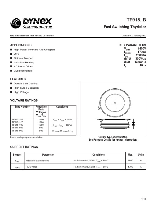
APPLICATIONSs High Power Inverters And Choppers s UPSs Railway Traction s Induction Heating s AC Motor Drives s CycloconvertersFEATURESs Double Side Cooling s High Surge Capability s High VoltageVOLTAGE RATINGSKEY PARAMETERSV DRM 1400V I T(RMS)1700A I TSM 20000A dV/dt 300V/µs dI/dt 500A/µs t q 40µsConditionsV RSM = V RRM + 100V I DRM = I RRM = 60mA at V RRM or V DRM & T vjRepetitivePeak Voltages V DRM V RRMType Number140012001000800600Lower voltage grades available.TF915 14B TF915 12B TF915 10B TF915 08B TF915 06BOutline type code: MU169.See Package Details for further information.CURRENT RATINGSParameterConditionsMax.Units Mean on-state current RMS valueHalf sinewave, 50Hz, T case = 80o C Half sinewave, 50Hz, T case = 80o C10801700A ASymbol I T(AV)I T(RMS)TF915..BFast Switching ThyristorReplaces December 1998 version, DS4279-3.0DS4279-4.0 January 2000SURGE RATINGSParameterConditionsMax.Units I 2t for fusing10ms half sine; V R = 0% V RRM , T j = 125˚C 20.0kA A 2sSurge (non-repetitive) on-state current 10ms half sine; V R = 0% V RRM , T j = 125˚CSymbol I TSM I 2t2000 x 103THERMAL AND MECHANICAL DATAdc ConditionsMin.Max.UnitsoC/W --Anode dcClamping force 23.5kN with mounting compound Thermal resistance - case to heatsinkR th(c-h)0.006Double side -125oC T vj Virtual junction temperatureT stg Storage temperature range Reverse (blocking)Single side-Thermal resistance - junction to caseR th(j-c)Single side cooledSymbolParameterClamping force22.324.6kN-40150oC-On-state (conducting)-125oC-0.012oC/WoC/W Cathode dc--oC/W Double side cooled-0.020oC/WMEASUREMENT OF RECOVERED CHARGE - QRA1DYNAMIC CHARACTERISTICSV TM ParameterSymbol ConditionsMaximum on-state voltage At 2000A peak, T case = 25o C I RRM /I DRM Peak reverse and off-state current At V RRM /V DRM , T case = 125o CGate source 20V, 20Ωt r ≤ 0.5µs, T j = 125˚CdV/dtMaximum linear rate of rise of off-state voltageLinear to 60% V DRM T j = 125o C, Gate open circuit Min.Max.Units - 1.75V -60mA -300V/µs Repetitive 50Hz-500A/µsNon-repetitive-800A/µs Rate of rise of on-state currentdI/dtV T(TO)Threshold voltage At T vj = 125o C r T On-state slope resistance At T vj = 125o C1.25-V -0.25m ΩDelay time t gd 1.5*-µs Total turn-on time t (ON)TOT3.0*-µs T j = 25˚C, I T = 50A,V D = 300V, I G = 1A,dI/dt = 50A/µs, dI G /dt = 1A/µs *Typical value.I H Holding current T j = 25o C, I TM = 1A, V D = 12V 100*-mA T j = 125˚C, I T = 250A, V R = 50V,dV/dt = 20V/µs (Linear to 60% V DRM ),dI R /dt = 50A/µs, Gate open circuitTurn-off timet q40-µst q code: B GATE TRIGGER CHARACTERISTICS AND RATINGSV DRM = 12V, T case = 25o C, R L = 6ΩConditionsParameterSymbol V GT Gate trigger voltage V DRM = 12V, T case = 25o C, R L = 6ΩI GT Gate trigger current V GD Gate non-trigger voltage At V DRM T case = 125o C, R L = 1k Ω- 3.0V -200mA -0.2V Typ.Max.Units V RGM Peak reverse gate voltage I FGM Peak forward gate current Anode positive with respect to cathodeP GM Peak gate power P G(AV)Mean gate power- 5.0V -10A -50W -3WI L Latching currentT j = 25o C, I G = 0.5A, V D = 12V300*-mACURVESNOTES:1. V D ≤ 600V.2. V R ≤ 10V.3. R.C Snubber, C = 0.22µF, R =4.7ΩNOTES:1. V D ≤ 600V.2. V R ≤ 10V.3. R.C Snubber, C = 0.22µF, R =4.7ΩNOTES:1. V D ≤ 600V.2. V R ≤ 10V.3. R.C Snubber, C = 0.22µF, R =4.7ΩNOTES:1. dI/dt = 25A/µs2. V D ≤ 600V.3. V R ≤ 10V.4. R.C Snubber, C = 0.22µF, R = 4.7ΩNOTES:1. dI/dt = 25A/µs2. V D ≤ 600V.3. V R ≤ 10V.4. R.C Snubber, C = 0.22µF, R = 4.7ΩNOTES:1. dI/dt = 25A/µs2. V D ≤ 600V.3. V R ≤ 10V.4. R.C Snubber, C = 0.22µF, R = 4.7ΩNOTES:1. dI/dt = 50A/µs2. V D ≤ 600V.3. V R ≤ 10V.4. R.C Snubber, C = 0.22µF, R = 4.7ΩNOTES:1. dI/dt = 50A/µs2. V D ≤ 600V.3. V R ≤ 10V.4. R.C Snubber, C = 0.22µF, R = 4.7ΩNOTES:1. dI/dt = 50A/µs2. V D ≤ 600V.3. V R ≤ 10V.4. R.C Snubber, C = 0.22µF, R = 4.7ΩNOTES:1. dI/dt = 100A/µs2. V D ≤ 600V.3. V R ≤ 10V.4. R.C Snubber, C = 0.22µF, R = 4.7ΩTF915..B11/13NOTES:1. dI/dt = 100A/µs2. V D ≤ 600V.3. V R ≤ 10V.4. R.C Snubber, C = 0.22µF, R = 4.7ΩNOTES:1. dI/dt = 100A/µs2. V D ≤ 600V.3. V R ≤ 10V.4. R.C Snubber, C = 0.22µF, R = 4.7ΩTF915..B12/13PACKAGE DETAILSFor further package information, please contact your local Customer Service Centre. All dimensions in mm, unless stated otherwise.DO NOT SCALE.ASSOCIATED PUBLICATIONSTitleApplication NoteNumber Calculating the junction temperature or power semiconductors AN4506Gate triggering and the use of gate characteristics AN4840Recommendations for clamping power semiconductors AN4839The effect of temperature on thyristor performance AN4870Thyristor and diode measurement with a multi-meter AN4853Turn-on performance of thyristors in parallel AN4999Use of V TO, r Ton-state characteristicAN5001TF915..B13/13CUSTOMER SERVICE CENTRESFrance, Benelux, Italy and Spain T el: +33 (0)1 69 18 90 00. Fax: +33 (0)1 64 46 54 50North America T el: 011-800-5554-5554. Fax: 011-800-5444-5444UK, Germany, Scandinavia & Rest Of World T el: +44 (0)1522 500500. Fax: +44 (0)1522 500020SALES OFFICESFrance, Benelux, Italy and Spain T el: +33 (0)1 69 18 90 00. Fax: +33 (0)1 64 46 54 50Germany T el: 07351 827723North America T el: (613) 723-7035. Fax: (613) 723-1518. T oll Free: 1.888.33.DYNEX (39639) /T el: (831) 440-1988. Fax: (831) 440-1989 / Tel: (949) 733-3005. Fax: (949) 733-2986.UK, Germany, Scandinavia & Rest Of World Tel: +44 (0)1522 500500. Fax: +44 (0)1522 500020These offices are supported by Representatives and Distributors in many countries world-wide.© Dynex Semiconductor 2000 Publication No. DSxxxx-y Issue No. x.x January 2000TECHNICAL DOCUMENTATION – NOT FOR RESALE. PRINTED IN UNITED KINGDOMHEADQUARTERS OPERATIONS DYNEX SEMICONDUCTOR LTD Doddington Road, Lincoln.Lincolnshire. LN6 3LF. United Kingdom.Tel: 00-44-(0)1522-500500Fax: 00-44-(0)1522-500550DYNEX POWER INC.Unit 7 - 58 Antares Drive,Nepean, Ontario, Canada K2E 7W6.T el: 613.723.7035Fax: 613.723.1518T oll Free: 1.888.33.DYNEX (39639)This publication is issued to provide information only which (unless agreed by the Company in writing) may not be used, applied or reproduced for any purpose nor form part of any order or contract nor to be regarded as a representation relating to the products or services concerned. No warranty or guarantee express or implied is made regarding the capability, performance or suitability of any product or service. The Company reserves the right to alter without prior notice the specification, design or price of any product or service. Information concerning possible methods of use is provided as a guide only and does not constitute any guarantee that such methods of use will be satisfactory in a specific piece of equipment. It is the user's responsibility to fully determine the performance and suitability of any equipment using such information and to ensure that any publication or data used is up to date and has not been superseded. These products are not suitable for use in any medical products whose failure to perform may result in significant injuryor death to the user. All products and materials are sold and services provided subject to the Company's conditions of sale, which are available on request.All brand names and product names used in this publication are trademarks, registered trademarks or trade names of their respective owners.e-mail: power_solutions@Datasheet Annotations:Dynex Semiconductor annotate datasheets in the top right hard corner of the front page, to indicate product status. The annotations are as follows:-Target Information: This is the most tentative form of information and represents a very preliminary specification. No actual design work on the product has been started.Preliminary Information: The product is in design and development. The datasheet represents the product as it is understood but details may change.Advance Information: The product design is complete and final characterisation for volume production is well in hand.No Annotation: The product parameters are fixed and the product is available to datasheet specification.POWER ASSEMBLY CAPABILITYThe Power Assembly group was set up to provide a support service for those customers requiring more than the basic semiconduc-tor, and has developed a flexible range of heatsink / clamping systems in line with advances in device types and the voltage and current capability of our semiconductors.We offer an extensive range of air and liquid cooled assemblies covering the full range of circuit designs in general use today. The Assembly group continues to offer high quality engineering support dedicated to designing new units to satisfy the growing needs of our customers.Using the up to date CAD methods our team of design and applications engineers aim to provide the Power Assembly Complete solution (PACs).DEVICE CLAMPSDisc devices require the correct clamping force to ensure their safe operation. The PACs range offers a varied selection of pre-loaded clamps to suit all of our manufactured devices. This include cube clamps for single side cooling of ‘T’ 22mm Clamps are available for single or double side cooling, with high insulation versions for high voltage assemblies.Please refer to our application note on device clamping, AN4839HEATSINKSPower Assembly has it’s own proprietary range of extruded aluminium heatsinks. They have been designed to optimise theperformance or our semiconductors. Data with respect to air natural, forced air and liquid cooling (with flow rates) is available on request.For further information on device clamps, heatsinks and assemblies, please contact your nearest Sales Representative or the factory.。
