NTE225中文资料
2SK1522中文资料(renesas)中文数据手册「EasyDatasheet - 矽搜」

7.如果这些产品或技术受日本出口管理限制,必须是 日本政府根据许可证出口,不能导入比批准目地以外国家.
禁止任何转移或再出口违反出口管制法律和日本及/或目地国家相关规定.
8.请与瑞萨科技公司对这些材料或产品进一步详情 其中所载.
芯片中文手册,看全文,戳
V GS = ±25 V, V DS = 0 V DS = 360 V, V GS = 0 V DS = 400 V, V GS = 0 ID =1毫安,V DS = 10 V ID = 25 A, V GS = 10 V * 1
ID = 25 A, V DS = 10 V * 1 VDS = 10 V, V GS = 0, F = 1兆赫
芯片中文手册,看全文,戳
2SK1521, 2SK1522
绝对最大额定值
(Ta = 25°C)
项目
漏极至源极电压
2SK1521
2SK1522
门源电压
漏极电流
漏电流峰值
身体流失二极管反向漏电流
频道耗散
通道温度
储存温度
注:1.PW
10 µs, 占空比
1%
2.价值在T C = 25°C
符号
ID = 25 A, V GS = 10 V, RL = 1.2
IF = 50 A, V GS = 0
IF = 50 A, V GS = 0, di F/ DT = 100 A /μs的
3
—
远期转移导纳
|yfs|
22
输入电容
Ciss —
输出电容
Coss —
反向传输电容
Crss —
导通延迟时间 上升时间 关断延迟时间 下降时间 身体向前漏二极管 电压
NTE215中文资料
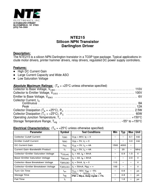
V(BR)CEO IC = 50mA, RBE = ∞
元器件交易网
Schematic Diagram
C B
ELeabharlann .190 (4.82).615 (15.62)
C .787 (20.0)
.591 (15.02)
.126 (3.22) Dia
.787 (20.0)
B
C
E
.215 (5.47)
元器件交易网
NTE215 Silicon NPN Transistor Darlington Driver
Description: The NTE215 is a silicon NPN Darlington transistor in a TO3P type package. Typical applications include motor drivers, printer hammer drivers, relay drivers, regulated DC power supply controllers. Features: D High DC Current Gain D Large Current Capacity and Wide ASO D Low Saturation Voltage Absolute Maximum Ratings: (TA = +25°C unless otherwise specified) Collector to Base Voltage, VCBO . . . . . . . . . . . . . . . . . . . . . . . . . . . . . . . . . . . . . . . . . . . . . . . . . . . . . 110V Collector to Emitter Voltage, VCEO . . . . . . . . . . . . . . . . . . . . . . . . . . . . . . . . . . . . . . . . . . . . . . . . . . . 100V Emitter to Base Voltage, VEBO . . . . . . . . . . . . . . . . . . . . . . . . . . . . . . . . . . . . . . . . . . . . . . . . . . . . . . . . 6V Collector Current, IC Continuous . . . . . . . . . . . . . . . . . . . . . . . . . . . . . . . . . . . . . . . . . . . . . . . . . . . . . . . . . . . . . . . . . . . 8A Peak . . . . . . . . . . . . . . . . . . . . . . . . . . . . . . . . . . . . . . . . . . . . . . . . . . . . . . . . . . . . . . . . . . . . . . . 12A Collector Dissipation (TA = +25°C), PC . . . . . . . . . . . . . . . . . . . . . . . . . . . . . . . . . . . . . . . . . . . . . . . 2.5W Collector Dissipation (TC = +25°C), PC . . . . . . . . . . . . . . . . . . . . . . . . . . . . . . . . . . . . . . . . . . . . . . 60W Operating Junction Temperature, TJ . . . . . . . . . . . . . . . . . . . . . . . . . . . . . . . . . . . . . . . . . . . . . . . +150°C Storage Temperature Range, Tstg . . . . . . . . . . . . . . . . . . . . . . . . . . . . . . . . . . . . . . . . . . –55° to +150°C Electrical Characteristics: (TA = +25°C unless otherwise specified)
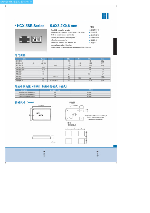
E5SB25.0000F12E33中文资料(Hosonic)中文数据手册「EasyDatasheet - 矽搜」
1.6 1.35 0.7 1.35
电气规格
参数 频率范围
25频率公差
温度稳定性 工作温度范围 存储温度范围 并联电容 负载电容 绝缘电阻 驱动电平
Aging(at 25 )
Symb
FO F /佛 TC TOP R
TS T G CO CL IR DL
Fa
况
25
100VDC 在25℃,每年
Min
Typ
Max
Units
12
48
MHz
10
30
芯片中文手册,看全文,戳
HCX-5SB Series
5.0X3.2X0.8 mm
特征
The 5SB crystal is an ultra miniature packagewith size of 5.0X3.2X0.8mm. With its ceramicbase and metal
超微型尺寸 行业标准 频率范围宽
cover it provides the durabilityand reliability necessary for strenuous process like infrared and
Seam weld
浮雕录音 回流焊
vapor phase reflow. Excellent performance for application in wireless communication.
Mode
基本的 基本的 基本的
机械尺寸(mm)
5.00 0.20
标记
3.20 0.20
AREA
0.8 0.1
顶视图
2.30 0.10 1.20
4
3
0.85
6MBI225U-120中文资料
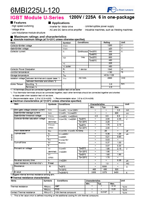
6MBI225U-1201200V / 225A 6 in one-packageFeatures· High speed switching· Voltage drive· Low inductance module structureApplications · Inverter for Motor drive· AC and DC Servo drive amplifierMaximum ratings and characteristicsThermal resistance characteristicsThermal resistanceContact Thermal resistance––0.12––0.20–0.0167 –IGBTFWDWith thermal compound°C/W°C/W°C/W*2 : Two thermistor terminals should be connected together, each other terminals should be connected together and shortedto base plate when isolation test will be done.*3 :Recommendable value : 2.5 to 3.5 N·m(M5) *4 :Recommendable value : 3.5 to 4.5 N·m(M6)Rth(j-c)Rth(j-c)Rth(c-f)*5IGBT Module U-Series*5 : This is the value which is defined mounting on the additional cooling fin with thermal compound.4Items Symbols Conditions Characteristics UnitMin.Typ. Max.· Uninterruptible power supply· Industrial machines, such as Welding machinesCharacteristics (Representative)VGE=0V, f= 1MHz, Tj= 25°CVcc=600V, I=225A, Tj= 25°CCollector current vs. Collector-Emitter voltage (typ.)Tj= 125°C / chipCapacitance vs. Collector-Emitter voltage (typ.)Dynamic Gate charge (typ.)Collector current vs. Collector-Emitter voltage (typ.)Tj= 25°C / chipCollector current vs. Collector-Emitter voltage (typ.)VGE=15V / chipTj=25°C / chipCollector-Emitter voltage vs. Gate-Emitter voltage (typ.)010020030040050060012345C o l l e c t o r c u r r e n t : I c [A ]VGE=20V15V12V10V8V010020030040050060012345C o l l e c t o r c u r r e n t : I c [A ]VGE=20V 15V12V10V8V010020030040050060001234C o l l e c t o r c u r r e n t : I c [A ]Tj=125°CTj=25°C246810510152025C o l l e c t o r - E m i t t e r v o l t a g e : V C E [ V ]Ic=450A Ic=225A Ic= 112.5A0.11.010.0100.0102030C a p a c i t a n c e : C i e s , C o e s , C r e s [ n F ]200400600800100012001400C o l l e c t o r -E m i t t e r v o l t a g e : V C E [ 200V /d i v ]G a t e - E m i t t e r v o l t a g e : V G E [ 5V /d i v]Vcc=600V, Ic=225A, VGE=±15V, Tj= 25°CStray inductance <= 100nHSwitching loss vs. Collector current (typ.)Vcc=600V, VGE=±15V, Rg=3ΩVcc=600V, Ic=225A, VGE=±15V, Tj= 125°C+VGE=15V,-VGE <= 15V, RG >= 3Ω ,Tj <= 125°CSwitching time vs. Collector current (typ.)Vcc=600V, VGE=±15V, Rg=3Ω, Tj=125°CSwitching time vs. Gate resistance (typ.)Switching time vs. Collector current (typ.)Vcc=600V, VGE=±15V, Rg=3Ω, Tj= 25°CReverse bias safe operating area (max.)Switching loss vs. Gate resistance (typ.)10100100010000100200300400S w i t c h i n g t i m e : t o n , t r , t o f f , t f [ n s e c ]Collector current : Ic [ A ]10100100010000100200300400S w i t c h i n g t i m e : t o n , t r , t o f f , t f [ n s e c ]Collector current : Ic [ A ]10100100010000110100S w i t c h i n g t i m e : t o n , t r , t o f f , t f [ n s e c ]Gate resistance : Rg [ Ω ]trtftoffton 01020304050100200300400500S w i t c h i n g l o s s : E o n , E o f f , E r r [ m J /p u l s e ]Collector current : Ic [ A ]Eon(125°C)Eon(25°C)Eoff(125°C)Err(125°C)Err(25°C)Eoff(25°C)0255075100125150110100S w i t c h i n g l o s s : E o n , E o f f , E r r [ m J /p u l s e ]Gate resistance : Rg [ Ω ]EoffErrEon0100200300400500600200400600800100012001400C o l l e c t o r c u r r e n t : I c [ A ]Collector - Emitter voltage : VCE [ V ]Transient thermal resistance (max.)Reverse recovery characteristics (typ.)Vcc=600V, VGE=±15V, Rg=3ΩForward current vs. Forward on voltage (typ.)chipTemperature characteristic (typ.)01002003004005006001234F o r w a r d c u r r e n t : I F [ A ]Forward on voltage : VF [ V ]Tj=125°CTj=25°C101001000100200300400500R e v e r s e r e c o v e r y c u r r e n t : I r r [ A ]R e v e r s e r e c o v e r y t i m e : t r r [ n s e c ]Forward current : IF [ A ]Irr (125°C)Irr (25°C)trr (125°C)trr (25°C)0.0010.0100.1001.0000.0010.0100.1001.000T h e r m a l r e s i s t a n s e : R t h (j -c ) [ °C /W ]Pulse width : Pw [ sec ]0.1110100-60-40-20020406080100120140160180Temperature [°C ]R e s i s t a n c e : R [ k Ω ]Outline Drawings, mmM6296MBI225U-120IGBT ModuleEquivalent Circuit Schematic[Thermister]135111210987246[Inverter]。
2STR2215;中文规格书,Datasheet资料

c shows exceptional high gain performances du coupled with very low saturation voltage. Obsolete Pro The complementary NPN is the 2STR1215.
Date
Revision
Changes
09-Feb-2006
1
Initial release.
20-Jul-2006
2
New template.
08-Sep-2008
3
Updated the SOT-23 mechanical data.
Updated Figure 1: Internal schematic diagram
Produc hFE (1) DC current gain
IC = -50 mA VCE = -2 V 200
IC = -500 mA VCE = -2 V 200 280 560
IC = -1 A IC = -2 A
VCE = -2 V 130 VCE = -2 V 80
leteCCBO
Collector-base capacitance (IE = 0)
IEBO
(IC =0)
VEB = -4 V
-0.1 µA
) Collector-base
t(s V(BR)CBO breakdown voltage
IC = -100 µA
-15
V
c (IE = 0)
rodu V(BR)CEO (1)
Collector-emitter breakdown voltage
USR2-T220中文资料
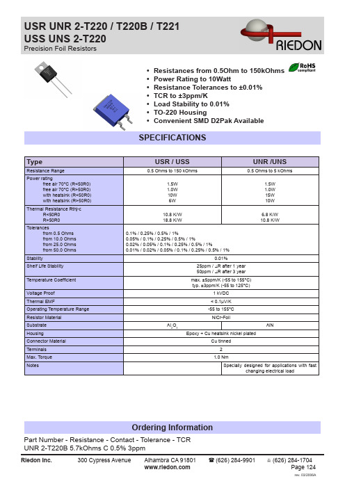
UNR /UNS
0.5 Ohms to 5 kOhms 1.5W 1.0W 15W 10W 6.8 K/W 10.8 K/W
AlN
Ordering Information
Part Number - Resistance - Contact - Tolerance - TCR UNR 2-T220B 5.7kOhms C 0.5% 3ppm
USR UNR 2-T220 / T220B / T221 USS UNS 2-T220
Precision Foil Resistors SPECIFICATIONS (continued) Dimensions
Dimension mm 17.30 10.16 6.00 Ø3.7 16.40 5.08 0.76 1.30 10.00 13.80 2.00 1.20 4.00 2.90 0.40 1.85 tol. (±mm) 0.2 0.2 0.1 0.1 0.2 0.1 0.1 0.1 0.2 0.2 0.1 0.1 0.1 0.1 0.1 0.1 tol. (±mm) 0.2 0.2 0.1 0.1 0.2 0.1 0.1 0.1 0.2 0.2 0.1 0.1 0.1 0.1 0.1 0.1 inches 0.68 0.40 0.24 Ø0.146 0.65 0.20 0.03 0.05 0.39 0.54 0.08 0.05 0.16 0.11 0.02 0.07 tol. (±inches) 0.008 0.008 0.004 0.004 0.008 0.004 0.004 0.004 0.008 0.008 0.004 0.004 0.004 0.004 0.004 0.004 tol. (±inches) 0.008 0.008 0.004 0.004 0.008 0.004 0.004 0.004 0.008 0.008 0.004 0.004 0.004 0.004 0.004 0.004
PT2262、PT2272 编码解码芯片中文资料
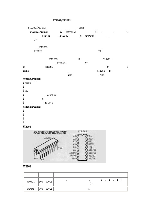
PT2262/PT2272编码解码芯片中文资料PT2262/PT2272是台湾普城公司生产的一种CMOS工艺制造的低功耗低价位通用编解码电路,PT2262/PT2272最多可有12位(A0-A11)三态地址端管脚(悬空,接高电平,接低电平),任意组合可提供531441地址码,PT2262最多可有6位(D0-D5)数据端管脚,设定的地址码和数据码从17脚串行输出,可用于无线遥控发射电路。
编码芯片PT2262发出的编码信号由:地址码、数据码、同步码组成一个完整的码字,解码芯片PT2272接收到信号后,其地址码经过两次比较核对后,VT脚才输出高电平,与此同时相应的数据脚也输出高电平,如果发送端一直按住按键,编码芯片也会连续发射。
当发射机没有按键按下时,PT2262不接通电源,其17脚为低电平,所以315MHz的高频发射电路不工作,当有按键按下时,PT2262得电工作,其第17脚输出经调制的串行数据信号,当17脚为高电平期间315MHz的高频发射电路起振并发射等幅高频信号,当17脚为低平期间3 15MHz的高频发射电路停止振荡,所以高频发射电路完全收控于PT2262的17脚输出的数字信号,从而对高频电路完成幅度键控(ASK调制)相当于调制度为100%的调幅。
PT2262/PT2272特点l CMOS工艺制造,低功耗l 外部元器件少l RC振荡电阻l 工作电压范围宽:2.6-15vl 数据最多可达6位l 地址码最多可达531441种PT2262/PT2272应用范围l 车辆防盗系统l 家庭防盗系统l 遥控玩具l 其他电器遥控PT2262 引脚图:PT2262管脚说明:名称管脚说明A0-A11 1-8、10-13 地址管脚,用于进行地址编码,可置为“0”,“1”,“f”(悬空),D0-D5 7-8、10-13 数据输入端,有一个为“1”即有编码发出,内部下拉Vcc 18 电源正端(+)Vss 9 电源负端(-)TE 14 编码启动端,用于多数据的编码发射,低电平有效;OSC1 16 振荡电阻输入端,与OSC2所接电阻决定振荡频率;OSC2 15 振荡电阻振荡器输出端;Dout 17 编码输出端(正常时为低电平)在具体的应用中,外接振荡电阻可根据需要进行适当的调节,阻值越大振荡频率越慢,编码的宽度越大,发码一帧的时间越长.PT2262参数PT2272 解码电路引脚图:名称管脚说明A0-A11 1-8、10-13 地址管脚,用于进行地址编码,可置为“0”,“1”,“f”(悬空),必须与2262一致,否则不解码D0-D5 7-8、10-13 地址或数据管脚,当做为数据管脚时,只有在地址码与2262一致,数据管脚才能输出与2262数据端对应的高电平,否则输出为低电平,锁存型只有在接收到下一数据才能转换Vcc 18 电源正端(+)Vss 9 电源负端(-)DIN 14 数据信号输入端,来自接收模块输出端OSC1 16 振荡电阻输入端,与OSC2所接电阻决定振荡频率;OSC2 15 振荡电阻振荡器输出端;VT 17解码有效确认输出端(常低)解码有效变成高电平(瞬态)PT2272解码芯片有不同的后缀,表示不同的功能,有L4/M4/L6/M6之分,其中L表示锁存输出,数据只要成功接收就能一直保持对应的电平状态,直到下次遥控数据发生变化时改变。
HI1-0222-5中文资料

Applications
• Routing Switchers • Production Mixers • High Definition TV • Radar Signal Conditioning
• Medical Imaging • Heads-Up Displays • Simulators • Sonar
3 2 1 20 19
GND 4 NC 5 V+ 6 NC 7 NC 8
18 VA1 17 NC 16 V15 NC 14 VA2 9 10 11 12 13
V-
Q
LEVEL SHIFTER AND
V+
Q
DRIVER
V-
LOGIC INPUT
VIN2 NC NC
VOUT2 NC
NOTE: Source and Drain are arbitrarily depicted as Analog Input and Output, respectively. They may be interchanged without affecting performance. All nonconnected pins should be tied to ground.
Crosstalk and off isolation are optimized with a T-switch configuration and the use of nonconnected pins for extended shielding. Other features of the HI-222 include wideband operation, low rON, fast switching speeds and low differential gain and phase. The characteristics of this TTL compatible device make it ideal for designs where improved switching performance is required.
2SJ352中文资料

2SJ352中⽂资料2SJ351, 2SJ352Silicon P-Channel MOS FETADE-208-1431st. EditionApplicationLow frequency power amplifierComplementary pair with 2SK2220, 2SK2221FeaturesHigh power gainExcellent frequency responseHigh speed switchingWide area of safe operationEnhancement-modeGood complementary characteristicsEquipped with gate protection diodesOrdering InformationType No.VDSX2SJ351–180 V2SJ352–200 V2SJ351, 2SJ3522OutlineAbsolute Maximum Ratings (Ta = 25°C)ItemSymbol Ratings Unit Drain to source voltage 2SJ351V DSX–180V2SJ352–200Gate to source voltage V GSS ±20V Drain currentI D –8A Body to drain diode reverse drain current I DR –8A Channel dissipation Pch*1100W Channel temperature Tch 150°C Storage temperature Tstg –55 to +150°C Note:1.Value at T C = 25°C2SJ351, 2SJ3523Electrical Characteristics (Ta = 25°C)ItemSymbol Min Typ Max Unit Test conditions Drain to source 2SJ351V (BR)DSX–180——VI D = –10 mA, V GS = 10 Vbreakdown voltage2SJ352–200——Gate to source breakdown voltageV (BR)GSS ±20——V I G = ±100 µA, V DS = 0Gate to source cutoff voltage V GS(off)–0.15—–1.45V I D = –100 mA, V DS =–10 V Drain to source saturation voltageV DS(sat)——–12V I D = –8 A, V GD = 0*1Forward transfer admittance |y fs |0.7 1.0 1.4S I D = –3 A, V DS = –10 V*1Input capacitance Ciss —800—pF V GS = 5 V, V DS = –10 V,Output capacitanceCoss —1000—pF f = 1 MHzReverse transfer capacitance Crss —18—pF Turn-on time t on —320—ns V DD = –30 V, I D = –4 A Turn-off time t off—120—nsNote:1.Pulse test2SJ351, 2SJ35242SJ351, 2SJ3526Hitachi CodeJEDECEIAJWeight (reference value)TO-3P—Conforms5.0 gUnit: mmCautions1.Hitachi neither warrants nor grants licenses of any rights of Hitachi’s or any third party’s patent,copyright, trademark, or other intellectual property rights for information contained in this document.Hitachi bears no responsibility for problems that may arise with third party’s rights, includingintellectual property rights, in connection with use of the information contained in this document.2.Products and product specifications may be subject to change without notice. Confirm that you have received the latest product standards or specifications before final design, purchase or use.3.Hitachi makes every attempt to ensure that its products are of high quality and reliability. However,contact Hitachi’s sales office before using the product in an application that demands especially high quality and reliability or where its failure or malfunction may directly threaten human life or cause risk of bodily injury, such as aerospace, aeronautics, nuclear power, combustion control, transportation,traffic, safety equipment or medical equipment for life support.4.Design your application so that the product is used within the ranges guaranteed by Hitachi particularly for maximum rating, operating supply voltage range, heat radiation characteristics, installationconditions and other characteristics. Hitachi bears no responsibility for failure or damage when used beyond the guaranteed ranges. Even within the guaranteed ranges, consider normally foreseeable failure rates or failure modes in semiconductor devices and employ systemic measures such as fail-safes, so that the equipment incorporating Hitachi product does not cause bodily injury, fire or other consequential damage due to operation of the Hitachi product.5.This product is not designed to be radiation resistant.6.No one is permitted to reproduce or duplicate, in any form, the whole or part of this document without written approval from Hitachi.7.Contact Hitachi’s sales office for any questions regarding this document or Hitachi semiconductor products.Hitachi, Ltd.Semiconductor & Integrated Circuits.Nippon Bldg., 2-6-2, Ohte-machi, Chiyoda-ku, Tokyo 100-0004, Japan Tel: Tokyo (03) 3270-2111 Fax: (03) 3270-5109 Copyright ' Hitachi, Ltd., 1999. All rights reserved. Printed in Japan.Hitachi Asia Pte. Ltd.16 Collyer Quay #20-00Hitachi TowerSingapore 049318Tel: 535-2100Fax: 535-1533URLNorthAmerica : http:/doc/bfe7be20915f804d2b16c12b.html /Europe :/doc/bfe7be20915f804d2b16c12b.html /hel/ecg Asia (Singapore):/doc/bfe7be20915f804d2b16c12b.html .sg/grp3/sicd/index.htm Asia (Taiwan):/doc/bfe7be20915f804d2b16c12b.html /E/Product/SICD_Frame.htm Asia (HongKong):/doc/bfe7be20915f804d2b16c12b.html /eng/bo/grp3/index.htm Japan :http://www.hitachi.co.jp/Sicd/indx.htmHitachi Asia Ltd.Taipei Branch Office3F, Hung Kuo Building. No.167, Tun-Hwa North Road, Taipei (105)Tel: <886> (2) 2718-3666Fax: <886> (2) 2718-8180 Hitachi Asia (Hong Kong) Ltd.Group III (Electronic Components)7/F., North Tower, World Finance Centre,Harbour City, Canton Road, Tsim Sha Tsui,Kowloon, Hong Kong Tel: <852> (2) 735 9218Fax: <852> (2) 730 0281 Telex: 40815 HITEC HXHitachi Europe Ltd.Electronic Components Group.Whitebrook ParkLower Cookham Road MaidenheadBerkshire SL6 8YA, United Kingdom Tel: <44> (1628) 585000Fax: <44> (1628) 778322Hitachi Europe GmbHElectronic components Group Dornacher Stra§e 3D-85622 Feldkirchen, Munich GermanyTel: <49> (89) 9 9180-0Fax: <49> (89) 9 29 30 00Hitachi Semiconductor (America) Inc.179 East Tasman Drive,San Jose,CA 95134 Tel: <1> (408) 433-1990Fax: <1>(408) 433-0223For further information write to:。
NTJD2152PT1;NTJD2152PT1G;NTJD2152PT2;NTJD2152PT2G;NTJD2152PT4;中文规格书,Datasheet资料
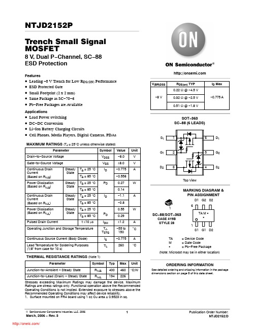
NTJD2152PTrench Small Signal MOSFET8 V, Dual P−Channel, SC−88ESD ProtectionFeatures•Leading –8 V Trench for Low R DS(ON) Performance •ESD Protected Gate•Small Footprint (2 x 2 mm)•Same Package as SC−70−6•Pb−Free Packages are AvailableApplications•Load Power switching•DC−DC Conversion•Li−Ion Battery Charging Circuits•Cell Phones, Media Players, Digital Cameras, PDAs MAXIMUM RATINGS (T J= 25°C unless otherwise stated)Parameter Symbol Value Unit Drain−to−Source Voltage V DSS−8.0V Gate−to−Source Voltage V GS±8.0VContinuous Drain Current (Based on R q JA)SteadyStateT A = 25 °CI D−0.775AT A = 85 °C−0.558Power Dissipation (Based on R q JA)SteadyStateT A = 25 °C P D0.27WT A = 85 °C0.14Continuous Drain Current (Based on R q JL)SteadyStateT A = 25 °C I D−1.1AT A = 85 °C−0.8Power Dissipation (Based on R q JL)SteadyStateT A = 25 °CP D0.55W T A = 85 °C0.29Pulsed Drain Current t ≤10 m s I DM±1.2AOperating Junction and Storage Temperature T J,T STG −55 to150°CContinuous Source Current (Body Diode)I S−0.775A Lead Temperature for Soldering Purposes(1/8” from case for 10 s)T L260°C THERMAL RESISTANCE RATINGS(Note 1)Parameter Symbol Typ Max Unit Junction−to−Ambient – Steady State R q JA400460°C/W Junction−to−Lead (Drain) – Steady State R q JL194226 Stresses exceeding Maximum Ratings may damage the device. Maximum Ratings are stress ratings only. Functional operation above the Recommended Operating Conditions is not implied. Extended exposure to stresses above the Recommended Operating Conditions may affect device reliability.1.Surface mounted on FR4 board using 1 oz Cu area = 0.9523 in sq.V(BR)DSS R DS(on) TYP I D Max−8 V0.22 W @ −4.5 V0.32 W @ −2.5 V0.51 W @ −1.8 V−0.775 ASee detailed ordering and shipping information in the package dimensions section on page 5 of this data sheet.ORDERING INFORMATIONELECTRICAL CHARACTERISTICS (T J=25°C unless otherwise stated)Parameter Symbol Test Condition Min Typ Max Unit OFF CHARACTERISTICSDrain−to−Source Breakdown Voltage V(BR)DSS V GS= 0 V, I D= −250 m A−8.0−10.5VDrain−to−Source Breakdown Voltage Temperature Coefficient V(BR)DSS/T J−6.0mV/°CZero Gate Voltage Drain Current I DSS V GS= 0 V, V DS= −6.4V 1.0m A Gate−to−Source Leakage Current I GSS V DS= 0 V, V GS= ±8.0V10m A ON CHARACTERISTICS (Note 2)Gate Threshold Voltage V GS(TH)V GS= V DS, ID = −250 m A−0.45−0.83−1.0V Gate Threshold TemperatureCoefficientV GS(TH)/T J 2.2mV/ °C Drain−to−Source On Resistance R DS(on)V GS= −4.5V, I D= −0.57A0.220.3WV GS= −2.5V, I D= −0.48A0.320.46V GS = −1.8V, I D= −0.20A0.510.9Forward Transconductance g FS V GS= −4.0V, I D= −0.57A 2.0S CHARGES AND CAPACITANCESInput Capacitance C ISS V GS= 0 V, f = 1.0 MHz,V DS= −8.0V 160225pFOutput Capacitance C OSS3855 Reverse Transfer Capacitance C RSS2840Total Gate Charge Q G(TOT)V GS= −4.5 V, V DS= −5.0V,I D= −0.6A 2.2 4.0nCThreshold Gate Charge Q G(TH)0.1 Gate−to−Source Charge Q GS0.5 Gate−to−Drain Charge Q GD0.5 SWITCHING CHARACTERISTICS (Note 3)Turn−On Delay Time td(ON)V GS= −4.5V, V DD= −4.0V,I D= −0.5A, R G= 8.0 W 13nsRise Time tr23 Turn−Off Delay Time td(OFF)50 Fall Time tf36 DRAIN−SOURCE DIODE CHARACTERISTICSForward Diode Voltage V SD V GS= 0 V,I S= −0.23A T J= 25°C0.76 1.1V T J= 125°C0.63Reverse Recovery Time t RR V GS= 0 V, dI S/dt = 100 A/m s,I S= −0.77A78ns2.Pulse Test: pulse width ≤ 300m s, duty cycle ≤ 2%.3.Switching characteristics are independent of operating junction temperatures.−I D , D R A I N C U R R E N T (A M P S )0.10.30.20R D S (o n ), D R A I N −T O −S O U R C E R E S I S T A N C E (W )Figure 5. On −Resistance Variation withTemperatureT J , JUNCTION TEMPERATURE (°C)0.5R D S (o n ), D R A I N −T O −S O U R C E R E S I S T A N C E (N O R M A L I Z E D )Figure 6. Capacitance Variation0.4GATE −TO −SOURCE OR DRAIN −TO −SOURCEVOLTAGE (VOLTS)Figure 7. Gate −to −Source andDrain −to −Source Voltage vs. Total Charge1.2Figure 8. Diode Forward Voltage vs. CurrentQ g , TOTAL GATE CHARGE (nC)−V G S , G A T E −T O −S O U R C E V O L T A G E (V O L T S )21.60.80.42.40.80.10−V SD , SOURCE −TO −DRAIN VOLTAGE (VOLTS)−I S , S O U R C E C U R R E N T (A M P S )0.70.60.40.40.50.60.20.310.2ORDERING INFORMATIONDevice Order Number Package Type Tape and Reel Size†NTJD2152PT1SOT−3633000 / Tape & Reel3000 / Tape & ReelNTJD2152PT1G SOT−363(Pb−Free)NTJD2152PT2SOT−3633000 / Tape & Reel3000 / Tape & ReelNTJD2152PT2G SOT−363(Pb−Free)NTJD2152PT4SOT−36310,000 / Tape & Reel10,000 / Tape & ReelNTJD2152PT4G SOT−363(Pb−Free)†For information on tape and reel specifications, including part orientation and tape sizes, please refer to our T ape and Reel Packaging Specifi-cations Brochure, BRD8011/D.PACKAGE DIMENSIONSNOTES:1.DIMENSIONING AND TOLERANCING PER ANSI Y14.5M, 1982.2.CONTROLLING DIMENSION: INCH.3.419B −01 OBSOLETE, NEW STANDARD 419B −02.SC −88/SC70−6/SOT −363CASE 419B −02ISSUE WDIM MIN NOM MAX MILLIMETERS A 0.800.95 1.10A10.000.050.10A3b 0.100.210.30C 0.100.140.25D 1.80 2.00 2.200.0310.0370.0430.0000.0020.0040.0040.0080.0120.0040.0050.0100.0700.0780.086MIN NOM MAX INCHES0.20 REF 0.008 REFH EE 1.15 1.25 1.35e 0.65 BSC L 0.100.200.302.00 2.10 2.200.0450.0490.0530.026 BSC0.0040.0080.0120.0780.0820.086*For additional information on our Pb −Free strategy and solderingdetails, please download the ON Semiconductor Soldering and Mounting Techniques Reference Manual, SOLDERRM/D.STYLE 26:PIN 1.SOURCE 12.GATE 13.DRAIN 24.SOURCE 25.GATE 26.DRAIN 1ON Semiconductor and are registered trademarks of Semiconductor Components Industries, LLC (SCILLC). SCILLC reserves the right to make changes without further notice to any products herein. SCILLC makes no warranty, representation or guarantee regarding the suitability of its products for any particular purpose, nor does SCILLC assume any liability arising out of the application or use of any product or circuit, and specifically disclaims any and all liability, including without limitation special, consequential or incidental damages.“Typical” parameters which may be provided in SCILLC data sheets and/or specifications can and do vary in different applications and actual performance may vary over time. All operating parameters, including “Typicals” must be validated for each customer application by customer’s technical experts. SCILLC does not convey any license under its patent rights nor the rights of others. SCILLC products are not designed, intended, or authorized for use as components in systems intended for surgical implant into the body, or other applications intended to support or sustain life, or for any other application in which the failure of the SCILLC product could create a situation where personal injury or death may occur. Should Buyer purchase or use SCILLC products for any such unintended or unauthorized application, Buyer shall indemnify and hold SCILLC and its officers, employees, subsidiaries, affiliates,and distributors harmless against all claims, costs, damages, and expenses, and reasonable attorney fees arising out of, directly or indirectly, any claim of personal injury or death associated with such unintended or unauthorized use, even if such claim alleges that SCILLC was negligent regarding the design or manufacture of the part. SCILLC is an Equal Opportunity/Affirmative Action Employer. This literature is subject to all applicable copyright laws and is not for resale in any manner.PUBLICATION ORDERING INFORMATION分销商库存信息:ONSEMINTJD2152PT1NTJD2152PT1G NTJD2152PT2 NTJD2152PT2G NTJD2152PT4NTJD2152PT4G。
pt2262,2272芯片资料

集成电路PT2262/PT2272编码解码芯片原理简介PT2262/2272是台湾普城公司生产的一种CMOS工艺制造的低功耗低价位通用编解码电路,PT2262/2272最多可有12位(A0-A11)三态地址端管脚(悬空,接高电平,接低电平),任意组合可提供531441地址码,PT2262最多可有6位(D0-D5)数据端管脚,设定的地址码和数据码从17脚串行输出,可用于无线遥控发射电路。
编码芯片PT2262发出的编码信号由:地址码、数据码、同步码组成一个完整的码字,解码芯片PT2272接收到信号后,其地址码经过两次比较核对后,VT脚才输出高电平,与此同时相应的数据脚也输出高电平,如果发送端一直按住按键,编码芯片也会连续发射。
当发射机没有按键按下时,PT2262不接通电源,其17脚为低电平,所以315MHz的高频发射电路不工作,当有按键按下时,PT2262得电工作,其第17脚输出经调制的串行数据信号,当17脚为高电平期间315MHz 的高频发射电路起振并发射等幅高频信号,当17脚为低平期间315MHz的高频发射电路停止振荡,所以高频发射电路完全收控于PT2262的17脚输出的数字信号,从而对高频电路完成幅度键控(ASK 调制)相当于调制度为100%的调幅。
PT2262/2272特点:CMOS工艺制造,低功耗,外部元器件少,RC振荡电阻,工作电压范围宽:2.6~15v,数据最多可达6位,地址码最多可达531441种。
应用范围:车辆防盗系统、家庭防盗系统、遥控玩具、其他电器遥控。
名称管脚说明A0-A1 11-8、10-13地址管脚,用于进行地址编码,可置为“0”,“1”,“f”(悬空),D0-D57-8、10-13数据输入端,有一个为“1”即有编码发出,内部下拉Vcc18电源正端(+)Vss9电源负端(-)TE14编码启动端,用于多数据的编码发射,低电平有效;OSC116振荡电阻输入端,与OSC2所接电阻决定振荡频率;OSC215振荡电阻振荡器输出端;Dout17编码输出端(正常时为低电平)在具体的应用中,外接振荡电阻可根据需要进行适当的调节,阻值越大振荡频率越慢,编码的宽度越大,发码一帧的时间越长。
1N5222B中文资料
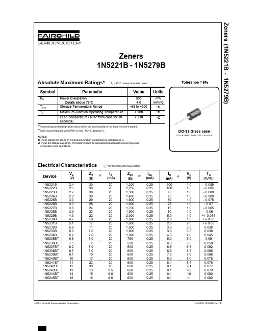
ZZK
(Ω) 600 600 600 600 600 600 600 600 600 600 600 700 700 800 900 1000 1100 1300 1400 1400 1600 1700 2000 2200 2300 2600 3000 4000 4500 4500 5000 5500 5500 6000
SPM™ Stealth™ SuperSOT™-3 SuperSOT™-6 SuperSOT™-8 SyncFET™ TinyLogic TruTranslation™ UHC™ UltraFET VCX™
FAIRCHILD SEMICONDUCTOR RESERVES THE RIGHT TO MAKE CHANGES WITHOUT FURTHER NOTICE TO ANY PRODUCTS HEREIN TO IMPROVE RELIABILITY, FUNCTION OR DESIGN. FAIRCHILD DOES NOT ASSUME ANY LIABILITY ARISING OUT OF THE APPLICATION OR USE OF ANY PRODUCT OR CIRCUIT DESCRIBED HEREIN; NEITHER DOES IT CONVEY ANY LICENSE UNDER ITS PATENT RIGHTS, NOR THE RIGHTS OF OTHERS.
ACEx™ FACT™ ActiveArray™ FACT Quiet Series™ Bottomless™ FAST CoolFET™ FASTr™ CROSSVOLT™ FRFET™ DOME™ GlobalOptoisolator™ EcoSPARK™ GTO™ E2CMOSTM HiSeC™ EnSignaTM I2C™ Across the board. Around the world.™ The Power Franchise™ Programmable Active Droop™
2N7002中文资料(fairchild)中文数据手册「EasyDatasheet - 矽搜」

1995年11月
2N7000 / 2N7002 / NDS7002A N沟道增强型场效应晶体管
概述
这些N沟道增强型场效应晶体管 采用飞兆半导体专有,高密度生产, DMOS技术.这些产品目是为最大限度地减少通态电阻 ,同时提供坚固,可靠和快速开关性能.他们可以在需要高 达400mA DC大多数应用中使用,并且可以提供脉冲电流 高达2A.这些产品特别适用于低电压,低电流应用, 如小伺服电机控制,功率MOSFET栅极驱动器,和其他开关 应用.
V 1 µA 1 mA 1 µA 0.5 mA 10 nA 100 nA
-10 nA -100 nA
V = V , I =1毫安
2N7000 0.8 2.1 3
V
V = V , I = 250 µA
2N7002 1 2.1 2.5 NDS7002A
= 10 V, I =500毫安
2N7000
1.2 5
T =125°C
1.9 9
V = 4.5 V, I =75毫安
1.8 5.3
V = 10 V, I =500毫安
2N7002
1.2 7.5
T =100°C
1.7 13.5
V = 5.0 V, I =50毫安
1.7 7.5
T =100C
2.4 13.5
V = 10 V, I =500毫安
NDS7002 A
V在
VGS
R GEN
G
V DD
RL
D
V出
DUT
S
图 11.
t d(on)
t on tr
90%
t d(of f )
t of f tf
MHV5IC2215NR2;中文规格书,Datasheet资料
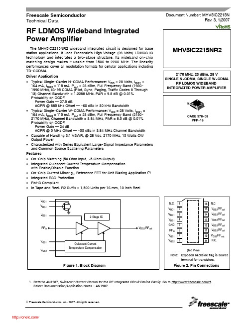
RF LDMOS Wideband Integrated Power AmplifierThe MHV5IC2215NR2 wideband integrated circuit is designed for base station applications. It uses Freescale’s High Voltage (28 Volts) LDMOS IC technology and integrates a two -stage structure. Its wideband on -chip matching design makes it usable from 1500 to 2200 MHz. The linearity performances cover all modulation formats for cellular applications including TD-SCDMA.Driver Application•Typical Single-Carrier N-CDMA Performance: V DD = 28 Volts, I DQ1 = 164 mA, I DQ2 = 115 mA, P out = 23 dBm, Full Frequency Band (1930-1990 MHz), IS-95 CDMA (Pilot, Sync, Paging, Traffic Codes 8 Through 13) Channel Bandwidth = 1.2288 MHz. PAR = 9.8 dB @ 0.01% Probability on CCDF.Power Gain — 27.5 dBACPR @ 885 kHz Offset — -60 dBc in 30 kHz Bandwidth•Typical Single -Carrier W-CDMA Performance: V DD = 28 Volts, I DQ1 = 164 mA, I DQ2 = 115 mA, P out = 23 dBm, Full Frequency Band (2130-2170 MHz), Channel Bandwidth = 3.84 MHz, PAR = 8.5 dB @ 0.01%Probability on CCDF.Power Gain — 24 dBACPR @ 5 MHz Offset — -55 dBc in 3.84 MHz Channel Bandwidth •Capable of Handling 3:1 VSWR, @ 28 Vdc, 2170 MHz, 15 Watts CW Output Power•Characterized with Series Equivalent Large-Signal Impedance Parameters and Common Source Scattering Parameters Features•On-Chip Matching (50 Ohm Input, >5 Ohm Output)•Integrated Quiescent Current Temperature Compensation with Enable/Disable Function•On-Chip Current Mirror g m Reference FET for Self Biasing Application (1)•Integrated ESD Protection •RoHS Compliant•In Tape and Reel. R2 Suffix = 1,500 Units per 16 mm, 13 inch Reel1.Refer to AN1987, Quiescent Current Control for the RF Integrated Circuit Device Family. Go to /rf.Select Documentation/Application Notes - AN1987.Document Number: MHV5IC2215NRev. 3, 1/2007Freescale Semiconductor Technical DataMHV5IC2215NR2Table 1. Maximum RatingsRatingSymbol Value Unit Drain-Source Voltage V DSS -0.5, +65Vdc Gate-Source Voltage V GS -0.5, +12Vdc Storage Temperature Range T stg -65 to +150°C Operating Junction Temperature T J 150°C Input PowerP in12dBmTable 2. Thermal CharacteristicsCharacteristicSymbol Value (1)Unit Thermal Resistance, Junction to Case Driver Application Stage 1, 28 Vdc, I DQ1 = 164 mA (P out = 23 dBm CW)Stage 2, 28 Vdc, I DQ2 = 115 mAR θJC9.33.5°C/WTable 3. ESD Protection CharacteristicsTest MethodologyClass Human Body Model (per JESD22-A114)0 (Minimum)Machine Model (per EIA/JESD22-A115) A (Minimum)Charge Device Model (per JESD22-C101)III (Minimum)Table 4. Moisture Sensitivity LevelTest MethodologyRating Package Peak TemperatureUnit Per JESD 22-A113, IPC/JEDEC J-STD-0203260°CTable 5. Electrical Characteristics (T C = 25°C unless otherwise noted)CharacteristicSymbolMinTypMaxUnitW-CDMA Functional Tests (In Freescale Test Fixture, 50 ohm system) V DD = 28 Vdc, I DQ1 = 164 mA, I DQ2 = 115 mA, P out = 23 dBm, f = 2140 MHz, Single-carrier W-CDMA, 3.84 MHz Channel Bandwidth Carrier. ACPR measured in 3.84 MHz Channel Bandwidth @ ±5 MHz Offset. PAR = 8.5 dB @ 0.01% Probability on CCDF.Power GainG ps 232427dB Gain Flatness in 60 MHz Bandwidth @ P out = 23 dBmf = 2110-2170 MHz G F —0.30.5dB Adjacent Channel Power Ratio ACPR —-56-54dBc Input Return LossIRL—-12-10dBTypical N-CDMA Tests (In Freescale Test Fixture, 50 ohm system) V DD = 28 Vdc, I DQ1 = 164 mA, I DQ2 = 115 mA, P out = 23 dBm, f = 1960 MHz, Single-Carrier N-CDMA, 1.2288 MHz Channel Bandwidth Carrier. ACPR measured in 30 kHz Channel Bandwidth @ ±885 kHz Offset. PAR = 9.8 dB @ 0.01% Probability on CCDF Power GainG ps 25.527.529dB Gain Flatness @ P out = 23 dBm f = 1930-1990 MHzG F —0.3—dB Adjacent Channel Power Ratio ACPR —-60—dBc Input Return LossIRL —-12—dB Average Deviation from Linear Phase in 60 MHz Bandwidth @ P out = 23 dBm Φ—0.2—°Average Group Delay @ P out = 23 dBm Including Output MatchingDelay—1.5—ns1.Refer to AN1955, Thermal Measurement Methodology of RF Power Amplifiers. Go to /rf. Select Documentation/Application Notes - AN1955.MHV5IC2215NR2W-CDMA DRIVER APPLICATIONFigure 3. MHV5IC2215NR2 Test Circuit SchematicV V Z80.0105″ x 0.1200″Microstrip Z90.0559″ x 0.1145″Microstrip Z100.045″ x 0.2671″Microstrip Z110.3319″ x 0.0349″Microstrip Z120.0027″ x 2.0413″Microstrip Z130.9151″ x 0.0349″Microstrip PCBRogers 4350, 0.020″, εr = 3.5Z10.045″ x 0.1289″Microstrip Z20.0443″ x 0.0161″Microstrip Z30.0308″ x 0.0416″x 0.03″Taper Z40.0161″ x 0.0685″Microstrip Z50.0838″ x 0.1759″Microstrip Z60.0503″ x 0.1759″Microstrip Z70.0922″ x 0.1759″Microstrip Table 6. MHV5IC2215NR2 Test Circuit Component Designations and ValuesPartDescriptionPart Number Manufacturer C122 pF, 50 V Chip Capacitor 06033J220GBS AVX C2, C3 6.8 pF, 50 V Chip Capacitors 06035J6R8BBS AVX C4, C7 1 μF, 35 V Tantalum Chip Capacitors TAJA105K035R AVX C5, C6330 μF, 50 V Electrolytic Chip Capacitors MCR35V337M10X16Multicomp C80.01 μF, 50 V Chip Capacitor 0805C103K5RACTR Kemet C9, C10 2.7 pF, 50 V Chip Capacitors 06035J2R7BBS AVX C1115 pF, 25 V Chip Capacitor 06033J150GBS AVX R1, R21 k W , 1/8 W Chip ResistorsCRCW08051000FKTAVishayMHV5IC2215NR2W-CDMA DRIVER APPLICATIONFigure 4. MHV5IC2215NR2 Test Circuit Component LayoutMHV5IC2215NR2TYPICAL W-CDMA DRIVER APPLICATION CHARACTERISTICSI M 3 (d B c ), A C P R (d B c )0−66P out , OUTPUT POWER (WATTS) AVG.33027−1221−2415−363−600.1110−489Figure 5. 2-Carrier W-CDMA ACPR, IM3, PowerGain and Power Added Efficiencyversus Output PowerP A E , P O W E R A D D E D E F F I C I E N C Y (%), G p s , P O W E R G A I N (d B )302418126−6−18−30−42−543018280.1501012624222040302010P out , OUTPUT POWER (WATTS) CWFigure 6. Power Gain and Power AddedEfficiency versus Output PowerG p s , P O W E R G A I N (d B )P A E , P O W E R A D D E D E F F I C I E N C Y (%)P out , OUTPUT POWER (WATTS) CWFigure 7. Power Gain versus Output Power1019268252423202221246G p s , P O W E R G A I N (d B )12143000−21281000−16−2f, FREQUENCY (MHz)Figure 8. Broadband Frequency Response 21−414−67−80−10−7−12−14−14250020001500S 11 (d B )S 21 (d B )23001830190026242220195020502150f, FREQUENCY (MHz)Figure 9. Power Gain versus FrequencyG p s , P O W E R G A I N (d B )282000210022002250MHV5IC2215NR2TYPICAL CHARACTERISTICS250 10990T J, JUNCTION TEMPERATURE (°C)Figure 10. MTTF versus Junction TemperatureThis above graph displays calculated MTTF in hours when the deviceis operated at V DD = 28 Vdc and P out = 23 dBm.MTTF calculator available at http://rf. Select Tools/Software/Application Software/Calculators to access the MTTF calcu−lators by product.108107105110130150170190MTTF(HOURS)210230 106MHV5IC2215NR2Figure 11. Series Equivalent Input and Load Impedance, 2140 MHzVDD = 28 Vdc, I DQ1 = 164 mA, I DQ2 = 115 mA, P out = 23 dBm Z in=Device input impedance as measured from gate to ground.Z load =Test circuit impedance as measuredfrom drain to ground.ZinZloadOutput Matching Networkf MHz Z in ΩZ load Ω211021402170 1.03 - j0.870.94 - j0.350.99 - j0.6175.39 - j12.3971.11 - j18.8366.07 - j22.68Z o = 75 Ωf = 2110 MHzZ inf = 2170 MHzZ loadf = 2170 MHzf = 2110 MHzMHV5IC2215NR2N-CDMA DRIVER APPLICATIONFigure 12. MHV5IC2215NR2 Test Circuit SchematicZ80.0559″ x 0.1145″Microstrip Z90.0450″ x 0.2671″Microstrip Z100.3319″ x 0.0349″Microstrip Z110.0027″ x 2.0413″Microstrip Z120.9151″ x 0.0349″Microstrip PCBRogers 4350, 0.020″, εr = 3.5Z10.045″ x 0.1289″Microstrip Z20.0443″ x 0.0161″Microstrip Z30.0308″ x 0.0416″x 0.03″Taper Z40.0161″ x 0.0685″Microstrip Z50.0838″ x 0.1759″Microstrip Z60.1425″ x 1.7590″Microstrip Z70.0105″ x 0.1200″MicrostripV V Table 7. MHV5IC2215NR2 Test Circuit Component Designations and ValuesPartDescriptionPart Number Manufacturer C122 pF, 25 V Chip Capacitor 06033J220GBS AVX C2, C3 6.8 pF, 50 V Chip Capacitors 06035J6R8BBS AVX C4, C7 1 μF, 35 V Tantalum Chip Capacitors TAJA105K035R AVX C5, C6330 μF, 50 V Electrolytic Chip Capacitors MCR35V337M10X16Multicomp C80.01 μF, 50 V Chip Capacitor 0805C103K5RACTR Kemet C9, C10 2.4 pF, 50 V Chip Capacitors 06035J2R4BBS AVX C1115 pF, 25 V Chip Capacitor 06033J150GBS AVX C12 1.5 pF, 50 V Chip Capacitor 06035J1R5BBS AVX R1, R21 k W , 1/8 W Chip ResistorsCRCW08051000FKTAVishayN-CDMA DRIVER APPLICATIONFigure 13. MHV5IC2215NR2 Test Circuit Component LayoutMHV5IC2215NR2MHV5IC2215NR2TYPICAL N-CDMA DRIVER APPLICATION CHARACTERISTICSIM3(dBc),ACPR(dBc)0−66P out, OUTPUT POWER (WATTS) AVG.44036−1228−2420−364−600.1110−4812Figure 14. 2-Carrier N-CDMA ACPR, IM3, PowerGain and Power Added Efficiencyversus Output PowerPAE,POWERADDEDEFFICIENCY(%),Gps,POWERGAIN(dB)403224168−6−18−30−42−543026310.1501013029282740302010P out, OUTPUT POWER (WATTS) CWFigure 15. Power Gain and Power AddedEfficiency versus Output PowerGps,POWERGAIN(dB)PAE,POWERADDEDEFFICIENCY(%)3000−24321000−16−2f, FREQUENCY (MHz)Figure 16. Broadband Frequency Response24−416−68−80−10−8−12−16−14250020001500S11(dB)S21(dB)分销商库存信息: FREESCALEMHV5IC2215NR2。
NTF2955T1中文资料
NTF2955T1中⽂资料NTF2955Power MOSFET60 V, 2.6 A, Single PChannel SOT223 FeaturesTMOS7 Design for low R DS(on)Withstands High Energy in Avalanche and Commutation Modes ApplicationsPower SuppliesPWM Motor ControlConvertersPower ManagementMAXIMUM RATINGS (T= 25°C unless otherwise noted)THERMAL RESISTANCE RATINGSMaximum ratings applied to the device are individual stress limit values (not normal operating conditions) and are not valid simultaneously. If these limits are exceeded, device functional operation is not implied, damage may occur and reliability may be affected.1.When surface mounted to an FR4 board using 1 in. pad size(Cu. area = 1.127 in2 [1 oz] including traces)2.When surface mounted to an FR4 board using the minimum recommendedpad size (Cu. area = 0.341 in2)/doc/b917194021.htmlDevice Package Shipping?ORDERING INFORMATIONNTF2955T1SOT?2231000/T ape & ReelGate Drain SourceNTF2955T3SOT?2234000/T ape & ReelFor information on tape and reel specifications, including part orientation and tape sizes, please refer to our Tape and Reel Packaging Specification Brochure, BRD8011/D.(T=25°C unless otherwise stated)OFF CHARACTERISTICSON CHARACTERISTICS (Note 3)CHARGES AND CAPACITANCESSWITCHING CHARACTERISTICS (Note 4)DRAIN?SOURCE DIODE CHARACTERISTICS3.Pulse Test: pulse width ≤ 300m s, duty cycle ≤ 2%.4.Switching characteristics are independent of operating junction temperatures.Figure 5. On?Resistance Variation withTemperatureFigure 6. Drain?to?Source Leakage Currentversus VoltageR D S (o n ), D R A I N ?T O ?S O U R C E R E S I S T A N C E (?)T J , JUNCTION TEMPERATURE (°C)R D S (o n ), D R A I N ?T O ?S O U R C E R E S I S T A N C E (N O R M A L I Z E D ) 5050252575125100150V DS, DRAINTOSOURCE VOLTAGE (VOLTS)5406030201050?I D , D R A I N C U R R E N T (A M P S )4535251555C , C A P A C I T A N C E (p F ))t , T I M E (n s )Figure 11. Maximum Rated Forward BiasedSafe Operating Area ?V DS , DRAIN?TO?SOURCE VOLTAGE (VOLTS)Figure 12. Maximum Avalanche Energy versus Starting Junction TemperatureT J , STARTING JUNCTION TEMPERATURE (°C)I D , D R A I N C U R R E N T (A M P S )E VPACKAGE DIMENSIONSSTYLE 3:PIN 1.GATE 2.DRAIN 3.SOURCE 4.DRAINDIM A MIN MAX MIN MAX MILLIMETERS 0.2490.263 6.30 6.70INCHESB 0.1300.145 3.30 3.70C 0.0600.068 1.50 1.75D 0.0240.0350.600.89F 0.1150.126 2.90 3.20G 0.0870.094 2.20 2.40H 0.00080.00400.0200.100J 0.0090.0140.240.35K0.0600.078 1.50 2.00L 0.0330.0410.85 1.05M 0 10 0 10 S 0.2640.287 6.707.30NOTES:1.DIMENSIONING AND TOLERANCING PER ANSI Y14.5M, 1982.2.CONTROLLING DIMENSION: INCH.____SOT?223 (TO?261)CASE 318E?04ISSUE KSOLDERING FOOTPRINTON Semiconductor and are registered trademarks of Semiconductor Components Industries, LLC (SCILLC). SCILLC reserves the right to make changes without further notice to any products herein. SCILLC makes no warranty, representation or guarantee regarding the suitability of its products for any particular purpose, nor does SCILLC assume any liability arising out of the application or use of any product or circuit, and specifically disclaims any and all liability, including without limitation special, consequential or incidental damages.“Typical” parameters which may be provided in SCILLC data sheets and/or specifications can and do vary in different applications and actual performance may vary over time. All operating parameters, including “Typicals” must be validated for each customer application by customer’s technical experts. SCILLC does not convey any license under its patent rights nor the rights of others. SCILLC products are not designed, intended, or authorized for use as components in systems intended for surgical implant into the body, or other applications intended to support or sustain life, or for any other application in which the failure of the SCILLC product could create a situation where personal injury or death may occur. Should Buyer purchase or use SCILLC products for any such unintended or unauthorized application, Buyer shall indemnify and hold SCILLC and its officers, employees, subsidiaries, affiliates, and distributors harmless against all claims, costs, damages, and expenses, and reasonable attorney fees arising out of, directly or indirectly, any claim of personal injury or death associated with such unintended or unauthorized use, even if such claim alleges that SCILLC was negligent regarding the design or manufacture of the part. SCILLC is an Equal Opportunity/Affirmative Action Employer. This literature is subject to all applicable copyright laws and is not for resale in any manner.PUBLICATION ORDERING INFORMATION。
大众热成型标准中文翻译TL4225_EN
无涂层和预涂层的合金淬火回火钢22MnB5对半成品及零部件的材料要求TL4225(2006-05-01)关键词:淬火回火钢,22MnB5,冲压淬火,感应淬火,预涂,铝硅热浸镀涂层,板材,冷轧,热轧,管变化以下变化是与技术供应规范TL4225(1995-09)相比做出的,标准全面修订1.范围此标准对基体为22MnB5,通过冲压淬火或者感应淬火做出的无涂层或者预涂层热轧或者冷轧钢板、钢管(厚度0.65~6.00mm)进行了要求。
2.说明冲压淬火金属板的说明案例是由冷轧制造的厚度1.5mm的无涂层原材料:材质:TL4225+C半成品:EN10131-1,5冲压淬火Al-Si涂层钢板的说明案例是一种厚度为2.0mm,涂层重量为150g/m2(DIN EN 10292标准涂层):材质:TL4225+AS150半成品:EN10143-2,0焊接钢管的说明案例是一种外径为30mm厚度为3.0mm,一种无涂层通过感应淬火(水淬)墙强化的材料:材质:TL4225钢管:30×3.0-EN10305-33.制造方法见表1。
表14.要求4.1基本要求首要供应的批准和变化是根据大众标准VW01155。
禁止的有害物质是根据大众标准VW91101。
4.2化学成分(wt%)见表2。
4.3对未强化板材和管材的要去4.3.1机械性能根据标准DIN EN 10002-1确定垂直于轧制方向的机械性能,根据标准DIN50125试样尺寸H20×80,这和不带涂层的试样横截面有关。
见表3-板材原材料机械性能。
4.3.2基体在冷轧条件下,基体组织为铁素体、珠光体和碳化物沉淀,并且偶尔含有小部分的贝氏体。
典型晶粒大小>10 ASTM,见图1.除非批准,否则有明显边界的锰硫化物并且沿纵向排列长度大于50 µm 是不允许的,见图2。
偏离基体要求需要获得负责质量保证部门的批准。
图1 在未硬化条件下基体组织(横向微区,放大倍数500倍)图2 拉长的锰硫化物>50 µm(横向微区,未腐蚀,500倍)4.3.3表面和涂层的要求4.3.3.1未腐蚀板冷轧产品初始条件下表面状态根据DIN EN 10268。
- 1、下载文档前请自行甄别文档内容的完整性,平台不提供额外的编辑、内容补充、找答案等附加服务。
- 2、"仅部分预览"的文档,不可在线预览部分如存在完整性等问题,可反馈申请退款(可完整预览的文档不适用该条件!)。
- 3、如文档侵犯您的权益,请联系客服反馈,我们会尽快为您处理(人工客服工作时间:9:00-18:30)。
NTE225
Silicon NPN Transistor
Linear Amplifier and High Speed Switch
Description:
The NTE225 is a silicon NPN transistor in a TO39 type package (with flange) designed for industrial and commercial equipment. Typical applications include high voltage differential and operational am-plifiers, high voltage inverters, and high voltage, low current switching and series regulators. Features:
D High Voltage Rating: V CEO(sus) = 350V Max.
D Low Saturation Voltage
Absolute Maximum Ratings:
Collector−Base Voltage, V CBO450V
. . . . . . . . . . . . . . . . . . . . . . . . . . . . . . . . . . . . . . . . . . . . . . . . . . . . . .
. . . . . . . . . . . . . . . . . . . . . . . . . . . . . . . . . . . . . . . Collector−Emitter Sustaining Voltage, V CEO(sus)350V
. . . . . . . . . . . . . . . . . . . . . . . . . . . . . . . . . . . . . . . . . . . . . . . . . . . . . . . . . . Emitter−Base Voltage, V EBO7V . . . . . . . . . . . . . . . . . . . . . . . . . . . . . . . . . . . . . . . . . . . . . . . . . . . . . . . . . . . . . . . . . Collector Current, I C1A . . . . . . . . . . . . . . . . . . . . . . . . . . . . . . . . . . . . . . . . . . . . . . . . . . . . . . . . . . . . . . . .
Base Current, I B500mA
. . . . . . . . . . . . . . . . . . . . . . . . . . . . . . . . . . . . . . . . . . . . Total Power Dissipation (T C = +25°C), P D10W Operating Junction Temperature Range, T J−65° to +200°C
. . . . . . . . . . . . . . . . . . . . . . . . . . . . . . . . . .
. . . . . . . . . . . . . . . . . . . . . . . . . . . . . . . . . . . . . . . . . .
Storage Temperature Range, T stg−65° to +200°C
. . . . . . . . . . . . . . . . . . . . . . . . . . . . . . . . . . . . Thermal Resistance, Junction−to−Case, R thJC17.5°C/W Lead Temperature (During Soldering, 1/32” from seating plane for 10sec Max, T L+255°C
. . . . . . . Electrical Characteristics: (T C = +25°C unless otherwise specified)
Parameter Symbol Test Conditions Min Typ Max Unit Collector−Emitter Sustaining Voltage V CEO(sus)I C = 50mA, I B = 0, Base Open, Note 1350−−V Collector Cutoff Current I CEO V CE = 300V, I B = 0−−20µA
I CEV V CE = 450V, V BE = −1.5V−−500µA Emitter Cutoff Current I EBO V BE = 6V, I C = 0−−20µA DC Current Gain h FE V CE = 10V, I C = 20mA40−160
V CE = 10V, I C = 2mA30−−Collector−Emitter Saturation Voltage V CE(sat)I C = 50mA, I B = 4mA−−0.5V Base−Emitter Saturation Voltage V BE(sat)I C = 50mA, I B = 4mA−− 1.3V Small−Signal Current Gain h fe V CE = 10V, I C = 10mA, f = 5MHz3−−
Output Capacitance C ob V CB = 10V, I E = 0, f = 1MHz−−10pF Second Breakdown Collector Current I S/b V CE = 200V, with Base Forward Biased50−−mA Note 1.The sustaining voltage (V CEO(sus)) MUST NOT be measured on a curve tracer.。
