MAX5026EUT+T中文资料
JW5026 中文数据手册
JW502616路恒流LED驱动器版本 作者 日期 更改描述 V1.0 2010.12 16路恒流LED驱动器1 一、概述JW5026是一款高性能LED恒流驱动芯片,芯片采用最新的半导体技术,专为LED显示面板提供驱动。
芯片包括CMOS移位寄存器电路和锁存电路,将串行输入的数据转换成并行的16路LED恒流输出。
JW5026有16个恒流电源,可以为每个输出级提供5~90mA的恒流驱动。
JW5026驱动电流大小可以通过调节外接调节电阻来调整,通过此机制使用者可以轻松的控制LED的发光亮度。
JW5026的设计保证其输出级颗耐压17V以上,因此可以在每个输出端串接多个LED。
JW5026可以支持25MHZ的高时钟频率以满足系统对大量数据传输上的要求。
JW5026具有良好的芯片串接性能,能支持大量芯片在高时钟频率下的串接使用。
JW5026具有精确的电流输出值,通道间最大差异值<±3%,不同芯片间的最大差异值<±5%。
JW5026采用具有散热功能的SSOP24封装,保证芯片在大电流工作条件下的稳定工作。
二、特性说明◆ 16路等电流输出通道◆ 等电流输出值不受输出端负载电压的影响◆ 精确的电流输出值:通道间最大差异值<±3%,不同芯片间的最大差异值<±5%◆ 通过外接电阻,方便的调节输出电流的大小◆ 快速的输出电流响应,输出使能端的最小值可达180ns◆ 等电流输出范围可达5~90mA◆ 支持高达25MHZ的时钟频率◆ 芯片输出端可耐压17V,支持多个LED显示灯串联◆ 采用施密特触发器对输入数据进行锁存◆ 芯片工作电压5V三、芯片功能框图图1 JW5026 芯片功能框图四、引脚定义图2 JW5026-SSOP24NO 名称 输入/出功能1 GND IN 控制逻辑及驱动电流的接地端2 SDI IN 输入到移位寄存器的串行数据输入端3 CLK IN 时钟信号,数据移位发生在时钟的上升沿4LE IN 数据闪控(data strobe)输入控制端当LE为高电平是,串行数据会被传入至输出锁存器;当LE为低电平时,资料会被锁存5-20 IN 等电流输出端3 21IN输出使能信号端当为低电平时,启动输出 当为高电平时,关闭输出22 SDO OUT 串行数据输出端23 R-EXT IN 外接电流调节电阻输入端,通过改变此电阻的值,可以设定所有输出通道的输出电流大小 24 VDDIN5V 电源供电端五、输入输出等效电路图3 JW5026输入输出端等效电路4六、芯片功能时序图图4 JW5026功能时序七、真值表5八、最大工作范围特性代表符号最大工作范围单位 电源电压 Vdd 0~7 V 输入端电压 Vin -0.4~Vdd+0.4V 输出端电流 Iout +60 mA 输出端电压 Vds -0.5~+17 V 时钟频率 Fclk 25 MHZ 接地端电流 Ignd 1260 mA 消耗功耗 Pd TBD W 热阻值 Rth(j-a)TBD ℃/W 工作环境温度 Topr -40~+85 ℃ 储存环境温度Tstg-55~+150℃九、直流特性测试电路图5 JW5026直流特性测试电路6十、交流特性测试电路图6 JW5026交流特性测试电路 十一、直流特性特性 代表符号 测量条件 最小值一般值最大值单位电源电压 Vdd 4.5 5.0 5.5 V输出端电压 Vds 18 V Iout 直流特性测试电路 5 60 mAIOH SDO -1.0 mA 输出端电流IOL SDO 1.0 mA高电位值 VIH 0.8Vdd Vdd V输入端电压 低电位值VIL GND0.3VddV输出端漏电流 IOH VOH =17V 0.5 uA VOL IOL = 1 mA 0.4 V 输出端电压 SDOVOHIOH = -1 mA4.5 V输出电流1 Iout1 VDS=0.7VRext=88321.40 mA电流偏移值 d Iout1 VDS=0.7VRext=883Iout = 21.40mA±1±2.5%输出电流2 Iout2 VDS=1.1V 46.01mA7Rext=410电流偏移值 d Iout2VDS=1.1VRext=883 Iout =46.10mA±1.5 ±2.5%电流偏移值VS 输出电压 %/dVDS 输出电压=1.0~3.0V ±0.1%/V 电流偏移值VS 电源电压 %/dVDD 电源电压=4.5~5.5V±0.05%/VPull-up 电阻Rin(up)250 500800 Pull-down 电阻 Rin(down) LE250500800 Idd(off)1 Rext=∞,3.82Idd (off )2 Rext =720, 6.71 OFFIdd (off )3Rext =360,9.99 Idd (on )1 6.07电压源输出电流ONIdd (on )29.32mA十二、交流特性特性代表符号 测量条件最小值一般值 最大值 单位 TpLH1 50 55 80 nsTpLH2 55 70 85 ns TpLH3 70122 129 ns 延迟时间(低电位到高电位) TpLH 29 ns TpHL1 50 55.2 80 ns TpHL2 56 70 86 ns TpHL3 114 124 142 ns 延迟时间(高电位到低电位)TpHL 24 ns CLKTw(CLK) 20 ns LETw(L) 20 ns 脉波宽度Tw(OE) 200 ns LE 的hold time Th(L) 18 ns LE 的setup time Tsu(L) 64 ns SDI 的hold time Th(D) 60 ns SDI 的setup time Tsu(D) VDD=5VVDS=1V VIH=VDD VIL=GND REXT=300VL=4V RL=52 CL=10pF20 ns 时钟频率Fclk IC 串联操作 25 MHZ CLK 信号最大上升时间 Tr 500 ns CLK 信号最大下降时间Tf500 ns 输出电流电位上升时间(note) Tor130ns8输出电流电位下降时间(note) Tof40nsNote:此测试数据只有一路输出电流十三、时序波形图图7 交流特性时序波形图十四、等电流输出通道间的最大电流差异小于±3%,片间电流差异小于±6%,且输出电流大小不受负载端电压影响。
MBI5026 Datasheet-VA.02-CN
量以驱动 LED。
在应用MBI5026于LED面板系统设计之时,MBI5026可提供系统设计人员极大的弹性与极佳的组件效能。
MBI5026的使用者可以经由选用不同阻值的外接电阻器来调整 MBI5026各输出级的电流大小,藉此机制,使用者可轻松地控制LED的发光亮度。
MBI5026的设计保证其输出级可耐压17伏特以上,因此可以在每个输出端串接多个LED。
此外,MBI5026亦提供25MHz的高时钟频率以满足系统对大量数据传输上的需求。
聚积科技2006
台湾新竹市埔顶路18号6F之四
电话:+886-3-579-0068,传真:+886-3-579-7534 E-mail: info@
MBI5026CN\GN轮廓图示MBI5026CNS\GNS轮廓图示
使用权声明
聚积科技对于产品、文件以及服务保有一切变更、修正、修改、改善、以及终止的权利,针对上述的权利,聚积科技不会进行事前预告。
客户在进行产品购买前,建议与聚积科技业务代表联络以取得最新的产品信息。
聚积科技的产品,除非经过聚积合法授权,否则不应使用于医疗或军事行为上,若使用者因此导致任何身体伤害或生命威胁甚至死亡,聚积科技将不负任何损害赔偿责任。
此份文件上所有的文字内容、图片、及商标为聚积科技所属之智慧财产。
除非是先经过聚积合法授权,任何人不得径自使用、修改、重制、公开、改作、散布、发行、公开发表。
如有违反,您应对聚积科技股份有限公司负责损害赔偿责任及其它法律责任。
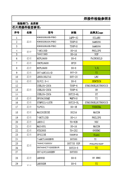
焊接件丝印参照表
107
芯片 LM4040DIM3-2.5
108
芯片 S818A33AMC
109
芯片 74HC4052D
110
ISMB5934BT3
111
B0505LS-1W
DC 模块
24PIN-QEN SOT-23 5PIN SO-16 2PIN
b0505ls
MORNSUN SILABS
TI SII NXP
MICRODC
SO-8
MAXIM
87
芯片 74HC14D
14PIN
NXP
88
芯片 AD8628ART
5PIN
AD
89
芯片 IRF7416
8PIN
IRF
90
芯片 AD712JR
SO-8
ADI
91
芯片 ADUM1400CRW
16PIN
AD
92
芯片 MAX1680
8PIN
MAXIM
93
芯片 TL431ACDBZR
SOT-23
8PIN
166
芯片 OP2347
8PIN
167
芯片 OPA2227
8PIN
168
芯片 TL061
8PIN
169
芯片 ADM101E
10PIN
170
芯片 TPS76950DBVT
5PIN
171
芯片 TPS76350
5PIN
172
芯片 C8051F064
100PIN
173
C8051F069
174
芯片 OPA350
ALTERA
69
芯片 IS62WV5128BLL-55H1I
爱讯通25对大对数线缆
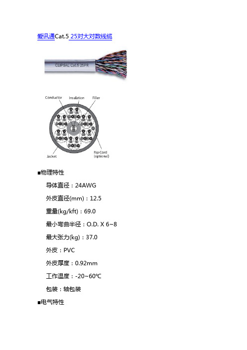
爱讯通Cat.5 25对大对数线缆
■物理特性
导体直径:24AWG
外皮直径(mm):12.5
重量(kg/kft):69.0
最小弯曲半径:O.D. X 6~8
最大张力(kg):37.0
外皮:PVC
外皮厚度:0.92mm
工作温度:-20~60℃
包装:轴包装
■电气特性
阻抗:100欧姆+/-15
静电电容,Max:17.1nf/每千英尺
直流电阻,Max:9..386欧姆/每100米
线对不平衡直流电阻,Max:5%
不平衡电容,Max(线对与地):330pf /100米
传播延迟偏差:45纳秒/100米
额定传输速率:65%
■应用范围
10兆以太网
100兆快速以太网
100VG-AnyLAN
令牌环网
依赖双绞线介质传输模式
100Mbps铜缆分布数据接口
ATM155
语音系统
■符合标准
ISO/IEC-11801
EN-50173
TIA/EIA-568A
总结:爱讯通在超五类网线(cat5e cable),六类网线(cat6 cable),网络跳线,铜包银网线,网络配线架,lan cable,有着9年的网线厂家生产工艺和技术。
MAX5026EUT中文资料
MAX5026EUTRev. ARELIABILITY REPORTFORMAX5026EUTPLASTIC ENCAPSULATED DEVICESMarch 12, 2003MAXIM INTEGRATED PRODUCTS120 SAN GABRIEL DR.SUNNYVALE, CA 94086Written byReviewed byJim Pedicord Bryan J. Preeshl Quality Assurance Quality Assurance Reliability Lab Manager Executive DirectorConclusionThe MAX5026 successfully meets the quality and reliability standards required of all Maxim products. In addition, Maxim’s continuous reliability monitoring program ensures that all outgoing product will continue to meet Maxim’s quality and reliability standards.Table of ContentsI. ........Device Description V. ........Quality Assurance InformationII. ........Manufacturing Information VI. .......Reliability EvaluationIII. .......Packaging Information IV. .......Die Information.....AttachmentsI. Device DescriptionA. GeneralThe MAX5026 constant-frequency, pulse-width modulating (PWM), low-noise boost converter is intended for low-voltage systems that often need a locally generated high voltage. This device is capable of generating low-noise, high output voltages required for varactor diode biasing in TV tuners, set-top boxes, and PCI cable modems. TheMAX5026 operates from as low as 3V and switches at 500kHz.The constant-frequency, current-mode PWM architecture provides for low output noise that is easy to filter. A 40V lateral DMOS device is used as the internal power switch, making the devices ideal for boost converters up to 36V.The MAX5026 adjustable version requires the use of external feedback resistors to set the output voltage.B. Absolute Maximum RatingsItem RatingVCC to GND -0.3V to +12VPGND to GND -0.1V to +0.1VFB to GND -0.3V to (VCC + 0.3V)SHDN to GND -0.3V to (VCC + 0.3V)LX to GND -0.3V to +45VPeak LX Current 600mAOperating Temperature Range -40°C to +85°CJunction Temperature +150°CStorage Temperature Range -65°C to +165°CLead Temperature (soldering 10s) +300°CContinuous Power Dissipation (TA = +70C)6-PIN SOT23 696mWDerates above +70°C6-PIN SOT23 7.1mW/°CII. Manufacturing InformationA. Description/Function: 500kHz, 36V Output, SOT23, PWM Step-Up DC-DC ConvertersB. Process: BCD80C. Number of Device Transistors: 365D. Fabrication Location: Oregon, USAE. Assembly Location: MalaysiaF. Date of Initial Production: April, 2001III. Packaging InformationA. Package Type: 6-Pin SOT23B. Lead Frame: CopperC. Lead Finish: Solder PlateD. Die Attach: Non-Conductive EpoxyE. Bondwire: Gold (1 mil dia.)F. Mold Material: Epoxy with silica fillerG. Assembly Diagram: # 05-1301-0024H. Flammability Rating: Class UL94-V0I. Classification of Moisture Sensitivityper JEDEC standard JESD22-112: Level 1IV. Die InformationA. Dimensions: 60 X 41 milsB. Passivation: Si3N4/SiO2 (Silicon nitride/ Silicon dioxide)C. Interconnect: Aluminum/Si (Si = 1%)D. Backside Metallization: NoneE. Minimum Metal Width: 3 microns (as drawn)F. Minimum Metal Spacing: 3 microns (as drawn)G. Bondpad Dimensions: 5 mil. Sq.H. Isolation Dielectric: SiO2I. Die Separation Method: Wafer SawV. Quality Assurance InformationA. Quality Assurance Contacts: Jim Pedicord (Reliability Lab Manager)Bryan Preeshl (Executive Director)Kenneth Huening (Vice President)B. Outgoing Inspection Level: 0.1% for all electrical parameters guaranteed by the Datasheet.0.1% For all Visual Defects.C. Observed Outgoing Defect Rate: < 50 ppmD. Sampling Plan: Mil-Std-105DVI. Reliability EvaluationA. Accelerated Life TestThe results of the 135°C biased (static) life test are shown in Table 1. Using these results, the Failure Rate (λ) is calculated as follows:λ = 1 = 1.83 (Chi square value for MTTF upper limit)MTTFλ = 15.51 x 10⁻⁹λ = 15.51 F.I.T. (60% confidence level @ 25°C)This low failure rate represents data collected from Maxim’s reliability monitor program. In addition to routine production Burn-In, Maxim pulls a sample from every fabrication process three times per week and subjects it to an extended Burn-In prior to shipment to ensure its reliability. The reliability control level for each lot to be shipped as standard product is 59 F.I.T. at a 60% confidence level, which equates to 3 failures in an 80 piece sample. Maxim performs failure analysis o n any lot that exceeds this reliability control level. Attached Burn-In Schematic (Spec. # 06-5729)shows the static Burn-In circuit. Maxim also performs quarterly 1000 hour life test monitors. This data is published in the Product Reliability Report (RR-1M).B. Moisture Resistance TestsMaxim pulls pressure pot samples from every assembly process three times per week. Each lot sample must meet an LTPD = 20 or less before shipment as standard product. Additionally, the industry standard 85°C/85%RH testing is done per generic device/package family once a quarter.C. E.S.D. and Latch-Up TestingThe NP15die type has been found to have all pins able to withstand a transient pulse of ±2000V, per Mil-Std-883 Method 3015 (reference attached ESD Test Circuit). Latch-Up testing has shown that this device withstands a current of ±250mA.Table 1Reliability Evaluation Test ResultsMAX5026EUTTEST ITEM TEST CONDITION FAILURE SAMPLE NUMBER OFIDENTIFICATION PACKAGE SIZE FAILURES Static Life Test (Note 1)Ta = 135°C DC Parameters 70 0Biased & functionalityTime = 192 hrs.Moisture Testing (Note 2)Pressure Pot Ta = 121°C DC Parameters SOT23 77 0P = 15 psi. & functionalityRH= 100%Time = 168hrs.85/85 Ta = 85°C DC Parameters 77 0RH = 85% & functionalityBiasedTime = 1000hrs.Mechanical Stress (Note 2)Temperature -65°C/150°C DC Parameters 77 0Cycle 1000 Cycles & functionalityMethod 1010Note 1: Life Test Data may represent plastic DIP qualification lots.Note 2: Generic Package/Process dataAttachment #1TABLE II. Pin combination to be tested. 1/ 2/1/ Table II is restated in narrative form in 3.4 below. 2/ No connects are not to be tested. 3/ Repeat pin combination I for each named Power supply and for ground (e.g., where V PS1 is V DD , V CC , V SS , V BB , GND, +V S, -V S , V REF , etc). 3.4 Pin combinations to be tested. a.Each pin individually connected to terminal A with respect to the device ground pin(s) connected to terminal B. All pins except the one being tested and the ground pin(s) shall be open. b. Each pin individually connected to terminal A with respect to each different set of a combination of all named power supply pins (e.g., V SS1, or V SS2 or V SS3 or V CC1, or V CC2) connected to terminal B. All pins except the one being tested and the power supply pin or set of pins shall be open.c.Each input and each output individually connected to terminal A with respect to a combination of all the other input and output pins connected to terminal B. All pins except the input or output pin being tested and the combination of all the other input and output pins shall be open.Terminal A (Each pin individually connected to terminal A with the other floating) Terminal B (The common combination of all like-named pins connected to terminal B) 1. All pins except V PS1 3/ All V PS1 pins 2. All input and output pinsAll other input-output pinsMil Std 883DMethod 3015.7Notice 8TERMINAL BTERMINAL APROBE(NOTE 6) R = 1.5k Ω C = 100pf。
MAX6025AEUR-T中文资料
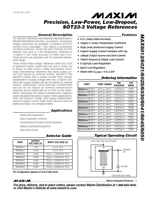
General DescriptionThe MAX6012/MAX6021/MAX6025/MAX6030/MAX6041/MAX6045/MAX6050 precision, low-dropout, micropower voltage references are available in miniature SOT23-3surface-mount packages. They feature a proprietary curvature-correction circuit and laser-trimmed thin-film resistors that result in a low temperature coefficient of <15ppm/°C and initial accuracy of better than 0.2%.These devices are specified over the extended temper-ature range.These series-mode voltage references draw only 27µA of quiescent supply current and can sink or source up to 500µA of load current. Unlike conventional shunt-mode (two-terminal) references that waste supply cur-rent and require an external resistor, devices in the MAX6012family offer a supply current that’s virtually independent of supply voltage (with only a 0.8µA/V vari-ation with supply voltage) and do not require an external resistor. Additionally, these internally compensated devices do not require an external compensation capacitor and are stable with up to 2.2nF of load capac-itance. Eliminating the external compensation capacitor saves valuable board area in space-critical applications.Their low dropout voltage and supply-independent,ultra-low supply current make these devices ideal for battery-operated, low-voltage systems.ApplicationsHand-Held Equipment Data Acquisition SystemsIndustrial and Process-Control Systems Battery-Operated Equipment Hard-Disk DrivesFeatureso 0.2% (max) Initial Accuracyo 15ppm/°C (max) Temperature Coefficient o 35µA (max) Quiescent Supply Current o 0.8µA/V Supply Current Variation with V IN o ±500µA Output Source and Sink Current o 100mV Dropout at 500µA Load Current o 0.12µV/µA Load Regulation o 8µV/V Line Regulationo Stable with C LOAD = 0 to 2.2nFMAX6012/6021/6025/6030/6041/6045/6050Precision, Low-Power, Low-Dropout,SOT23-3 Voltage References________________________________________________________________Maxim Integrated Products 1Typical Operating Circuit19-4777; Rev 3; 4/01Ordering InformationPin Configuration appears at end of data sheet.Selector GuideFor price, delivery, and to place orders,please contact Maxim Distribution at 1-888-629-4642,or visit Maxim’s website at .M A X 6012/6021/6025/6030/6041/6045/6050Precision, Low-Power, Low-Dropout, SOT23-3 Voltage References 2_______________________________________________________________________________________ABSOLUTE MAXIMUM RATINGSELECTRICAL CHARACTERISTICS—MAX6012(V IN = +5V, I OUT = 0, T A = T MIN to T MAX , unless otherwise noted. Typical values are at T A = +25°C.) (Note 1)Stresses beyond those listed under “Absolute Maximum Ratings” may cause permanent damage to the device. These are stress ratings only, and functional operation of the device at these or any other conditions beyond those indicated in the operational sections of the specifications is not implied. Exposure to absolute maximum rating conditions for extended periods may affect device reliability.(Voltages Referenced to GND)IN.........................................................................-0.3V to +13.5V OUT .............................................................-0.3V to (V IN + 0.3V)Output Short Circuit to GND or IN (V IN < 6V)............Continuous Output Short Circuit to GND or IN (V IN ≥6V).........................60sContinuous Power Dissipation (T A = +70°C)3-Pin SOT23-3 (derate 4.0mW/°C above +70°C)........320mW Operating Temperature Range ...........................-40°C to +85°C Storage Temperature Range.............................-65°C to +150°C Lead Temperature (soldering, 10s).................................+300°CELECTRICAL CHARACTERISTICS—MAX6021MAX6012/6021/6025/6030/6041/6045/6050Precision, Low-Power, Low-Dropout, SOT23-3 Voltage References(V IN= +5V, I OUT= 0, T A= T MIN to T MAX, unless otherwise noted. Typical values are at T A= +25°C.) (Note 1)M A X 6012/6021/6025/6030/6041/6045/6050Precision, Low-Power, Low-Dropout, SOT23-3 Voltage References 4_______________________________________________________________________________________ELECTRICAL CHARACTERISTICS—MAX6025(V IN = +5V, I OUT = 0, T A = T MIN to T MAX , unless otherwise noted. Typical values are at T A = +25°C.) (Note 1)ELECTRICAL CHARACTERISTICS—MAX6030MAX6012/6021/6025/6030/6041/6045/6050Precision, Low-Power, Low-Dropout, SOT23-3 Voltage References(V IN= +5V, I OUT= 0, T A= T MIN to T MAX, unless otherwise noted. Typical values are at T A= +25°C.) (Note 1) Array_______________________________________________________________________________________5M A X 6012/6021/6025/6030/6041/6045/6050Precision, Low-Power, Low-Dropout, SOT23-3 Voltage References 6_______________________________________________________________________________________ELECTRICAL CHARACTERISTICS—MAX6041(V IN = +5V, I OUT = 0, T A = T MIN to T MAX , unless otherwise noted. Typical values are at T A = +25°C.) (Note 1)ELECTRICAL CHARACTERISTICS—MAX6045MAX6012/6021/6025/6030/6041/6045/6050Precision, Low-Power, Low-Dropout, SOT23-3 Voltage References(V IN= +5V, I OUT= 0, T A= T MIN to T MAX, unless otherwise noted. Typical values are at T A= +25°C.) (Note 1)M A X 6012/6021/6025/6030/6041/6045/6050Precision, Low-Power, Low-Dropout, SOT23-3 Voltage References 8_______________________________________________________________________________________Note 1:All devices are 100% production tested at T A = +25°C and are guaranteed by design for T A = T MIN to T MAX , as specified.Note 2:Temperature Coefficient is measured by the “box” method, i.e., the maximum ∆V OUT is divided by the maximum ∆t.Note 3:Temperature Hysteresis is defined as the change in +25°C output voltage before and after cycling the device from T MIN to T MAX .Note 4:Not production tested. Guaranteed by design.Note 5:Dropout voltage is the minimum input voltage at which V OUT changes ≤0.2% from V OUT at V IN = 5.0V (V IN = 5.5V for MAX6050).ELECTRICAL CHARACTERISTICS—MAX6050(V IN = +5.5V, I OUT = 0, T A = T MIN to T MAX , unless otherwise noted. Typical values are at T A = +25°C.) (Note 1)MAX6012/6021/6025/6030/6041/6045/6050Precision, Low-Power, Low-Dropout,SOT23-3 Voltage References_______________________________________________________________________________________9Typical Operating Characteristics(V IN = +5V for MAX6012/21/25/30/41/45, V IN = +5.5V for MAX6050; I OUT = 0; T A = +25°C; unless otherwise noted.) (Note 6)1.24701.24801.24751.24901.24851.25051.25001.24951.2510-40-2020406080100MAX6012OUTPUT VOLTAGE TEMPERATURE DRIFTTEMPERATURE DRIFT (°C)V O U T (V )4.9864.9904.9884.9964.9944.9925.0025.0004.9985.004-4020-20406080100MAX6050OUTPUT VOLTAGE TEMPERATURE DRIFTTEMPERATURE DRIFT (°C)V O U T (V ) 4.9934.9954.9944.9994.9984.9974.9965.0025.0015.0005.00303004005001002006007008009001000MAX6050LONG-TERM DRIFTTIME (h)O U T P U T V O L T A G E (V )-1002001003004002648101214MAX6012LINE REGULATIONINPUT VOLTAGE (V)O U T P U T V O L T A G E C H A N G E (µV )-0.4-0.20.20.4-500-2500250-375-125125375500MAX6012LOAD REGULATIONLOAD CURRENT (µA)O U T P U T V O L T A G E C H A N G E (m V )-2004002006008005791113MAX6050LINE REGULATIONINPUT VOLTAGE (V)O U T P U T V O L T A G E C H A N G E (µV )0.10.20.30.40.50.60.70.802004006008001000MAX6025/MAX6030DROPOUT VOLTAGE vs.SOURCE CURRENTSOURCE CURRENT (µA)D R O P O U T V O L T A GE (V )-0.400-0.2000.2000.400-500-2500250-375-125125375500MAX6050LOAD REGULATIONLOAD CURRENT (µA)O U T P U T V O L T A G E C H A N G E (m V )0.100.050.200.150.250.3004002006008001000MAX6041/MAX6045/MAX6050DROPOUT VOLTAGE vs.SOURCE CURRENTSOURCE CURRENT (µA)D R O P O U T V O L T A GE (V )M A X 6012/6021/6025/6030/6041/6045/6050Precision, Low-Power, Low-Dropout, SOT23-3 Voltage References 10______________________________________________________________________________________1001k10k100k1M10MMAX6012POWER-SUPPLY REJECTIONvs. FREQUENCYM A X 6012-10FREQUENCY (Hz)P S R (m V /V )1000.010.1110MAX6050POWER-SUPPLY REJECTIONvs. FREQUENCYFREQUENCY (Hz)P S R (m V /V )1000.010.11101010k100k1M1001k10M20262422283032343638402648101214SUPPLY CURRENT vs. INPUT VOLTAGEINPUT VOLTAGE (V)S U P P L Y C U R R E N T (µA )0.0110010k 10.1101k100k 1MMAX6012OUTPUT IMPEDANCE vs. FREQUENCYM A X 6012-13FREQUENCY (Hz)O U T P U T I M P E D A N C E (Ω)0.11101001k 0.0110010k 10.1101k100k 1MMAX6050OUTPUT IMPEDANCE vs. FREQUENCYM A X 6012-14FREQUENCY (Hz)O U T P U T I M P E D A N C E (Ω)0.11101001k 2025303540SUPPLY CURRENT vs. TEMPERATURETEMPERATURE (°C)S U P P L Y C U R R E N T (µA )-402040-206080100V OUT 20µV/div1sec/div MAX60500.1Hz TO 10Hz OUTPUT NOISEM A X 6012-17V IN 1V/divV OUT 1V/div10µs/divMAX6012TURN-ON TRANSIENTM A X 6012-18Typical Operating Characteristics (continued)(V IN = +5V for MAX6012/21/25/30/41/45, V IN = +5.5V for MAX6050; I OUT = 0; T A = +25°C; unless otherwise noted.) (Note 6)V OUT 10µV/div1sec/div MAX60120.1Hz TO 10Hz OUTPUT NOISEM A X 6012-16MAX6012/6021/6025/6030/6041/6045/6050Precision, Low-Power, Low-Dropout,SOT23-3 Voltage References______________________________________________________________________________________11Typical Operating Characteristics (continued)(V IN = +5V for MAX6012/21/25/30/41/45, V IN = +5.5V for MAX6050; I OUT = 0; T A = +25°C; unless otherwise noted.) (Note 6)I OUT 40µA/div+25µA-25µAV OUT 20mV/div10µs/divMAX6012LOAD-TRANSIENT RESPONSEMAX6012-19I OUT = ±25µA, AC-COUPLEDI OUT 50µA/divV OUT 50mV/div20µs/divMAX6050LOAD-TRANSIENT RESPONSEM A X 6012-20V IN = 5.5V, I OUT = ±25µA, AC-COUPLEDV IN 2V/divV OUT 2V/div10µs/divMAX6050TURN-ON TRANSIENTM A X 6012-21+500µA-500µA V OUT 0.2V/divI OUT 1mA/div10µs/divMAX6012LOAD-TRANSIENT RESPONSEMAX6012-22I OUT = ±500µA, AC-COUPLEDV IN200mV/divV OUT 100mV/div2µs/divV IN = 5.5V ±0.25V, AC-COUPLEDMAX6050LINE-TRANSIENT RESPONSEM A X 6012-25I OUT500µA/divV OUT 200mV/div20µs/divMAX6050LOAD-TRANSIENT RESPONSEM A X 6012-23V IN = 5.5V, I OUT = ±500µA, AC-COUPLED V IN200mV/divV OUT 100mV/div2.5µs/divV IN = 5V ±0.25V, AC-COUPLEDMAX6012LINE-TRANSIENT RESPONSEM A X 6012-24Note 6:Many of the Typical Operating Characteristics of the MAX6012 family areextremely similar. The extremes of these characteristics are found in the MAX6012 (1.2V output) and the MAX6050 (5.0V output). The TypicalOperating Characteristics of the remainder of the MAX6012 family typically lie between these two extremes and can be estimated based on their output voltage.M A X 6012/6021/6025/6030/6041/6045/6050Precision, Low-Power, Low-Dropout, SOT23-3 Voltage References 12______________________________________________________________________________________Detailed DescriptionThe MAX6012/MAX6021/MAX6025/MAX6030/MAX6041/MAX6045/MAX6050 precision bandgap references use a proprietary curvature-correction circuit and laser-trimmed thin-film resistors, resulting in a low tempera-ture coefficient of <20ppm/°C and initial accuracy of better than 0.2%. These devices can sink and source up to 500µA with <200mV of dropout voltage, making them attractive for use in low-voltage applications.Applications InformationOutput/Load CapacitanceDevices in this family do not require an output capaci-tance for frequency stability. They are stable for capac-itive loads from 0 to 2.2nF. H owever, in applications where the load or the supply can experience step changes, an output capacitor will reduce the amount of overshoot (or undershoot) and assist the circuit’s tran-sient response. Many applications do not need an external capacitor, and this family can offer a signifi-cant advantage in these applications when board space is critical.Supply CurrentThe quiescent supply current of these series-mode ref-erences is a maximum of 35µA and is virtually indepen-dent of the supply voltage, with only a 0.8µA/V variation with supply voltage. Unlike series references, shunt-mode references operate with a series resistor con-nected to the power supply. The quiescent current of a shunt-mode reference is thus a function of the input voltage. Additionally, shunt-mode references have to be biased at the maximum expected load current, even if the load current is not present all the time. The load current is drawn from the input voltage only when required, so supply current is not wasted and efficiency is maximized at all input voltages. This improved effi-ciency can help reduce power dissipation and extend battery life.When the supply voltage is below the minimum speci-fied input voltage (as during turn-on), the devices can draw up to 200µA beyond the nominal supply current.The input voltage source must be capable of providing this current to ensure reliable turn-on.Output Voltage HysteresisOutput voltage hysteresis is the change in the output voltage at T A = +25°C before and after the device is cycled over its entire operating temperature range.H ysteresis is caused by differential package stress appearing across the bandgap core transistors. The typical temperature hysteresis value is 130ppm.Figure 1. Positive and Negative References from Single +3V or +5V SupplyMAX6012/6021/6025/6030/6041/6045/6050Precision, Low-Power, Low-Dropout,SOT23-3 Voltage References______________________________________________________________________________________13Pin ConfigurationChip InformationTRANSISTOR COUNT: 70Turn-On TimeThese devices typically turn on and settle to within 0.1% of their final value; 30µs to 220µs depending on the device. The turn-on time can increase up to 1.5ms with the device operating at the minimum dropout volt-age and the maximum load.Positive and Negative Low-PowerVoltage ReferenceFigure 1 shows a typical method for developing a bipo-lar reference. The circuit uses a MAX681 voltage dou-bler/inverter charge-pump converter to power an ICL7652, thus creating a positive as well as a negative reference voltage.M A X 6012/6021/6025/6030/6041/6045/6050Precision, Low-Power, Low-Dropout, SOT23-3 Voltage ReferencesPackage Information。
欧特保蓄电池参数

欧特保蓄电池参数欧特保蓄电池参数概述:欧特保蓄电池是一种高性能的铅酸蓄电池,具有长寿命、高能量密度、低自放电率、优异的充放电性能等优点,广泛应用于通信、UPS、太阳能等领域。
一、型号及规格欧特保蓄电池型号包括OPzV、OPzS两种,规格从2V到12V不等。
其中OPzV系列主要应用于太阳能系统和UPS系统中,而OPzS系列则主要应用于通信基站和UPS系统中。
二、额定容量欧特保蓄电池的额定容量是指在标准条件下(25℃),在规定时间(通常是10小时)内放出的总电量。
其额定容量范围从100Ah到3000Ah不等。
三、充放电性能1.充电性能:欧特保蓄电池具有良好的充电性能,可以采用恒流恒压充电方式进行快速充电。
其最大允许充电电流为C10倍率,即在10小时内将额定容量全部充满。
2.放电性能:欧特保蓄电池具有稳定的放电性能,在C10倍率下,其放电时间可达10小时。
同时,其最大允许放电电流为C5倍率,即在5小时内将额定容量全部放完。
四、循环寿命欧特保蓄电池的循环寿命是指在规定的充放电条件下,可以循环使用的次数。
根据不同的型号和规格,欧特保蓄电池的循环寿命可以达到2000次以上。
五、自放电率欧特保蓄电池具有极低的自放电率,在25℃下,其自放电率仅为每月1%左右。
这意味着即使长时间不使用,也可以保持较长时间的储存能力。
六、温度范围欧特保蓄电池适用于广泛的温度范围,在-20℃到55℃之间均可正常工作。
但在较低温度下,其容量会有所降低。
七、安全性能欧特保蓄电池具有良好的安全性能,在正常使用过程中不会出现泄漏、爆炸等情况。
同时,在设计和生产过程中采用了多重安全防护措施,确保用户使用时的安全性。
结语:以上就是欧特保蓄电池的主要参数介绍。
作为一种高性能的蓄电池,欧特保蓄电池在通信、UPS、太阳能等领域得到了广泛应用,其优异的性能和可靠性受到了用户的一致好评。
MAX2606EUT中文资料

元器件交易网
45MHz to 650MHz, Integrated IF VCOs with Differential Output MAX2605–MAX2609
ABSOLUTE MAXIMUM RATINGS
VCC to GND ...................................................................................................-0.6V to (VCC + 0.3V) TUNE to GND .............................................-0.3V to (VCC + 0.3V) OUT+, OUT- to GND ..................................-0.3V to (VCC + 0.6V) Continuous Power Dissipation (TA = +85°C) 6-Pin SOT23 (derate 8.7mW/°C above +70°C) ...........696mW Operating Temperature Range ...........................-40°C to +85°C Junction Temperature ......................................................+150°C Storage Temperature Range .............................-65°C to +150°C Lead Temperature (soldering, 10s) .................................+300°C
ABB低压直流控制产品断路器接触器隔离开关等

3极
4极
S800 PV-S IEC60947-2
1500
8
600 - 800 (2极) 100 (3极)
3极
1200 (4极)
4极
S800 PV-M IEC60947-3
1500
8
800 (2极)
32 / 64 / 125 Icw=1.5
2极
1200 (3极)
典型应用行业
直流产品被广泛地应用在光伏发电、电力牵引、关键电源以及港口等低压领域。ABB 全系列的直流断路器、隔离开关和熔断器以及监测和控制产品,凭借其优越的性能, 为直流配电系统提供高品质的保证。
光伏设备
随着太阳能行业的迅猛发展,大型装机容量的太阳能发电厂不断增加,大型光伏电厂 对所需的控制和保护设备的性能要求也越来越高。 当光伏电厂的功率超过某一水平时,需要采用断路器或隔离开关。特别是逆变器的保 护隔离,对低压元器件提出了更高的要求。 ABB Emax DC 直流专用空气断路器、Tmax塑壳断路器及其隔离开关系列,其优越的 性能得到全球逆变器制造商的认可,并作为他们配电的首要选择。 全新的1000V DC OT系列隔离开关是针对太阳能光伏系统中的直流分断问题而专门设 计的。在直流1000V DC时,该系列隔离开关具有出色的分断能力。 ABB 光伏专用系列产品还包括S800 PV系列,它又可分为高性能微型断路器S800 PV - S 和隔离开关S800PV-M两个系列,其额定电压最高可达1200VDC。考虑到光伏发电对 高直流电压的实际应用需求,S800PV系列产品以其高电压、防逆流、与极性无关的保 护特性和紧凑体积等特点,为客户提供了完美的光伏组件和直流汇流解决方案。
额定电流 (A)
额定短时耐受短路电流 lcw (kA)
MAX9635中文资料

16-BIT ADC
Байду номын сангаас
6-BIT RANGE DIGITAL
CDR, TIM
SIGNAL
CONTROL PROCESSING
16-BIT ADC
方框图
VCC
SDA SCL I2C AO INT
N
GND
________________________________________________________________ Maxim Integrated Products 1 本文是英文数据资料的译文,文中可能存在翻译上的不准确或错误。如需进一步确认,请在您的设计中参考英文资料。
平板PC/笔记本电脑 TV/投影仪/显示器
数字照明管理 便携设备
蜂窝电话/智能电话
安全系统
应用
业内功耗最低的 环境光传感器,内置ADC
特性
♦♦0.045流明至188,000流明宽检测范围 ♦♦小尺寸、2mm x 2mm x 0.6mm UTDFN-Opto封装 ♦♦VCC = 1.7V至3.6V ♦♦工作电流ICC = 0.65µA ♦♦-40°C至+85°C工作温度范围
由于能够检测极其微弱的光线,非常适合光线较暗的工作 环境。
片上光电二极管的光谱响应针对人眼对环境光的响应进行优 化,集成红外及紫外线屏蔽功能。自适应增益电路可自动选
择正确的流明范围优化测试(计数值 / 流明)。
IC设计工作在1.7V至3.6V供电范围,满负荷工作时仅 消 耗0.65µA电流。器件采用小尺寸2mm x 2mm x 0.6mm UTDFN-Opto封装。
有关价格、供货及订购信息,请联络Maxim亚洲销售中心:10800 852 1249 (北中国区),10800 152 1249 (南中国区), 或访问Maxim的中文网站:。
艾特顿模50插座双路滤篮的中文名字说明书
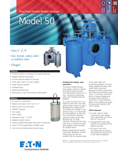
T rouble-free design, easy operationThe Eaton Model 50 plug type duplex strainer's design is simple and economical. This high-quality strainer is, in fact, a pressure rated plug valve with integral straining baskets.To switch the flow from one basket to the other, the oper-ating handle moves through a 90-degree arc. Because of the unique port design in the diverter plug, it is impossible for this operation to stop the flow. The entire switching operation takes fewer than 30 seconds, no toolsrequired. Positioning the plug each time in exactly the right spot happens automatically by integral stops.Before operating the handle, a specially designed, manual lifting jack built into thestrainer, lifts the diverter plugoff its seat. After theswitching operation, the jack easily reseats the plug, even under high pressures.Because a built-in stop limits the distance the diverter plug rises, it minimizes the possi-bility of material bypassing the plug while rotated to divert flow. It also prevents debris from building up under the plug and making it diffi-cult to reseat.Other features• A quick, easy to open, swing-away yoke design cover goes back on just as fast as it came off • Standard NPT drain taps simplify the draining of the basket chamber • All sizes come withmounting legs for bolting the strainer to the floor for a rock solid installationFeatures• Continuous flow, no shutdown for basket cleaning • Rugged tapered plug design • Lift jack prevents galling of the plug • Quick open cover—no tools needed • Large capacity baskets • Threaded drain • Machined basket seat• Perforated or mesh 316 stainless steel basketOptions• Ductile iron construction• Basket perforations from 1/32" to 1/2"• Basket mesh from 20 to 400• MONEL ® baskets • Vent valves • Drain valves• Gauge/vent taps - 1/4" NPT • Magnetic basket inserts• Pressure differential gauge and switch connections • Viton ®, PTFE encapsulated or EPDM seals • Cast iron and stainless steel diverter plug• Sizes 5", 6", 8"• I ron, bronze, carbon steel or stainless steel• FlangedMONEL ® is a registered trademark of Special Metals Corporation group of Companies. Viton ® is a registered trademark of The Chemours Company FC, LLC.C a s t C o n s t r u c t i o nP e r m a n e M e d i aPlug T ype Duplex Basket StrainerSelection chart 5", 6", 8" Iron Bronze Flanged 125# Buna-N ®Flow rate (water) [GPM]P r e s s u r e d r o p [k P a ]5"Bronze 457229********* 8451,04110437132481876"Carbon steel 559327298502470 8891,0671052716318263Stainless steel 559327298502470 8891,0671052716318279Cast iron 559327298502495 9211,0671052716318227Bronze 546273298502384 8701,06710540162862648"Carbon steel 635356–711570 1,2701,4221578122432730Stainless steel 635356–711570 1,2701,4221578122432757Cast iron 635356–711586 1,2861,4221578124432682Bronze635356–7115861,2861,4221578124432782For more information, please email us at ********************or visit /filtration© 2023 Eaton. All rights reserved. All trademarks and registered trademarks are the property of their respective owners. All information and recommenda-tions appearing in this brochure concerning the use of products described herein are based on tests believed to be reliable. However, it is the user’s responsibility to determine the suitability for his own use of such products. Since the actual use by others is beyond our control, no guarantee, expressed or implied, is made by Eaton as to the effects of such use or the results to be obtained. Eaton assumes no liability arising out of the use by others of such products. Nor is the infor-mation herein to be construed as absolutely complete, since additional information may be necessary or desirable when particular or exceptional conditions or circumstances exist or because of applicable laws or government regulations.North America 44 Apple StreetTinton Falls, NJ 07724Toll Free: 800 656-3344 (North America only)Tel: +1 732 212-4700Europe/Africa/Middle East Auf der Heide 253947 Nettersheim, Germany Tel: +49 2486 809-0Friedensstraße 4168804 Altlußheim, Germany Tel: +49 6205 2094-0An den Nahewiesen 2455450 Langenlonsheim, Germany Tel: +49 6704 204-0Greater China No. 7, Lane 280, Linhong RoadChangning District, 200335 Shanghai, P .R. China Tel: +86 21 2899-3687Asia-Pacific100G Pasir Panjang Road #07-08 Interlocal Centre Singapore 118523Tel: +65 6825-1620ENEF -SSEA-1210-2023Partial cutaway of Model 50 duplex strainer clearly illustrates all major parts—and gives a clear indication of the simplicity of design and ease of maintenance.plugJack。
MAX3232EEUE+T中文资料

For pricing, delivery, and ordering information, please contact Maxim Direct at 1-888-629-4642,or visit Maxim's website at .General DescriptionThe MAX3222E/MAX3232E/MAX3237E/MAX3241E/MAX3246E +3.0V-powered EIA/TIA-232 and V.28/V.24communications interface devices feature low power con-sumption, high data-rate capabilities, and enhanced electrostatic-discharge (ESD) protection. The enhanced ESD structure protects all transmitter outputs and receiver inputs to ±15kV using IEC 1000-4-2 Air-G ap Discharge, ±8kV using IEC 1000-4-2 Contact Discharge (±9kV for MAX3246E), and ±15kV using the Human Body Model. The logic and receiver I/O pins of the MAX3237E are protected to the above standards, while the transmit-ter output pins are protected to ±15kV using the Human Body Model.A proprietary low-dropout transmitter output stage delivers true RS-232 performance from a +3.0V to +5.5V power supply, using an internal dual charge pump. The charge pump requires only four small 0.1µF capacitors for opera-tion from a +3.3V supply. Each device guarantees opera-tion at data rates of 250kbps while maintaining RS-232output levels. The MAX3237E guarantees operation at 250kbps in the normal operating mode and 1Mbps in the MegaBaud™ operating mode, while maintaining RS-232-compliant output levels.The MAX3222E/MAX3232E have two receivers and two transmitters. The MAX3222E features a 1µA shutdown mode that reduces power consumption in battery-pow-ered portable systems. The MAX3222E receivers remain active in shutdown mode, allowing monitoring of external devices while consuming only 1µA of supply current. The MAX3222E and MAX3232E are pin, package, and func-tionally compatible with the industry-standard MAX242and MAX232, respectively.The MAX3241E/MAX3246E are complete serial ports (three drivers/five receivers) designed for notebook and subnotebook computers. The MAX3237E (five drivers/three receivers) is ideal for peripheral applications that require fast data transfer. These devices feature a shut-down mode in which all receivers remain active, while consuming only 1µA (MAX3241E/MAX3246E) or 10nA (MAX3237E).The MAX3222E, MAX3232E, and MAX3241E are avail-able in space-saving SO, SSOP, TQFN and TSSOP pack-ages. The MAX3237E is offered in an SSOP package.The MAX3246E is offered in the ultra-small 6 x 6 UCSP™package.ApplicationsBattery-Powered Equipment PrintersCell PhonesSmart Phones Cell-Phone Data Cables xDSL ModemsNotebook, Subnotebook,and Palmtop ComputersNext-Generation Device Features♦For Space-Constrained ApplicationsMAX3228E/MAX3229E: ±15kV ESD-Protected, +2.5V to +5.5V, RS-232 Transceivers in UCSP ♦For Low-Voltage or Data Cable ApplicationsMAX3380E/MAX3381E: +2.35V to +5.5V, 1µA, 2Tx/2Rx, RS-232 Transceivers with ±15kV ESD-Protected I/O and Logic PinsMAX3222E/MAX3232E/MAX3237E/MAX3241E †/MAX3246E±15kV ESD-Protected, Down to 10nA, 3.0V to 5.5V ,Up to 1Mbps, True RS-232 Transceivers________________________________________________________________Maxim Integrated Products 119-1298; Rev 11; 10/07Ordering Information continued at end of data sheet.*Dice are tested at T A = +25°C, DC parameters only.**EP = Exposed paddle.Pin Configurations, Selector Guide, and Typical Operating Circuits appear at end of data sheet.MegaBaud and UCSP are trademarks of Maxim Integrated Products, Inc.†Covered by U.S. Patent numbers 4,636,930; 4,679,134;4,777,577; 4,797,899; 4,809,152; 4,897,774; 4,999,761; and other patents pending.M A X 3222E /M A X 3232E /M A X 3237E /M A X 3241E †/M A X 3246EUp to 1Mbps, True RS-232 TransceiversABSOLUTE MAXIMUM RATINGSELECTRICAL CHARACTERISTICS(V CC = +3V to +5.5V, C1–C4 = 0.1µF, T A = T MIN to T MAX , unless otherwise noted. Typical values are at T A = +25°C.) (Notes 3, 4)Stresses beyond those listed under “Absolute Maximum Ratings” may cause permanent damage to the device. These are stress ratings only, and functional operation of the device at these or any other conditions beyond those indicated in the operational sections of the specifications is not implied. Exposure to absolute maximum rating conditions for extended periods may affect device reliability.V CC to GND..............................................................-0.3V to +6V V+ to GND (Note 1)..................................................-0.3V to +7V V- to GND (Note 1)...................................................+0.3V to -7V V+ + |V-| (Note 1).................................................................+13V Input Voltages T_IN, EN , SHDN , MBAUD to GND ........................-0.3V to +6V R_IN to GND.....................................................................±25V Output Voltages T_OUT to GND...............................................................±13.2V R_OUT, R_OUTB (MAX3241E)................-0.3V to (V CC + 0.3V)Short-Circuit Duration, T_OUT to GND.......................Continuous Continuous Power Dissipation (T A = +70°C)16-Pin SSOP (derate 7.14mW/°C above +70°C)..........571mW 16-Pin TSSOP (derate 9.4mW/°C above +70°C).......754.7mW 16-Pin TQFN (derate 20.8mW/°C above +70°C).....1666.7mW 16-Pin Wide SO (derate 9.52mW/°C above +70°C).....762mW 18-Pin Wide SO (derate 9.52mW/°C above +70°C).....762mW 18-Pin PDIP (derate 11.11mW/°C above +70°C)..........889mW 20-Pin TQFN (derate 21.3mW/°C above +70°C)........1702mW 20-Pin TSSOP (derate 10.9mW/°C above +70°C)........879mW 20-Pin SSOP (derate 8.00mW/°C above +70°C)..........640mW 28-Pin SSOP (derate 9.52mW/°C above +70°C)..........762mW 28-Pin Wide SO (derate 12.50mW/°C above +70°C).............1W 28-Pin TSSOP (derate 12.8mW/°C above +70°C)......1026mW 32-Lead Thin QFN (derate 33.3mW/°C above +70°C)..2666mW 6 x 6 UCSP (derate 12.6mW/°C above +70°C).............1010mW Operating Temperature Ranges MAX32_ _EC_ _...................................................0°C to +70°C MAX32_ _EE_ _.................................................-40°C to +85°C Storage Temperature Range.............................-65°C to +150°C Lead Temperature (soldering, 10s).................................+300°C Bump Reflow Temperature (Note 2)Infrared, 15s..................................................................+200°C Vapor Phase, 20s..........................................................+215°C Note 1:V+ and V- can have maximum magnitudes of 7V, but their absolute difference cannot exceed 13V.Note 2:This device is constructed using a unique set of packaging techniques that impose a limit on the thermal profile the devicecan be exposed to during board-level solder attach and rework. This limit permits only the use of the solder profiles recom-mended in the industry-standard specification, JEDEC 020A, paragraph 7.6, Table 3 for IR/VPR and convection reflow.Preheating is required. Hand or wave soldering is not allowed.MAX3222E/MAX3232E/MAX3237E/MAX3241E †/MAX3246EUp to 1Mbps, True RS-232 Transceivers_______________________________________________________________________________________3M A X 3222E /M A X 3232E /M A X 3237E /M A X 3241E †/M A X 3246EUp to 1Mbps, True RS-232 Transceivers4_______________________________________________________________________________________TIMING CHARACTERISTICS—MAX3237E(V CC = +3V to +5.5V, C1–C4 = 0.1µF, T A = T MIN to T MAX , unless otherwise noted. Typical values are at T A = +25°C.) (Note 3)±10%. MAX3237E: C1–C4 = 0.1µF tested at +3.3V ±5%, C1–C4 = 0.22µF tested at +3.3V ±10%; C1 = 0.047µF, C2, C3, C4 =0.33µF tested at +5.0V ±10%. MAX3246E; C1-C4 = 0.22µF tested at +3.3V ±10%; C1 = 0.22µF, C2, C3, C4 = 0.54µF tested at 5.0V ±10%.Note 4:MAX3246E devices are production tested at +25°C. All limits are guaranteed by design over the operating temperature range.Note 5:The MAX3237E logic inputs have an active positive feedback resistor. The input current goes to zero when the inputs are atthe supply rails.Note 6:MAX3241EEUI is specified at T A = +25°C.Note 7:Transmitter skew is measured at the transmitter zero crosspoints.TIMING CHARACTERISTICS—MAX3222E/MAX3232E/MAX3241E/MAX3246EMAX3222E/MAX3232E/MAX3237E/MAX3241E †/MAX3246EUp to 1Mbps, True RS-232 Transceivers_______________________________________________________________________________________5-6-4-202460MAX3237ETRANSMITTER OUTPUT VOLTAGE vs. LOAD CAPACITANCE (MBAUD = GND)LOAD CAPACITANCE (pF)T R A N S M I T T E R O U T P U T V O L T A G E (V )10001500500200025003000531-1-3-5-6-2-42046-5-31-135010001500500200025003000LOAD CAPACITANCE (pF)T R A N S M I T T E R O U T P U T V O L T A G E (V )MAX3237ETRANSMITTER OUTPUT VOLTAGEvs. LOAD CAPACITANCE-7.5-5.0-2.502.55.07.5MAX3237ETRANSMITTER OUTPUT VOLTAGE vs. LOAD CAPACITANCE (MBAUD = V CC )LOAD CAPACITANCE (pF)T R A N S M I T T E R O U T P U T V O L T A G E (V )500100015002000__________________________________________Typical Operating Characteristics(V CC = +3.3V, 250kbps data rate, 0.1µF capacitors, all transmitters loaded with 3k Ωand C L , T A = +25°C, unless otherwise noted.)-6-5-4-3-2-10123456010002000300040005000MAX3241ETRANSMITTER OUTPUT VOLTAGEvs. LOAD CAPACITANCELOAD CAPACITANCE (pF)T R A N S M I T T E R O U T P U T V O L T A G E (V)302010405060020001000300040005000MAX3241EOPERATING SUPPLY CURRENT vs. LOAD CAPACITANCELOAD CAPACITANCE (pF)S U P P L Y C U R R E N T (m A )04286121014010002000300040005000MAX3241ESLEW RATE vs. LOAD CAPACITANCEM A X 3237E t o c 05LOAD CAPACITANCE (pF)S L E W R A T E (V /μs )-6-5-4-3-2-10123456010002000300040005000MAX3222E/MAX3232ETRANSMITTER OUTPUT VOLTAGEvs. LOAD CAPACITANCELOAD CAPACITANCE (pF)T R A N S M I T T E R O U T P UT V O L T A G E (V )624108141216010002000300040005000MAX3222E/MAX3232ESLEW RATE vs. LOAD CAPACITANCELOAD CAPACITANCE (pF)S L E W R A T E (V /μs)2520155103530404520001000300040005000MAX3222E/MAX3232E OPERATING SUPPLY CURRENT vs. LOAD CAPACITANCELOAD CAPACITANCE (pF)S U P P L Y C U R R E N T (m A )M A X 3222E /M A X 3232E /M A X 3237E /M A X 3241E †/M A X 3246EUp to 1Mbps, True RS-232 Transceivers6_______________________________________________________________________________________Typical Operating Characteristics (continued)(V CC = +3.3V, 250kbps data rate, 0.1µF capacitors, all transmitters loaded with 3k Ωand C L , T A = +25°C, unless otherwise noted.)20604080100MAX3237ETRANSMITTER SKEW vs. LOAD CAPACITANCE(MBAUD = V CC )LOAD CAPACITANCE (pF)100015005002000T R A N S M I T T E R S K E W (n s )-6-2-42046-3-51-1352.03.03.52.54.04.55.0SUPPLY VOLTAGE (V)T R A N S M I T T E R O U T P U T V O L T A G E (V )MAX3237ETRANSMITTER OUTPUT VOLTAGE vs. SUPPLY VOLTAGE (MBAUD = GND)10203040502.0MAX3237E SUPPLY CURRENT vs. SUPPLY VOLTAGE (MBAUD = GND)SUPPLY VOLTAGE (V)S U P P L Y C U R R E N T (m A )3.03.52.54.04.55.0MAX3246ETRANSMITTER OUTPUT VOLTAGEvs. LOAD CAPACITANCELOAD CAPACITANCE (pF)T R A N S M I T T E R O U T P U T V O L T A G E (V )4000300010002000-5-4-3-2-101234567-65000468101214160MAX3246ESLEW RATE vs. LOAD CAPACITANCELOAD CAPACITANCE (pF)S L EW R A T E (V /μs )200030001000400050001020304050600MAX3246EOPERATING SUPPLY CURRENT vs. LOAD CAPACITANCEM A X 3237E t o c 17LOAD CAPACITANCE (pF)S U P P L Y C U R R EN T (m A )1000200030004000500055453525155024681012MAX3237ESLEW RATE vs. LOAD CAPACITANCE(MBAUD = GND)LOAD CAPACITANCE (pF)S L E W R A T E (V /μs )10001500500200025003000010203050406070MAX3237ESLEW RATE vs. LOAD CAPACITANCE(MBAUD = V CC )LOAD CAPACITANCE (pF)S L E W R A T E (V /μs )5001000150020001020304050MAX3237ESUPPLY CURRENT vs. LOAD CAPACITANCE WHEN TRANSMITTING DATA (MBAUD = GND)LOAD CAPACITANCE (pF)S U P P L Y C U R R E N T (m A )10001500500200025003000MAX3222E/MAX3232E/MAX3237E/MAX3241E †/MAX3246EUp to 1Mbps, True RS-232 Transceivers_______________________________________________________________________________________7Pin DescriptionM A X 3222E /M A X 3232E /M A X 3237E /M A X 3241E †/M A X 3246EUp to 1Mbps, True RS-232 Transceivers8_______________________________________________________________________________________MAX3222E/MAX3232E/MAX3237E/MAX3241E †/MAX3246EUp to 1Mbps, True RS-232 Transceivers_______________________________________________________________________________________9Detailed DescriptionDual Charge-Pump Voltage ConverterThe MAX3222E/MAX3232E/MAX3237E/MAX3241E/MAX3246Es’ internal power supply consists of a regu-lated dual charge pump that provides output voltages of +5.5V (doubling charge pump) and -5.5V (inverting charge pump) over the +3.0V to +5.5V V CC range. The charge pump operates in discontinuous mode; if the output voltages are less than 5.5V, the charge pump is enabled, and if the output voltages exceed 5.5V, the charge pump is disabled. Each charge pump requires a flying capacitor (C1, C2) and a reservoir capacitor (C3, C4) to generate the V+ and V- supplies (Figure 1).RS-232 TransmittersThe transmitters are inverting level translators that con-vert TTL/CMOS-logic levels to ±5V EIA/TIA-232-compli-ant levels.The MAX3222E/MAX3232E/MAX3237E/MAX3241E/MAX3246E transmitters guarantee a 250kbps data rate with worst-case loads of 3k Ωin parallel with 1000pF,providing compatibility with PC-to-PC communication software (such as LapLink™). Transmitters can be par-alleled to drive multiple receivers or mice.The MAX3222E/MAX3237E/MAX3241E/MAX3246E transmitters are disabled and the outputs are forcedinto a high-impedance state when the device is in shut-down mode (SHDN = G ND). The MAX3222E/MAX3232E/MAX3237E/MAX3241E/MAX3246E permit the outputs to be driven up to ±12V in shutdown.The MAX3222E/MAX3232E/MAX3241E/MAX3246E transmitter inputs do not have pullup resistors. Connect unused inputs to GND or V CC . The MAX3237E’s trans-mitter inputs have a 400k Ωactive positive-feedback resistor, allowing unused inputs to be left unconnected.MAX3237E MegaBaud OperationFor higher-speed serial communications, the MAX3237E features MegaBaud operation. In MegaBaud operating mode (MBAUD = V CC ), the MAX3237E transmitters guarantee a 1Mbps data rate with worst-case loads of 3k Ωin parallel with 250pF for +3.0V < V CC < +4.5V. For +5V ±10% operation, the MAX3237E transmitters guarantee a 1Mbps data rate into worst-case loads of 3k Ωin parallel with 1000pF.RS-232 ReceiversThe receivers convert RS-232 signals to CMOS-logic output levels. The MAX3222E/MAX3237E/MAX3241E/MAX3246E receivers have inverting three-state outputs.Drive EN high to place the receiver(s) into a high-impedance state. Receivers can be either active or inactive in shutdown (Table 1).Figure 1. Slew-Rate Test CircuitsLapLink is a trademark of Traveling Software.M A X 3222E /M A X 3232E /M A X 3237E /M A X 3241E †/M A X 3246EUp to 1Mbps, True RS-232 Transceivers10______________________________________________________________________________________The complementary outputs on the MAX3237E/MAX3241E (R_OUTB) are always active, regardless of the state of EN or SHDN . This allows the device to be used for ring indicator applications without forward biasing other devices connected to the receiver outputs. This is ideal for systems where V CC drops to zero in shutdown to accommodate peripherals such as UARTs (Figure 2).MAX3222E/MAX3237E/MAX3241E/MAX3246E Shutdown ModeSupply current falls to less than 1µA in shutdown mode (SHDN = low). The MAX3237E’s supply current falls to10nA (typ) when all receiver inputs are in the invalid range (-0.3V < R_IN < +0.3). When shut down, the device’s charge pumps are shut off, V+ is pulled down to V CC , V- is pulled to ground, and the transmitter out-puts are disabled (high impedance). The time required to recover from shutdown is typically 100µs, as shown in Figure 3. Connect SHDN to V CC if shutdown mode is not used. SHDN has no effect on R_OUT or R_OUTB (MAX3237E/MAX3241E).±15kV ESD ProtectionAs with all Maxim devices, ESD-protection structures are incorporated to protect against electrostatic dis-charges encountered during handling and assembly.The driver outputs and receiver inputs of the MAX3222E/MAX3232E/MAX3237E/MAX3241E/MAX3246E have extra protection against static electricity. Maxim’s engineers have developed state-of-the-art structures to protect these pins against ESD of ±15kV without damage.The ESD structures withstand high ESD in all states:normal operation, shutdown, and powered down. After an ESD event, Maxim’s E versions keep working without latchup, whereas competing RS-232 products can latch and must be powered down to remove latchup.Furthermore, the MAX3237E logic I/O pins also have ±15kV ESD protection. Protecting the logic I/O pins to ±15kV makes the MAX3237E ideal for data cable applications.SHDN T2OUTT1OUT5V/div2V/divV CC = 3.3V C1–C4 = 0.1μFFigure 3. Transmitter Outputs Recovering from Shutdown or Powering UpMAX3222E/MAX3232E/MAX3237E/MAX3241E †/MAX3246EUp to 1Mbps, True RS-232 TransceiversESD protection can be tested in various ways; the transmitter outputs and receiver inputs for the MAX3222E/MAX3232E/MAX3241E/MAX3246E are characterized for protection to the following limits:•±15kV using the Human Body Model•±8kV using the Contact Discharge method specified in IEC 1000-4-2•±9kV (MAX3246E only) using the Contact Discharge method specified in IEC 1000-4-2•±15kV using the Air-G ap Discharge method speci-fied in IEC 1000-4-2Figure 4a. Human Body ESD Test ModelFigure 4b. Human Body Model Current WaveformFigure 5a. IEC 1000-4-2 ESD Test Model Figure 5b. IEC 1000-4-2 ESD Generator Current WaveformM A X 3222E /M A X 3232E /M A X 3237E /M A X 3241E †/M A X 3246EUp to 1Mbps, True RS-232 Transceiverscharacterized for protection to ±15kV per the Human Body Model.ESD Test ConditionsESD performance depends on a variety of conditions.Contact Maxim for a reliability report that documents test setup, test methodology, and test results.Human Body ModelFigure 4a shows the Human Body Model, and Figure 4b shows the current waveform it generates when dis-charged into a low impedance. This model consists of a 100pF capacitor charged to the ESD voltage of interest,which is then discharged into the test device through a 1.5k Ωresistor.IEC 1000-4-2The IEC 1000-4-2 standard covers ESD testing and performance of finished equipment; it does not specifi-cally refer to integrated circuits. The MAX3222E/MAX3232E/MAX3237E/MAX3241E/MAX3246E help you design equipment that meets level 4 (the highest level)of IEC 1000-4-2, without the need for additional ESD-protection components.The major difference between tests done using the Human Body Model and IEC 1000-4-2 is higher peak current in IEC 1000-4-2, because series resistance is lower in the IEC 1000-4-2 model. Hence, the ESD with-stand voltage measured to IEC 1000-4-2 is generally lower than that measured using the Human Body Model. Figure 5a shows the IEC 1000-4-2 model, and Figure 5b shows the current waveform for the ±8kV IEC 1000-4-2 level 4 ESD Contact Discharge test. The Air-G ap Discharge test involves approaching the device with a charged probe. The Contact Discharge method connects the probe to the device before the probe is energized.Machine ModelThe Machine Model for ESD tests all pins using a 200pF storage capacitor and zero discharge resis-tance. Its objective is to emulate the stress caused by contact that occurs with handling and assembly during manufacturing. All pins require this protection during manufacturing, not just RS-232 inputs and outputs.Therefore, after PC board assembly, the Machine Model is less relevant to I/O ports.Table 2. Required Minimum Capacitor ValuesFigure 6a. MAX3241E Transmitter Output Voltage vs. Load Current Per TransmitterTable 3. Logic-Family Compatibility with Various Supply VoltagesMAX3222E/MAX3232E/MAX3237E/MAX3241E †/MAX3246EUp to 1Mbps, True RS-232 TransceiversApplications InformationCapacitor SelectionThe capacitor type used for C1–C4 is not critical for proper operation; polarized or nonpolarized capacitors can be used. The charge pump requires 0.1µF capaci-tors for 3.3V operation. For other supply voltages, see Table 2 for required capacitor values. Do not use val-ues smaller than those listed in Table 2. Increasing the capacitor values (e.g., by a factor of 2) reduces ripple on the transmitter outputs and slightly reduces power consumption. C2, C3, and C4 can be increased without changing C1’s value. However, do not increase C1without also increasing the values of C2, C3, C4,and C BYPASS to maintain the proper ratios (C1 to the other capacitors).When using the minimum required capacitor values,make sure the capacitor value does not degradeexcessively with temperature. If in doubt, use capaci-tors with a larger nominal value. The capacitor’s equiv-alent series resistance (ESR), which usually rises at low temperatures, influences the amount of ripple on V+and V-.Power-Supply DecouplingIn most circumstances, a 0.1µF V CC bypass capacitor is adequate. In applications sensitive to power-supply noise, use a capacitor of the same value as charge-pump capacitor C1. Connect bypass capacitors as close to the IC as possible.Operation Down to 2.7VTransmitter outputs meet EIA/TIA-562 levels of ±3.7V with supply voltages as low as 2.7V.Figure 6b. Mouse Driver Test CircuitM A X 3222E /M A X 3232E /M A X 3237E /M A X 3241E †/M A X 3246EUp to 1Mbps, True RS-232 TransceiversFigure 7. Loopback Test CircuitT1IN T1OUTR1OUT5V/div5V/div5V/divV CC = 3.3V C1–C4 = 0.1μFFigure 8. MAX3241E Loopback Test Result at 120kbps T1INT1OUTR1OUT5V/div5V/div5V/divV CC = 3.3V, C1–C4 = 0.1μFFigure 9. MAX3241E Loopback Test Result at 250kbps+5V 0+5V 0-5V +5VT_INT_OUT5k Ω + 250pFR_OUTV CC = 3.3V C1–C4 = 0.1μFFigure 10. MAX3237E Loopback Test Result at 1000kbps (MBAUD = V CC )Transmitter Outputs Recoveringfrom ShutdownFigure 3 shows two transmitter outputs recovering from shutdown mode. As they become active, the two trans-mitter outputs are shown going to opposite RS-232 levels (one transmitter input is high; the other is low). Each transmitter is loaded with 3k Ωin parallel with 2500pF.The transmitter outputs display no ringing or undesir-able transients as they come out of shutdown. Note thatthe transmitters are enabled only when the magnitude of V- exceeds approximately -3.0V.Mouse DrivabilityThe MAX3241E is designed to power serial mice while operating from low-voltage power supplies. It has been tested with leading mouse brands from manu-facturers such as Microsoft and Logitech. The MAX3241E successfully drove all serial mice tested and met their current and voltage requirements.MAX3222E/MAX3232E/MAX3237E/MAX3241E †/MAX3246EUp to 1Mbps, True RS-232 TransceiversFigure 6a shows the transmitter output voltages under increasing load current at +3.0V. Figure 6b shows a typical mouse connection using the MAX3241E.High Data RatesThe MAX3222E/MAX3232E/MAX3237E/MAX3241E/MAX3246E maintain the RS-232 ±5V minimum transmit-ter output voltage even at high data rates. Figure 7shows a transmitter loopback test circuit. Figure 8shows a loopback test result at 120kbps, and Figure 9shows the same test at 250kbps. For Figure 8, all trans-mitters were driven simultaneously at 120kbps into RS-232 loads in parallel with 1000pF. For Figure 9, a single transmitter was driven at 250kbps, and all transmitters were loaded with an RS-232 receiver in parallel with 1000pF.The MAX3237E maintains the RS-232 ±5.0V minimum transmitter output voltage at data rates up to 1Mbps.Figure 10 shows a loopback test result at 1Mbps with MBAUD = V CC . For Figure 10, all transmitters were loaded with an RS-232 receiver in parallel with 250pF.Interconnection with 3V and 5V LogicThe MAX3222E/MAX3232E/MAX3237E/MAX3241E/MAX3246E can directly interface with various 5V logic families, including ACT and HCT CMOS. See Table 3for more information on possible combinations of inter-connections.UCSP ReliabilityThe UCSP represents a unique packaging form factor that may not perform equally to a packaged product through traditional mechanical reliability tests. UCSP reliability is integrally linked to the user’s assembly methods, circuit board material, and usage environ-ment. The user should closely review these areas when considering use of a UCSP package. Performance through Operating Life Test and Moisture Resistance remains uncompromised as the wafer-fabrication process primarily determines it.Mechanical stress performance is a greater considera-tion for a UCSP package. UCSPs are attached through direct solder contact to the user’s PC board, foregoing the inherent stress relief of a packaged product lead frame. Solder joint contact integrity must be consid-ered. Table 4 shows the testing done to characterize the UCSP reliability performance. In conclusion, the UCSP is capable of performing reliably through envi-ronmental stresses as indicated by the results in the table. Additional usage data and recommendations are detailed in the UCSP application note, which can be found on Maxim’s website at .Table 4. Reliability Test DataM A X 3222E /M A X 3232E /M A X 3237E /M A X 3241E †/M A X 3246EUp to 1Mbps, True RS-232 Transceivers__________________________________________________________Pin ConfigurationsMAX3222E/MAX3232E/MAX3237E/MAX3241E †/MAX3246EUp to 1Mbps, True RS-232 TransceiversPin Configurations (continued)M A X 3222E /M A X 3232E /M A X 3237E /M A X 3241E †/M A X 3246EUp to 1Mbps, True RS-232 Transceivers__________________________________________________Typical Operating CircuitsMAX3222E/MAX3232E/MAX3237E/MAX3241E †/MAX3246EUp to 1Mbps, True RS-232 Transceivers_____________________________________Typical Operating Circuits (continued)M A X 3222E /M A X 3232E /M A X 3237E /M A X 3241E †/M A X 3246EUp to 1Mbps, True RS-232 Transceivers_____________________________________Typical Operating Circuits (continued)MAX3222E/MAX3232E/MAX3237E/MAX3241E †/MAX3246EUp to 1Mbps, True RS-232 Transceivers______________________________________________________________________________________21Selector Guide___________________Chip InformationTRANSISTOR COUNT:MAX3222E/MAX3232E: 1129MAX3237E: 2110MAX3241E: 1335MAX3246E: 842PROCESS: BICMOSOrdering Information (continued)†Requires solder temperature profile described in the AbsoluteMaximum Ratings section. UCSP Reliability is integrally linked to the user’s assembly methods, circuit board material, and environment. Refer to the UCSP Reliability Notice in the UCSP Reliability section of this datasheet for more information.**EP = Exposed paddle.。
LM5026.PDF
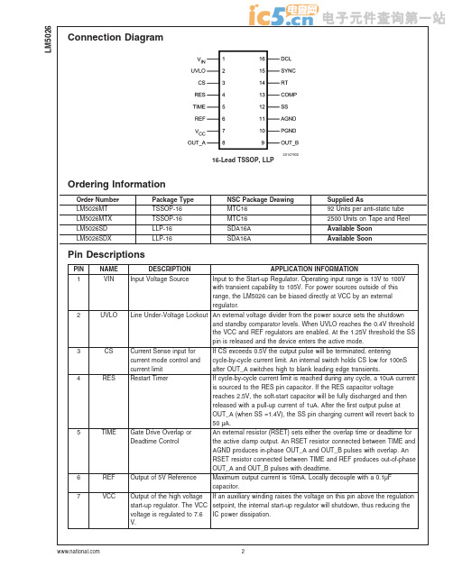
regulator.
2
UVLO Line Under-Voltage Lockout An external voltage divider from the power source sets the shutdown
and standby comparator levels. When UVLO reaches the 0.4V threshold the VCC and REF regulators are enabled. At the 1.25V threshold the SS
Overlap Time = 2.8 x RSET + 2 Deadtime = 2.9 x RSET + 14 With RSET in K Ohms and overlap / deadtime in nanoseconds
Gate Driver Outputs
The LM5026 provides two gate driver outputs, the main power switch control (OUT_A) and the active clamp switch control (OUT_B). The main gate driver features a compound configuration, consisting of both MOS and bipolar devices, which provide superior gate drive characteristics. The bipolar device provides most of the drive current capability and sinks a relatively constant current, which is ideal for driving large power MOSFETs. As the switching event nears conclusion and the bipolar device saturates, the internal MOS device provides a low impedance to compete the switching event.
漏电保护器带空气断路器技术参数
漏电保护器带空气断路器技术参数
漏电保护器带空气断路器是一种常用的电气保护装置,用于保护电路和电气设备免受漏电流和短路电流的损害。
以下是该装置的技术参数:
1. 额定电压:220V/380V
2. 额定频率:50Hz/60Hz
3. 额定漏电动作电流:30mA/100mA
4. 熔断器额定电流:6A/10A/16A/20A/25A/32A/40A/50A/63A
5. 空气断路器额定电流:
6A/10A/16A/20A/25A/32A/40A/50A/63A
6. 额定断路能力:6kA/10kA/16kA
7. 过载保护:空气断路器
8. 短路保护:熔断器
9. 温度保护:热继电器
10. 工作环境温度:-5℃~+40℃
11. 相对湿度:≤50%(40℃时)
12. 安装方式:导轨式/底座式
13. 外壳材质:阻燃塑料
14. 防护等级:IP20
以上是漏电保护器带空气断路器的技术参数,用户在选购时应根据实际需要选择合适的型号及参数。
- 1 -。
en50262标准

en50262标准EN50262标准是欧洲电信领域关于电磁兼容性(EMC)的最新标准,旨在为电信网络中的电磁兼容性提供统一的评估方法。
该标准适用于各种电信设备和系统,包括蜂窝网络、卫星通信、光纤网络等。
本篇文章将详细介绍EN50262标准的背景、内容、测试方法以及实施建议。
一、标准背景随着电信技术的不断发展,电磁兼容性问题日益突出。
为了解决这一问题,欧洲电信领域推出了一系列EMC标准,其中包括EN50262标准。
该标准旨在提供一个统一的评估方法,以便电信设备制造商和运营商能够更好地理解和控制电磁干扰(EMI)。
EN50262标准的实施,有助于提高电信网络的稳定性和可靠性,保障用户通信的质量。
二、标准内容EN50262标准包括以下主要内容:1. 测试标准:规定了电磁兼容测试的各项指标和要求,包括电场强度、磁场强度、谐波失真等。
2. 安全规定:对电信设备中可能产生电磁干扰的因素进行限制,以确保设备在正常使用过程中的安全性。
3. 发射标准:规定了电信设备的辐射发射要求,以确保设备在正常工作状态下不会对其他设备造成干扰。
4. 测试方法和程序:明确了如何进行电磁兼容测试,以及如何评估测试结果。
三、测试方法EN50262标准的测试方法包括以下几个方面:1. 测量场地和设备:测试场地应符合相关标准要求,测量设备应进行校准和验证。
2. 电磁干扰测试:包括电场强度、磁场强度、谐波失真等指标的测量,以确定设备是否产生电磁干扰。
3. 发射测试:对电信设备的辐射发射进行测量,以确定设备是否符合相关标准要求。
4. 接收机灵敏度测试:测试电信设备的接收机灵敏度,以确保其在不同环境下能够正常接收信号。
四、实施建议为了更好地实施EN50262标准,以下建议可供参考:1. 加强培训:组织相关人员参加EMC测试培训,提高测试技能和水平。
2. 规范生产过程:确保生产过程中的每个环节都符合EN50262标准的要求,从源头上控制电磁兼容性问题。
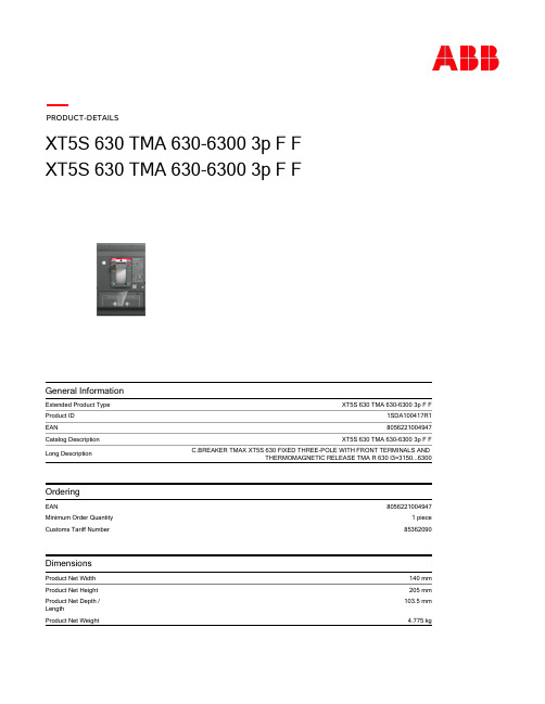
C.BREAKER TMAX XT5S 630 固定三极带前端终端和热磁阀释放TMA R 630 I
Circuit Breaker Type to be Associated Current Type Electrical Durability
Mechanical Durability
Number of Poles Order Multiple Power Loss Product Main Type Product Name Product Type Rated Current (In) Rated Impulse Withstand Voltage (Uimp) Rated Instantaneous Short-Circuit Current Setting (Ii) Rated Insulation Voltage (Ui) Rated Operational Voltage
XT5S 630 TMA 630-6300 3p F F C.BREAKER TMAX XT5S 630 FIXED THREE-POLE WITH FRONT TERMINALS AND
THERMOMAGNETIC RELEASE TMA R 630 I3=3150...6300
8056221004947 1 piece
1SDC210100D0205 1SDC210099D0205 9AKK107680A2824
1SDH002011A1001
Claห้องสมุดไป่ตู้sifications
ETIM 7 Object Classification Code WEEE Category
EC000228 - Power circuit-breaker for trafo/generator/installation protection Q
D5026中文规格书
※ DBIC ※
第 14 页 共 14 页
上海得倍电子技术有限公司
Double Microelectronics Corporation of Shanghai
※ DBIC ※
图 3 时序波形
第 6 页 共 14 页
பைடு நூலகம்
上海得倍电子技术有限公司
Double Microelectronics Corporation of Shanghai
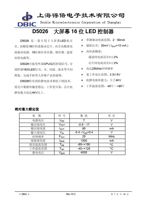
输入及输出等效电路
SSOP-24 4 5 6 7 8 9 10 11 12 13 14 15 16 17 18 19 20 21 22 23 24 1 2 3
管脚名称
LAT OUT0 OUT1 OUT2 OUT3 OUT4 OUT5 OUT6 OUT7 OUT8 OUT9 OUT10 OUT11 OUT12 OUT13 OUT14 OUT15 BLANK SOUT IREF VDD GND SIN SCLK
测试条件 VOH = 17V IOL = 1mA IOH= -1mA
最小值 典型值 最大值 单位
1
uA
0.3 V
3
V
VO ≥0.4V, RSET = 490Ω
36
mA
输出电流
VO ≥0.32V, RSET = 245Ω
72
mA
DIOL1 DIOL2
输出电流(位对位)
VO =1V, RSET = 490Ω. VO = 0.7V, RSET = 245Ω
Double Microelectronics Corporation of Shanghai
应用说明
D5026 高精度恒流特性和低压降特性
由于D5026 采用了高精度恒流驱动电路和温度补偿电路,确保芯片在不同的温度条件、不同的工作 电压和恶劣的使用环境下,位输出电流IOUT恒流效果好。
长运通CYT5026规格书
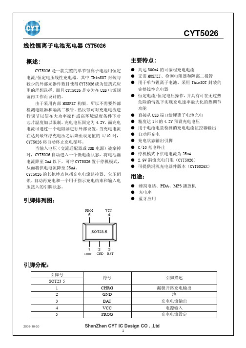
线性锂离子电池充电器CYT5026引脚排列图:引脚分配:引脚号 SOT23-5符号引脚描述1 CHRG 漏极开路充电输出2 GND 地3 BAT 充电电流输出4 VCC 电源输入5 PROG充电电流设定概述:CYT5026是一款完整的单节锂离子电池用恒定电流/恒定电压线性充电器。
其中ThinSOT 封装与较少的外部元器件数目使得CYT5026成为便携式应用的理想选择。
而且CYT5026是专为在USB 电源规范内工作而设计的。
由于采用内部MOSFET 构架,所以不需要外部检测电阻器和隔离二极管。
热反馈可对充电电流进行调节以便在大功率操作或高环境温度条件下对芯片温度加以限制。
充电电压固定为4.2V,而充电电流可通过一个电阻器进行外部设置。
当充电电流在达到最终浮充电压之后降至设定值的1/10时,CYT5026将自动终止充电循环。
当输入电压(交流适配器或USB 电源)被拿掉时,CYT5026自动进入一个低电流状态,将电池漏电流降至2uA 以下,可将CYT5026置于停机模式,从而将供电电流降至25uA。
CYT5026的其他特点包括充电电流监控器、欠压闭锁、自动再充电和一个用于指示充电结束和输入电压接入的引脚状态。
主要特点:● 高达800mA 的可编程充电电流● 无需MOSFET、检测电阻器和隔离二极管 ● 用于单节锂离子电池、采用ThinSOT 封装的完整线性充电器● 恒定电流/恒定电压操作,并具有可在无过热危险的情况下实现充电速率最大化的热调节功能● 直接从USB 端口给锂离子电池充电 ● 精度达1%的4.2V 预设充电电压● 用于电池电量检测的充电电流监控器输出 ● 自动再充电● 充电状态输出引脚 ● C/10充电终止● 停机模式下供电电流为25uA ● 2.9V 涓流充电门限(CYT5026)● 可提供涓流充电器件版本(CYT5026X)用途:● 蜂窝电话、PDA 、MP3播放机 ● 充电座 ● 蓝牙应用功能框图:极限参数参数 额定值输入电源电压 -0.3V~10VPROG -0.3V~Vcc+0.3VBAT -0.3V~7VCHRG -0.3V~10VBAT短路持续时间 连续BAT引脚电流 800mAPROG引脚电流 800uA最大结温 125℃工作环境工作温度 -40℃~85℃贮存温度环境 -65℃~125℃ 引脚温度(焊接时间10秒) 260℃电气特性:凡标注●表示该指标适合整个工作温度范围,否则仅指T A =25℃,Vcc=5V,除非特别注明。
50p06场效应管参数
50p06场效应管参数场效应管(Field Effect Transistor,简称FET)是一种常用的电子器件,具有高输入阻抗、低输出阻抗、低噪声、低功耗等特点,广泛应用于放大、开关、调节等电路中。
50P06是一种常见的场效应管型号,下面将介绍其主要参数。
首先,50P06的“50”代表了其最大漏极-源极电压(VDS)为50V。
这意味着在正常工作条件下,50P06可以承受最大50V的电压。
在设计电路时,需要根据实际需求选择合适的电源电压,以确保场效应管的正常工作。
其次,P06代表了50P06的漏极电流(ID)为6A。
漏极电流是指场效应管从漏极到源极的电流,也是场效应管的主要工作电流。
50P06的漏极电流为6A,这意味着它可以承受最大6A的电流。
在实际应用中,需要根据电路的负载要求和功率需求选择合适的场效应管。
此外,50P06还有其他重要的参数需要了解。
其中,栅极-源极电压(VGS)是指场效应管的栅极电压与源极电压之间的电压差。
50P06的最大VGS为±20V,这意味着在正常工作条件下,栅极电压与源极电压之间的电压差不应超过20V。
另一个重要的参数是漏极-源极电阻(RDS(on))。
漏极-源极电阻是指场效应管在导通状态下,漏极与源极之间的电阻。
50P06的典型RDS(on)为0.1Ω,这意味着在导通状态下,漏极与源极之间的电阻为0.1Ω。
电阻越小,场效应管的导通能力越好。
此外,50P06还有一些其他参数,如输入电容(Ciss)、输出电容(Coss)、反向传输电容(Crss)等。
这些参数主要影响场效应管的高频特性和开关速度。
在设计高频电路或开关电路时,需要根据这些参数选择合适的场效应管。
综上所述,50P06是一种常见的场效应管型号,具有最大漏极-源极电压为50V、漏极电流为6A等主要参数。
在选择和应用50P06场效应管时,需要根据实际需求和电路要求,合理选择电源电压、电流和其他参数,以确保电路的正常工作和性能优良。
fr106二极管参数

fr106二极管参数FR106是一款具有二极管结构的电子元件,属于快恢复二极管类型。
它具有以下一些参数,我们一一来讨论,详细了解这款二极管。
1.最大重复逆向电压(Maximum Repetitive Reverse Voltage):FR106的最大重复逆向电压为600伏特。
这意味着在使用过程中,二极管的逆向电压不能超过这个值,否则可能会损坏器件。
2.平均整流电流(Average Rectified Current):FR106的平均整流电流是1安培。
这是指二极管在整流电路中的工作电流的平均值。
3.最大峰值反向电流(Maximum Peak Reverse Current):FR106的最大峰值反向电流是30毫安。
这是指二极管在正向工作时,逆向电流的最大值。
4.正向电压降(Forward Voltage Drop):FR106的正向电压降是1.1伏特。
这是指二极管在正向工作时所需的电压。
5.反向恢复时间(Reverse Recovery Time):FR106的反向恢复时间是30纳秒。
这是指二极管从正向导通到开始反向恢复的时间。
6.最大工作温度(Maximum Operating Temperature):FR106的最大工作温度为150摄氏度。
超过这个温度范围,二极管可能会受到损坏。
7.封装类型(Package Type):FR106一般封装为DO-41封装。
这种封装能够确保二极管的稳定性和可靠性,并且容易焊接。
FR106是一款低功耗、高效率的二极管。
它常常被应用在各种电路中,例如开关电源、逆变器、整流电路等。
由于其反向恢复时间非常短,它能够快速地反向恢复,适用于高频电路和高速开关应用。
此外,FR106具有低正向电压降和低反向泄漏电流,能够减小功耗并提高电子设备的效率。
但是需要注意的是,尽管FR106具有较高的最大重复逆向电压和平均整流电流,但在实际应用中,我们还是需要根据具体电路要求选择合适的二极管。
- 1、下载文档前请自行甄别文档内容的完整性,平台不提供额外的编辑、内容补充、找答案等附加服务。
- 2、"仅部分预览"的文档,不可在线预览部分如存在完整性等问题,可反馈申请退款(可完整预览的文档不适用该条件!)。
- 3、如文档侵犯您的权益,请联系客服反馈,我们会尽快为您处理(人工客服工作时间:9:00-18:30)。
(VCC = 5V, SHDN = VCC, TA = -40°C to +85°C, unless otherwise noted. Typical values are at TA = +25°C.) (Note 1)
Features
MAX5025–MAX5028
Applications
TV Tuner Power Supply Low-Noise Varactor Diode Biasing Set-Top Box Tuner Power Supply PCI Cable Modem Voice-Over-Cable LCD Power Supply Avalanche Photodiode Biasing
500kHz, 36V Output, SOT23, PWM Step-Up DC-DC Converters MAX5025–MAX5028
ABSOLUTE MAXIMUM RATINGS
VCC to GND ............................................................-0.3V to +12V PGND to GND .......................................................-0.1V to +0.1V FB to GND (MAX5025/MAX5026)...............-0.3V to (VCC + 0.3V) FB to GND (MAX5027/MAX5028)...........................-0.3V to +40V SHDN to GND.............................................-0.3V to (VCC + 0.3V) LX to GND ..............................................................-0.3V to +45V Peak LX Current ................................................................600mA Operating Temperature Range ...........................-40°C to +85°C Continuous Power Dissipation (TA = +70°C) 6-Pin SOT23 (derate 7.1mW/°C above +70°C)..........695.7mW Junction Temperature ......................................................+150°C Storage Temperature Range .............................-65°C to +165°C Lead Temperature (soldering 10s) ..................................+_____________________________________________________________________________________
元器件交易网
500kHz, 36V Output, SOT23, PWM Step-Up DC-DC Converters
元器件交易网
19-2239; Rev 1; 12/01
KIT ATION EVALU E L B AVAILA
500kHz, 36V Output, SOT23, PWM Step-Up DC-DC Converters
General Description
The MAX5025–MAX5028 constant-frequency, pulsewidth modulating (PWM), low-noise boost converters are intended for low-voltage systems that often need a locally generated high voltage. These devices are capable of generating low-noise, high output voltages required for varactor diode biasing in TV tuners, set-top boxes, and PCI cable modems. The MAX5025– MAX5028 operate from as low as 3V and switch at 500kHz. The constant-frequency, current-mode PWM architecture provides for low output noise that is easy to filter. A 40V lateral DMOS device is used as the internal power switch, making the devices ideal for boost converters up to 36V. The MAX5025/MAX5026 adjustable versions require the use of external feedback resistors to set the output voltage. The MAX5027/MAX5028 offer a fixed 30V output. These devices are available in a small, 6pin SOT23 package. o Input Voltage Range: 3V to 11V (MAX5026/MAX5028) 4.5V to 11V (MAX5025/MAX5027) o Wide Output Voltage Range: VCC to 36V o Output Power: 120mW (max) o User-Adjustable Output Voltage with MAX5025/MAX5026 Using External Feedback Resistors o Fixed 30V Output Voltage: MAX5027/MAX5028 o Internal 1.3Ω (typ), 40V Switch o Constant PWM Frequency Provides Easy Filtering in Low-Noise Applications o 500kHz (typ) Switching Frequency o 1µA (max) Shutdown Current o Small, 6-Pin SOT23 Package
Stresses beyond those listed under “Absolute Maximum Ratings” may cause permanent damage to the device. These are stress ratings only, and functional operation of the device at these or any other conditions beyond those indicated in the operational sections of the specifications is not implied. Exposure to absolute maximum rating conditions for extended periods may affect device reliability.
Typical Operating Circuit
Selector Guide appears at end of data sheet.
VCC = 4.5V TO 11V (MAX5027) VCC = 3V TO 11V (MAX5028) L1 D1 VCC LX
VOUT 30V
Pin Configuration
ELECTRICAL CHARACTERISTICS
(VCC = 5V, SHDN = VCC, TA = -40°C to +85°C, unless otherwise noted. Typical values are at TA = +25°C.) (Note 1)
PARAMETER SUPPLY VOLTAGE Input Voltage Range Undervoltage Lockout Supply Current Shutdown Current BOOST CONVERTER Switching Frequency fSW MAX5025/MAX5027 MAX5026/MAX5028, VCC = 3.3V MAX5025/MAX5027, ILOAD = 2mA, VCC = 4.5V to 11V, VOUT = 30V Line Regulation MAX5026/MAX5028, ILOAD = 0.5mA, VCC = 3V to 11V, VOUT = 30V MAX5025/MAX5027, VCC = 5V, ILOAD = 0 to 4mA, VOUT = 30V Load Regulation MAX5026/MAX5028, VCC = 3.3V, ILOAD = 0 to 1mA, VOUT = 30V Thermal Shutdown Thermal Shutdown Hysteresis 1.0 140 2 °C °C 0.25 345 410 500 500 0.25 %/V 1000 670 kHz VCC VUVLO ICC ISHDN MAX5026/MAX5028 MAX5025/MAX5027 Rise/fall, hysteresis = 3mV MAX5025/MAX5026, FB = 1.4V MAX5027/MAX5028, FB = 35V SHDN = GND 3.0 4.5 2.25 2.65 350 0.01 11 11 2.95 1000 1 V V µA µA SYMBOL CONDITIONS MIN TYP MAX UNITS
