INA826_中文资料
INA333中文资料

• BRIDGE AMPLIFIERS • ECG AMPLIFIERS • PRESSURE SENSORS • MEDICAL INSTRUMENTATION • PORTABLE INSTRUMENTATION • WEIGH SCALES • THERMOCOUPLE AMPLIFIERS • RTD SENSOR AMPLIFIERS • DATA ACQUISITION
Human body model (HBM)
ESD rating
Charged device model (CDM)
ห้องสมุดไป่ตู้
Machine model (MM)
INA333 +7
(V–) – 0.3 to (V+) + 0.3 Continuous
–40 to +150 –65 to +150
+150 4000 1000 200
Click Here
V+
7
2 VIN-
RFI Filtered Inputs
A1 RFI Filtered Inputs 1
50kW
RG 8
50kW
150kW
150kW
A3
6 VOUT
3 VIN+
RFI Filtered Inputs RFI Filtered Inputs
A2
4 V-
150kW
150kW
UNIT V V
°C °C °C V V V
(1) Stresses above these ratings may cause permanent damage. Exposure to absolute maximum conditions for extended periods may degrade device reliability. These are stress ratings only, and functional operation of the device at these or any other conditions beyond those specified is not implied.
ina282中文资料
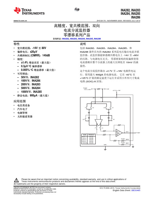
特性
宽共模范围:-14V 至 80V 偏移电压:±20μV 共模抑制比 (CMRR):140dB 精度: – ±1.4% 增益误差(最大值) – 0.3μV/°C 偏移漂移 – 0.005%/°C 增益漂移(最大值) 可用增益: – 50V/V:INA282 – 100V/V:INA286 – 200V/V:INA283 – 500V/V:INA284 – 1000V/V:INA285 静态电流:900μA(最大值)
Supply -14V to +80V Load +2.7V to +18V
• • • •
2
•
•
+IN
-IN
V+
应用范围
• • • • 电信类设备 汽车电子 电源管理 太阳能逆变器
Æ2 1 Æ2 Æ2 Æ1
Æ2
1
Æ1 ZerÆDrift OUT
Output
GAIN 50V/V 100V/V 200V/V 500V/V 1000V/V
版权 © 2009–2010, Texas Instruments Incorporated
UNLESS OTHERWISE NOTED this document contains PRODUCTION DATA information current as of publication date. Products conform to specifications per the terms of Texas Instruments standard warranty. Production processing does not necessarily include testing of all parameters.
AD826AN中文资料

a
High-Speed, Low-Power Dual Operational Amplifier
AD826
FEATURES High Speed:
50 MHz Unity Gain Bandwidth 350 V/s Slew Rate 70 ns Settling Time to 0.01% Low Power: 7.5 mA Max Power Supply Current Per Amp Easy to Use: Drives Unlimited Capacitive Loads 50 mA Min Output Current Per Amplifier Specified for +5 V, ؎5 V and ؎15 V Operation 2.0 V p-p Output Swing into a 150 ⍀ Load
The AD826 excels as an ADC/DAC buffer or active filter in data acquisition systems and achieves a settling time of 70 ns to 0.01%, with a low input offset voltage of 2 mV max. The AD826 is available in small 8-lead plastic mini-DIP and SO packages.
V
± 15 V
50
mA
±5 V
50
mA
0, +5 V
30
mA
± 15 V
90
mA
8
Ω
MATCHING CHARACTERISTICS Dynamic Crosstalk Gain Flatness Match Slew Rate Match DC Input Offset Voltage Match Input Bias Current Match Open-Loop Gain Match
AT824 825 826 手持式 LCR 数字电桥 用户手册说明书

[AT824/825/826 手持式LCR数字电桥]用户手册声明根据国际版权法,未经常州安柏精密仪器有限公司(Applent Instruments Inc.)事先允许和书面同意,不得以任何形式复制本文内容。
安全信息为避免可能的电击和人身安全,请遵循以下指南进行操作。
免责声明用户在开始使用仪器前请仔细阅读以下安全信息,对于用户由于未遵守下列条款而造成的人身安全和财产损失,安柏科技将不承担任何责任。
不可在爆炸性气体环境使用仪器不可在易燃易爆气体、蒸汽或多灰尘的环境下使用仪器。
不可在潮湿环境使用仪器仪器不防水,不要将水滴入仪器测试端,也不要在潮湿环境使用仪器。
不可打开仪器外壳除了电池仓用户可以更换旧电池外,内部没有任何用户需要维护的地方,非专业维护人员不可打开仪器外壳,以试图维修仪器。
不要超出本说明书指定的方式使用仪器超出范围,仪器所提供的保护措施将失效。
警告:不要加直流电压或电流到测试端,否则会损坏仪器。
警告:测试电容器前,确保电容器已放电,否则会损坏仪器。
安全标志:设备由双重绝缘或加强绝缘保护废弃电气和电子设备(WEEE) 指令2002/96/EC切勿丢弃在家庭垃圾中有限担保和责任范围常州安柏精密仪器有限公司(以下简称Applent)保证您购买的每一台仪器在质量和计量上都是完全合格的。
此项保证不包括保险丝以及因疏忽、误用、污染、意外或非正常状况使用造成的损坏。
本项保证仅适用于原购买者,并且不可转让。
自发货之日起,Applent提供玖拾(90)天保换和贰年免费保修,此保证也包括VFD或LCD。
玖拾天保换期内由于使用者操作不当引起的损坏,保换条款终止。
贰年包修期内由于使用者操作不当而引起仪器损坏,维修费用由用户承担。
贰年后直到仪表终生,Applent将以收费方式提供维修。
对于VFD或LCD的更换,其费用以当前成本价格收取。
如发现产品损坏,请和Applent取得联系以取得同意退回或更换的信息。
之后请将此产品送销售商进行退换。
ISO106中文资料
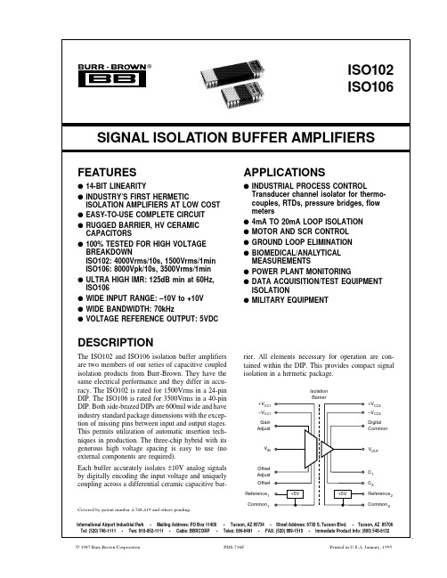
SIGNAL ISOLATION BUFFER AMPLIFIERSAPPLICATIONSq INDUSTRIAL PROCESS CONTROLTransducer channel isolator for thermo-couples, RTDs, pressure bridges, flowISOLATION AMPLIFIERS AT LOW COST2®ISO102/106SPECIFICATIONSELECTRICALAt T A = +25°C and V CC1 = V CC2 = ±15V unless otherwise noted.ISO102, ISO106, ISO102B, ISO106BPARAMETERCONDITIONSMINTYPMAXUNITSISOLATION VoltageRated Continuous (1)ISO102:AC, 60HzT MIN to T MAX 1500Vrms DCT MIN to T MAX 2121VDC ISO106:AC, 60HzT MIN to T MAX 3500Vrms DCT MIN to T MAX4950VDC Test Breakdown, AC, 60Hz ISO10210s 4000Vrms ISO10610s8000Vpk Isolation-Mode Rejection (2)V ISO = Rated Continuous, 60HzAC:ISO102115120dB 12µVrms/V ISO106125130dB 0.30.6µVrms/V DC140160dB 0.010.10µVDC/V Barrier Resistance 1014ΩBarrier Capacitance 6pF Leakage Current V ISO = 240Vrms, 60Hz 0.51µArms INPUTVoltage Range Rated Operation–10+10V Resistance 75100k ΩCapacitance 5pF OUTPUTVoltage RangeRated Operation –10+10V Derated Operation–12+12V Current Drive±5mA Short Circuit Current 92050mA Ripple Voltage (6) f = 0.5MHz to 1.5MHz3mVp-p Resistance0.31ΩCapacitive Load Drive Capability 10,000pF Overload Recovery Time, 0.1%|V O | > 12V30µs OUTPUT VOLTAGE NOISE Voltage:f = 0.1Hz to 10Hz300µVp-p f = 0.1Hz to 70kHz16µV/ Hz Dynamic Range (7):f = 0.1Hz to 70kHz12-Bit Resolution, 1LSB, 20V FS 74dB f = 0.1Hz to 280Hz 16-Bit Resolution, 1LSB, 20V FS96dB FREQUENCY RESPONSE Small Signal Bandwidth70kHz Full Power Bandwidth, 0.1% THD V O = ±10V 5kHz Slew RateV O = ±10V 0.5V/µs Settling Time, 0.1%V O = –10V to +10V100µs Overshoot, Small Signal (8)C 1 = C 2 = 040%VOLTAGE REFERENCES Voltage Output, Ref 1, Ref 2No Load +4.975+5+5.025VDC B GradeNo Load+4.995+5+5.005VDC vs Temperature ±520ppm/°C vs Supplies 10µV/V vs Load4001000µV/mA Current Output–0.1+5mA Short Circuit Current 61430mA POWER SUPPLIESRated Voltage, ±V CC1, ±V CC2Rated Performance±15V Voltage Range±10±20V Quiescent Current:+V CC1No Load+11+15mA –V CC1–9–12mA +V CC2+25+33mA –V CC2–15–20mA Dissipation:±V CC1300400mW ±V CC2600800mW TEMPERATURE RANGE Specification –25+85°C Operating (9)–25+85°C Storage–65+150°C Thermal Resistance, θJA40°C/W θJC12°C/W3®ISO102/106ELECTRICAL (CONT)ISO102ISO102B PARAMETER CONDITIONSMINTYP MAXMINTYP MAXUNITS GAINNominal Gain 1*V/V Initial Error (3)±0.1±0.250.070.13% FSR Gain vs Temperature ±20±50±12±25ppm FSR/°C Nonlinearity (4)V O = –10V to +10V±0.007±0.012±0.002±0.003% FSRINPUT OFFSET VOLTAGE Initial OffsetV IN = 0V±25±70±15±25mV vs Temperature ±250±500±150±250µV/°C vs Power Supplies (5)Input Stage, V CC1 = ±10V to ±20V 0 1.4 4.0***mV/V Output Stage, V CC2 = ±10V to ±20V–4–1.4***mV/VThe information provided herein is believed to be reliable; however, BURR-BROWN assumes no responsibility for inaccuracies or omissions. BURR-BROWN assumes no responsibility for the use of this information, and all use of such information shall be entirely at the user’s own risk. Prices and specifications are subject to change without notice. No patent rights or licenses to any of the circuits described herein are implied or granted to any third party. BURR-BROWN does not authorize or warrant any BURR-BROWN product for use in life support devices and/or systems.ISO106ISO106B PARAMETER CONDITIONSMINTYP MAXMINTYP MAXUNITS GAINNominal Gain 1*V/V Initial Error (3)±0.1±0.250.07*% FSR Gain vs Temperature ±20±50±12±25ppm FSR/°C Nonlinearity (4)V O = –10V to +10V±0.04±0.075±0.007±0.025% FSRINPUT OFFSET VOLTAGE Initial OffsetV IN = 0V±25±70**mV vs Temperature ±250±500±150±250µV/°C vs Power Supplies (5)Input Stage, V CC1 = ±10V to ±20V 3.7*mV/V Output Stage, V CC2 = ±10V to ±20V–3.7*mV/V* Specification same as model to the left.NOTES: (1) 100% tested at rated continuous for one minute. (2) Isolation-mode rejection is the ratio of the change in output voltage to a change in isolation barrier voltage.It is a function of frequency as shown in the Typical Performance Curves. This is specified for barrier voltage slew rates not exceeding 100V/µs. (3) Adjustable to zero.FSR = Full Scale Range = 20V. (4) Nonlinearity is the peak deviation of the output voltage from the best fit straight line. It is expressed as the ratio of deviation to FSR.(5) Power supply rejection = change in V OS /20V supply change. (6) Ripple is the residual component of the barrier carrier frequency generated internally. (7) Dynamic range = FSR/(voltage spectral noise density x square root of user bandwidth). (8) Overshoot can be eliminated by band-limiting. (9) See “Power Dissipation vs Temperature” performance curve for limitations. (10) Band limited to 10Hz, bypass capacitors located less than 0.25" from supply pins.NOTE: (1) For detailed drawing and dimension table, please see end of data sheet, or Appendix D of Burr-Brown IC Data Book.4®ISO102/106PIN CONFIGURATION–V V Gain Adjust Common C Common Reference +V +V Offset Adjust Offset Reference Digital Common C V –V 1 2 3 4 9 10 11 1224 23 22 21 16 15 14 13CC1CC2CC1ISO1021OUT CC22 IsolationBarrierIN112 2–V V Gain Adjust Common C Common Reference +V +V Offset Adjust Offset Reference Digital Common C V –V 1 2 3 4 17 18 19 2040 39 38 37 24 23 22 21CC1CC2 CC1ISO1061OUT CC22 IsolationBarrierIN112 2PIN DESCRIPTIONS±V CC1,Positive and negative power supply voltages and common (or ground) for the input stage. Common 1 is the analog reference voltage for input Common 1signals. The voltage between Common 1 and Common 2 is the isolation voltage and appears across the internal high voltage barrier.±V CC2,Positive and negative power supply voltages and common (or ground) for the output stage. Common 2 is the analog reference voltage for output Common 2signals. The voltage between Common 1 and Common 2 is the isolation voltage and appears across the internal high voltage barrier.V IN Signal input pin. Input impedance is typically 100k Ω. The input range is rated for ±10V. The input level can actually exceed the input stage supplies. Output signal swing is limited only by the output supply voltages.Gain This pin is an optional signal input. A series 5k Ω potentiometer between this pin and the input signal allows a guaranteed ±1.5% gain adjustment Adjust range. When gain adjustment is not required, the Gain Adjust should be left open. Figure 4 illustrates the gain adjustment connection.Reference 1+5V reference output. This low-drift zener voltage reference is necessary for setting the bipolar offset point of the input stage. This pin must be strapped to either Offset or Offset Adjust to allow the isolation amplifier to function. The reference is often useful for input signal conditioning circuits. See “Effect of Reference Loading on Offset” performance curve for the effect of offset voltage change with reference loading.Reference 1 is identical to, but independent of, Reference 2. This output is short circuit protected.Reference 2+5V reference output. This reference circuit is identical to, but independent of, Reference 1. It controls the bipolar offset of the output stage through an internal connection. This output is short-circuit protected.Offset Offset input. This input must be strapped to Reference 1 unless user adjustment of bipolar offset is required.Offset This pin is for optional offset control. When connected to the Reference 1 pin through a 1k Ω potentiometer, ±150mV of adjustment range is Adjust guaranteed. Under this condition, the Offset pin should be connected to the Offset Adjust pin. When offset adjustment is not required, the Offset Adjust pin is left open. See Figure 4.Digital Digital common or ground. This separate ground carries currents from the digital portions of the output stage circuit. The best grounding practi-Common ces require that digital common current does not flow in analog common connections. Both pins can be tied directly to a ground plane if available.Difference in potentials between the Common 2 and Digital Common pins can be ±1V. See Figure 2.V OUTSignal output. Because the isolation amplifier has unity gain, the output signal is ideally identical to the input signal. The output is low impedance and is short-circuit protected. This signal is referenced to Common 2; subsequent circuitry should have a separate “sense” connection to Common 1as well as V OUT .C 1, C 2Capacitors for small signal bandwidth control. These pins connect to the internal rolloff frequency controlling nodes of the output low-pass filter.Additional capacitance added to these pins will modify the bandwidth of the buffer. C 2 is always twice the value of C 1. See “Bandwidth Control”performance curve for the relationship between bandwidth and C 1 and C 2. When no connections are made to these pins, the full small-signal bandwidth is maintained. Be sure to shield C 1 and C 2 pins from high electric fields on the PC board. This preserves AC isolation-mode rejection by reducing capacitive coupling effects.5®ISO102/106TYPICAL PERFORMANCE CURVEST A = +25°C, V CC = ±15VDC unless otherwise noted.ISOLATION-MODE REJECTION vs ISOLATION VOLTAGE FREQUENCYIsolation Voltage Frequency (Hz)I s o l a t i o n -M o d e R e j e c t i o n (d B )1601401201008060 101M1001k10k100kDYNAMIC RANGE vs BANDWIDTHSmall Signal Bandwidth (Hz)Bandwidth Control Capacitors (F)D y n a m i c R a n g e (d B )120110100908070 110 100 1k 10k 100k 3µ300n30n3nF300p30pBW — C — 1ISOLATION LEAKAGE CURRENT vs ISOLATION VOLTAGE FREQUENCYIsolation Voltage Frequency (Hz)I s o l a t i o n L e a k a g e C u r r e n t (A )101M10m1m100µ10µ1µ100n1001k10k100kIsolation Voltage (V)Rated10.5–0.5–1210 –1 –2 GainOffsetT = T to T MIN MAX∆ GAIN ERROR AND ∆ OFFSET VOLTAGEvs ISOLATION VOLTAGEG a i n E r r o r (%)∆ ∆ O f f s e t V o l t a g e (m V )BANDWIDTH CONTROLC 1 (F)S m a l l S i g n a l B a n d w i d t h (H z )1M100k10k 1k 10010 13p30p300p3n 30n300n 3µPOWER DISSIPATION vs TEMPERATUREAmbient Temperature (°C)M a x i m u m P o w e r D i s s i p a t i o n (W )1.61.41.210.80M a x i m u m P o w e r S u p p l i e s (V )±20±15±106®ISO102/106TYPICAL PERFORMANCE CURVES (CONT)T A = +25°C, V CC = ±15VDC unless otherwise noted.LARGE SIGNAL TRANSIENT RESPONSETime (µs)100200 30040015 105 0 –5 –10 –15O u t p u t V o l t a g e (V )TOTAL HARMONIC DISTORTIONFrequency (Hz)1001k 10k100kT H D + N o i s e (%)1010.10 RECOMMENDED RANGE OF ISOLATION VOLTAGEIsolation Voltage Frequency (Hz)1k10k100k1M10k M a x i m u m I s o l a t i o n V o l t a g e (V p k )1k10010 2k 5kGAIN/PHASE vs FREQUENCY101001k10k100kFrequency (Hz)S m a l l S i g n a l G a i n (d B )6–6–12–1890–90–180–270P h a s e S h i f t (d e g r e e s )OUTPUT SPECTRAL NOISE DENSITY40 35 30 25 20 15 10 5 0 S p e c t r a l N o i s e D e n s i t y (d B H z )10µV / H z 01020 30 40 50 Frequency (kHz) N: 128 : 125Hz FS: –47dBVβ GAIN FLATNESS vs FREQUENCY0 1 2 3 4 5 6 7 8Frequency (kHz)L a r g e S i g n a l G a i n (d B )0.030.02 0.01 0 –0.01 –0.02 –0.037®ISO102/106TYPICAL PERFORMANCE CURVES (CONT)T A = +25°C, V CC = ±15VDC unless otherwise noted.FIGURE 1. Simplified Diagram of ISO102 and ISO106.THEORY OF OPERATIONThe ISO102 and ISO106 have no galvanic connection be-tween the input and output. The analog input signal refer-enced to the input common is accurately duplicated at the output referenced to the output common. Because the barrier information is digital, potentials between the two commons can assume a wide range of voltages and frequencies with-out influencing the output signal. Signal information re-mains undisturbed until the slew rate of the barrier voltage exceeds 100V/µs. The isolation amplifier’s ability to reject fast dV/dt changes between the two grounds is specified as transient immunity. The amplifier is protected from damage for slew rates up to 100,000V/µs.A simplified diagram of the ISO102 and ISO106 is shown in Figure 1. The design consists of an input voltage-controlled oscillator (VCO) also known as a voltage-to-frequency con-verter (VFC), differential capacitors, and output phase lock loop (PLL). The input VCO drives digital levels directly into the two 3pF barrier capacitors. The digital signal is fre-quency modulated and appears differentially across the bar-rier, while the externally applied isolation voltage appears common-mode.EFFECT OF REFERENCE LOADING ON OFFSETVoltage Reference Load (mA)1250–50O u t p u t O f f s e t (m V )0.010.005–0.005–0.01ISO102B TYPICAL LINEARITY–100 10V OUT = V IN (V)N o n l i n e a r i t y (%)5–58®ISO102/106A sense amplifier detects only the differential information.The output stage decodes the frequency modulated signal by the means of a PLL. The feedback of the PLL employs a second VCO that is identical to the encoder VCO. The PLL forces the second VCO to operate at the same frequency (and phase) as the encoder VCO; therefore, the two VCOs have the same input voltage. The input voltage of the decoder VCO serves as the isolation buffer’s output signal after passing through a 100kHz second-order active filter.For a more detailed description of the internal operation of the ISO102 and ISO106, refer to Proceedings of the 1987International Symposium on Microelectronics, pages 202-206.ABOUT THE BARRIERFor any isolation product, barrier composition is of para-mount importance in achieving high reliability. Both the ISO102 and ISO106 utilize two 3pF high voltage ceramic coupling capacitors. They are constructed of tungsten thick film deposited in a spiral pattern on a ceramic substrate.Capacitor plates are buried in the package, making the barrier very rugged and hermetically sealed. Capacitance results from the fringing electric fields of adjacent metal runs. Dielectric strength exceeds 10kV and resistance is typically 1014Ω. Input and output circuitry are contained in separate solder-sealed cavities, resulting in the industry’s first fully hermetic hybrid isolation amplifier.FIGURE 3. Technique for Wiring Analog and Digital Com-mons Together.FIGURE 2. Power Supply and Signal Connection.The ISO102 and ISO106 are designed to be free from partial discharge at rated voltages. Partial discharge is a form of localized breakdown that degrades the barrier over time.Since it does not bridge the space across the barrier, it is difficult to detect. Both isolation amplifiers have been exten-sively evaluated at high temperature and high voltage.POWER SUPPLY AND SIGNAL CONNECTIONS Figure 2 shows the proper power supply and signal connec-tions. Each supply should be AC-bypassed to Analog Com-mon with 0.1µF ceramic capacitors as close to the amplifier as possible. Short leads will minimize lead inductance. A ground plane will also reduce noise problems. Signal com-mon lines should tie directly to the common pin even if a low impedance ground plane is used. Refer to Digital Com-mon in the Pin Descriptions table.To avoid gain and isolation-mode rejection (IMR) errors introduced by the external circuit, connect grounds as indi-cated, being sure to minimize ground resistance. Any ca-pacitance across the barrier will increase AC leakage current and may degrade high frequency IMR. The schematic in Figure 3 shows the proper technique for wiring analog and digital commons together.DISCUSSION OF SPECIFICATIONSThe IS0102 and IS0106 are unity gain buffer isolation amplifiers primarily intended for high level input voltages on the order of 1V to 10V. They may be preceded by operational, differential, or instrumentation amplifiers that precondition a low level signal on the order of millivolts and translate it to a high level.9®ISO102/106noise power varies with the square root of the bandwidth ofthe buffer. It is recommended that the bandwidth be reduced to about twice the maximum signal bandwidth for optimum dynamic range as shown in the “Dynamic Range vs Band-width” performance curve. The output spectral noise density measurement is displayed in the “Output Spectral Noise Density” performance curve. The noise is flat to within 5dB Hz between 0.1Hz to 70kHz.The overall AC gain of the buffer amplifiers is shown in two performance curves: “Gain Flatness vs Frequency” and “Gain/Phase vs Frequency.” Note that with C 1 = 100pF and C 2 = 200pF, the AC gain remains flat within ±0.01dB up to 7kHz. The total harmonic distortion for large-signal sine wave outputs is plotted in the “Total Harmonic Distortion”performance curve. The phase-lock-loop displays slightly nonuniform rise and fall edges under maximum slew condi-tions. Reducing the output filter bandwidth to below 70kHz smoothes the output signal and eliminates any overshoot.See the “Large Signal Transient Response” performance curve.OPTIONAL OFFSET AND GAIN ADJUSTMENT In many applications the factory-trimmed offset is adequate.For situations where reduced or modified gain and offset are required, adjustment of each is easy. The addition of two potentiometers as shown in Figure 4 provides for a two step calibration.Offset should be adjusted first. Gain adjustment does not interfere with offset. The potentiometer’s TCR adds only 2% to overall temperature drift. The offset and gain adjust-ment procedures are as follows:1. Set V IN to 0V and adjust R 1 to desired offset at the output.2. Set V IN to full scale (not zero). Adjust R 2 for desired gain.ISOLATION-MODE REJECTIONThe IS0102 and IS0106 provide exceptionally high isola-tion-mode rejection over a wide range of isolation-mode voltages and frequencies. The typical performance curves should be used to insure operation within the recommended range. The maximum barrier voltage allowed decreases as the frequency of the voltage increases. As with all isolation amplifiers, a change of voltage across the barrier will induce leakage current across the barrier. In the case of the IS0102and IS0106, there exists a threshold of leakage current through the signal capacitors that can cause over-drive of the decoder’s sense amplifier. This occurs when the slew rate of the isolation voltage reaches 100V/µs. The output will recover in about 50µs from transients exceeding 100V/µs.The first two performance curves indicate the expected isolation-mode rejection over a wide range of isolation voltage frequencies. Also plotted is the typical leakage current across the barrier at 240Vrms. The majority of the leakage current is between the input common pin and the output digital ground pin.The IS0102 and IS0106 are intended to be continuously operated with fully rated isolation voltage and temperature without significant drift of gain and offset. See the “Gain Error/Offset Isolation Voltage” performance curve for changes in gain and offset with isolation voltage.SUPPLY AND TEMPERATURE RANGEThe IS0102 and IS0106 are rated for +15V supplies; how-ever, they are guaranteed to operate from ±10V to ±20V.Performance is also rated for an ambient temperature range of –25°C to +85°C. For operation outside this temperature range, refer to the “Power Dissipation vs Temperature”performance curve to establish the maximum allowed sup-ply voltage. Supply currents are fairly insensitive to changes in supply voltage or temperature. Therefore, the maximum current limits can be used in computing the maximum junction temperature under nonrated conditions.OPTIONAL BANDWIDTH CONTROLThe following discussion relates optimum dynamic range performance to bandwidth, noise, and settling time.The outputs of the IS0102 and IS0106 are the outputs of a second-order low-pass Butterworth filter. Its low impedance output is rated for ±5mA drive and ±12V range with 10,000pF loads. The closed-loop bandwidth of the PLL is 70kHz,while the output filter is internally set at 100kHz. The output filter lowers the residual voltage of the barrier FM signal to below the noise floor of the output signal.Two pins are available for optional modification of the filter’s bandwidth. Only two capacitors are required. The “Bandwidth Control” performance curve gives the value of C 1 (C 2 is equal to twice C 1) for the desired bandwidth. Figure 4 illustrates the optional connection of both capacitors.A tradeoff can be achieved between the required signal bandwidth and system dynamic range. The noise floor of the output limits the dynamic range of the output signal. TheFIGURE 4. Optional Gain Adjust, Offset Adjust, and Band-width Control.10®ISO102/106PRINTED CIRCUIT BOARD LAYOUTThe distance across the isolation barrier, between external components, and conductor patterns, should be maximized to reduce leakage and arcing at high voltages. Good layout techniques that reduce stray capacitance will assure low leakage current and high AC IMR. For some applications,applying conformal coating compound such as urethane is useful in maintaining good performance. This is especially true where dirt, grease or moisture can collect on the PC board surface, component surface, or component pins. Fol-lowing this industry-accepted practice will give best results,particularly when circuits are operated or tested in a mois-ture-condensing environment. Optimum coating can be achieved by administering urethane under vacuum condi-tions. This allows complete coverage of all areas. Grounded rings around the C l and C 2 contacts on the board greatly reduce high voltage electric fields at these pins.APPLICATIONSThe ISO102 and ISO106 isolation amplifiers are used inthree categories of applications:1.accurate isolation of signals from high voltage ground potentials,2.accurate isolation of signals from severe ground noise,and3.fault protection from high voltages in analog measure-ment systems.Figures 5 through 15 show a variety of application circuits.Additional discussion of applications can be found in the December 11, 1986 issue of Electronic Design, pages 91-96.FIGURE 5. Isolated Power Current Monitor for Motor Cir-cuit. (The ISO102 allows reliable, safe measure-ment at high voltages.)FIGURE 6. Isolated Power Line Monitor (0.5µA leakagecurrent at 120Vrms).FIGURE 7. Battery Monitor for High Voltage ChargingCircuit.FIGURE 8. Isolated RTD Temperature Amplifier.FIGURE 10. Isolation Amplifier with Isolated Bipolar InputReference.FIGURE 9. Programmable-Gain Isolation Channel with Gainsof 1, 10, and 100.FIGURE 11. Low Cost Eight-Channel Isolation Amplifier Block with Channel-to-Channel Isolation.FIGURE 12. Thermocouple Amplifier with Ground Loop Elimination, Cold Junction Compensation, and Upscale Burn-out.FIGURE 13. Remote Isolated Thermocouple Transmitter with Cold Junction Compensation.FIGURE 14. Isolated Instrumentation Amplifier for 300Ω Bridge. (Reference voltage from isolation amplifier is used to excite bridge.)FIGURE 15. Right-Leg-Driven ECG Amplifier (with defibrillator protection and calibrator).AN ERROR ANALYSIS OF THE IS0102 IN A SMALL SIGNAL MEASURING APPLICATIONHigh accuracy measurements of low-level signals in the presence of high isolation mode voltages can be difficult due to the errors of the isolation amplifiers themselves.This error analysis shows that when a low drift operational amplifier is used to preamplify the low-level source signal, a low cost, simple and accurate solution is possible.In the circuit shown in Figure 16, a 50mV shunt is used to measure the current in a 500VDC motor. The OPA27 amplifies the 50mV by 200 x to 10V full scale. The output of the OPA27 is fed to the input of the IS0102, which is a unity-gain isolation amplifier. The 5kΩ and 1kΩ potentiom-eters connected to the IS0102 are used to adjust the gain and offset errors to zero as described in Discussion of Specifica-tions.Some ObservationsThe total errors of the op amp and the ISO amp combined are approximately 0.11% of full-scale range (see Figure 17). If the op amp had not been used to preamplify the signal, the errors would have been 2.6% of FSR. Clearly, the small cost of adding the op amp buys a large performance improve-ment. Optimum performance, therefore, is obtained when the full ±10V range of the IS0102/106 is utilized.The rms noise of the IS0102 with a 120Hz bandwidth is only 0.18mVrms, which is only 0.0018% of the 10V full scale output. Therefore, even though the 16µV/ √Hz noise spectral density specification may appear large compared to other isolation amplifiers, it does not turn out to be a significant error term. It is worth noting that even if the bandwidth is increased to 10kHz, the noise of the iso amp would only contribute 0.016%FSR error.FIGURE 16. 50mV Shunt Measures Current in a 500VDC Motor.The Errors of the Op Amp at 25°C (Referred to Input, RTI)V E (OPA) = V D1 – 1 + 1 + V OS (1 + R 1/R F ) + I B R 1 + P.S.R. + NoiseV E (OPA) = Total Op Amp Error (RTI)V D = Differential Voltage (Full Scale) Across Shunt1 – 1 + 1 = Gain Error Due to Finite Open Loop Gainβ = Feedback FactorA VOL = Open Loop Gain at Signal Frequency V OS = Input Offset Voltage IB = Input Bias CurrentP.S.R. = Power Supply Rejection (µV/V) [Assuming a 5% change with ±15V supplies. Total error is twice that due to one supply.]Noise = 5nV/ Hz (for 1k Ω source resistance and 1kHz bandwidth)ERROR (OPA) (RTI)GAIN ERROR OFFSETP.S.R.NOISE V E (OPA)=50mV 1 – 1 + 1{0.025mV (1 + 1/200) + 40 x 10–9 x 103}(20µV/V x 0.75V x 2){5nV √120 (nVrms)}=0.01mV (0.0251mV + 0.04mV)+0.03mV +0.055 x 10⁻³mVrms Error as % of FSR =0.02%+(0.05% + 0.08%)+0.06%+0.00011%After Nulling=0.01mV +(0mV + 0mV)+0.03mV+0.055 x 10⁻³mVrms=0.10mV Error as % of FSR*=0.02%+(0% + 0%)+0.06%+0.00011%=0.08% of 50mV*FSR = Full-Scale Range. 50mV at input to op amp, or 10V at input (and output) of ISO amp.The Errors of the Iso Amp at 25°C (RTI)V E (ISO) = 1/200 (V ISO /IMR + V OS + G.E. + Nonlinearity + P.S.R. + Noise)V E (ISO) = Total ISO Amp Error IMR = Isolation Mode Rejection V OS = Input Offset VoltageV ISO = V IMV = Isolation Voltage = Isolation Mode Voltage G.E. = Gain Error (% of FSR)Nonlinearity = Peak-to-peak deviation of output voltage from best-fit straight line. It is expressed as ratio based on full-scale range.P.S.R. = Change in V OS /10V x Supply ChangeNoise = Spectral noise density x √bandwidth. It is recommended that bandwidth be limited to twice maximum signal bandwidth for optimum dynamic range.ERROR (ISO) (RTI)IMRV OS G.E.NONLINEARITYP.S.R.NOISE V E (ISO)=1/200 { 500VDC/140dB+70mV +20V x 0.25/100+0.003/100 x 20V1.4mV x 0.75V x 2+16µV √120 (rms) }=1/200 { 0.05mV+70mV +50mV +0.6mV + 2.1mV +0.175mVrms }Error as % of FSR =0.0005%+0.7%+0.5%+0.006%+0.021%+0.00175%After Nulling V E (ISO)=1/200 { 0.05mV +0mV+0mV+0.6mV+2.1mV+0.175mVrms }=1/200 (3.0mV)=0.03mV Error as % of FSR =0.0005%+0%+0%+0.006%+0.021%+0.00175%=0.03% of 50mVTotal Error=V E (OPA)+V E (ISO)=0.10mV +0.03mV =0.08% of 50mV +0.03% of 50mV=0.11% of 50mV{}β A VOL{}β A VOL{ }106/200FIGURE 17. Op Amp and Iso Amp Error Analysis.111。
cst826 芯片手册
cst826 芯片手册一、芯片概述CST826芯片是一款基于8051内核的微控制器,采用高速CMOS技术制造。
该芯片具有8位数据总线,128字节的RAM,以及4KB的Flash存储器。
同时,CST826还具备丰富的外设接口,包括UART、SPI、I2C、PWM等。
二、性能特点高性能:CST826芯片采用8051内核,具备高效的指令集和高速的运算能力,能够满足各种复杂控制和数据处理的需求。
低功耗:CST826芯片采用低功耗设计,能够有效地降低系统功耗,延长电池寿命。
易于开发:CST826芯片支持多种开发工具和软件,如Keil、IAR等,方便用户进行程序开发和调试。
丰富的外设接口:CST826芯片具备丰富的外设接口,可以方便地与其他设备或传感器进行连接和通信。
可靠稳定:CST826芯片经过严格的质量控制和可靠性测试,能够在各种恶劣环境下稳定工作。
三、应用领域CST826芯片广泛应用于智能家居、智能仪表、智能安防、工业自动化等领域。
例如,在智能家居中,CST826芯片可以用于控制家电、照明、窗帘等设备;在智能仪表中,CST826芯片可以用于测量和控制各种物理量,如温度、湿度、压力等;在智能安防中,CST826芯片可以用于监控摄像头、门禁系统等设备的控制和数据处理。
四、使用注意事项在使用CST826芯片时,应该仔细阅读芯片手册和相关资料,了解其工作原理和注意事项。
在编程和调试时,应该使用正确的开发工具和软件,并遵循良好的编程习惯和规范。
在使用外设接口时,应该注意接口的电气特性和通信协议,正确连接外部设备和传感器。
在应用中应该注意系统的可靠性和稳定性,采取必要的措施预防和减少故障的发生。
总之,CST826芯片是一款功能强大、易于开发的微控制器芯片,广泛应用于各种领域。
INA128中文资料(INA129中文资料)

I N A128/I N A129精密低功耗仪表放大器一概述1 1 描述INA128和INA129是低功耗高精度的通用仪表放大器它们通用的3运放3-op amp设计和体积小巧使其应用范围广泛反馈电流Current-feedback输入电路即使在高增益条件下(G = 100时200kHz)也可提供较宽的带宽单个外部电阻可实现从1至10000的任一增益选择INA128提供工业标准的增益等式gain equationINA129的增益等式与AD620兼容INA128/INA129用激光进行修正微调具有非常低的偏置电压 (50mV)温度漂移0.5µV/°C和高共模抑制在G=100时120dB其电源电压低至±2.25V且静态电流只有700uA是电池供电系统的理想选择内部输入保护能经受±40V电压而无损坏INA128/INA129的封装为8引脚塑料DIP和SO-8表面衬底封装规定温度范围为–40°C至+85°C INA128还有对应的双配置INA21281 2 特点z低偏置电压最大50µVz低温度漂移最大0.5µV/°Cz低输入偏置电流最大5nAz高共模抵制CMR最小120dBz输入保护至±40Vz宽电源电压范围±2.25 至 ±18Vz低静态电流700µAz8引脚塑料DIP和SO-8封装1 3 应用范围z桥式放大器z热电偶放大器z RTD传感放大器z医疗仪器z数据获得1 4 方框图二特性2 1 规格= +25°C, V S = ±15V, R L = 10k条件下除非另有说明在TA*该规格与INA128P U或INA129P U相同注1输入共模范围与输出电压不同见典型曲线图2由晶片测试保证3增益等式中的温度系数为50k或49.4k4在G=1000时非线性测量由噪声支配典型非线性为±0.001%2 2 引脚配置图8引脚DIP和SO-82 3 对静电释放的灵敏性静电释放会对该集成电路造成损害Burr-Brown建议用户对所有集成电路都预先采取适当的保护措施不正确的使用和安装都可能造成损坏静电释放造成的损坏会引起性能有微小的降低也会导致器件完全毁坏精密的集成电路可能更容易受这些损坏的影响因为在它们内部即使参数发生很小的变化都会导致器件与有的规格特性不符2 4 极限参数电源电压±18V 模拟输入电压范围±40V 输出短路接地持续工作温度 –40°C至+125°C 贮存温度 –40°C 至 +125°C 接点温度 +150°C 引线温度焊接10秒 +300°C2 5 订购信息注1详细图片和尺寸表见该数据手册结尾部分或Burr-Brown IC数据册的附录C2 6 典型性能曲线图= +25°C, V S = ±15V条件下除非另有说明在TA三 应用信息图1显示了INA128/INA129工作的基本连接要求在有噪声或高阻抗供电电源的应用中要砂如图所示在器件的引脚附近接去耦电容器输出端可参考输出基准(Ref)端该终端通常接地这必须有一具低阻抗的接线以确保良好的共模抑制一个8的与Ref 引脚串联的电阻会导致典型器件降级到大约80dB CMR (G = 1)图1 基本连接方式3 1 设置增益在引脚1和引脚8之间外接一个电阻R G 可对增益进行设置INA128G=1+RGK Ω50 1INA129G=1+RG K Ω4.49 2常用增益和电阻值如图1所示等式1中的50K 等式2中的49.4K 是两个内部反馈电阻A 1和A 2的和这些片内金属薄膜电阻是用激光进行微调至绝对精度值这些内部电阻的精度和温度系数包含在INA128/INA129的增益精度和温度漂移规格说明中外部增益设置电阻R G 的稳定性和温度漂移也对增益有影响R G 对增益精度和温度漂移的作用可由增益等式1直接推算出来高增益要求低电阻值关键在于配线的阻值加在配线电阻上的插座会导致大约为100增益或更大的附加增益误差有可能是一个不稳定的增益误差3 2 动态性能如典型性能曲线图增益与频率中所示尽管INA128/INA129的静态电流低但由于输入阶段电路的反馈电流的拓扑它们即使处于高增益时也有很宽的带宽而且在高增益时稳定时间也处于良好状态3 3 噪声性能在大多数应用中INA128/INA129的噪声都很低在G100时在0.1到10Hz范围内测得的低噪声频率大约为0.2µVp-p这与工艺水平断路器稳定放大器state-of-the-art chopper-stabilized amplifiers 比较起来噪声有了很大的改善3 4 偏置微调INA128/INA129对低偏置电压和偏置电压漂移采用激光微调大多数应用不需要外部偏置调节器图2展示了一个可选用于调整输出偏置电压的电路加在Ref终端的电压与输出电压一起求和运放op amp的缓冲器使Ref端处于低阻抗以保持良好的共模抑制3 5 输入偏置电流的返回路径INA128/INA129的输入阻抗极高大约为1010但必须为两个输入端的输入偏置电流提供一条路径该输入偏置电流大约为±2nA高输入阻抗意味着在改变输入电压时输入偏置电流仅发生很小的变化为了正常工作输入电路必须为该输入偏置电流提供一条路径图3显示了不同的输入偏置电流路径若没有偏置电流路径则输入会漂浮至超出共模范围的某个电平并且输入放大器会饱和如果差分源电阻低的话偏置电流返回路径可连接到一个输入端见图3中的热电偶实例如果源电阻较高则使用两个相等的电阻可提供平衡的输入和更好的高频率共模抑制该平衡输入可能得益于基于偏置电流的较低输入偏置电压3 6 共模输入范围INA128/INA129输入电路的线性输入电压范围从大约低于正电源电压的1.4V到高于负电源电压的1.7V差分输入电压导致输出电压的增加但是线性输入电压范围受放大器A1和A2的输出电压漂移的限制因此线性共模输入范围与整个放大器的输出电压有关这也取决于电源电压见性能曲线图输入共模范围与输出电压输入超载会产生一个看似正常的输出电压例如如果一个输入超载条件使两个输入放大器达到其正输出漂移极限则输出放大器测得的差分电压将接近于0即使两年输入端均超载A3的输出端电压也将接近0V37 低电压工作INA128/INA129可在电源电压低至±2.25V时工作在±2.25V至±18V的电源电压范围内可保持良好的性能在该电压范围内大多数参数只发生极细微的变化见典型性能曲线图但在极低的电源电压下工作时要求注意确保输入电压保持在其线性范围内且在低电源电压时内部节点的电压漂移要求对共模输入范围有限制典型性能曲线图共模输入范围与输出电压显示了±15V±5V和±2.5V电源电压的线性工作范围图2 可供选择的输出偏置电压微调电路图3 提供一条共模输入电流路径图4 带右脚驱动的ECG放大器图5 桥式放大器图6 交流电偶仪表放大器 电子发烧友 电子技术论坛图7 带RTD冷结补偿的热电偶放大器图8 电流转换器的差分电压声明由于翻译水平有限本资料仅供参考如有不同之处请以英文资料为准11。
奥敏826N系统总书第二册要点
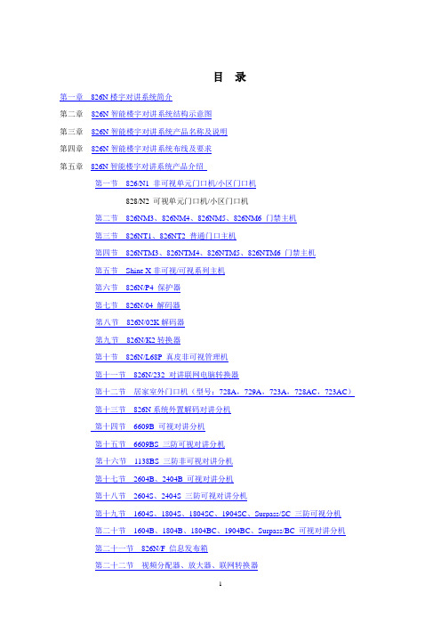
目录第一章826N楼宇对讲系统简介第二章826N智能楼宇对讲系统结构示意图第三章826N智能楼宇对讲系统产品名称及说明第四章826N智能楼宇对讲系统布线及要求第五章826N智能楼宇对讲系统产品介绍第一节826/N1 非可视单元门口机/小区门口机828/N2 可视单元门口机/小区门口机第二节826NM3、826NM4、826NM5、826NM6 门禁主机第三节826NT1、826NT2 普通门口主机第四节826NTM3、826NTM4、826NTM5、826NTM6 门禁主机第五节Shine X非可视/可视系列主机第六节826N/P4 保护器第七节826N/04 解码器第八节826N/02K解码器第九节826N/K2转换器第十节826N/L68P 真皮非可视管理机第十一节826N/232 对讲联网电脑转换器第十二节居家室外门口机(型号:728A,729A,723A,728AC,723AC)第十三节826N系统外置解码对讲分机第十四节6609B 可视对讲分机第十五节6609BS 三防可视对讲分机第十六节1138BS 三防非可视对讲分机第十七节2604B、2404B 可视对讲分机第十八节2604S、2404S 三防可视对讲分机第十九节1604S、1804S、1804SC、1904SC、Surpass/SC 三防可视分机第二十节1604B、1804B、1804BC、1904BC、Surpass/BC 可视对讲分机第二十一节826N/F 信息发布箱第二十二节视频分配器、放大器、联网转换器第二十三节Rs485四分支星型集线器826/L50—4第二十四节双绞线视频传输器第二十五节826N/K 转换器第二十六节789N/120、789N、789N/S电源系列第二十七节789N/120C 磁力锁控制板第二十八节826N/LX系列简易型数码主机第二十九节826N/LX系列二线入户型非可视对讲分机(2102、2112、2122)第三十节826N2/LX系列简易型数码可视对讲主机第三十一节826N2/LX系列四线加视频入户型可视对讲分机(6609L、2204L、2604L、2404L、1804L、1804LC、1604L)第三十二节9323型门禁控制板第三十三节826N/LDT—8多路交换机第三十四节SM6智能小区电脑管理软件第六章826N系统的命名方法以及配置方法第七章826N系统防静电、防雷设计第八章826N系统的优势于注意事项第五章826N智能化楼宇对讲系统产品介绍第一节826/N1 非可视单元门口机/小区门口机826/N2 可视单元门口机/小区门口机一、产品简介及外型组成部分826/N1,826/N2主机采用数码管显示方式,功能强大,性能稳定,各项功能均可通过键盘操作方便完成。
AZ826中文资料
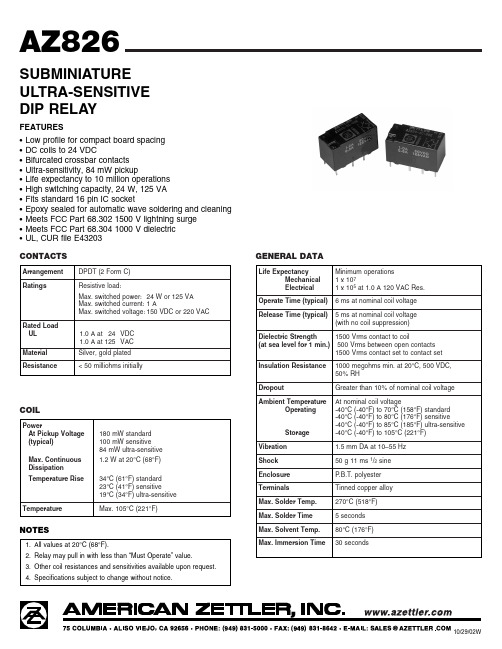
GENERAL DATALife ExpectancyMinimum operations Mechanical 1 x 10⁷Electrical 1 x 10⁵at 1.0 A 120 VAC Res.Operate Time (typical) 6 ms at nominal coil voltage Release Time (typical)5 ms at nominal coil voltage (with no coil suppression)Dielectric Strength 1500 Vrms contact to coil(at sea level for 1 min.)500 Vrms between open contacts1500 Vrms contact set to contact set Insulation Resistance 1000 megohms min. at 20°C, 500 VDC, 50% RHDropoutGreater than 10% of nominal coil voltage Ambient TemperatureAt nominal coil voltageOperating-40°C (-40°F) to 70°C (158°F) standard -40°C (-40°F) to 80°C (176°F) sensitive-40°C (-40°F) to 85°C (185°F) ultra-sensitive Storage-40°C (-40°F) to 105°C (221°F)Vibration 1.5 mm DA at 10–55 Hz Shock 50 g 11 ms 1/2sine Enclosure P.B.T. polyester TerminalsTinned copper alloy Max. Solder Temp.270°C (518°F)Max. Solder Time5 seconds Max. Solvent Temp.80°C (176°F)Max. Immersion Time30 secondsCOILPowerAt Pickup Voltage 180 mW standard (typical)100 mW sensitive 84 mW ultra-sensitive Max. Continuous 1.2 W at 20°C (68°F)Dissipation Temperature Rise34°C (61°F) standard 23°C (41°F) sensitive19°C (34°F) ultra-sensitive TemperatureMax. 105°C (221°F)CONTACTSArrangement DPDT (2 Form C)RatingsResistive load:Max. switched power:24 W or 125 VA Max. switched current:1 AMax. switched voltage:150 VDC or 220 VACRated Load UL 1.0 A at 24VDC 1.0 A at 125VAC Material Silver, gold plated Resistance< 50 milliohms initiallyULTRA-SENSITIVE DIP RELAYFEATURES •Low profile for compact board spacing •DC coils to 24 VDC•Bifurcated crossbar contacts •Ultra-sensitivity, 84 mW pickup•Life expectancy to 10 million operations •High switching capacity, 24 W, 125 VA •Fits standard 16 pin IC socket•Epoxy sealed for automatic wave soldering and cleaning •Meets FCC Part 68.302 1500 V lightning surge •Meets FCC Part 68.304 1000 V dielectric •UL, CUR file E43203NOTES1.All values at 20°C (68°F).2.Relay may pull in with less than “Must Operate ” value.3.Other coil resistances and sensitivities available upon request.4.Specifications subject to change without notice.RELAY ORDERING DATASTANDARD COIL SPECIFICATIONSNominal CoilMax. ContinuousCoil ResistanceMust OperateORDER NUMBERVDCVDC± 10%VDC 3 5.525 2.1AZ826-2C-3DME 59.270 3.5AZ826–2C –5DME 611.0100 4.2AZ826–2C –6DME 916.4225 6.3AZ826–2C –9DME 1221.94008.4AZ826–2C –12DME 2443.8160016.8AZ826–2C –24DMESENSITIVE COIL SPECIFICATIONSNominal CoilMax. ContinuousCoil ResistanceMust OperateORDER NUMBERVDCVDC± 10%VDC37.345 2.1AZ826-2C-3DSE 512.2125 3.5AZ826–2C –5DSE 614.7180 4.2AZ826–2C –6DSE 922.0405 6.3AZ826–2C –9DSE 1229.07208.4AZ826–2C –12DSE 2452.3288016.8AZ826–2C –24DSEULTRA-SENSITIVE COIL SPECIFICATIONSNominal CoilMax. ContinuousCoil ResistanceMust OperateORDER NUMBERVDCVDC± 10%VDC38.560 2.3AZ826–2C –3DSSE 4.512.7135 3.4AZ826–2C –4.5DSSE 514.2167 3.8AZ826–2C –5DSSE 617.0240 4.5AZ826–2C –6DSSE 925.4540 6.8AZ826–2C –9DSSE 1233.99609.0AZ826–2C –12DSSE 2467.9384018.0AZ826–2C –24DSSEMECHANICAL DATADimensions in inches with metric equivalents in parentheses. Tolerance: ± .010"。
1N829中文资料

Philips Semiconductors
Product specification
Voltage reference diodes
PACKAGE OUTLINE
1N821 to 1N829 1N821A to 1N829A
handbook, full pagewidth
0.55 max 1.6 max 25.4 min 3.04 max 25.4 min
1996 Mar 20
2Hale Waihona Puke 元器件交易网Philips Semiconductors
Product specification
Voltage reference diodes
ELECTRICAL CHARACTERISTICS Tj = 25 °C unless otherwise specified. SYMBOL Vref ∆Vref PARAMETER reference voltage reference voltage excursion 1N821; 1N821A 1N823; 1N823A 1N825; 1N825A 1N827; 1N827A 1N829; 1N829A SZ temperature coefficient 1N821; 1N821A 1N823; 1N823A 1N825; 1N825A 1N827; 1N827A 1N829; 1N829A rdif differential resistance 1N821 to 1N829 1N821A to 1N829A Notes IZ = 7.5 mA; see Fig.4 − − IZ = 7.5 mA: see Fig.3; notes 1 and 2 CONDITIONS IZ =7.5 mA IZ =7.5 mA; test points for Tamb: −55; +25; +75; +100 °C; see Fig.2; notes 1 and 2 MIN. 5.89 − − − − − − − − − −
MX-826中文资料
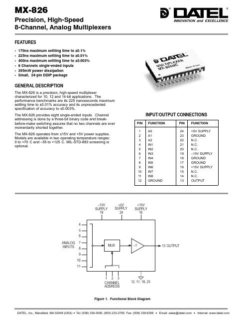
FEATURES•170ns maximum settling time to ±0.1%•225ns maximum settling time to ±0.01%•400ns maximum settling time to ±0.003%•8 Channels single-ended inputs •395mW power dissipation •Small, 24-pin DDIP packageGENERAL DESCRIPTIONThe MX-826 is a precision, high-speed multiplexercharacterized for 10, 12 and 14-bit applications. Theperformance benchmarks are its 225 nanoseconds maximum settling time to ±0.01% accuracy and its unprecedented specification of accuracy to ±0.003%.The MX-826 provides eight single-ended inputs. Channel addressing is done by a three-bit binary code and break-before-make switching assures that no two channels are ever momentarily shorted together.The MX-826 operates from ±15V and +5V power supplies.Models are available in two operating temperature ranges:0 to +70°C and –55 to +125°C. MIL-STD-883 screening is optional.PINFUNCTION PIN FUNCTION 1A024+5V SUPPLY 2A123GROUND 3A222N.C.4IN121N.C.5IN220N.C.6IN319–15V SUPPLY 7IN418GROUND 8IN517GROUND9IN616+15V SUPPLY 10IN715N.C.11IN814N.C.12GROUND13OUTPUTMX-826Precision, High-Speed8-Channel, Analog MultiplexersINNOVATION and EX C E LL E N C E®®Figure 1. Functional Block DiagramINPUT/OUTPUT CONNECTIONS456789101112, 17, 18, 2313OUTPUT+15V SUPPLY +5V SUPPLY ANALOG INPUTS CHANNEL ADDRESS15V SUPPLY DATEL, Inc., Mansfield, MA 02048 (USA) • Tel: (508) 339-3000, (800) 233-2765 Fax: (508) 339-6356 • Email: sales@ • Internet: 元器件交易网®®MX-826POWER REQUIREMENTS MIN TYP MAX UNITS Range+15V Supply +14.5+15+15.5Volts –15V Supply –14.5–15–15.5Volts +5V Supply+4.75+5+5.25Volts Current (Quiescent)+15V Supply —+13+21mA –15V Supply —–13–21mA +5V Supply—<1+1mA Power Supply Rejection Ratio 86——dB Power Dissipation—395575mWPHYSICAL/ENVIRONMMENTAL Operating Temp. Range, Case MC Model 0—+70°C MM Model–55—+125°C Storage Temp. Range –65—+150°CPackage Type 24-pin, metal-sealed, ceramic DDIPWeight0.42 oz. (12 grams)ABSOLUTE MAXIMUM RATINGSPARAMETERSLIMITS +15V Supply, Pin 160 to +18V –15V Supply, Pin 190 to –18V +5V Supply, Pin 24–0.5 to +7V Digital Inputs, Pins 1, 2, 3–0.3 to +5.5V Analog Inputs, Pins 4-11–15 to +15V Lead Temperature (10s)300°C Short Circuit to Ground , Pin 13ContinuousFUNCTIONAL SPECIFICATIONS(Apply over the operating temperature range and over the operating power supply range unless otherwise specified.)INPUTSMIN.TYP .MAX.UNITS Input Voltage Range±10±10.5—Volts Digital Input, Logic Levels Logic 1+2.0——Volts Logic 0——+0.8Volts Logic Loading Logic 1——+10µA Logic 0——–10µAOUTPUTSOutput Range ±10.0±10.5—Volts Output Current±15——mA Stable Capacitive Load 100——pF Output Impedance DC —0.1—OhmsPERFORMANCE Gain—–1—V/V Gain Error, 25°C ——±0.03%FS Gain Tempc o –55 to +125°C —±0.5±5ppm/°C Offset, 25°C—±0.1±0.5mV Offset Voltage Drift —<5±15µV/°C Slew Rate ±250±300—V/µs Cross Talk 100kHz —–90–83dB 1MHz —–80–75dB Bandwidth3dB Small Signal 88.5—MHz Full Power 3 4.5—MHz Input Impedance 2.45 2.5 2.55k ΩOutput Settling Time(10V step, +25°C) 500Ω Load ±0.1% 10 Bits —100170ns ±0.01% 12 Bits —150225ns ±0.003% 14 Bits—300400ns (20V step, + 25°C) 1k Ω Load ±0.1% 10 Bits —150200ns ±0.01% 12 Bits —200300ns ±0.003% 14 Bits—600720ns Switching Characteristics Break-Before-Make Delay 81525ns Turn On Time —2050ns Turn Off Time—2050ns Harmonic Distortion DC to 500kHz, 10Vp-p —–90–80dB Signal-to-Noise Ratio With Distortion —7269dB Without Distortion—8075dBTECHNICAL NOTES1.Bypass the ±15V and +5V power supplies with a 1µF, 25V tantalum electrolytic capacitors in parallel with a 0.1µF ceramic capacitors.2.Analog signals up to ±15V may be present while the MUX power supplies are off.3.The absence of an RON specification or output leakage specification is related to the architecture of the switching network. The inputs see a constant 2.5k Ohm input impedance whether the channel is on or off.4.Typical recovery time from an overvoltage condition of >±3V is approximately 200 nanoseconds from a negativeoverdrive and 700 nanoseconds from a positive overdrive.5.Double-level multiplexing may be used to provide up to 64channels (nine MX-826’s required).On MUX Address ChannelA2A1A010002001301040115100610171108111Table 1. Channel Addressing 元器件交易网元器件交易网MX-826®®MECHANICAL DIMENSIONSINCHES (mm)ORDERING INFORMATIONMODEL NO.CHANNELS OPER. TEMP. RANGEMX-826MC8SE0 to +70°CMX-826MM8SE–55 to +125°CMX-826/8838SE–55 to +125°CDESC drawing available: Drawing Number 5962-9450601.For MIL-STD-883 product specifications, contact DATEL.DATEL, Inc., Mansfield, MA 02048 (USA) • Tel: (508) 339-3000, (800) 233-2765 Fax: (508) 339-6356 • Email: sales@ • Internet: DATEL makes no representation that the use of its products in the circuits described herein, or the use of other technical information contained herein, will not infringe upon existing or future patent rights. The descriptions contained herein do not imply the granting of licenses to make, use, or sell equipment constructed in accordance therewith. Specifications are subject to change without notice. The DATEL logo is a registered DATEL, Inc. trademark.。
INA-02186中文资料

Low Noise, CascadableSilicon Bipolar MMIC Amplifier Technical DataFeatures•Cascadable 50 Ω Gain Block •Low Noise Figure:2.0 dB Typical at 0.5 GHz •High Gain:31 dB Typical at 0.5 GHz 26 dB Typical at 1.5 GHz • 3 dB Bandwidth:DC to 0.8 GHz •Unconditionally Stable (k>1)•Low Cost Plastic PackagePackage 84DescriptionThe INA-02184 and INA-02186 are low-noise silicon bipolar Mono-lithic Microwave IntegratedTypical Biasing ConfigurationINA-02184INA-02186Package 86V CCRF INRF OUTCircuit (MMIC) feedback amplifi-ers housed in low cost plasticpackages. They are designed for narrow or wide bandwidth commercial applications thatrequire high gain and low noise IF or RF amplification.The INA series of MMICs isfabricated using HP’s 10 GHz f T ,25 GHz f MAX , ISOSAT™-I silicon bipolar process which uses nitrideself-alignment, submicrometer lithography, trench isolation, ion implantation, gold metallization and polyimide intermetal dielec-tric and scratch protection to achieve excellent performance,uniformity and reliability.INA-02184, -02186 Absolute Maximum RatingsParameterAbsolute Maximum [1]Device Current50 mA Power Dissipation [2,3,4]400 mW RF Input Power+13 dBm Junction Temperature +150°C Storage Temperature–65 to 150°CThermal Resistance [2]: θjc = 90°C/W — INA-02184 θjc = 100°C/W — INA-02186Notes:1.Permanent damage may occur if any of these limits are exceeded.2.T CASE = 25°C.3.Derate at 11.1 mW/°C for T C >144°C for INA-02184.4.Derate at 10 mW/°C for T C > 110°C for INA-02186.G P Power Gain (|S 21|2) f = 0.5 GHz dB 29.031.029.031.0∆G P Gain Flatness f = 0.01 to 1.0 GHzdB ±2.0±2.0f 3 dB 3 dB Bandwidth [2]GHz 0.80.8ISO Reverse Isolation (|S 12|2)f = 0.01 to 1.0 GHz dB3939Input VSWR (Max over Freq. Range) f = 0.01 to 1.0 GHz 1.5 2.0Output VSWR (Max over Freq. Range) f = 0.01 to 1.0 GHz 1.7 1.7NF 50 Ω Noise Figuref = 0.5 GHz dB 2.0 2.0P 1 dB Output Power at 1 dB Gain Compression f = 0.5 GHz dBm 1111IP 3Third Order Intercept Point f = 0.5 GHz dBm 2323t D Group Delay f = 0.5 GHzpsec 330350V d Device VoltageV 4.05.57.04.05.57.0dV/dTDevice Voltage Temperature CoefficientmV/°C+10+10Notes:1.The recommended operating current range for this device is 30 to 40 mA. Typical performance as a function of current is on the following page.2.Referenced from 10 MHz Gain (G P ).INA-02184, -02186 Electrical Specifications [1], T A = 25°CSymbol Parameters and Test Conditions: I d = 35 mA, Z O = 50 ΩUnits Min.Typ.Max.Min.Typ.Max.VSWR INA-02184, -02186 Part Number Ordering InformationPart Number No. of DevicesContainer INA-02184-TR110007" Reel INA-02184-BLK 100Antistatic Bag INA-02186-TR110007" Reel INA-02186-BLK100Antistatic BagFor more information, see “Tape and Reel Packaging for Semiconductor Devices”.INA-02184 INA-02186INA-02184, -02186 Typical Performance, T A = 25°C(unless otherwise noted)1020304050I d (m A )G p (d B )I d (mA)V d (V)Figure 2. Device Current vs. Voltage.FREQUENCY (GHz)FREQUENCY (GHz)Figure 5. Output Power at 1 dB GainCompression vs. Frequency.Figure 6. Noise Figure vs. Frequency.N F (d B )15202530351.5.01.02.050.10.20.51.02.02.02.53.03.5G p (d B )N F (d B )FREQUENCY (GHz)Figure 1. Typical Gain and Noise Figure vs. Frequency, T A = 25°C, I d = 35 mA.152025303520304050Figure 3. Power Gain vs. Current.0.1 GHz 1.5 GHz1.0 GHz 0.5 GHz–55–25+25+85+125N F (d B )1.53.02.53.52.0P 1 d B (d B m )P 1 d B (d B m )G p (d B )TEMPERATURE (°C)Figure 4. Output Power and 1 dB Gain Compression, NF and Power Gain vs.CaseTemperature, f = 0.5 GHz, I d = 35 mA.FREQUENCY (GHz)Figure 7. Input VSWR vs. Frequency,I d = 35 mA.1.00:11.75:11.50:12.00:11.25:1FREQUENCY (GHz)Figure 8. Output VSWR vs. Frequency,I d = 35 mA.Typical INA-02184 Scattering Parameters (Z O = 50 Ω, T A = 25°C, I d = 35 mA)Freq.GHzMagAngdBMagAngdBMagAngMagAngk0.01.09–17631.939.33–1–40.0.0101.25–1 1.400.05.09–17131.939.24–6–41.9.008–12.25–4 1.660.10.10–16331.839.07–13–40.9.0091.25–8 1.520.20.13–15931.738.30–26–40.0.01015.23–13 1.440.30.15–16131.437.30–39–38.4.01216.22–17 1.290.40.18–16831.236.42–51–39.2.01132.21–15 1.390.50.19–17531.035.40–63–40.0.01034.21–16 1.520.60.2017930.734.20–75–37.1.01435.21–17 1.240.80.1916629.931.21–101–38.4.01238.24–26 1.441.00.1715928.426.36–126–36.5.01553.24–41 1.401.20.1515926.821.89–149–34.0.02056.22–60 1.311.40.1516324.817.36–169–33.2.02262.18–78 1.501.60.1616822.613.59175–31.4.02767.14–93 1.501.80.1816820.710.86161–31.1.02861.11–108 1.742.00.1916518.88.71149–30.2.03164.08–125 1.922.50.2315914.9 5.56127–29.1.03556.05–167 2.543.00.2715011.5 3.76106–27.1.04465.04156 2.893.50.301438.8 2.7489–26.0.05057.04137 3.394.00.33133 6.6 2.1473–25.0.05662.05137 3.78S 11S 21S 12 S 22Typical INA-02186 Scattering Parameters (Z O = 50 Ω, T A = 25°C, I d = 35 mA)Freq.GHzMagAngdBMagAngdBMagAngMagAngk0.01.09–17831.537.38–1–40.0.0101.24–1 1.460.05.09–17231.537.55–6–37.7.01311.24–5 1.220.10.11–16031.537.46–13–39.2.0118.23–9 1.370.20.14–15331.437.04–25–40.9.00915.22–17 1.600.30.18–15631.336.62–37–38.4.0121.21–25 1.300.40.22–16131.236.20–49–37.7.01328.19–30 1.250.50.25–16931.135.70–61–39.2.01142.18–35 1.400.60.28–17730.934.94–74–38.4.01244.16–39 1.330.80.3116530.232.34–101–36.5.01552.15–47 1.201.00.3014828.827.64–129–34.4.01957.12–59 1.151.20.2713527.022.26–153–32.4.02462.09–70 1.151.40.2412924.717.22–173–31.1.02861.07–80 1.231.60.2112822.513.27170–31.4.02762.04–82 1.521.80.2012920.410.42156–29.1.03561.02–83 1.502.00.2013118.48.34144–29.1.03563.01–20 1.792.50.2313314.5 5.29123–27.1.04459.0230 2.153.00.2713011.2 3.61103–25.7.05263.0227 2.563.50.311248.3 2.6086–24.4.06064.0234 2.974.00.34118 6.1 2.0270–23.4.06858.0130 3.28S 11S 21S 12 S 22Emitter Inductance and PerformanceAs a direct result of their circuit topology, the performance of INA MMICs is extremely sensitive to groundpath (“emitter”) induc-tance. The two stage design creates the possibility of a feed-back loop being formed through the ground returns of the stages. If the path to ground provided by the external circuit is “long” (high in impedance) compared to the path back through the ground return of the other stage, then instability can occur (see Fig. 1). This phenomena can show up as a “peaking” in the gain versus frequency response (perhaps creating a negative gain slope amplifier), an increase in input VSWR, or even as return gain (a reflection coefficient greater thanunity) at the input of the MMIC.The “bottomline” is that excellentgrounding is critical whenusing INA MMICs. The use ofplated through holes or equivalentminimal path ground returns atthe device is essential. Anappropriate layout is shown inFigure 2. A corollary is thatdesigns should be done on thethinnest practical substrate. Theparasitic inductance of a pair ofvia holes passing through 0.032"thick P.C. board is approximately0.1 nH, while that of a pair of viaholes passing through 0.062" thickboard is close to 0.5 nH. HP doesnot recommend using INA familyMMICs on boards thicker than32␣mils.These stability effects are entirelypredictable. A circuit simulationusing the data sheet S-parametersand including a description of theground return path (via model orequivalent “emitter” inductance)will give an accurate picture of theperformance that can be ex-pected. Device characterizationsare made with the ground leads ofthe MMIC directly contacting asolid copper block (systemground) at a distance of 2 to 4 milsfrom the body of the package.Thus the information in the datasheet is a true description of theperformance capability of theMMIC, and contains minimalcontributions from fixturing.Figure 1. INA PotentialGround Loop.Figure 2. INA Circuit Board 2x Actual Size.Package 84 DimensionsPackage 86 DimensionsDIMENSIONS ARE IN MILLIMETERS (INCHES)1.52 ± 0.25(0.060 ± 0.010)0.51 ±DIMENSIONS ARE IN MILLIMETERS (INCHES)。
INA168中文资料
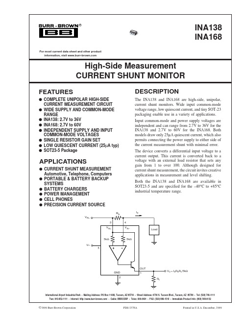
2
元器件交易网
PIN CONFIGURATION
TOP VIEW
OUT 1 GND 2
VI+N 3
5 V+ 4 VI–N
SOT
ABSOLUTE MAXIMUM RATINGS(1)
Supply Voltage, V+ INA138 ............................................................................... –0.3V to 60V INA168 ............................................................................... –0.3V to 60V
PARAMETER
CONDITION
INA138
MIN
TYP
MAX
MIN
INPUT Full-Scale Sense Voltage Common-Mode Input Range Common-Mode Rejection
Offset Voltage(1) vs Temperature vs Power Supply
Input common-mode and power supply voltages are independent and can range from 2.7V to 36V for the INA138 and 2.7V to 60V for the INA168. Both models draw only 25µA quiescent current, which also permits connecting the power supply to either side of the current measurement shunt with minimal error.
MIL-A-8625

MIL-A-8625F 2. 2.1 APPLICABLE DOCUMENTS Government documents.
2.1.1 Specifications and standards. The following specifications and standards form a part of this document to the extent specified herein. Unless otherwise specified, the issues of these documents are those listed in the issue of the Department of Defense Index of Specifications and Standards (DODISS) and supplement thereto, cited in the solicitation. SPECIFICATIONS MILITARY MIL-P-23377 MIL-C-81706 MIL-P-85582 FEDERAL QQ-A-250/4 STANDARDS FEDERAL FED-STD-141 FED-STD-151 MILITARY MIL-STD-105 Sampling Procedures and Tables For Inspection By Attribute Paint, Varnish, Lacquer, and Related Materials: Methods For Sampling and Testing Metals; Test Methods Aluminum Alloy 2024, Plate and Sheet Primer Coating, Epoxy-Polyamide, Chemical and Solvent Resistant Chemical Conversion Materials for Coating Aluminum and Aluminum Alloys Primer Coatings: Epoxy, Waterborne
826-22-014-00-001000;中文规格书,Datasheet资料
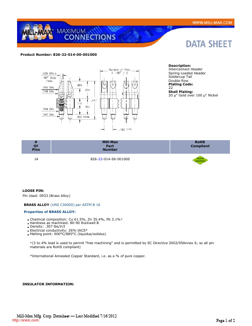
INSULATOR INFORMATION:
Mill-Max Mfg. Corp. Datasheet — Last Modified 7/16/2012
/
Page 1 of 2
NYLON 46 (Stanyl TE250F6 {30% glass} or TE250F9 {45% glass}, black) High Temperature Properties of NYLON 46: Brand: Stanyl Grade: TE250-F6 or F9 Material Heat Deflection Temp. (per ASTM D 648): 554°F (290°C) @ 264 psi Note: Materials above 446°F (230°C) are considered suitable for "eutectic" reflow soldering, above 500°F (260°C) for "lead-free" reflow soldering. Certificate of Compliance: This is to Certify that the product described above is manufactured to Mill-Max quality standards in accordance with all applicable specifications and drawing. Mill-Max certifies this product to be free from defects of materials and workmanship. This Certificate of Compliance covers the following requirements: Dimensional (all features verified to be within tolerances described on the applicable drawing). Raw Material (materials and properties verified to be as described on the applicable drawing). Plating (platings as required, thickness verified, and performance including solderability per mil-standard). Performance (insertion extraction or other force requirements as described on the applicable drawing).
MR826中文资料
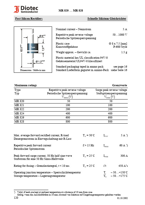
1)Valid, if leads are kept at ambient temperature at a distance of 10 mm from caseGültig, wenn die Anschlußdrähte in 10 mm Abstand von Gehäuse auf Umgebungstemperatur gehalten werden 12001.10.2002Fast Silicon RectifiersSchnelle Silizium GleichrichterNominal current – Nennstrom 5 ARepetitive peak reverse voltage 50…1000 V Periodische Spitzensperrspannung Plastic caseØ 8 x 7.5 [mm]KunststoffgehäuseP-600 StyleWeight approx. – Gewicht ca.1.5 gPlastic material has UL classification 94V-0Gehäusematerial UL94V-0 klassifiziertDimensions / Maße in mmStandard packaging taped in ammo pack see page 16Standard Lieferform gegurtet in Ammo-Pack siehe Seite 16Maximum ratings GrenzwerteType Typ Repetitive peak reverse voltage Periodische SpitzensperrspannungV RRM [V]Surge peak reverse voltage StoßspitzensperrspannungV RSM [V]MR 8205050MR 821100100MR 822200200MR 824400400MR 826600600MR 828800800Max. average forward rectified current, R-load T A = 50/C I FAV 5 A 1)Dauergrenzstrom in Einwegschaltung mit R-Last Repetitive peak forward current f > 15 Hz I FRM 60 A 1)Periodischer SpitzenstromPeak forward surge current, 50 Hz half sine-wave T A = 25/C I FSM 300 A Stoßstrom für eine 50 Hz Sinus-Halbwelle Rating for fusing – Grenzlastintegral, t < 10 ms T A = 25/Ci 2t 450 A 2s Operating junction temperature – Sperrschichttemperatur T j – 50…+150/C Storage temperature – LagerungstemperaturT S– 50…+175/C1)Valid, if leads are kept at ambient temperature at a distance of 10 mm from caseGültig, wenn die Anschlußdrähte in 10 mm Abstand von Gehäuse auf Umgebungstemperatur gehalten werden 12101.10.2002CharacteristicsKennwerteForward voltage – Durchlaßspannung T j = 25/C I F = 5 A V F < 1.2 V Leakage current – Sperrstrom T j = 25/CV R = V RRMI R < 25 :A Reverse recovery time I F = 0.5 A through/über t rr < 300 ns SperrverzugszeitI R = 1 A to/auf I R = 0.25 AThermal resistance junction to ambient airR thA< 20 K/W 1)Wärmewiderstand Sperrschicht – umgebende Luft。
INA826_中文资料

基本参数:输入共模范围:包括V型共模抑制比:104 dB, min (G = 10)100 dB, min at 5 kHz (G = 10)电源抑制比:100dB,最小(G=1)低失调电压:150μV,最大增益漂移:1 ppm/°C (G = 1), 35 ppm/°C (G > 1)噪音:18 nV/√Hz的,G≥100带宽:1 MHz (G = 1), 60 kHz (G = 100)受保护的输入高达±40 V电源电流:200μA电源电压范围:单电源:+2.7 V至+ 36V双电源:±1.35 V至±18 V规定温度范围:-40°C至+125°C封装:MSOP-8,SO-8和DFN-8{ 该INA826是一种低成本仪表放大器,提供极低的功耗和工作在一个很宽的单电源或双电源电压范围。
单个外部电阻设置为1的任何收益为1000,提供出色的温度稳定性,即使在g>的1,因为只有35 PPM/°C(最大值)的低增益漂移的结果。
该INA826经过优化,可提供超过100分贝(G =10)以上频率的出色的共模抑制比可达5千赫。
在G =1时,共模抑制比超过84分贝在整个输入共模范围从负电源一路攀升到正电源为1 V。
利用【Rail-to-Rai满摆幅(可以为输出,也可以为输入)】输出,该INA826是非常适合于低电压操作从2.7V单电源供电和双电源供电高达±18 V附加电路保护免受高达±40 V超出电源过压输入端通过限制输入电流至小于8毫安。
该INA826采用SO-8,MSOP-8和微小的3毫米×3毫米DFN-8表面贴装封装。
所有版本均工作在-40°C至+125°C温度范围。
}该INA826是一种低成本仪表放大器,提供极低的功耗和工作在一个很宽的单电源或双电源电压范围。
单个外部电阻设置任何增益为1 到1000。
INA826(低功耗宽电压RR仪放)
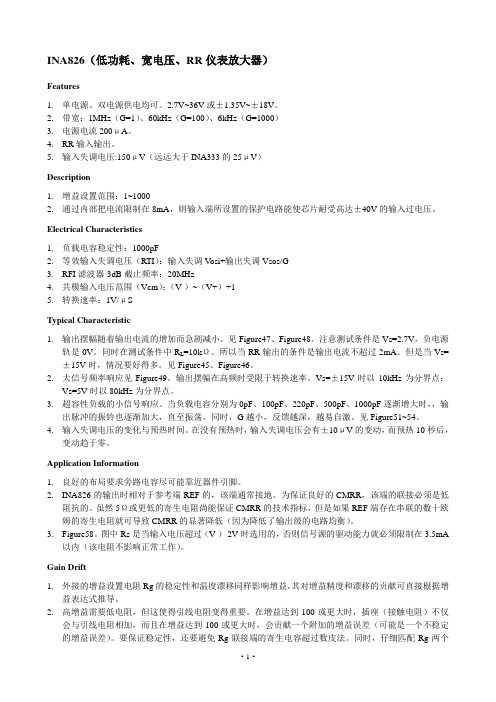
INA826(低功耗、宽电压、RR仪表放大器)Features1.单电源、双电源供电均可。
2.7V~36V或±1.35V~±18V。
2.带宽:1MHz(G=1)、60kHz(G=100)、6kHz(G=1000)3.电源电流200μA。
4.RR输入输出。
5.输入失调电压:150μV(远远大于INA333的25μV)Description1.增益设置范围:1~10002.通过内部把电流限制在8mA,则输入端所设置的保护电路能使芯片耐受高达±40V的输入过电压。
Electrical Characteristics1.负载电容稳定性:1000pF2.等效输入失调电压(RTI):输入失调V osi+输出失调Vsos/G3.RFI滤波器-3dB截止频率:20MHz4.共模输入电压范围(Vcm):(V-)~(V+)+15.转换速率:1V/μSTypical Characteristic1.输出摆幅随着输出电流的增加而急剧减小。
见Figure47、Figure48。
注意测试条件是Vs=2.7V,负电源轨是0V。
同时在测试条件中R L=10kΩ。
所以当RR输出的条件是输出电流不超过2mA。
但是当Vs=±15V时,情况要好得多。
见Figure45、Figure46。
2.大信号频率响应见Figure49。
输出摆幅在高频时受限于转换速率。
Vs=±15V时以10kHz为分界点;Vs=5V时以80kHz为分界点。
3.超容性负载的小信号响应。
当负载电容分别为0pF、100pF、220pF、500pF、1000pF逐渐增大时,,输出脉冲的振铃也逐渐加大,直至振荡。
同时,G越小,反馈越深,越易自激。
见Figure51~54。
4.输入失调电压的变化与预热时间。
在没有预热时,输入失调电压会有±10μV的变动,而预热10秒后,变动趋于零。
Application Information1.良好的布局要求旁路电容尽可能靠近器件引脚。
- 1、下载文档前请自行甄别文档内容的完整性,平台不提供额外的编辑、内容补充、找答案等附加服务。
- 2、"仅部分预览"的文档,不可在线预览部分如存在完整性等问题,可反馈申请退款(可完整预览的文档不适用该条件!)。
- 3、如文档侵犯您的权益,请联系客服反馈,我们会尽快为您处理(人工客服工作时间:9:00-18:30)。
基本参数:
输入共模范围:包括V型
共模抑制比:
104 dB, min (G = 10)
100 dB, min at 5 kHz (G = 10)
电源抑制比:100dB,最小(G=1)
低失调电压:150μV,最大
增益漂移:1 ppm/°C (G = 1), 35 ppm/°C (G > 1)
噪音:18 nV/√Hz的,G≥100
带宽:1 MHz (G = 1), 60 kHz (G = 100)
受保护的输入高达±40 V
电源电流:200μA
电源电压范围:
单电源:+2.7 V至+ 36V
双电源:±1.35 V至±18 V
规定温度范围:
-40°C至+125°C
封装:MSOP-8,SO-8和DFN-8
{ 该INA826是一种低成本仪表放大器,
提供极低的功耗和工作在一个很宽的单电
源或双电源电压范围。
单个外部电阻设置为
1的任何收益为1000,提供出色的温度稳
定性,即使在g>的1,因为只有35 PPM/°
C(最大值)的低增益漂移的结果。
该INA826经过优化,可提供超过100分贝
(G =10)以上频率的出色的共模抑制比可
达5千赫。
在G =1时,共模抑制比超过84
分贝在整个输入共模范围从负电源一路攀
升到正电源为1 V。
利用【Rail-to-Rai满摆
幅(可以为输出,也可以为输入)】输出,
该INA826是非常适合于低电压操作从2.7
V单电源供电和双电源供电高达±18 V
附加电路保护免受高达±40 V超出电源过
压输入端通过限制输入电流至小于8毫安。
该INA826采用SO-8,MSOP-8和微小的
3毫米×3毫米DFN-8表面贴装封装。
所有
版本均工作在-40°C至+125°C温度范
围。
}
该INA826是一种低成本仪表放大器,提供极低的功耗和工作在一个很宽的单电源或双电源电压范围。
单个外部电阻设置任何增益为1 到1000。
它提供了极好的温度稳定性,该INA826经过优化,可提供100dB以上(G=10)在频率高达5kHz的优良的共模抑制比。
在G =1时,共模抑制比从负电源超过84分贝在整个输入共模范围一路攀升到正电源的1V。
利用轨到轨输出,该INA826是非常适合于采用2.7V单电源低电压操作,以及双电源供电高达±18 V的附加电路,防止过压输入高达±40 V的超越电源通过限制输入电流至小于8毫安。
该INA826采用SO-8,MSOP-8和微小的3毫米×3毫米DFN-8表面贴装封装。
所有版本均工作在-40°C至+125°C温度范围。
引脚配置:
绝对值最大额定参数:
封装参数:
典型特性:
(1)输入补偿电压特性:(7)典型的误差漂移分布:
(2)输入补偿电压漂移特性:(8)典型的增益误差漂移分布:
(3)输出补偿电压特性:
(4)输出补偿电压漂移特性:
(5)输入偏置电流特性:
(6)输入补偿电流特性:
{在TA = + 25°C,VS =±15 V,RL = 10 kΩVREF = 0 V,和G = 1,除非另外标明}
应用信息:
(1)下图显示所需的基本连接INA826的操作。
好的布局实践要求,使用旁路电容放置尽可能接近器件引脚。
(2)INA826的输出被称为输出参考(REF)终端,这是通常接地。
这种连接必须是低阻抗的,以确保良好的共模抑制。
尽管5Ω或更小的电阻可以被承受,同时保持指定共模抑制比、十几个小的电阻与参考引脚串联,可以导致共模抑制比明显减小。
该电阻器是可选的,如果上面的输入电压保持(V–) – 2 V或信号源电流驱动能力仅限于小于 3.5mA,请看输入保护部分会有更多的细节描述。
设置增益:
INA826被设置为一个单一的外电路电阻,RG,连接引脚2和引脚3,它的值根据RG的选择可以概括为:
下表列出了几种常用的收益和电阻值。
的49.4kΩ的电阻在上面等式中是由两个内部24.7kΩ的
反馈电阻求和得到的。
这些片上电阻经过调整得到精确的绝对值。
这些电阻的精度和温度系数将影响INA826的增益精度和漂移参数。
运行电压:
INA826运作的供电范围+ 2.7 V至+ 36 V(±18±1.35 V)。
电源电压高超过40 V(±20 V)会对设备造成永久性损伤。
偏执微调:
内部电路:
输入偏置电流返回路径
低阻抗电平移动:。
