LINEAR LT3497 说明书
Agilent 34970A介绍

Sto/Rcl 3 選擇奇偶和數據位數
选择以下选项之一:“None(无)”(8 个数据位,出厂设
置)、“Even(偶
数)” (7 个数据位)或“Odd (奇数)” (7 个数据位)。
设 还2置可02奇以1E/7偶间V/1时接EN,设,7您置B数IST据位数。
14
三.儀器的使用
1.执行一次全面自
检。
进行选择时,该菜
单将自动指导您完成配置所选功能测量的所有相关选项。配置完参数之后,您将
:正在进行测量。
2021/7/1
9
• ADRS (寻址) :已对该仪器进行寻址设置,使其通过远程接口进行监听或通
• RMT (远程):仪器处于远程模式(远程接口)中。
VIEW
• ERROR(錯誤):已檢測到硬件或遠程接口錯誤,按
取錯誤
可以讀
• EXT (外部):已针对外部扫描时间间隔对该仪器SCA进N 行配置。
12
4.配置遠程接口
34970A 附带提供了 GPIB (IEEE-488) 接口和 RS-232 接口。一次仅可启用 一个接口,仪器出厂时已选择启用 GPIB 接口。
GPIB配置
shift Sto/Rcl 1 選擇GPIB接口
GPIB/488
Sto/Rcl 2 選擇GPIB 地址 您可以將儀器的地址設置為0至30之間的任一值,出廠設置的地址為”9”
ADDRESS 09
20S21to/7/R/1cl 3 保存所做更改并退出菜單
13
RS-232配置
shift Sto/Rcl 1 選擇RS-232接口
Sto/Rcl 2 選擇波特率
选择以下选项之一:1200, 2400, 4800, 9600, 19200, 38400, 57600 (出 厂设 置)或192101052B0A0 U波D特。
LinearLT三输出恒流源LED驱动方案

LinearLT三输出恒流源LED驱动方案部门: xxx时间: xxx整理范文,仅供参考,可下载自行编辑Linear LT3492三输出恒流源LED驱动方案关键词:电源管理,LED驱动器Linear 公司的LT3492是三输出DC/DC转换器,可用作恒流源LED驱动器,可工作在降压,升压和降升压模式. True Color PWM™调光的调光比高达3000:1,可调频率从330kHz 到2.1MHz,工作电压从3V 到30V,瞬间保护到40V,主要用于RGB照明,大显示屏,汽车和航空照明以及恒流源.本文介绍LT3492主要特性,方框图,以及多种应用电路图.The LTR3492 is a triple output DC/DC converter designed to operate as a constant-current source and is ideal for driving LEDs. The LT3492 works in buck, boost or buckboost mode. The LT3492 uses a fixed frequency, current mode architecture resulting in stable operation over a wide range of supply and output voltages. A frequency adjust pin allows the user to program switching frequency between330kHz and 2.1MHz to optimize efficiency and external component size.The external PWM input provides 3000:1 LED dimming on each channel. Each of the three channels has a built-in gate driver to drive an external LED-disconnect P-channel MOSFET, allowing high dimming range. The output current range of each channel of the LT3492 is programmed with an external sense resistor.The CTRL pin is used to adjust the LED current either for analog dimming orovertemperature protection.LT3492主要特性:True Color PWM™ Dimming Delivers Up to 3000:1 Dimming RatioBuilt-In Gate Driver for PMOS LED DisconnectThree Independent Driver Channels with 600mA, 60V Internal SwitchesOperates in Buck, Boost, Buck-Boost ModesCTRL Pin Accurately Sets LED Current Sense Threshold Over a Range of 10mV to 100mVAdjustable Frequency: 330kHz to 2.1MHzOpen LED ProtectionWide Input Voltage Range:Operation from 3V to 30VTransient Protection to 40VSurface Mount Components28-Lead (4mmx 5mm> QFN and TSSOP PackagesLT3492应用:RGB LightingBillboards and Large DisplaysAutomotive and Avionic LightingConstant-Current Sources图1.LT3492方框图:升压配置图2.高调光比三输出降压模式LED电源图3.最低BOM的降压模式LED驱动器图4.三路升压,100mAx12 LED驱动器图5. 双路升压LED驱动器图6.三路升压,100mAx9 LED驱动器:Vin控制调光图7.三路升压,100mAx12 LED驱动器图8.三路降模式LED驱动器:开路LED保护b5E2RGbCAP申明:所有资料为本人收集整理,仅限个人学习使用,勿做商业用途。
Agilent34970A按键中文说明
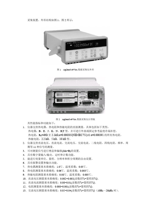
采集装置,外形结构如图1、图2所示:图1 Agilent34970A数据采集仪外形图2 Agilent34970A数据采集仪后背板其性能指标和功能如下:1.仪器支持热电偶、热电阻和热敏电阻的直接测量,具体包括如下类型:热电偶:B、E、J、K、N、R|T型,并可进行外部或固定参考温度冷端补偿。
热电阻:R0=49Ω至2.1kΩ,α=0.000385(NID/IEC751)或α=0.000391的所有热电阻。
热敏电阻:2.2 kΩ、5 kΩ、10 kΩ型。
2.仪器支持直流电压、直流电流、交流电压、交流电流、二线电阻、四线电阻、频率、周期等11种信号的测量。
3.可对测量信号进行增益和偏移(Mx+B)的设置。
4.具有数字量输入/输出、定时和计数功能。
5.能进行度量单位、量程、分辨率和积分周期的自由设置。
6.具有报警设置和输出功能。
7.热电偶测量基本准确度:1.0℃,温度系数:0.03℃。
8.热电阻测量基本准确度:0.06℃,温度系数:0.003℃。
9.热敏电阻测量基本准确度:0.08℃,温度系数:0.003℃。
10.直流电压测量基本准确度:0.002+0.005(读数的℅+量程的℅)。
11.直流电流测量基本准确度:0.08+0.01(读数的℅+量程的℅)。
12.电阻测量基本准确度:0.008+0.001(读数的℅+量程的℅)。
13.交流电压测量基本准确度:0.05+0.04(读数的℅+量程的℅)(10Hz~20kHz时)。
14. 交流电流测量基本准确度:0.1+0.04(读数的℅+量程的℅)(10Hz ~5kHz 时)。
15. 频率、周期测量基本准确度:0.01(读数的℅)(40Hz ~300kHz 时)。
16. 具有系统状态、校准设置和数据存储等功能。
1.2 Agilent34970A 数据采集仪的面板按钮功能与作用。
1.在所显示的通道上配置测量参数:● 在显示的通道上选择测量功能(直流电压、电阻等);● 选择温度测量的传感器类型;● 选择温度测量的单位(℃、℉、K );● 选择测量量程或自动量程设置;● 选择测量量程分辨率;● 将测量配置复制和粘贴到其它通道。
如何预防你的34970A数据采集器损坏

常用安捷伦仪表型号 34970A,34972A,34980A
1. 保证良好的接地措施
4. 注意检查仪表工作环境的温度和湿度
■ 请务必使用随机提供的带有地线的三线电源线;
■ 良好的接地措施可以避免静电的积累,从而避免静电 放电损坏仪表,同时也可以最大程度避免对操作人员 产生危险;
2. 注意仪表黄色警示标签的提示和 仪表测试范围
■ 仪表应该在清洁和干燥的环境中保存。温度要求 -20~70 °C,湿度小于 80%RH;
■ 如仪表装在机架中使用,应注意良好的通风。合适的 工作温度是 23 °C+/-5 °C,保证环境温度低于 35 °C;
■ 定期检查和清洁仪表通风口和风扇,保证良好的通风。
5. 请随时获取关于我们仪表的最新资料
■ 关于我们仪表的最新应用提示,请访问如下网址 /find/servicenotes
■ 或者通过如下网址给我们发 Email: /find/emailupdate
■ 查询维修服务中心信息请访问下面网址 /find/assist
3. 意避免输入超过允许范围的信号
■ 输入超过允许范围的信号将导致仪表输入通道损坏! 请 先将待测设备的输出信号调整到很小的安全范围后再 打开被测设备的信号源通路开关。这样可以避免由于 待测设备打开时的冲击而损坏仪表;
■ 避免带电拔插 线,先接GPIB 接线,再接电源线,再开机; 先关机,拔 电源线,再 拔 GPIB 线 ;
本文中的产品指标和说明可不经通知而更改 Agilent Technologies, Inc. 2008 出版号:5989-8787CHCN 2008 年 7 月 印于北京
■ 输入仪表的信号不能超过黄色警示标签所提示的范围;
34972A用户手册

设备构成1.34972A数据采集器2.34902A 16路模拟信号切换开关卡软件安装(不动脑缺省安装方式)1.先用USB线连接设备和计算机2.安装光盘1 IOSUITE16_3,即安装Agilent DATA IO 库文件等3.安装光盘2 Agilent benchlink 34830A 安装Agilent BenchLinkDatalogger和Agilent BenchLinkDatalogger Pro帮助视频1:1-Getting Started with Basic ScanningC:\Program Files\Agilent Technologies\Agilent BenchLinkDatalogger Pro\help\videos\GettingStartedwithBasicScanning.wmv帮助视颇2:2-Getting Started with Advanced FeaturesC:\Program Files\Agilent Technologies\Agilent BenchLinkDatalogger Pro\help\videos\ GettingStartedwithAdvancedFeatures.wmv帮助视颇3:C:\Program Files\Agilent Technologies\Agilent BenchLink DataLogger3\Help\On-Line\DLProVideo\BenchLinkDataLoggerPro.wmv重要帮助文件和手册"C:\ProgramFiles\Agilent\34972A\Documentation\34972-90001_Users_Guide.pdf"首先我们来认识前端面板前端面板有几组键分别选择不同的功能和操作其中有几个键下面有蓝色字体的具有Shift功能进行shift功能操作,按下shift键,这时屏幕右下角附近会有shift显示(持续显示约5秒),紧接着再按具有shift功能的键如果之前你按下了shift,想取消就再按一下shift键开盖接线图1热电偶2直流电压、交流电压、频率3两线制电阻、热电阻、热电偶4四线制电阻、热电阻5直流电流交流电流(仅21和22号接线端子构成1个测量通道,且只有34901A多通道卡具有该功能,最大测量电流1A,而34902A没有该功能(成光所为长光所配的是34902A),)对于34902A型16路模拟开关卡,4线制RTD测温,通道1接一对正负端(激励源通道),通道9再接一对正负端(探测通道)。
linear LT3757EDD 数据手册说明书
LT37571DESCRIPTIONDemonstration circuit 1548A features LT3757EDD in a 300kHz CUK converter circuit, designed for -15V output from a 7V to 28V in-put.The LT3757EDD operates over an input range of 2.9V to 40V, suitable for applications from single-cell lithium-ion battery portable electron-ics up to high voltage automotive and industrial power supplies. It also exhibits low shutdown quiescent current of 1µA, making them an ideal fit for battery-operated systems. Thanks to a novel FBX pin architecture, the LT3757EDD can be connected directly to a divider from either the positive output or the negative output to ground. It also packs many popular features such as soft-start, input undervoltage lockout, adjustablefrequency and synchronization in a small 10-lead MSOP package or a 3mm × 3mm QFN package.The LT3757EDD datasheet gives a complete description of the part, operation and application information. The datasheet must be read in con-junction with this quick start guide for demo cir-cuit 1548A.Design files for this circuit board are avail-able. Call the LTC factory.LT, LTC and are registered trademarks of Li-near Technology Corporation. All other trade-marks are the property of their respective own-ers.Table 1. Performance Summary for 300kHz CUK Regulator ( TA = 25oC ) PARAMETER CONDITION VALUE Minimum Input Voltage 7V Maximum Input Voltage 28V Output Voltage V OUT -15V +/-3%Maximum Output Current 1A Typical Switching Frequency 300kHzQUICK START PROCEDUREDemonstration circuit 1548A is easy to set up to evaluate the performance of the LT3757EDD. Refer to Figure 1 for proper measurement equipment setup and follow the procedure below:NOTE. When measuring the input or output volt-age ripple, care must be taken to avoid a long ground lead on the oscilloscope probe. Meas-ure the input or output voltage ripple by touch-ing the probe tip directly across the Vin or Vout and GND terminals. See Figure 2 for proper scope probe technique.1. Place JP1 on the ON position.2. Withpower off, connect the input power supply to Vin and GND.3. Turn on the power at the input.NOTE. Make sure that the input voltage doesnot exceed the maximum input voltage.4. Check for the proper output voltages.NOTE. If there is no output, temporarily dis-connect the load to make sure that the load is not set too high.Once the proper output voltages are estab-lished, adjust the loads within the operatingDEMO CIRCUIT 1548A QUICK START GUIDELT3757EDDHIGH EFFICIENCY CUK CONVERTER2 range and observe the output voltage regula-tion, ripple voltage, efficiency and other pa-rameters.Figure 1. Proper Measurement Equipment SetupFigure 2. Measuring Input or Output Ripple3。
34970A多点温度采集仪操作说明书

34970A多点温度采集仪操作说明书
一、目的
正确指导34970A多点温度采集仪的操作、使用、维护保养。
二、范围
本规程适用于本公司检验/生产过程中使用的34970A多点温度采集仪的操作
三、操作规范
3.1按实验内容的要求将上述传感器和信号引线接到规定通道的接线端,并拧紧固定。
具体方法如图1所示:
a.用一字螺丝刀拧开盖板螺丝。
b.将引线接到规定通道的接线端。
c.将引线沿槽绕出到出孔处。
d.重新盖好盖板并拧紧螺丝。
图1 模块接线图
3.2 将Agilent34901A测量模块插入Agilent34970A数据采集仪背部的最上面的槽中(即1#槽)。
如图2所示:
图1 模块安装图
拟制审核批准
日期日期日期。
Agilent34970A按键中文说明书

采集装置,外形结构如图1、图2所示:图1 Agilent34970A数据采集仪外形图2 Agilent34970A数据采集仪后背板其性能指标和功能如下:1.仪器支持热电偶、热电阻和热敏电阻的直接测量,具体包括如下类型:热电偶:B、E、J、K、N、R|T型,并可进展外部或固定参考温度冷端补偿。
热电阻:R0=49Ω至2.1kΩ,α=0.000385(NID/IEC751)或α=0.000391的所有热电阻。
热敏电阻:2.2 kΩ、5 kΩ、10 kΩ型。
2.仪器支持直流电压、直流电流、交流电压、交流电流、二线电阻、四线电阻、频率、周期等11种信号的测量。
3.可对测量信号进展增益和偏移(Mx+B)的设置。
4.具有数字量输入/输出、定时和计数功能。
5.能进展度量单位、量程、分辨率和积分周期的自由设置。
6.具有报警设置和输出功能。
7.热电偶测量根本准确度:1.0℃,温度系数:0.03℃。
8.热电阻测量根本准确度:0.06℃,温度系数:0.003℃。
9.热敏电阻测量根本准确度:0.08℃,温度系数:0.003℃。
10.直流电压测量根本准确度:0.002+0.005(读数的℅+量程的℅)。
11.直流电流测量根本准确度:0.08+0.01(读数的℅+量程的℅)。
12.电阻测量根本准确度:0.008+0.001(读数的℅+量程的℅)。
13.交流电压测量根本准确度:0.05+0.04(读数的℅+量程的℅)〔10Hz~20kHz时〕。
14.交流电流测量根本准确度:0.1+0.04(读数的℅+量程的℅)〔10Hz~5kHz时〕。
15.频率、周期测量根本准确度:0.01(读数的℅)〔40Hz~300kHz时〕。
16. 具有系统状态、校准设置和数据存储等功能。
1.2 Agilent34970A 数据采集仪的面板按钮功能与作用。
1.在所显示的通道上配置测量参数:● 在显示的通道上选择测量功能〔直流电压、电阻等〕;●选择温度测量的传感器类型;●选择温度测量的单位〔℃、℉、K 〕;●选择测量量程或自动量程设置;●选择测量量程分辨率;●将测量配置复制和粘贴到其它通道。
安捷伦数据采集器34970A产品说明

安捷伦数据采集器34970A产品说明安捷伦数据采集器34970A产品介绍:特性●3插槽主机,具有内置61/2 位数字万用表和8 种开关及控制插入式模块●可以测量和转换11种不同的输入信号: 温度(热电偶、rtd 和热敏电阻); 直流/ 交流电压、2 线和4 线电阻、频率和周期;直流/ 交流电流●1gbit lan、usb(34972a)、gpib 和rs-232 接口(34970a),可轻松连接至您的pc●图形web 界面,可以让您通过点击的方式执行监测和控制(34972a)●在没有pc的情况下,usb存储器支持下载配置和记录数据(34972a)●内含benchlink data logger软件,可配置和控制测试、显示测量结果以及收集数据,以便进行进一步分析无与伦比的价格和性能优势您可以将agilent 34970a和34972a数据采集/开关单元与目前市场上的其它数据采集系统做一个比较。
您就会发现很少有系统能够在测量性能、灵活性、连通性和易用性上与34970a/34972a 相匹敌—即便其成本可是它们的3 到5 倍。
如此经济的数据采集系统能够满足您什么样的期待? 您可以信任的测量在agilent 34970a/34972a里,我们将业界最经典的台式数字万用表作为测量引擎,嵌入到了它的3插槽主机箱内,并且该系统能够通过其紧凑的机箱提供具有内置信号调理功能的通用输入以及模块化的灵活性,特别是久经考验的安捷伦测量性能,这将使您收益良多。
它具有61/2位(22 比特) 分辨率,0.004% 的基本dcv 精度和超低的读数噪声。
与高达250通道/ 秒的扫描速率相结合,可为您提供所需的速度和精度,收到事半功倍的效果内置的信号调理功能, 助您及时完成任务无论您是需要测量温度、交流/ 直流电压、电阻、频率还是电流,34970a/34972a都能够胜任。
内置自动调节数字万用表可直接测量11 种不同功能,且无需进行昂贵的外部信号调理。
Agilent34970A按键中文说明

采集装置,外形结构如图1、图2所示:图1 Agilent34970A数据采集仪外形图2 Agilent34970A数据采集仪后背板其性能指标和功能如下:1.仪器支持热电偶、热电阻和热敏电阻的直接测量,具体包括如下类型:热电偶:B、E、J、K、N、R|T型,并可进行外部或固定参考温度冷端补偿。
热电阻:R0=49Ω至2.1kΩ,α=0.000385(NID/IEC751)或α=0.000391的所有热电阻。
热敏电阻:2.2 kΩ、5 kΩ、10 kΩ型。
2.仪器支持直流电压、直流电流、交流电压、交流电流、二线电阻、四线电阻、频率、周期等11种信号的测量。
3.可对测量信号进行增益和偏移(Mx+B)的设置。
4.具有数字量输入/输出、定时和计数功能。
5.能进行度量单位、量程、分辨率和积分周期的自由设置。
6.具有报警设置和输出功能。
7.热电偶测量基本准确度:1.0℃,温度系数:0.03℃。
8.热电阻测量基本准确度:0.06℃,温度系数:0.003℃。
9.热敏电阻测量基本准确度:0.08℃,温度系数:0.003℃。
10.直流电压测量基本准确度:0.002+0.005(读数的℅+量程的℅)。
11.直流电流测量基本准确度:0.08+0.01(读数的℅+量程的℅)。
12.电阻测量基本准确度:0.008+0.001(读数的℅+量程的℅)。
13.交流电压测量基本准确度:0.05+0.04(读数的℅+量程的℅)(10Hz~20kHz时)。
14. 交流电流测量基本准确度:0.1+0.04(读数的℅+量程的℅)(10Hz ~5kHz 时)。
15. 频率、周期测量基本准确度:0.01(读数的℅)(40Hz ~300kHz 时)。
16. 具有系统状态、校准设置和数据存储等功能。
1.2 Agilent34970A 数据采集仪的面板按钮功能与作用。
1.在所显示的通道上配置测量参数:● 在显示的通道上选择测量功能(直流电压、电阻等);● 选择温度测量的传感器类型;● 选择温度测量的单位(℃、℉、K );● 选择测量量程或自动量程设置;● 选择测量量程分辨率;● 将测量配置复制和粘贴到其它通道。
官方说明书LINEARLT3492说明书

LINEAR LT3492 Manual/file/2627659From collects and classifies the global productinstrunction manuals to help users access anytime andanywhere, helping users make better use of products.Home: / Chinese: /L DESIGN IDEASTriple Output LED Driver Works with Inputs to 60V and Delivers3000:1 PWM Dimming IntroductionThe LT3492 is a 60V triple outputLED driver for high input and/or highoutput voltage backlighting or directlighting applications. A single 4mm ×5mm IC can drive a large number ofLEDs, reducing overall solution costwhen compared to less capable drivers.A built-in gate driver for a disconnectPMOS in series with the LED string,along with other techniques, enablesa 3000:1 PWM dimming ratio. Whencoupled with the part’s analog dim-ming functions, the overall dimmingratio can be as high as 30,000:1. TheLT3492 can be configured into buck-mode, boost-mode or buck-boostmode, depending on the available in-put voltage source and the number andconfiguration of LEDs to be driven.High Input Voltage TripleBuck Mode LED DriverMany “regulated” supplies actuallyhave fairly loose tolerances. For ex-by Hua (Walker) BaiVFigure 1. Triple buck mode LED driver with open LED protectionVFigure 2. Triple boost mode 60mA × 14 LED driverDESIGN IDEAS L ample, a 48V supply can range between43V and 58V, well above most LEDdrivers’ safe operating voltage ratings.The LT3492’s 60V input voltage ratingmakes it an easy fit in such volatilevoltage environments.Figure 1 shows a triple buck-modeLED driver for high voltage inputs.Each channel can drive up to eight300mA white LEDs in series, a limitset by assuming 4V maximum forwardvoltage and a 43V minimum input volt-age. Red LEDs or infrared LEDs have much lower forward voltage, therefore each output can drive as many as 20 infrared LEDs. The V IN pin in Figure 1 is tied to a 5V supply, as opposed to PV IN, to improve circuit efficiency. Triple Boost Mode Driver Supports 14 LEDs per Output from a 9V–40V InputFigure 2 shows a triple boost mode LED driver that delivers 60mA to each LED string. Due to the LT3492’s 60V switch rating, each output can sup-port up to 14 LEDs. The 9V-to-40V input range covers a diverse range of applications, including regulated 12V, 24V, 32V to 36V, etc. Unlike in a buck mode regulator, where the output current capability is determined by the switch current limit, the current driving capability of a boost regulator is a function of the ratio of output volt-age to minimum input voltage. Figure3 shows the maximum output currentvs output voltage for a 9V minimuminput (assuming 85% efficiency at1MHz). For applications that requireless than 40V output, the LT3496should be considered instead.Triple Buck-Boost Mode LEDDriver Regulates During LoadDump EventsBuck-boost mode is used when theLED string voltage falls within theinput voltage range. Figure 4 shows abuck-boost application that uses oneinductor per driver. The LED stringis returned to the input—returningall LED strings to the same potentialallows easy heat sinking. To preventbody diode conduction, the drain ofthe disconnect PMOS is tied to theanode of the LED string. The high inputvoltage of the circuits in Figure 2 andFigure 4 is a real benefit in automotiveapplications, where the ability to ridethrough 40V load dump events whilemaintaining LED current regulation isrequired. Figure 5 shows the greaterthan 3000:1 PWM dimming ratioachievable with the LT3492. This highPWM dimming ratio helps improve thepicture quality of an LCD display undervarious dynamic conditions.ConclusionThe LT3492 is a high voltage tripleoutput LED driver with 60V ratedswitches, allowing high input voltageand/or high output voltage operationswith accurate LED current. It can runin buck mode, boost mode or buck-boost mode with 3000:1 PWM dimmingcapability. LPWM5V/DIV0V0VI LED50mA/DIV1µs/DIVFigure 5. High dimming ratio (>3000:1)improves quality of an LCD displayV4 LEDs1150k20kOVP3M3Figure 4. Triple buck-boost mode 150mA × 4 LED driver35030025020015010050OUTPUT VOL TAGE (V)OUTPUTCURRENT(mA)Figure 3. Maximum output currentcapability of an LT3492 boost circuit。
linear LT3495, LT3495B, LT3495-1, AND LT3495B-1 Qu
LT3495, LT3495B, LT3495-1, AND LT3495B-1 DESCRIPTIONDem onstrati on ci rcui ts 1219A-A, -B, -C and -D are M i cropow er Low Noi se Boost Converters W i th Output Di sconnect f eaturi ng the f our di f f erent Lt3495 versi ons: LT3495, LT3495B, LT3495-1, and LT3495B-1. Al l ver-si ons convert a 3V-6V source to 15V. The –A and -B ver-si ons suppl y 75m A at 3Vi n w hi l e the -C and -D suppl y 36m A. The –A and –C versi ons f eature the LT3495EDDB and the LT3495EDDB-1 respecti vel y, w hi ch have non-audi bl e sw i tchi ng f requency over the enti re l oad range. Al l LT3495 versi ons f eature a l ow noi se control schem e, i ntegrated output di sconnect f uncti on, di m m i ng control , and si ngl e output sense resi stor. These ci rcui ts are i n-tended f or space-consci ous appl i cati ons such as OLEDpow er, M P3 Pl ayers, and Low Noi se Bi as Suppl i es. The LT3495 datasheet gi ves a com pl ete descri pti on of the parts, operati on and appl i cati on i nf orm ati on. The datasheet m ust be read i n conj uncti on w i th thi s qui ck start gui de f or w orki ng on or m odi f yi ng the dem o ci rcui t 1219.Design files for this circuit board are available. Call the LTC factory.L , LTC, LTM , LT are regi stered tradem arks of Li near Technol ogy Corporati on.PERF ORM A NCE SU M M A RY F OR DC1219A -A /L T3495 A ND DC1219A -B /L T3495B Specifications are at TA = 25°CSYM BOL PARAM ETERCONDI TI ONSM I NTYP M AX UNI TSV I N I nput Suppl y Range3 6 V V OUT Output Vol tage Range V I N = 3.6V, I LOAD = 75m A 14.6 15 15.4 V V OUTOutput Vol tage Range V I N = 6V, I LOAD = 75m A 14.6 15 15.4 V RI PPLEV I N = 3.6V, I LOAD = 75m A 10 m V EFFI CI ENCY Load at Vout V I N = 3.6V, I LOAD = 75m A 80.5 %EFFI CI ENCYLoad at VoutV I N = 6V, I LOAD = 75m A83.5 %PERF ORM A NCE SU M M A RY F OR DC1219A -C/L T3495-1 A ND DC1219A -D/L T3495B -1 Specifications are at TA = 25°CSYM BOL PARAM ETERCONDI TI ONSM I NTYP M AX UNI TSV I N I nput Suppl y Range3 6 V V OUT Output Vol tage Range V I N = 3.6V, I LOAD = 36m A 14.6 15 15.4 V V OUTOutput Vol tage Range V I N = 6V, I LOAD = 36m A 14.6 15 15.4 V RI PPLEV I N = 3.6V, I LOAD = 36m A 10 m V EFFI CI ENCY Load at Vout V I N = 3.6V, I LOAD = 36m A 82.5 %EFFI CI ENCYLoad at VoutV I N = 6V, I LOAD = 36m A84.5 %DEMO C IR C U IT 1219Q U IC K S TA R T G U IDEL T 3495, L T 3495B , L T 3495-1, a n dL T 3495B -1Mic ro p o w e r L o w N o ise B o o st C o n v e rte rs W ith Ou tp u tDisc o n n e c tLT3495, LT3495B, LT3495-1, AND LT3495B-1 Q U ICK STA RT PROCEDU REDem onstrati on ci rcui t 1219 i s easy to set up to eval uate the perf orm ance of the LT3495, LT3495B, LT3495-1, and LT3495B-1. Ref er to Fi gure 1 f or proper m easurem ent equi pm ent setup and f ol l ow the procedure bel ow :NOTE. W hen m easuri ng the i nput or output vol tage ri ppl e, care m ust be taken to avoi d a l ong ground l ead on the osci l l oscope probe. M easure the i nput or output vol tage ri ppl e by touchi ng the probe ti p di rectl y across the Vi n or Vout and GND term i nal s. See Error! Reference source not found. f or proper scope probe techni que.1. Pl ace j um pers i n the f ol l ow i ng posi ti ons: JP1 - Run2. W i th pow er of f , connect the i nput pow er suppl y toVi n and GND. 3. Turn on the pow er at the i nput.Check f or the proper output vol tages. Vout = 14.6V to 15.4V.NOTE. I f there i s no output, tem porari l y di sconnect the l oad to m ake sure that the l oad i s not set too hi gh.4. Once the proper output vol tage i s establ i shed, ad-j ust the l oad w i thi n the operati ngrange and ob-serve the output vol tage regul ati on, ri ppl e vol tage, ef f i ci ency and other param eters.Figure 1. Proper M easurem ent Equipment SetupFigure 2. M easuring I nput or output RippleLT3495, LT3495B, LT3495-1, AND LT3495B-1。
Agilent-34972A操作说明精选全文完整版
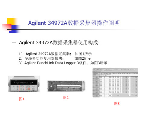
一.Agilent 34972A数据采集器使用构成:
1) Agilent 34972A数据采集器; 如图1所示 2)多路多功能复用器模块; 如图2所示 3)Agilent BenchLink Data Logger 3软件;如图3所示
图1
图2
图3
Agilent 34972A数据采集器操作阐明
1) Agilent 34972A数据采集器 选择配置参数:Measure键+旋钮(配合使用)
在所显示旳通道上配置测量参数: ● 在显示旳通道上选择测量功能(温度、电压、电阻、电流、频率等); ● 选择温度测量旳传感器类型; ● 选择温度测量旳单位(℃、℉、K); ● 选择测量量程或自动量程设置; ● 选择测量量程辨别率;
导出数据
Agilent 34972A数据采集器操作阐明
导出旳数据成果,仅供参照!
谢谢! 2023-1-18
示精度0.1 ℃)。 7.再按Measure键,即可完毕设置并退出。
其他各通道配置类似上述操作,详细环节略。 8. 配置各通道后,按Scan按钮开始扫描。 9. 按View按钮,再经过旋转旋扭,直到显示屏出现READINGS (读数)。 10. 按View按钮(表达拟定),即可在显示屏上看到刚刚扫描得到旳读数,经过旋转旋扭,能够看到各
电偶)。 4..再按Measure键(表达拟定并继续设置),再经过旋转旋扭,直到显示屏出现J TYPE T/C(J型热
电偶,并带冷端补偿)。 5.再按Measure键(表达拟定并继续设置),再经过旋转旋扭,直到显示屏出现UNITS ℃ (度量单
位为摄氏度)。 6.再按Measure键(表达拟定并继续设置),再经过旋转旋扭,直到显示屏出现DISPLAY 0.1 ℃(显
LINEAR TECHNOLOGY LTC1734 说明书
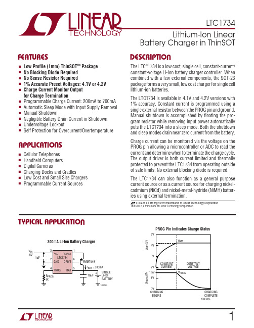
1234564.2V (2.5V at amplifier A1’s input) the amplifier will divert current away from the output driver thus limiting charge current to that which will maintain 4.2V on the battery. This is the constant voltage mode.When in the constant voltage mode, the 1000:1 current ratio is still valid and the voltage on the PROG pin will indicate the charge current as a proportion of the maxi-mum current set by the current programming resistor.The battery charge current is 1000 • (V PROG /R PROG ) amps.This feature allows a microcontroller with an ADC to easily monitor charge current and if desired, manually shut down the charger at the appropriate time.When V CC is applied, the charger can be manually shut down by floating the otherwise grounded end of R PROG .An internal 3µA current source pulls the PROG pin above the 2.15V threshold of voltage comparator C1 initiating shutdown.For charging NiMH or NiCd batteries, the LTC1734 can function as a constant current source by grounding the BAT pin. This will prevent amplifier A1 from trying to limit charging current and only A2 will control the current.Fault conditions such as overheating of the die or exces-sive DRIVE pin current are monitored and limited.When input power is removed or manual shutdown is entered, the charger will drain only tiny leakage currents from the battery, thus maximizing battery standby time.With V CC removed the external PNP’s base is connected to the battery by the charger. In manual shutdown the base is connected to V CC by the charger.OPERATIOUThe LTC1734 is a linear battery charger controller. Opera-tion can best be understood by referring to the Block Diagram. Charging begins when V CC rises above the UVLO (Undervoltage Lockout) threshold V UVLOI and an external current programming resistor is connected be-tween the PROG pin and ground. When charging, the collector of the external PNP provides the charge current.The PNP’s emitter current flows through the I SENSE pin and through the internal 0.06Ω current sense resistor.This current is close in magnitude, but slightly more than the collector current since it includes the base current.Amplifier A3, along with the P-channel FET, will force the same voltage that appears across the 0.06Ω resistor to appear across the internal 60Ω resistor. The scale factor of 1000:1 in resistor values will cause the FET’s drain current to be 1/1000 of the charge current and it is this current that flows through the PROG pin. In the constant current mode, amplifier A2 is used to limit the charge current to the maximum that is programmed by R PROG .The PROG pin current, which is 1/1000 of the charge current, develops a voltage across the program resistor.When this voltage reaches 1.5V, amplifier A2 begins diverting current away from the output driver, thus limit-ing the charge current. This is the constant current mode.The constant charge current is 1000 • (1.5V/R PROG ).As the battery accepts charge, its voltage rises. When it reaches the preset float voltage of 4.2V (LTC1734-4.2version), a precisely divided down version of this voltage (2.5V) is compared to the 2.5V internal reference voltage by amplifier A1. If the battery voltage attempts to exceedAPPLICATIO S I FOR ATIOW UUU Charging OperationCharging begins when an input voltage is present that exceeds the undervoltage lockout threshold (V UVLOI ), a Li-Ion battery is connected to the charger output and a program resistor is connected from the PROG pin to ground. During the first portion of the charge cycle, when the battery voltage is below the preset float voltage, the charger is in the constant current mode. As the battery voltage rises and reaches the preset float voltage, thecharge current begins to decrease and the constant voltage portion of the charge cycle begins. The charge current will continue to decrease exponentially as the battery approaches a fully charged condition.Should the battery be removed during charging, a fast built-in protection circuit will prevent the BAT pin from ris-ing above 5V, allowing the precision constant voltage circuit time to respond.789Monitoring Charge CurrentThe voltage on the PROG pin indicates the charge current as a proportion of the maximum current set by the program resistor. The charge current is equal to 1000 •(V PROG /R PROG ) amps. This feature allows a microcontrol-ler with an ADC to easily monitor charge current and if desired, manually shut down the charger at the appropri-ate time. See Figure 1 for an example. The minimum PROG pin current is about 3µA (I PROGPU ).Errors in the charge current monitor voltage on the PROG pin are inversely proportional to battery current and can be statistically approximated as follows:One Sigma Error(%) ≅ 1 + 0.3/I BAT (A)Dynamic loads on the battery will cause transients to appear on the PROG pin. Should they cause excessive errors in charge current monitoring, a simple RC filter as shown in Figure 2 can be used to filter the transients. The filter will also quiet the PROG pin to help prevent inadvert-ent momentary entry into the manual shutdown mode.Because the PROG pin is in a closed-loop signal path the pole frequency must be kept high enough to maintain adequate AC stability. This means that the maximum resistance and capacitance presented to the PROG pin must be limited. See the Stability section for more details.Constant Current SourceThe LTC1734 can be used as a constant current source by disabling the voltage control loop as shown in Figure 3.This is done by pulling the BAT pin below the preset float voltages of 4.1V or 4.2V by grounding the BAT pin. The program resistor will determine the output current. The output current range can be between approximately 50mA and 700mA, depending on the maximum power rating of the external PNP pass transistor.External PNP TransistorThe external PNP pass transistor must have adequate beta, low saturation voltage and sufficient power dissipa-tion capability (including any heat sinking, if required).To provide 700mA of charge current with the minimum available base drive of approximately 30mA requires a PNP beta greater than 23. If lower beta PNP transistors areused, more base current is required from the LTC1734.This can result in the output drive current limit being reached, or thermal shutdown due to excessive power dissipation. Excessive beta can affect AC stability (see Stability section)With low supply voltages, the PNP saturation voltage (V CESAT ) becomes important. The V CESAT must be less than the minimum supply voltage minus the maximum voltage drop across the internal sense resistor and bond wires (0.1Ω) and battery float voltage. If the PNP transis-tor can not achieve the low saturation voltage required,base current will dramatically increase. This is to be avoided for a number of reasons: output drive may reach current limit resulting in the charger’s characteristics to go out of specifications, excessive power dissipation may force the IC into thermal shutdown, or the battery could become discharged because some of the current from the DRIVE pin could be pulled from the battery through the forward biased collector base junction.For example, to program a charge current of 500mA with a minimum supply voltage of 4.75V, the minimum operat-ing V CE is:V CE(MIN)(V) = 4.75 – (0.5)(0.1) – 4.2 = 0.5V The actual battery charge current (I BAT ) is slightly smaller than the expected charge current because the charger senses the emitter current and the battery charge current will be reduced by the base current. In terms of β (I C /I B ),I BAT can be calculated as follows:I BAT (A) = 1000 • I PROG [β/(β + 1)]If β = 50, then I BAT is 2% low. If desired, the 2% loss can be compensated for by increasing I PROG by 2%.Another important factor to consider when choosing the PNP pass transistor is the power handling capability. The transistor’s data sheet will usually give the maximum rated power dissipation at a given ambient temperature with a power derating for elevated temperature operation. The maximum power dissipation of the PNP when charging is:P D(MAX)(W) = I BAT (V DD(MAX) – V BAT(MIN))V DD(MAX) is the maximum supply voltage and V BAT(MIN) is the minimum battery voltage when discharged.APPLICATIO S I FOR ATIO W UU U10Once the maximum power dissipation and V CE(MIN) are known, Table 1 can be used as a guide in selecting some PNPs to consider. In the table, very low V CESAT is less than 0.25V, low V CESAT is 0.25V to 0.5V and the others are 0.5V to 0.8V all depending on the current. See the manufacturer’s data sheet for details. All of the PNP transistors are rated to carry at least 1A continuously as long as the power dissipation is within limits. The Stability section addresses caution in the use of high beta PNPs.Should overheating of the PNP transistor be a concern,protection can be achieved with a positive temperature coefficient (PTC) thermistor, wired in series with the current programming resistor and thermally coupled to the transistor. The PTH9C chip series from Murata has a steep resistance increase at temperature thresholds from 85°C to 145°C making it behave somewhat like a thermo-stat switch. For example, the model PTH9C16TBA471Q thermistor is 470Ω at 25°C, but abruptly increase its resistance to 4.7k at 125°C. Below 125°C, the device exhibits a small negative TC. The 470Ω thermistor can be added in series with a 1.6k resistor to form the current programming resistor for a 700mA charger. Should the thermistor reach 125°C, the charge current will drop to 238mA and inhibit any further increase in temperature.StabilityThe LTC1734 contains two control loops: constant voltage and constant current. To maintain good AC stability in theconstant voltage mode, a capacitor of at least 4.7µF is usually required from BAT to ground. The battery and interconnecting wires appear inductive at high frequen-cies, and since these are in the feedback loop, this capaci-tance may be necessary to compensate for the inductance.This capacitor need not exceed 100µF and its ESR can range from near zero to several ohms depending on the inductance to be compensated. In general, compensation is optimal with a capacitance of 4.7µF to 22µF and an ESR of 0.5Ω to 1.5Ω.Using high beta PNP transistors (>300) and very low ESR output capacitors (especially ceramic) reduces the phase margin, possibly resulting in oscillation. Also, using high value capacitors with very low ESRs will reduce the phase margin. Adding a resistor of 0.5Ω to 1.5Ω in series with the capacitor will restore the phase margin.In the constant current mode, the PROG pin is in the feedback loop, not the battery. Because of this, capaci-tance on this pin must be limited. Locating the program resistor near the PROG pin and isolating the charge current monitoring circuitry (if used) from the PROG pin with a 1k to 10k resistor may be necessary if the capaci-tance is greater than that given by the following equation:C k R MAX pF PROG()=400APPLICATIO S I FOR ATIO W UU U Table 1. PNP Pass Transistor Selection GuideMaximum P D (W)Mounted on Board at T A = 25°CPackage Style ZETEX Part NumberROHM Part NumberComments 0.5SOT-23FMMT549Low V CESAT0.625SOT-23FMMT720Very Low V CESAT, High Beta1SOT-89FCX589 or BCX691.1SOT-23-6ZXT10P12DE6Very Low V CESAT, High Beta, Small 1 to 2SOT-89FCX717Very Low V CESAT, High Beta 2SOT-223FZT589Low V CESAT2SOT-223BCP69 or FZT5490.75FTR 2SB822Low V CESAT 1ATV 2SB1443Low V CESAT 2SOT-892SA1797Low V CESAT10 (T C = 25°C)TO-2522SB1182Low V CESAT, High Beta11LTC1734Information furnished by Linear Technology Corporation is believed to be accurate and reliable.However, no responsibility is assumed for its use. Linear Technology Corporation makes no represen-tation that the interconnection of its circuits as described herein will not infringe on existing patent rights.Figure 5. Stability WaveformsSHUT DOWNDELAY CONSTANT CURRENTHORIZONTAL SCALE: 100µs/DIVCONSTANT VOLTAGE12LTC1734© LINEAR TECHNOLOGY CORPORA TION 2001sn1734 1734fs LT/TP 0801 2K • PRINTED IN THE USALinear Technology Corporation1630 McCarthy Blvd., Milpitas, CA 95035-7417(408) 432-1900 q FAX: (408) 434-0507 q 。
34970A数据采集器中文说明书
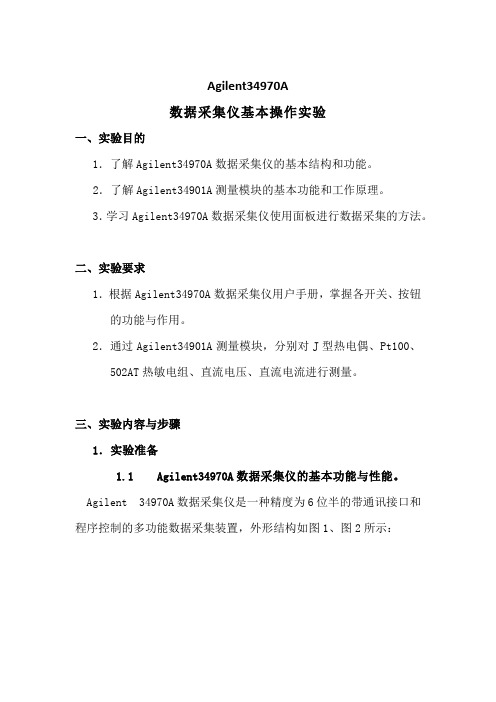
Agilent34970A数据采集仪基本操作实验一、实验目的1.了解Agilent34970A数据采集仪的基本结构和功能。
2.了解Agilent34901A测量模块的基本功能和工作原理。
3.学习Agilent34970A数据采集仪使用面板进行数据采集的方法。
二、实验要求1.根据Agilent34970A数据采集仪用户手册,掌握各开关、按钮的功能与作用。
2.通过Agilent34901A测量模块,分别对J型热电偶、Pt100、502AT热敏电组、直流电压、直流电流进行测量。
三、实验内容与步骤1.实验准备1.1 Agilent34970A数据采集仪的基本功能与性能。
Agilent 34970A数据采集仪是一种精度为6位半的带通讯接口和程序控制的多功能数据采集装置,外形结构如图1、图2所示:其性能指标和功能如下:1.仪器支持热电偶、热电阻和热敏电阻的直接测量,具体包括如下类型:热电偶:B、E、J、K、N、R|T型,并可进行外部或固定参考温度冷端补偿。
热电阻:R0=49Ω至 2.1kΩ,α=0.000385(NID/IEC751)或α=0.000391的所有热电阻。
热敏电阻:2.2 kΩ、5 kΩ、10 kΩ型。
2.仪器支持直流电压、直流电流、交流电压、交流电流、二线电阻、四线电阻、频率、周期等11种信号的测量。
3.可对测量信号进行增益和偏移(Mx+B)的设置。
4.具有数字量输入/输出、定时和计数功能。
5.能进行度量单位、量程、分辨率和积分周期的自由设置。
6.具有报警设置和输出功能。
7.热电偶测量基本准确度:1.0℃,温度系数:0.03℃。
8.热电阻测量基本准确度:0.06℃,温度系数:0.003℃。
9.热敏电阻测量基本准确度:0.08℃,温度系数:0.003℃。
10.直流电压测量基本准确度:0.002+0.005(读数的℅+量程的℅)。
11.直流电流测量基本准确度:0.08+0.01(读数的℅+量程的℅)。
安捷伦34970A操作规范
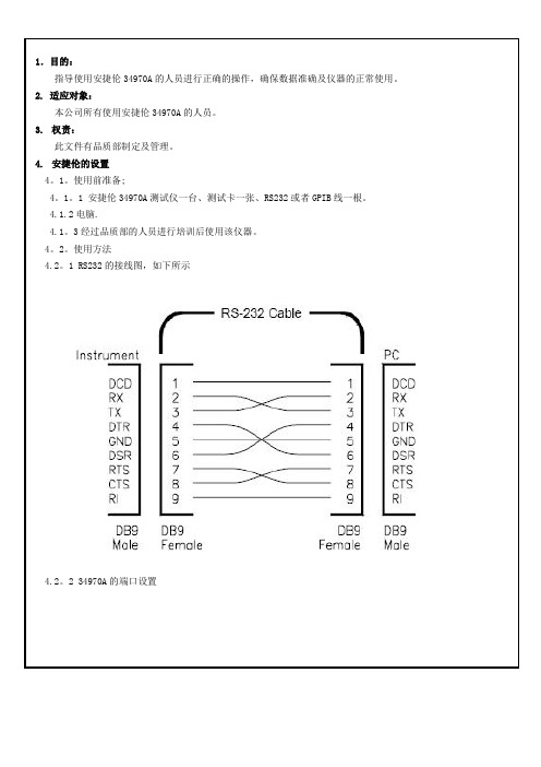
1.目的:指导使用安捷伦34970A的人员进行正确的操作,确保数据准确及仪器的正常使用。
2. 适应对象:本公司所有使用安捷伦34970A的人员。
3.权责:此文件有品质部制定及管理。
4.安捷伦的设置4。
1。
使用前准备;4。
1。
1 安捷伦34970A测试仪一台、测试卡一张、RS232或者GPIB线一根。
4.1.2电脑.4.1。
3经过品质部的人员进行培训后使用该仪器。
4。
2。
使用方法4.2。
1 RS232的接线图,如下所示4.2。
2 34970A的端口设置确认电脑COM口设置,注意一定要保证电脑的COM设置和34970A RS—232设置一致!4.2.3 电脑端口设置第一步:在控制面板中打开系统属性对话框(for WinXP)第二步:打开硬件管理器第三步:检查并修改COM设置,使其和34970A RS-232设置一致4。
2.4 GPIB的通讯线使用方法第一步:电脑开机后连接GPIB通讯线,按照步骤安装GPIB的驱动第二步:修改安捷伦34970A的参数设置,参照使用RS232的步骤,选择GPIB即可第三步:安捷伦34970A参数设置完成后即可进行联机,进行温度、电压、电流的采集。
5.软件设置第一步:点击“配置仪器”如果有仪器存在,先点击“删除仪器"。
点击“添加仪器”,然后点击“查找”查找到仪器后,点击“连接",即可连上电脑第二步:点击“配置通道”将所需要的通道号进行选择,并选择相应的功能。
测量直流电压时,选择“直流电压";测量温度时,选择相应类型的热电偶.以使用K型热电偶进行温度测量为例,如下所示:第三步:点击“扫描和记录数据”点击“扫描和记录数据”,如下所示。
并点击选择框内的设置,进行相关的扫描时间设置.完成扫描时间设置后点击确定即可。
如下图所示,开始温度记录.如下图所思,已联机成功,并开始进行数据采集采集完成后,点击下图中的框内,即可结束采集.然后到处数据至相应的文件夹内.指定到相应的文件夹内即可。
34970A数据采集规格及简易说明
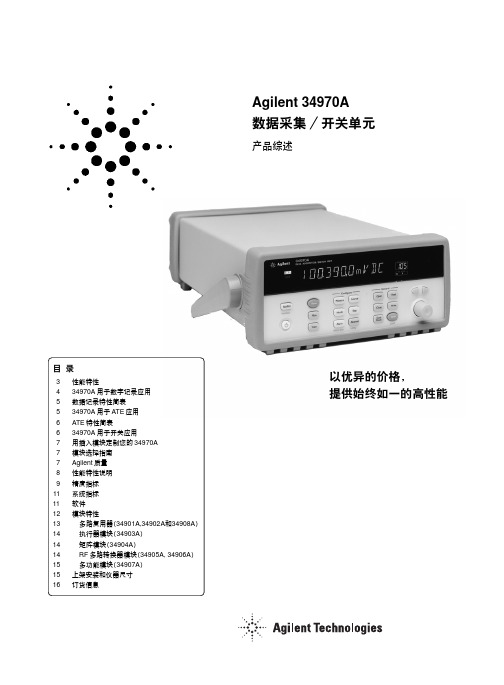
这是一台数据采集前端: 34970A 是具有优异测量性能的自动测试系统 提
供您所需要的精度、分辨率和速度。请见第 5 页上的应用 信息。
得心应手的更好测量
您不满于大多数其它数据记录仪或数据采集插卡的平 庸性能吗? 34970A 提供 61/2 位分辨率和 0.004% 的基本直 流电压年精度。
用 Agilent BenchLink Data Logger II 软件简 化您的数据收集和分析
可定制的配置 34970A 有 3 个模块插槽和 8 种开关 / 控制模块,您能
按要求定制该仪器。仅购买当前所需, 而日后随应用的增 加再添置更多的模块。
易用性 从简化的配置过程到自引导的前面板界面,我们为易
用性付出了大量时间和精力。包括模块上的螺钉终端连接 器,内置的热偶参考结,有大量应用实例和测试技巧的用 户文档,以及标准的仪器启用套件,您只需花 15 分钟就能 加装模块并开始测量,无论您是否经常使用仪器。
能力和性能: 0.004% 基本直流电压年精度,0.06%基本交 流电压年精度和 0.01% 基本电阻年精度。我们的专利多斜 III A-D 技术提供优异的线性度(2ppm 读数 + 1ppm 量程) 及 22bit分辨率。由于这是一种积分式 A/D,因此有非常高 的噪声抑制能力,能适应高噪声的 PC 插卡和采样 A/D 环 境。不需要平均多次采样,就能看到您所要的实际数据。 如果您需要高扫描率,34970A 能以高达250 通道/ 秒的速 度提供经完全转换的测量。
5
软件驱动程序 您不再需要为开发测试系统软件花几个月时间。
34970A 的软件驱动程序支持 Agilent VEE 和 NI LabView, 能容易地集成至您的测试系统。标准 RS-232 和 GPIB 接口 及 SCPI 程序语言使集成更为容易。
- 1、下载文档前请自行甄别文档内容的完整性,平台不提供额外的编辑、内容补充、找答案等附加服务。
- 2、"仅部分预览"的文档,不可在线预览部分如存在完整性等问题,可反馈申请退款(可完整预览的文档不适用该条件!)。
- 3、如文档侵犯您的权益,请联系客服反馈,我们会尽快为您处理(人工客服工作时间:9:00-18:30)。
LINEAR TECHNOLOGY LT3497 Manual /file/2545325From collects and classifies the global productinstrunction manuals to help users access anytime andanywhere, helping users make better use of products.Home: / Chinese: /3497fELECTRICAL CHARACTERISTICS PACKAGE/ORDER INFORMATIONABSOLUTE MAXIMUM RATINGSInput Voltage (VIN) ...................................................10V SW1, SW2 Voltages ..................................................35V CAP1, CAP2 Voltages ................................................35V CTRL1, CTRL2 Voltages ............................................10V LED1, LED2 Voltages ................................................35V Operating Temperature Range .................–40°C to 85°C Maximum Junction Temperature ..........................125°C Storage Temperature Range ...................–65°C to 125°C(Note 1)PARAMETERCONDITIONS MIN TYP MAX UNITSMinimum Operating Voltage2.5V LED Current Sense Voltage (V CAP1 – V LED1)V CAP1 = 16V ●190200210mV LED Current Sense Voltage (V CAP2 – V LED2)V CAP2 = 16V●190200210mV Offset Voltage (V OS ) Between(V CAP1 – V LED1) – (V CAP2 – V LED2) Voltages V OS = |(V CAP1 – V LED1) – (V CAP2 – V LED2)|028mV CAP1, LED1 Pin Bias Current V CAP1 = 16V, V LED1 = 16V 2040µA CAP2, LED2 Pin Bias CurrentV CAP2 = 16V, V LED2 = 16V2040µA V CAP1, V LED1 Common Mode Minimum Voltage 2.5V V CAP2, V LED2 Common Mode Minimum Voltage 2.5V Supply CurrentV CAP1 = V CAP2 = 16V, V LED1 = V LED2 = 15V, V CTRL1 = V CTRL2 = 3V 68.5mA V CTRL1 = V CTRL2 = 0V1218µA Switching Frequency 1.8 2.3 2.8MHz Maximum Duty Cycle8892%Converter 1 Switch Current Limit SW1●300400mA Converter 2 Switch Current Limit SW2●300400mA Converter 1 V CESAT I SW1 = 200mA 200mV Converter 2 V CESAT I SW2 = 200mA 200mVSwitch 1 Leakage Current V SW1 = 16V 0.1 5µA Switch 2 Leakage CurrentV SW2 = 16V0.15µATOP VIEW11DDB PACKAGE10-LEAD (3mm × 2mm) PLASTIC DFN LED1CTRL1GND CTRL2LED2CAP1SW1V IN SW2CAP268791054231T JMAX = 125°C, θJA = 76°C/W, θJC = 13.5°C/WEXPOSED PAD (PIN 11) IS GND, MUST BE SOLDERED TO PCBORDER PART NUMBERDDB PART MARKINGLT3497EDDBLCGTOrder Options Tape and Reel: Add #TRLead Free: Add #PBF Lead Free Tape and Reel: Add #TRPBF Lead Free Part Marking: /leadfree/Consult LTC Marketing for parts specifi ed with wider operating temperature ranges.The ● denotes the specifi cations which apply over the full operatingtemperature range, otherwise specifi cations are at T A = 25°C. V IN = 3V, V CTRL1 = V CTRL2 = 3V.3497fNote 1: Stresses beyond those listed under Absolute Maximum Ratings may cause permanent damage to the device. Exposure to any Absolute Maximum Rating condition for extended periods may affect device reliability and lifetime.PARAMETERCONDITIONS MIN TYP MAX UNITSV CTRL1 Voltage for Full LED Current V CAP1 = 16V ● 1.5V V CTRL2 Voltage for Full LED Current V CAP2 = 16V● 1.5V V CTRL1 or V CTRL2 Voltage to Turn On the IC ●100mVV CTRL1 and V CTRL2 Voltages to Shut Down the IC 50mV CTRL1, CTRL2 Pin Bias Current 100nA CAP1 Pin Overvoltage Protection ●303234V CAP2 Pin Overvoltage Protection ●303234V Schottky 1 Forward Drop I SCHOTTKY1 = 100mA 0.8V Schottky 2 Forward DropI SCHOTTKY2 = 100mA 0.8VSchottky 1 Reverse Leakage Current V R1 = 25V 4µA Schottky 2 Reverse Leakage CurrentV R2 = 25V4µAELECTRICAL CHARACTERISTICS The ● denotes the specifi cations which apply over the full operatingtemperature range, otherwise specifi cations are at T A = 25°C. V IN = 3V, V CTRL1 = V CTRL2 = 3V.Note 2: The LT3497E is guaranteed to meet performance specifi cations from 0°C to 85°C. Specifi cations over the –40°C to 85°C operatingtemperature range are assured by design, characterization and correlation with statistical process controls.200ms/DIV3497 G07 V IN = 3.6VFRONT PAGEAPPLICATION CIRCUIT1ms/DIV3497 G08 V IN = 3.6VFRONT PAGEAPPLICATION CIRCUIT3497fPIN FUNCTIONSLED1 (Pin 1): Connection point for the anode of the fi rst LED of the fi rst set of LEDs and the sense resistor (R SENSE1). The LED current can be programmed by: I mV R LED SENSE 11200=CTRL1 (Pin 2): Dimming and Shutdown Pin. Connect CTRL1 below 50mV to disable converter 1. As the pin volt-age is ramped from 0V to 1.5V, the LED current ramps from 0 to (I LED1 = 200mV/R SENSE1). The CTRL1 pin must not be left fl oating.GND (Pin 3): Connect the GND pin to the PCB system ground plane.CTRL2 (Pin 4): Dimming and Shutdown Pin. Connect CTRL2 below 50mV to disable converter 2. As the pin volt-age is ramped from 0V to 1.5V, the LED current ramps from 0 to (I LED2 = 200mV/R SENSE2). The CTRL2 pin must not be left fl oating.LED2 (Pin 5): Connection point for the anode of the fi rst LED of the second set of LEDs and the sense resistor (R SENSE2). The LED current can be programmed by: I mV R LED SENSE 22200=CAP2 (Pin 6): Output of Converter 2. This pin is connected to the cathode of internal Schottky diode 2. Connect the output capacitor to this pin and the sense resistor (R SENSE2) from this pin to LED2 pin.SW2 (Pin 7): Switch Pin. Minimize trace area at this pin to minimize EMI. Connect the inductor at this pin.V IN (Pin 8): Input Supply Pin. This pin must be locally bypassed.SW1 (Pin 9): Switch Pin. Minimize trace area at this pin to minimize EMI. Connect the inductor at this pin.CAP1 (Pin 10): Output of Converter 1. This pin is connected to the cathode of internal Schottky diode 1. Connect the output capacitor to this pin and the sense resistor (R SENSE1) from this pin to LED1 pin.Exposed Pad (Pin 11): Ground. Must be soldered to PCB.3497fOPERATIONMain Control LoopThe LT3497 uses a constant frequency, current mode con-trol scheme to provide excellent line and load regulation. It incorporates two identical, but fully independent PWM converters. Operation can be best understood by referring to the Block Diagram in Figure 1. The oscillator, start-up bias and the band gap reference are shared between the two converters. The control circuitry, power switch, Schottky diode etc., are identical for both the converters. At power up, the capacitors at CAP1 and CAP2 pins are charged up to V IN (input supply voltage) via their respective inductor and the internal Schottky diode. If either CTRL1 and CTRL2 or both are pulled higher than 100mV, the bandgap reference, the start-up bias and the oscillator are turned on.The main control loop can be understood by following the operation of converter 1. At the start of each oscillator cycle, the power switch, Q1, is turned on. A voltage proportional to the switch current is added to a stabilizing ramp and the resulting sum is fed into the positive terminal of the PWM comparator, A2. When this voltage exceeds the level at the negative input of A2, the PWM logic turns off the power switch. The level at the negative input of A2 is set by the error amplifi er, A1, and is simply an amplifi ed version of the difference between the V CAP1 and V LED1 voltage and the bandgap reference. In this manner the error amplifi er,A1, sets the correct peak current level in inductor L1 tokeep the output in regulation. The CTRL1 pin is used to adjust the LED current.If only one of the converters is turned on, the other converter will stay off and its output will remain charged up to V IN (input supply voltage). The LT3497 enters into shutdown when both CTRL1 and CTRL2 pins are pulled lower than 50mV. The CTRL1 and CTRL2 pins perform independent dimming and shutdown control for the two converters. Minimum Output CurrentThe LT3497 can drive a 4-LED string at 2mA LED current without pulse skipping. As current is further reduced, the device may begin skipping pulses.This will result in some low frequency ripple, although the average LED current remains regulated down to zero. The photo in Figure 2 details circuit operation driving 4 white LEDs at 2mA. Peak inductor current is less than 50mA and the regulator operates in discontinuous mode, meaning the inductor current reaches zero during the discharge phase. After the inductor current reaches zero, the SW pin exhibits ringing due to the LC tank circuit formed by the inductor in combination with the switch and the diode capacitance. This ringing is not harmful; far less spectral energy is contained in the ringing than in the switch transitions.Figure 2. Switching WaveformsI L50mA/DIVV SW 10V/DIVV IN = 4.2V I LED = 2mA 4 LEDs200ns/DIV3497 F02APPLICATIONS INFORMATION DUTY CYCLEThe duty cycle for a step-up converter is given by:DV V VV V VOUT D INOUT D CESAT =++––where:V OUT = Output voltageV D = Schottky forward voltage dropV CESAT = Saturation voltage of the switchV IN = Input voltageThe maximum duty cycle achievable for LT3497 is 88% when running at 2.3MHz switching frequency. Always ensure that the converter is not duty-cycle limited when powering the LEDs at a given frequency. INDUCTOR SELECTIONA 15µH inductor is recommended for most LT3497 ap-plications. Although small size and high effi ciency are major concerns, the inductor should have low core losses at 2.3MHz and low DCR (copper wire resistance). Some inductors in this category with small size are listed in Table 1. The effi ciency comparison of different inductors is shown in Figure 3.Table 1: Recommended InductorsPARTL(µH)MAXDCR(Ω)CURRENTRATING(mA)VENDORLQH32CN150K53 LQH2MCN150K02 LQH32CN100K53 LQH2MCN100K02151510100.581.60.31.2300200450225MurataSD3112-150150.654440Cooper1001AS-150M (TYPE D312C)150.80360TokoCDRH2D11/HP150.739410SumidaCAPACITOR SELECTIONThe small size of ceramic capacitors make them ideal for LT3497 applications. Use only X5R and X7R types because they retain their capacitance over wider temperature ranges than other types such as Y5V or Z5U. A 1µF input capacitor and a 1µF output capacitor are suffi cient for most applica-tions. Table 2 shows a list of several ceramic capacitor manufacturers. Consult the manufacturers for detailed information on their entire selection of ceramic parts. Table 2: Recommended Ceramic Capacitor ManufacturersTaiyo Yuden(800) 368-2496AVX(803) 448-9411Murata(714) 852-2001OVERVOLTAGE PROTECTIONThe LT3497 has an internal open-circuit protection circuit for both converters. In the cases of output open circuit, when the LEDs are disconnected from the circuit or the LEDs fail open circuit, the converter V CAP voltage is clamped at 32V (typ). Figure 4a shows the transient response of the front page application step-up converter with LED1 disconnected. With LED1 disconnected, the converter starts switching at the peak inductor current limit. The converter output starts ramping up and fi nally gets clamped at 32V (typ). The converter will then switch at low inductor current to regulate the converter output at the clamp voltage. The V CAP and input current during output open circuit are shown in the Typical Performance Characteristics.Figure 3. Effi ciency Comparison of Different InductorsLED CURRENT (mA)65708015µH MURATA LQH32CN150K5315µH MURATA LQH2MCN150K0215µH COOPER SD3112-15015µH TOKO 1001AS-150M TYPE D312C15µH SUMIDA CDRH2D11/HP153497 F03605551020504575EFFICIENCY(%)3497fFigure 4b. Switching Waveforms with Output 1 Open CircuitI SW200mA/DIVV CAP 10V/DIVV IN = 3.6V 4 LEDsLED 2 DISCONNECTED200ms/DIV3497 F04b2ms/DIV3497 F07 V IN = 3.6V4 LEDsFigure 7. Direct PWM Dimming WaveformsInformation furnished by Linear Technology Corporation is believed to be accurate and reliable. However, no responsibility is assumed for its use. Linear Technology Corporation makes no representa-tion that the interconnection of its circuits as described herein will not infringe on existing patent rights.。
