UMT1C4R7MDD中文资料
mcp4017中文规格书

mcp4017中文规格书MCP4017中文规格书MCP4017是一款CMOS数字电位器,由Microchip公司推出。
它是一种单通道、6位数的电位器,采用了串行控制接口。
MCP4017能够提供多种电阻调节功能,适用于各种电路和系统。
MCP4017的主要特点包括:1. 6位数字电阻调节范围:MCP4017可以提供64个不同的电阻值,范围从0Ω到50kΩ,可根据需要进行调节。
2. 串行控制接口:MCP4017通过串行接口进行控制,使用简单方便。
用户可以通过外部控制器向MCP4017发送指令,实现电阻值的调整。
3. 低功耗:MCP4017具有低功耗特性,适用于对功耗要求较高的应用。
在待机模式下,MCP4017的功耗非常低,可帮助延长电池寿命。
4. 高精度:MCP4017具有较高的电阻调节精度,可以满足精确控制要求。
其调节精度可达到0.1%。
5. 温度稳定性:MCP4017具有良好的温度稳定性,能够在广泛的温度范围内提供稳定的电阻值。
这使得它在各种环境条件下都能够可靠地工作。
6. 多种封装形式:MCP4017提供了多种封装形式,包括SOIC、MSOP 和DFN等,以满足不同应用的需求。
MCP4017的主要应用领域包括模拟电路的增益调节、电压和电流的控制、电源管理等。
例如,在音频放大器中,MCP4017可以用于调节放大器的增益,实现音量控制功能。
在电源管理系统中,MCP4017可以用于调节电源输出的电流或电压,以满足不同设备的需求。
MCP4017的工作原理是通过调节内部电阻网络的连接方式,实现电阻值的调整。
用户可以通过串行接口发送指令给MCP4017,控制电阻网络的连接方式,从而改变电阻值。
MCP4017内部有一个电阻网络选择器,通过选择不同的电阻网络,可以得到不同的电阻值。
这种电阻调节方式具有快速、精确、可靠的特点。
MCP4017是一款功能强大、性能稳定的CMOS数字电位器。
它的特点包括6位数字调节范围、低功耗、高精度、温度稳定性和多种封装形式。
产品推介ppt_产品推介

产品推介ppt_产品推介源科全球首款单芯片SATA DOM固态硬盘小源面市国内固态存储领域的领导者源科公司宣布推出全球首款单芯片SATA DOM固态硬盘“小源”,它是rSSD系列新增的一员“小”将。
小源SATA DOM固态硬盘是基于源科自主研发的芯片级rSSD,该产品采用了SATA II接口,相比曾经市场主流的IDE/ ATA DOM盘,其性能和可靠性更加稳定。
采用rSSD作为存储介质的“小源”同样具有小尺寸、高性能的优点,同时,该产品具备的写保护功能使其可靠性更强。
值得一提的是,源科小源SATA DOM 硬盘标准版配备5V外接电源,也可为进一步节省空间选配7引脚VCC电源。
风河推出Android车载信息娱乐系统快速开发软件工具风河公司近日推出汽车市场专用软件,进一步扩大其Android产品组合,Wind River Solution Accelerator for Android - Automotive主要功能包括:连接iPod/iPhone/iPad以提供丰富的多媒体功能、消费者可修改的定制用户接口以及FM收音机功能,此外,风河还提供软件和系统集成方面的专业服务,为不同的客户项目提供支持。
此开发工具能够帮助车载信息娱乐设备制造商缩短基于Android平台系统的开发时间。
华北工控“CedarTrail”智能应用平台满足不同需求自英特尔新一代凌动“CedarTrail”平台上市后,华北工控就发布了2款Mini ITX主板,公司根据市场反馈又研发了多款针对不同应用领域的新的“CedarTrail”智能应用平台,包括满足安防数字视频监控、SOHO型的存储服务以及工业现场自动化控制需求的BPC-7932、应用于数字标牌、汽车车载娱乐、多媒体设备、零售等智能终端的BIS-6555和适合轨道交通、智能医疗设备以工业自动化领域应用的EMB-3930等。
ST量产STM32 F0入门级MCU意法半导体(ST)开始量产STM32 F0系列32位微控制器。
CMD5D13NP-4R7M中文资料
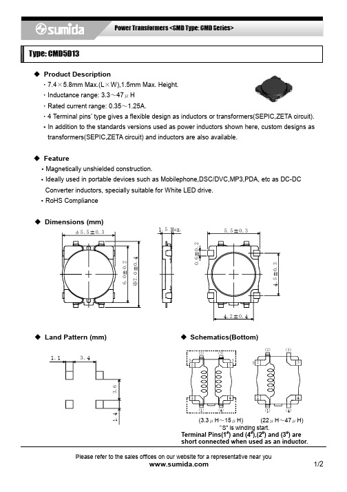
(3.3μH~15μH) (22μH~47μH) “S" is winding start.
1/2
元器件交易网
Power Transformers <SMD Type: CMD Series>
Type: CMD5D13
◆ Specification
◆ Dimensions (mm)
φ5.5±0.3 1.5 Max.
0.6±0.2
5.5±0.3
※7.0 ±0.4
6.0 ±0.2
4.2±0.4
◆ Land Pattern (mm)
1.1 3.4
◆ Schematics(Bottom)
(2) S 2 3 (3) S
(2) S 2
ቤተ መጻሕፍቲ ባይዱ
4.5 ±0.3
(3) 3 1 (1) (4)
3.6
1 (1) (4)
4
4
1.4
Terminal Pins(1#) and (4#),(2#) and (3#) are short connected when used as an inductor.
Please refer to the sales offices on our website for a representative near you
Part No. ※ CMD5D13NP-3R3M□ CMD5D13NP-4R7M□ CMD5D13NP-6R8M□ CMD5D13NP-100M□ CMD5D13NP-150M□ CMD5D13NP-220M□ CMD5D13NP-330M□ CMD5D13NP-470M□ Stamp 3R3 4R7 6R8 100 150 220 330 470 Inductance (μH) [Within] 100kHz/1V 3.3±20% 4.7±20% 6.8±20% 10±20% 15±20% 22±20% 33±20% 47±20% D.C.R.(mΩ) Max.(Typ.) (at 20℃) 81 (65) 106 (85) 144 (115) 187 (150) 300 (240) 431 (345) 637 (510) 875 (700) Saturation Current(A) (at 20℃)※1 1.90 1.50 1.40 1.00 0.95 0.80 0.70 0.55 Temperature Rise current (A) ※2 1.25 1.20 0.90 0.85 0.57 0.54 0.38 0.35
莫莎公司 OnCell G2111 G2151I 系列工业四频GSM GPRS模块产品简介说明书

OnCell G2111/G2151I SeriesIndustrial quad-band GSM/GPRS modemsFeatures and Benefits•Quad-band GSM/GPRS850/900/1800/1900MHz•DIN-rail mounting and wall mounting•2.5kV RMS isolation for1min.for all serial signals(G2151I only)•LED indicators for GSM/GPRS and data transmission status•Extended operating temperature from-25to70°C(G2111-T only)CertificationsIntroductionThe OnCell G2111/G2151I Series of industrial quad-band GSM/GPRS modems are designed to transmit data and short messages(SMS)over GSM/ GPRS mobile networks.The modems can be used to increase the efficiency of maintenance and communication,but do not require extensive training.In addition,the modems can be mounted on a DIN rail or wall.The OnCell G2111/G2151I Series modems accept a12to48VDC power input,making them suitable for use with a variety of field power sources.The serial ports feature15kV ESD line protection to protect the products from harmful electrical discharge,and separate RS-232and RS-422/485 interfaces are built into the OnCell G2151I,each with2.5kV RMS isolation protection for one minute.The two serial interfaces on the OnCell G2151I make it ideal for attaching all kinds of devices,such as stand-alone controllers,PC COM ports,and multi-dropped electric meters.In addition,the OnCell G2111-T has an extended operating temperature(-25to70°C)design that makes it suitable for heavy industrial use. SpecificationsCellular InterfaceCellular Standards GSM,GPRSBand Options Quad-band GSM/GPRS850MHz/900MHz/1800MHz/1900MHzGPRS Multi-Slot Class10GPRS Terminal Device Class Class BGPRS Coding Schemes CS1to CS4CSD Data Rates Up to14400bpsCellular Antenna Connectors1SMA femaleNo.of SIMs1SIM Control Voltage3VSerial InterfaceNo.of Ports1Serial Standards All models:RS-232(DB9female connector)OnCell G2151I:RS-232/422/485(5-pin terminal block connector)ESD Protection OnCell G2111:15kVIsolation OnCell G2151I:2kVData Bits8Stop Bits1Parity NoneFlow Control RTS/CTSBaudrate300bps to230.4kbpsSerial SignalsRS-232TxD,RxD,RTS,CTS,DTR,DSR,DCD,RI,GNDRS-422Tx+,Tx-,Rx+,Rx-,GNDRS-485-2w Data+,Data-,GNDRS-485-4w Tx+,Tx-,Rx+,Rx-,GNDPower ParametersInput Voltage12to48VDCPower Connector Terminal blockInput Current0.625A@12VDC,0.16A@48VDCPhysical CharacteristicsHousing ABS+PolycarbonateIP Rating IP30Dimensions27x123x79mm(1.06x4.84x3.11in)Weight155g(0.34lb)Environmental LimitsOperating Temperature OnCell G2111/G2151I:-20to55°C(-4to131°F)OnCell G2111I-T:-25to70°C(-22to158°F)Storage Temperature(package included)-40to75°C(-40to167°F)Ambient Relative Humidity5to95%(non-condensing)Standards and CertificationsSafety UL60950-1EMC EN55032/24EMI CISPR32,FCC Part15B Class AEMS IEC61000-4-2ESD:Contact:4kV;Air:8kVIEC61000-4-3RS:80MHz to1GHz:3V/mIEC61000-4-4EFT:Power:0.5kVIEC61000-4-5Surge:Power:1kVIEC61000-4-6CS:3VIEC61000-4-8PFMFRadio Frequency FCC Part22H,FCC Part24E,EN301489-1,EN301489-7,EN301511MTBFTime OnCell G2111:925,000hrsOnCell G2111-T:925,000hrsOnCell G2151I:864,000hrsStandards Telcordia SR332WarrantyWarranty Period5yearsDetails See /warrantyPackage ContentsDevice1x OnCell G2111/G2151I Series GSM/GPRS modem1Antenna1x GSM/GPRSAccessory1x terminal block for power jack connectorDocumentation1x quick installation guide1x warranty cardDimensionsOrdering InformationModel Name Cellular Standard Band Operating Temp.Serial Isolation Serial StandardsOnCell G2111GSM/GPRS 850/900/1800/1900MHz-20to55°C–RS-232OnCell G2111-T GSM/GPRS 850/900/1800/1900MHz-25to70°C–RS-232OnCell G2151I GSM/GPRS 850/900/1800/1900MHz-20to55°C✓RS-232/422/4851.An activated SIM card(not included)must be provided by a third party Cellular Service Provider.Accessories(sold separately)AntennasANT-CQB-AHSM-00-3m GSM/GPRS/EDGE,omni-directional magnetic base antenna,0dBi,3m cableANT-CQB-AHSM-03-3m GSM/GPRS/EDGE,omni-directional magnetic base antenna,3dBi,3m cableANT-CQB-AHSM-05-3m GSM/GPRS/EDGE,omni-directional magnetic base antenna,5dBi,3m cableANT-CQB-ASM-01GSM/GPRS/EDGE,omni-directional rubber duck antenna,1dBiANT-WCDMA-ANF-00GSM/GPRS/EDGE/UMTS/HSPA,omni-directional outdoor antenna,0dBiANT-WCDMA-ASM-1.5GSM/GPRS/EDGE/UMTS/HSPA,omni-directional rubber duck antenna,1.5dBiANT-WCDMA-AHSM-04-2.5m GSM/GPRS/EDGE/UMTS/HSPA,omni-directional magnetic base antenna,4dBiANT-LTE-ASM-02GPRS/EDGE/UMTS/HSPA/LTE,omni-directional rubber duck antenna,2dBiANT-LTE-ANF-04GSM/GPRS/EDGE/UMTS/HSPA/LTE,omni-directional outdoor antenna,4dBi,IP66AntennasANT-LTEUS-ASM-01GSM/GPRS/EDGE/UMTS/HSPA/LTE,omni-directional rubber duck antenna,1dBiWireless Antenna CableA-CRF-SMSF-R3-100Cellular magnetic-base SMA connector with1-meter RF cable©Moxa Inc.All rights reserved.Updated Nov12,2018.This document and any portion thereof may not be reproduced or used in any manner whatsoever without the express written permission of Moxa Inc.Product specifications subject to change without notice.Visit our website for the most up-to-date product information.。
UMTS基础

软切换流程示意图
CN RNC
Node B
AirBridge
AirBridge
AirBridge
软切换流程示意图
RNC CN
Node B
AirBridge
AirBridge
AirBridge
同频 – 不同码
⇒ Rake 接受/分集合并
软切换流程示意图
RNC CN
Node B
AirBridge
AirBridge
Serving RNC
Node B
AirBridge AirBridge
AirBridge
硬切换流程示意图(RNC内)
CN
SRNC
CN
SRNC
NodeB
NodeB
NodeB
NodeB
硬切换前
硬切换后
无线链路不能够同时保存
硬切换流程示意图(跨RNC)
CN
SRNC
CN
SRNC
RNC
RNC
NodeB
NodeB
AirBridge
同频 – 不同码
⇒RNC分集合并
软切换流程示意图(SRNC-DRNC)
Serving RNC
CN
Drift RNC
Node B
AirBridge AirBridge
AirBridge
同频 – 不同码
⇒SRNC分集合并, ⇒DRNC透传
软切换流程示意图(SRNS迁移)
RNC CN
Source RNC与Target RNC
切换相关概念
激活集:UE与UTRAN之间为同一通信业务服务 的无线链路集。 软切换:软切换就是一个往激活集中增加和/ 或删 除无线链路的过程,包括无线链路增加, 无线链 路删除和无线链路替换,无线链路替换就是同时 增加和删除无线链路(在活动集达到最大容量 时)。 更软切换:发生在一个小区内不同扇区间的软切 换,RNC不参与。 硬切换:切换过程中先中断与原小区间的通信, 例如异频切换。
1UMTS概述

24
> UMTS:Universal Mobile Telecommunications System
• • • “通用移动通信系统” 欧洲电信标准化协会(ETSI)所积极推进的第三代移动通信系统 W-CDMA 将用于广域范围内的移动通信
•
TD-CDMA 将主要用于低移动性室内通信
8
UMTS简介 UMTS FDD/TDD
• 全球范围高度的兼容性
– – 1885MHz~2025MHz,2110MHz~2200MHz 1980MHz~2010MHz,2170MHz~2200MHz(卫星移动通信系统) A 快速移动环境,最高速率 144kbit/s B 步行环境下,最高速率 384kbit/s C 室内环境,最高速率 2Mbit/s
GSM 用户是以频率( FDMA )和 时间 ( TDMA )区分的
UMTS 用户以地址码( CDMA )区分
12
UMTS简介 练习
哪个是 UMTS 中 CDMA 的载波带宽?
1/ 200 kHz 2/ 1 MHz 3/ 5 MHz
关于 UMTS 复用模式,哪些说法是正确的?
1/ FDD 类似于 GSM 的 双工模式 2/ TDD 和 FDD 使用相同的频率 3/ FDD 更适合非对称业务 4/ TDD 不支持对称业务
UMTS概述
从2G到3G 第三代移动通信系统
> IMT2000 (International Mobile Telecommunications-2000)
• • 1985年ITU(国际电联)提出FPLMTS(未来公众陆地移动通信系统) 1996年正式更名为IMT2000
> IMT-2000系统无线接口的基本要求
微尔赛米集团2013年产品说明书
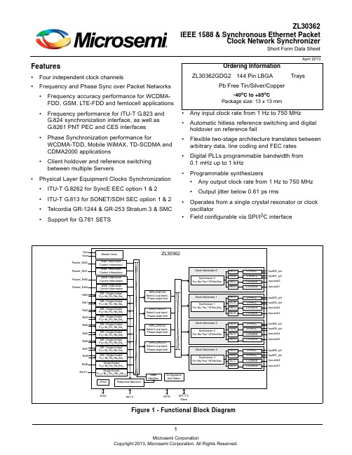
1Features•Four independent clock channels•Frequency and Phase Sync over Packet Networks •Frequency accuracy performance for WCDMA-FDD, GSM, LTE-FDD and femtocell applications •Frequency performance for ITU-T G.823 and G.824 synchronization interface, as well as G.8261 PNT PEC and CES interfaces•Phase Synchronization performance forWCDMA-TDD, Mobile WiMAX, TD-SCDMA and CDMA2000 applications•Client holdover and reference switching between multiple Servers•Physical Layer Equipment Clocks Synchronization •ITU-T G.8262 for SyncE EEC option 1 & 2•ITU-T G.813 for SONET/SDH SEC option 1 & 2•Telcordia GR-1244 & GR-253 Stratum 3 & SMC •Support for G.781 SETS•Any input clock rate from 1Hz to 750MHz •Automatic hitless reference switching and digital holdover on reference fail•Flexible two-stage architecture translates between arbitrary data, line coding and FEC rates •Digital PLLs programmable bandwidth from 0.1mHz up to 1kHz•Programmable synthesizers•Any output clock rate from 1 Hz to 750 MHz •Output jitter below 0.61 ps rms•Operates from a single crystal resonator or clock oscillator•Field configurable via SPI/I 2C interfaceApril 2013Figure 1 - Functional Block DiagramZL30362IEEE 1588 & Synchronous Ethernet PacketClock Network SynchronizerShort Form Data SheetOrdering InformationZL30362GDG2144 Pin LBGATraysPb Free Tin/Silver/Copper-40o C to +85o CPackage size: 13 x 13 mmDetailed FeaturesGeneral•Four independent clock channels•Operates from a single crystal resonator or clock oscillator•Configurable its SPI/I2C interfaceTime Synchronization Algorithm•External algorithm controls software digital PLL to adjust frequency & phase alignment•Frequency, Phase and Time Synchronization over IP, MPLS and Ethernet Packet Networks•Frequency accuracy performance for WCDMA-FDD, GSM, LTE-FDD and femtocell applications, with target performance less than ± 15 ppb.•Frequency performance for ITU-T G.823 and G.824 synchronization interface, as well as G.8261 PNT EEC, PNT PEC and CES interface specifications.•Phase Synchronization performance for WCDMA-TDD, Mobile WiMAX, TD-SCDMA and CDMA2000 applications with target performance less than ± 1 s phase alignment.•Time Synchronization for UTC-traceability and GPS replacement.•Client reference switching between multiple Servers•Client holdover when Server packet connectivity is lostElectrical Clock Inputs•Nine input references configurable as single ended or differential and two single ended input references •Synchronize to any clock rate from 1 Hz to 750 MHz on differential inputs•Synchronize to any clock rate from 1 Hz to 177.75 MHz on singled-ended inputs•Any input reference can be fed with sync (frame pulse) or clock.•Synchronize to sync pulse and sync pulse/clock pair.•Flexible input reference monitoring automatically disqualifies references based on frequency and phase irregularities•LOS•Single cycle monitor•Precise frequency monitor•Coarse frequency monitor•Guard soak timer•Per input clock delay compensationElectrical Clock Engine•Digital PLLs filter jitter from 0.1 mHz up to 1 kHz•Flexible two-stage architecture translates between arbitrary data rates, line coding rates and FEC rates •Internal state machine automatically controls mode of operation (free-run, locked, holdover)•Automatic hitless reference switching and digital holdover on reference fail•Physical-to-physical reference switching•Physical-to-packet reference switching•Packet-to-physical reference switching•Packet-to-packet reference switching•Support for wide variety of Equipment Clock specifications•SyncE•ITU-T G.8262 option 1 EEC (Europe/China)•ITU-T G.8262 option 2 (USA)•SONET/SDH•ITU-T G.813 option 1 SEC (Europe/China)•ITU-T G.813 option 2 (USA)•ANSI T1.105/Telcordia GR-253 Stratum 3 for SONET•Telcordia GR-253 SMC•PDH•ITU-T G.812 Type I SSU•ITU-T G.812 Type III, ANSI T1.101/Telcordia GR-1244 Stratum 3E, including phase build out•ANSI T1.101/Telcordia GR-1244 Stratum 3•ANSI T1.101/Telcordia GR-1244 Stratum 4E/4•Selectable phase slope limiting•Holdover better than 1 ppb (when using < 0.1 Hz filter)•Supports ITU-T G.823, G.824 and G.8261 for 2048kbit/s and 1544kbit/s interfaces•Supports G.781 SETSElectrical Clock Generation•Four programmable synthesizers•Eight LVPECL outputs•Two LVPECL outputs per synthesizer•Generate any clock rate from 1 Hz to 750 MHz•Maximum jitter below 0.61 ps RMS•Meets OC-192, STM-64, 1 GbE & 10 GbE interface jitter requirements•Eight LVCMOS outputs•Two LVCMOS outputs per synthesizer•Generate any clock rate from 1 Hz to 177.75 MHz•Maximum jitter below 1 ps rms•Programmable output advancement/delay to accommodate trace delays or compensate for system routing paths•Outputs may be disabled to save powerAPI Software•Interfaces to 1588-capable PHY and switches with integrated timestamping•Abstraction layer for independence from OS and CPU, from embedded SoC to home-grown•Fits into centralized, highly integrated pizza box architectures as well as distributed architectures with multiple line cards and timing cardsApplications•ITU-T G.8262 System Timing Cards which support 1GbE and 10GbE interfaces•Telcordia GR-253 Carrier Grade SONET/SDH Stratum 3 System Timing Cards•System Timing Cards which supports ITU-T G.781 SETS (SDH Equipment Timing Source)•Integrated basestation reference clock for air interface for GSM, WCDMA, LTE and WiMAX macro, micro or femtocells•Mobile Backhaul NID, edge router or access aggregation node•EPON/GE-PON & GPON OLT•EPON/GE-PON & GPON ONU/OLT•DSLAM and RT-DSLAM•10Gigabit line cards•Synchronous Ethernet, 10GBASE-R and 10GBASE-W•SONET/SDH, Fibre Channel, XAUIInformation relating to products and services furnished herein by Microsemi Corporation or its subsidiaries (collectively “Microsemi”) is believed to be reliable. However, Microsemi assumes no liability for errors that may appear in this publication, or for liability otherwise arising from the application or use of any suchinformation, product or service or for any infringement of patents or other intellectual property rights owned by third parties which may result from such application or use. Neither the supply of such information or purchase of product or service conveys any license, either express or implied, under patents or other intellectual property rights owned by Microsemi or licensed from third parties by Microsemi, whatsoever. Purchasers of products are also hereby notified that the use of product in certain ways or in combination with Microsemi, or non-Microsemi furnished goods or services may infringe patents or other intellectual property rights owned by Microsemi.This publication is issued to provide information only and (unless agreed by Microsemi in writing) may not be used, applied or reproduced for any purpose nor form part of any order or contract nor to be regarded as a representation relating to the products or services concerned. The products, their specifications, services and other information appearing in this publication are subject to change by Microsemi without notice. No warranty or guarantee express or implied is made regarding the capability, performance or suitability of any product or service. Information concerning possible methods of use is provided as a guide only and does not constitute any guarantee that such methods of use will be satisfactory in a specific piece of equipment. It is the user’s responsibility to fully determine the performance and suitability of any equipment using such information and to ensure that any publication or data used is up to date and has not been superseded.Manufacturing does not necessarily include testing of all functions or parameters. These products are not suitable for use in any medical and other products whose failure to perform may result in significant injury or death to the user. All products and materials are sold and services provided subject to Microsemi’s conditions of sale which are available on request.Purchase of Microsemi’s I 2C components conveys a license under the Philips I 2C Patent rights to use these components in an I 2C System, provided that the system conforms to the I 2C Standard Specification as defined by Philips.Microsemi, ZL, and combinations thereof, VoiceEdge, VoicePort, SLAC, ISLIC, ISLAC and VoicePath are trademarks of Microsemi Corporation.TECHNICAL DOCUMENTATION - NOT FOR RESALEFor more information about all Microsemi productsvisit our Web Site at/timing-and-synchronization。
MMSZ4xxxT1G系列和SZMMSZ4xxxT1G系列零点电阻电源器件的商品说明书

MMSZ4686T1G MMSZ4686T1G.MMSZ4xxxT1G Series, SZMMSZ4xxxT1G Series Zener Voltage Regulators 500 mW, Low I ZT SOD−123 Surface MountThree complete series of Zener diodes are offered in the convenient, surface mount plastic SOD−123 package. These devices provide a convenient alternative to the leadless 34−package style.Features•500 mW Rating on FR−4 or FR−5 Board•Wide Zener Reverse V oltage Range − 1.8 V to 43 V•Low Reverse Current (I ZT) − 50 m A•Package Designed for Optimal Automated Board Assembly •Small Package Size for High Density Applications•ESD Rating of Class 3 (>16 kV) per Human Body Model•SZ Prefix for Automotive and Other Applications Requiring Unique Site and Control Change Requirements; AEC−Q101 Qualified and PPAP Capable•These Devices are Pb−Free and are RoHS Compliant*Mechanical Characteristics:CASE:V oid-free, transfer-molded, thermosetting plastic case FINISH:Corrosion resistant finish, easily solderableMAXIMUM CASE TEMPERATURE FOR SOLDERING PURPOSES: 260°C for 10 SecondsPOLARITY:Cathode indicated by polarity band FLAMMABILITY RATING:UL 94 V−0MAXIMUM RATINGSRating Symbol Max Units Total Power Dissipation on FR−5 Board,(Note 1) @ T L = 75°CDerated above 75°C P D5006.7mWmW/°CThermal Resistance, (Note 2) Junction−to−Ambient R q JA340°C/WThermal Resistance, (Note 2) Junction−to−Lead R q JL150°C/WJunction and Storage Temperature Range T J, T stg−55 to+150°CStresses exceeding those listed in the Maximum Ratings table may damage the device. If any of these limits are exceeded, device functionality should not be assumed, damage may occur and reliability may be affected.1.FR−5 = 3.5 X 1.5 inches, using the minimum recommended footprint.2.Thermal Resistance measurement obtained via infrared Scan Method.*For additional information on our Pb−Free strategy and soldering details, please download the ON Semiconductor Soldering and Mounting Techniques Reference Manual, SOLDERRM/D.Cathode AnodeSee specific marking information in the device marking column of the Electrical Characteristics table on page 3 of this data sheet.DEVICE MARKING INFORMATIONSOD−123CASE 425STYLE 1Device Package Shipping†ORDERING INFORMATIONMARKING DIAGRAM†For information on tape and reel specifications, including part orientation and tape sizes, please refer to our T ape and Reel Packaging Specifications Brochure, BRD8011/D.MMSZ4xxxT1G SOD−123(Pb−Free)3,000 /Tape & ReelMMSZ4xxxT3G SOD−123(Pb−Free)10,000 /Tape & Reel xx= Device Code (Refer to page 3)M= Date CodeG= Pb−Free Package(Note: Microdot may be in either location)1SZMMSZ4xxxT1G SOD−123(Pb−Free)3,000 /Tape & ReelSZMMSZ4xxxT3G SOD−123(Pb−Free)10,000 /Tape & ReelELECTRICAL CHARACTERISTICS (T A = 25°C unless otherwise noted, V F = 0.9 V Max. @ I F = 10 mA)Symbol ParameterV Z Reverse Zener Voltage @ I ZTI ZT Reverse CurrentI R Reverse Leakage Current @ V RVR Reverse VoltageI F Forward CurrentV F Forward Voltage @ I FProduct parametric performance is indicated in the Electrical Characteristics for the listed test conditions, unless otherwise noted. Product performance may not be indicated by the Electrical Characteristics if operated under different conditions.ELECTRICAL CHARACTERISTICS (T A = 25°C unless otherwise noted, V F = 0.9 V Max. @ I F = 10 mA)Device*DeviceMarkingZener Voltage (Note 3)Leakage CurrentV Z (Volts)@ I ZT I R @ V RMin Nom Max m A m A VoltsMMSZ4678T1G CC 1.71 1.8 1.89507.51 MMSZ4679T1G CD 1.90 2.0 2.105051 MMSZ4680T1G CE 2.09 2.2 2.315041 MMSZ4681T1G CF 2.28 2.4 2.525021 MMSZ4682T1G CH 2.565 2.7 2.8355011 MMSZ4683T1G CJ 2.85 3.0 3.15500.81 MMSZ4684T1G CK 3.13 3.3 3.47507.5 1.5 MMSZ4685T1G CM 3.42 3.6 3.78507.52 MMSZ4686T1G CN 3.70 3.9 4.105052 MMSZ4687T1G CP 4.09 4.3 4.525042 SZMMSZ4687T1G CG6 4.09 4.3 4.525042 MMSZ4688T1G CT 4.47 4.7 4.9450103 MMSZ4689T1G CU 4.85 5.1 5.3650103 MMSZ4690T1G/T3G CV 5.32 5.6 5.8850104 MMSZ4691T1G CA 5.89 6.2 6.5150105 MMSZ4692T1G CX 6.46 6.87.145010 5.1 MMSZ4693T1G CY7.137.57.885010 5.7 MMSZ4694T1G CZ7.798.28.61501 6.2 MMSZ4695T1G DC8.278.79.14501 6.6 MMSZ4696T1G DD8.659.19.56501 6.9 MMSZ4697T1G DE9.501010.505017.6 MMSZ4698T1G DF10.451111.55500.058.4 MMSZ4699T1G DH11.401212.60500.059.1 MMSZ4700T1G DJ12.351313.65500.059.8 MMSZ4701T1G DK13.301414.70500.0510.6 MMSZ4702T1G DM14.251515.75500.0511.4 MMSZ4703T1G†DN15.201616.80500.0512.1 MMSZ4704T1G DP16.151717.85500.0512.9 MMSZ4705T1G DT17.101818.90500.0513.6 MMSZ4706T1G DU18.051919.95500.0514.4 MMSZ4707T1G DV19.002021.00500.0115.2 MMSZ4708T1G DA20.902223.10500.0116.7 MMSZ4709T1G DX22.802425.20500.0118.2 MMSZ4710T1G DY23.752526.25500.0119.0 MMSZ4711T1G†EA25.652728.35500.0120.4 MMSZ4712T1G EC26.602829.40500.0121.2 MMSZ4713T1G ED28.503031.50500.0122.8 MMSZ4714T1G EE31.353334.65500.0125.0 MMSZ4715T1G EF34.203637.80500.0127.3 MMSZ4716T1G EH37.053940.95500.0129.6 MMSZ4717T1G EJ40.854345.15500.0132.6 3.Nominal Zener voltage is measured with the device junction in thermal equilibrium at T L = 30°C ±1°C.*Include SZ-prefix devices where applicable.†MMSZ4703 and MMSZ4711 Not Available in 10,000/Tape & ReelTYPICAL CHARACTERISTICSV Z , T E M P E R A T U R E C O E F F I C I E N T (m V /C )°θV Z , NOMINAL ZENER VOLTAGE (V)Figure 1. Temperature Coefficients (Temperature Range −55°C to +150°C)V Z , T E M P E R A T U R E C O E F F I C I E N T (m V /C )°θ100101V Z , NOMINAL ZENER VOLTAGE (V)Figure 2. Temperature Coefficients (Temperature Range −55°C to +150°C)1.21.00.80.60.40.20T, TEMPERATURE (5C)Figure 3. Steady State Power Derating P p k, P E A K S U R G E P O W E R (W A T T S )PW, PULSE WIDTH (ms)Figure 4. Maximum Nonrepetitive Surge PowerP D , P O W E R D I S S I P A T I O N (W A T T S )V Z , NOMINAL ZENER VOLTAGEFigure 5. Effect of Zener Voltage onZener ImpedanceZ Z T , D Y N A M I C I M P E D A N C E ()ΩTYPICAL CHARACTERISTICSC , C A P A C I T A N C E (p F )V Z , NOMINAL ZENER VOLTAGE (V)Figure 6. Typical Capacitance 1000100101V Z , ZENER VOLTAGE (V)1001010.10.01I Z , Z EN E R C U R R E N T (m A )V Z , ZENER VOLTAGE (V)1001010.10.01I R , L E A K A G E C U R R E N T (A )μV Z , NOMINAL ZENER VOLTAGE (V)Figure 7. Typical Leakage Current10001001010.10.010.0010.00010.00001I Z , Z E N E R C U R R E N T (m A )Figure 8. Zener Voltage versus Zener Current(V Z Up to 12 V)Figure 9. Zener Voltage versus Zener Current(12 V to 91 V)SOD−123CASE 425−04ISSUE GDATE 07 OCT 2009SCALE 5:1NOTES:1.DIMENSIONING AND TOLERANCING PER ANSIY14.5M, 1982.2.CONTROLLING DIMENSION: INCH.DIM MIN NOM MAXMILLIMETERSINCHESA0.94 1.17 1.350.037A10.000.050.100.000b0.510.610.710.020c1.600.150.055D 1.40 1.80E 2.54 2.69 2.840.100---3.680.140L0.253.860.0100.0460.0020.0240.0630.1060.1450.0530.0040.0280.0710.1120.152MIN NOM MAX3.56H E---------0.006------------GENERICMARKING DIAGRAM**For additional information on our Pb−Free strategy and solderingdetails, please download the ON Semiconductor Soldering andMounting Techniques Reference Manual, SOLDERRM/D.SOLDERING FOOTPRINT**This information is generic. Please refer to device datasheet for actual part marking. Pb−Free indicator, “G” ormicrodot “ G”, may or may not be present.XXX= Specific Device CodeM= Date CodeG= Pb−Free Package1STYLE 1:PIN 1. CATHODE2. ANODE0.910.036ǒmminchesǓSCALE 10:1------q001010°°°°(Note: Microdot may be in either location) MECHANICAL CASE OUTLINEPACKAGE DIMENSIONSON Semiconductor and are trademarks of Semiconductor Components Industries, LLC dba ON Semiconductor or its subsidiaries in the United States and/or other countries.ON Semiconductor reserves the right to make changes without further notice to any products herein. ON Semiconductor makes no warranty, representation or guarantee regarding the suitability of its products for any particular purpose, nor does ON Semiconductor assume any liability arising out of the application or use of any product or circuit, and specifically disclaims any and all liability, including without limitation special, consequential or incidental damages. ON Semiconductor does not convey any license under its patent rights nor theON Semiconductor and are trademarks of Semiconductor Components Industries, LLC dba ON Semiconductor or its subsidiaries in the United States and/or other countries.ON Semiconductor owns the rights to a number of patents, trademarks, copyrights, trade secrets, and other intellectual property. A listing of ON Semiconductor’s product/patent coverage may be accessed at ON Semiconductor makes no warranty, representation or guarantee regarding the suitability of its products for any particular purpose, nor does ON Semiconductor assume any liability arising out of the application or use of any product or circuit, and specifically disclaims any and all liability, including without limitation special, consequential or incidental damages.PUBLICATION ORDERING INFORMATIONTECHNICAL SUPPORTNorth American Technical Support:Voice Mail: 1 800−282−9855 Toll Free USA/Canada Phone: 011 421 33 790 2910LITERATURE FULFILLMENT :Email Requests to:*******************ON Semiconductor Website: Europe, Middle East and Africa Technical Support:Phone: 00421 33 790 2910For additional information, please contact your local Sales RepresentativeMMSZ4686T1G MMSZ4686T1G.。
诺瓦科技无线LED控制卡T1-4G规格书
诺瓦科技无线LED控制卡T1-4G 规格书Taurus 系列多媒体播放器T1-4G 规格书文档版本:V1.3.2文档编号:NS120000336目录目录 .....................................................................................................................................................ii 1 概述 (1)1.1产品简介 ......................................................................................................................................................11.2应用场景 ......................................................................................................................................................12产品特点 (3)2.1处理性能强大 (3)2.2全方位控制方案 (3)2.3支持WiFi AP 连接 (4)2.4支持4G 模块 (4)2.5支持远程开关屏 (4)2.6支持USB 直连PC (5)3硬件结构 (6)3.1外观图 (6)3.2尺寸图 (7)4软件结构 (9)4.1系统软件 (9)4.2相关配置软件 (9)5产品规格 (10)6 音视频解码规格............................................................................................................................116.1图片 ...........................................................................................................................................................116.1.1解码器 (11)6.1.2编码器 (11)6.2音频 ...........................................................................................................................................................126.2.1解码器 (12)6.2.2编码器 (12)6.3视频 ...........................................................................................................................................................136.3.1解码器 (13)6.3.2编码器 (14)ii1 概述1概述1.1产品简介Taurus 系列产品为诺瓦科技针对中小型LED 全彩显示屏推出的第二代多媒体播放器。
手机CPU扫盲
手机CPU知识扫盲I5700使用的是三星自家生产的ARM11架构的CPU(基于ARMv6指令集),开发代号为S 3C6410。
而DEFY、里程碑一代,用的是TI(美国德州仪器,俗称德仪)的CPU,开发代号为OMAP 3610,是基于ARM Cortex-A8架构的,指令集为ARMv7-A,里程碑2用的是OMAP 363 0,与DEFY的CPU区别在一个主频为800Mhz,一个主频为1.2G,其他无区别。
目前最新、最高端的应用于手机、平板电脑的CPU为NVDIA推出的双核Tegra2 CPU,基于Cortex-A9核心(A9核心能提供近2.5倍于A8核心的性能)。
代表机型有天语刚刚推出的安卓手机W700(这个确实是使用的NVDIA的Tegra2双核处理器,但实际使用效果怎样就不好说了,天语的研发能力是否能完全释放双核Tegra2的性能还有**证),蓝魔推出的平板W10(单核Cortex-A9,采用Cortex A9架构AML8726-M处理器作为主控CPU,并没有采用NVDIA的Tegra2双核,且是电阻屏)其他还有HTC系列手机,采用的是高通CPU解决方案,CPU代表型号有QSD8X50系列,高通的这些CPU都是基于ARM Cortex-A8架构,代表型号的手机有HTC G7,G10,G11...... 总之目前安卓手机所使用的CPU几乎都是三星、TI(美国德州仪器)还有高通(代表型号是Snapdragen系列,msm7XXX系列和QSD8X50系列)这三家厂商生产的。
(NVDIA是后起之秀,不过得益于他在民用板卡制造业的基础,其CPU的开发能力和性能还是不可小嘘的,而且他开发出了第一个应用于手机的双核CPU Tegra2系列,很强势。
)以上三家CPU生产商对应的手机制造商分别为三星(三星自产自销,偶尔把CPU卖给像魅族这样的国内厂家,还有苹果前4代产品也是用的三星的U,虽然加入了他们自己的改进)、摩托(摩托的安卓手机几乎全部采用TI的CPU)、最后是HTC,HTC和高通简直就是穿一条裤子的。
CY7C1417AV18资料
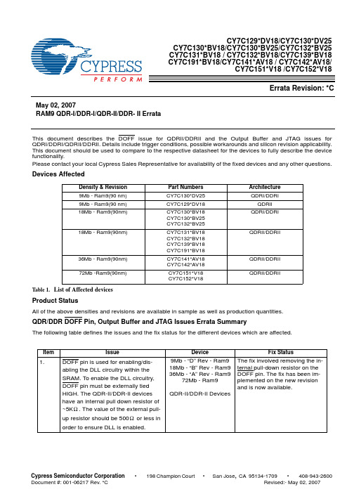
Errata Revision: *CMay 02, 2007RAM9 QDR-I/DDR-I/QDR-II/DDR- II ErrataCY7C129*DV18/CY7C130*DV25CY7C130*BV18/CY7C130*BV25/CY7C132*BV25CY7C131*BV18 / CY7C132*BV18/CY7C139*BV18CY7C191*BV18/CY7C141*AV18 / CY7C142*AV18/CY7C151*V18 /CY7C152*V18This document describes the DOFF issue for QDRII/DDRII and the Output Buffer and JTAG issues for QDRI/DDRI/QDRII/DDRII. Details include trigger conditions, possible workarounds and silicon revision applicability.This document should be used to compare to the respective datasheet for the devices to fully describe the device functionality.Please contact your local Cypress Sales Representative for availability of the fixed devices and any other questions.Devices AffectedTable 1. List of Affected devicesProduct StatusAll of the above densities and revisions are available in sample as well as production quantities.QDR/DDR DOFF Pin, Output Buffer and JTAG Issues Errata SummaryThe following table defines the issues and the fix status for the different devices which are affected.Density & Revision Part Numbers Architecture 9Mb - Ram9(90 nm)CY7C130*DV25QDRI/DDRI 9Mb - Ram9(90 nm)CY7C129*DV18QDRII 18Mb - Ram9(90nm)CY7C130*BV18CY7C130*BV25CY7C132*BV25QDRI/DDRI18Mb - Ram9(90nm)CY7C131*BV18CY7C132*BV18CY7C139*BV18CY7C191*BV18QDRII/DDRII36Mb - Ram9(90nm)CY7C141*AV18CY7C142*AV18QDRII/DDRII 72Mb -Ram9(90nm)CY7C151*V18CY7C152*V18QDRII/DDRIIItemIssueDeviceFix Status1.DOFF pin is used for enabling/dis-abling the DLL circuitry within the SRAM. To enable the DLL circuitry, DOFF pin must be externally tied HIGH. The QDR-II/DDR-II devices have an internal pull down resistor of ~5K . The value of the external pull-up resistor should be 500 or less in order to ensure DLL is enabled.9Mb - “D” Rev - Ram918Mb - “B” Rev - Ram936Mb - “A” Rev - Ram972Mb - Ram9QDR-II/DDR-II DevicesThe fix involved removing the in-ternal pull-down resistor on the DOFF pin. The fix has been im-plemented on the new revision and is now available.ΩΩTable 2.Issue Definition and fix status for different devices1. DOFF Pin Issue•ISSUE DEFINITIONThis issue involves the DLL not turning ON properly if a large resistor is used (eg:-10K ) as an external pullup resistor to enable the DLL. If a 10K or higher pullup resistor is used externally, the voltage on DOFF is not high enough to enable the DLL.•PARAMETERS AFFECTEDThe functionality of the device will be affected because of the DLL is not turning ON properly. When the DLL is enabled, all AC and DC parameters on the datasheet are met. •TRIGGER CONDITION(S)Having a 10K or higher external pullup resistor for disabling the DOFF pin.•SCOPE OF IMPACTThis issue will alter the normal functionality of the QDRII/DDRII devices when the DLL is disabled.•EXPLANATION OF ISSUEFigure 1 shows the DOFF pin circuit with an internal 5K internal resistor. The fix planned is to disable the internal 5K leaker.•WORKAROUND2.O/P Buffer enters a locked up unde-fined state after controls or clocks are left floating. No proper read/write access can be done on the device until a dummy read is performed.9Mb - “D” Rev - Ram918Mb - “B” Rev - Ram936Mb - “A” Rev - Ram972Mb - Ram9QDR-I/DDR-I/QDR-II/DDR-II Devices The fix has been implemented onthe new revision and is now avail-able.3.The EXTEST function in the JTAG test fails when input K clock is floating in the JTAG mode.9Mb - “D” Rev - Ram918Mb - “B” Rev - Ram936Mb - “A” Rev - Ram972Mb - Ram9QDR-I/DDR-I/QDR-II/DDR-II DevicesThe fix involved bypassing the ZQ circuitry in JTAG mode. This was done by overriding the ZQ circuit-ry by the JTAG signal. The fix has been implemented on the new re-vision and is now available.Figure 1.DOFF pin with the 5K internal resistorItemIssueDeviceFix StatusΩΩΩΩΩΩThe workaround is to have a low value of external pullup resistor for the DOFF pin (recommended value is <500). When DOFF pins from multiple QDR devices are connected through the same pull-up resistors on the board, it is recommended that this DOFF pin be directly connected to Vdd due to the lower effective resistance since the "leakers" are in parallel.Figure 2 shows the proposed workaround and the fix planned.•FIXSTATUSFix involved removing the internal pull-down resistor on the DOFF pin. The fix has been implemented on the new revision and is now available. The new revision is an increment of the existing revision. The following table lists the devices affected, current revision and the new revision after the fix.Table 3.List of Affected Devices and the new revison2.Output Buffer IssueFigure 2.Proposed workaround with the 500 external pullupCurrent Revision New Revision after the FixCY7C129*DV18CY7C129*EV18CY7C131*BV18CY7C131*CV18CY7C132*BV18CY7C132*CV18CY7C139*BV18CY7C139*CV18CY7C191*BV18CY7C191*CV18CY7C141*AV18CY7C141*BV18CY7C142*AV18CY7C142*BV18CY7C151*V18CY7C151*AV18CY7C152*V18CY7C152*AV18ΩΩ•ISSUE DEFINITIONThis issue involves the output buffer entering an unidentified state when the input signals (only Control signals or Clocks) are floating during reset or initialization of the memory controller after power up. •PARAMETERS AFFECTEDNo timing parameters are affected. The device may drive the outputs even though the read operation is not enabled. A dummy read is performed to clear this condition.•TRIGGER CONDITION(S)Input signals(namely RPS# for QDR-I/QDRII , WE# and LD# for DDR-I/DDRII) or Clocks (K/K# and/or C/C#) are floating during reset or initialization of the memory controller after power up.•SCOPE OF IMPACTThis issue will jeopardize any number of writes or reads which take place after the controls or clock are left floating. This can occur anywhere in the SRAM access ( all the way from power up of the memory device to transitions taking place for read/write accesses to the memory device) if the above trigger conditions are met.•EXPLANATION OF ISSUEFigure 3 shows the output register Reset circuit with an SR Latch circled. This latch has two inputs with one of them coming from some logic affected by the clock and RPS#(QDR) or WE# and LD#(DDR).The issue happens when clocks are glitching/toggling with controls floating. This will cause the SR latch to be taken into an unidentified state. The SR Latch will need to be reset by a dummy read operation if this happens. Array•WORKAROUNDThis is viable only if the customer has the trigger conditions met during reset or initialization of the memory controller after power up. In order for the workaround to perform properly, Cypress recommends the insertion of a minimum of 16 “dummy” READ operations to every SRAM device on the board prior to writing any meaningful data into the SRAM. After this one “dummy” READ operation, the device will perform properly.“Dummy” READ is defined as a read operation to the device that is not meant to retrieve required data. The “dummy” READ can be to any address location in the SRAM. Refer to Figure 4 for the dummy read implemen-tation.In systems where multiple SRAMs with multiple RPS# lines are used, a dummy read operation will have to be performed on every SRAM on the board. Below is an example sequence of events that can be performed before valid access can be performed on the SRAM.1) Initialize the Memory Controller2) Assert RPS# Low for each of the memory devicesNote:For all devices with x9 bus configuration, the following sequence needs to be performed:1) For the 72M / 36M / 18M x9 devices drive address pin A2 / A10 / A3 low respectively and perform dummyread.2) For the 72M / 36M / 18M x9 devices drive address pin A2 / A10 / A3 high respectively and perform dummyread.If the customer has the trigger conditions met during normal access to the memory then there is no workaround at this point.•FIX STATUSThe fix has been implemented on the new revision and is now available. The new revision is an increment of the existing revision. Please refer to Table 4 for the list of devices affected, current revision and the new revision after the fix.3. JTAG Mode Issue•ISSUE DEFINITIONIf the input clock (K Clock) is left floating when the device is in JTAG mode, spurious high frequency noise on this input can be interpreted by the device as valid clocks. This could cause the impedance matching circuitry (ZQ) on the QDR/DDR devices to periodically load itself with incorrect values. These incorrect values in the ZQ register could force the outputs into a High-Impedance state. The ZQ circuitry requires at least 1000 valid K clock cycles to drive the outputs from high impedance to low impedance levels.•PARAMETERS AFFECTEDThis issue only affects the EXTEST command when the device is in the JTAG mode. The normal functionality of the device will not be affected.•TRIGGER CONDITION(S)EXTEST command executed immediately after power-up without providing any K clock cycles.•SCOPE OF IMPACTThis issue only impacts the EXTEST command when device is tested in the JTAG mode. Normal functionality of the device is not affected. •EXPLANATION OF ISSUEImpedance matching circuitry (ZQ) is present on the QDR/DDR devices to set the desired impedance on the outputs. This ZQ circuitry is updated every 1000 clock cycles of K clock to ensure that the impedance of the O/P is set to valid state. However, when the device is operated in the JTAG mode immediately after power-up, high frequency noise on the input K clock can be treated by the ZQ circuitry as valid clocks thereby setting the outputs in to a high-impedance mode. If a minimum of 1000 valid K clocks are applied before performing the JTAG test, this should clear the ZQ circuitry and ensure that the outputs are driven to valid impedance levels.•WORKAROUNDElimination of the issue: After power-up, before any valid operations are performed on the device, insert a minimum of 1000 valid clocks on K input.•FIX STATUSThe fix involved bypassing the ZQ circuitry in JTAG mode. This was done by overriding the ZQ circuitry by the JTAG signal. The fix has been implemented on the new revision and is now available. The new revision is an increment of the existing revision. Please refer to Table 4 for the list of devices affected, current revision and the new revision after the fix..Table 4.List of Affected devices and the new revisionCurrent Revision New Revision after the FixCY7C129*DV18CY7C129*EV18CY7C130*DV25CY7C130*EV25CY7C130*BV18CY7C130*CV18CY7C130*BV25CY7C130*CV25CY7C132*BV25CY7C132*CV25CY7C131*BV18CY7C131*CV18CY7C132*BV18CY7C132*CV18CY7C139*BV18CY7C139*CV18CY7C191*BV18CY7C191*CV18CY7C141*AV18CY7C141*BV18CY7C142*AV18CY7C142*BV18CY7C151*V18CY7C151*AV18CY7C152*V18CY7C152*AV18ReferencesAll 90nm QDRI/DDRI/QDRII/DDRII datasheets:-Table 5.List of Datasheet spec# for the Affected devicesSpec#Part#DensityArchitecture38-05628CY7C1304DV259-MBIT QDR(TM) SRAM 4-WORD BURST 38-05632CY7C1308DV259-MBIT DDR-I SRAM 4-WORD BURST 001-00350CY7C1292DV18/1294DV189-MBIT QDR- II(TM) SRAM 2-WORD BURST 38-05621CY7C1316BV18/1916BV18/1318BV18/1320BV1818-MBIT DDR-II SRAM 2-WORD BURST 38-05622CY7C1317BV18/1917BV18/1319BV18/1321BV1818-MBIT DDR-II SRAM 4-WORD BURST 38-05623CY7C1392BV18/1393BV18/1394BV1818-MBIT DDR-II SIO SRAM 2-WORD BURST 38-05631CY7C1323BV2518-MBIT DDR-I SRAM 4-WORD BURST 38-05630CY7C1305BV25/1307BV2518-MBIT QDR(TM) SRAM 4-WORD BURST 38-05627CY7C1303BV25/1306BV2518-MBIT QDR(TM) SRAM 2-WORD BURST 38-05629CY7C1305BV18/1307BV1818-MBIT QDR(TM) SRAM 4-WORD BURST 38-05626CY7C1303BV18/1306BV1818-MBIT QDR(TM) SRAM 2-WORD BURST 38-05619CY7C1310BV18/1910BV18/1312BV18/1314BV1818-MBIT QDR - II (TM) SRAM 2-WORD BURST 38-05620CY7C1311BV18/1911BV18/1313BV18/1315BV1818-MBIT QDR - II SRAM 4-WORD BURST 38-05615CY7C1410AV18/1425AV18/1412AV18/1414AV1836-MBIT QDR-II(TM) SRAM 2-WORD BURST 38-05614CY7C1411AV18/1426AV18/1413AV18/1415AV1836-MBIT QDR(TM)-II SRAM 4-WORD BURST 38-05616CY7C1416AV18/1427AV18/1418AV18/1420AV1836-MBIT DDR-II SRAM 2-WORD BURST 38-05618CY7C1417AV18/1428AV18/1419AV18/1421AV1836-MBIT DDR-II SRAM 4-WORD BURST 38-05617CY7C1422AV18/1429AV18/1423AV18/1424AV1836-MBIT DDR-II SIO SRAM 2-WORD BURST 38-05489CY7C1510V18/1525V18/1512V18/1514V1872-MBIT QDR-II SRAM 2-WORD BURST 38-05363CY7C1511V18/1526V18/1513V18/1515V1872-MBIT QDR(TM)-II SRAM 4-WORD BURST 38-05563CY7C1516V18/1527V18/1518V18/1520V1872-MBIT DDR-II SRAM 2-WORD BURST 38-05565CY7C1517V18/1528V18/1519V18/1521V1872-MBIT DDR-II SRAM 4-WORD BURST 38-05564CY7C1522V18/1529V18/1523V18/1524V1872-MBITDDR-II SIO SRAM 2-WORD BURSTDocument History PageDocument Title: RAM9 QDR-I/DDR-I/QDR-II/DDR- II Errata Document #: 001-06217 Rev. *CREV.ECN NO.IssueDateOrig. ofChange Description of Change**419849See ECN REF New errata for Ram9 QDR2/DDR2 SRAMs.*A493936See ECN QKS Added Output buffer and JTAG mode issues, Item#2 and #3Added 9Mb QDR-II Burst of 2 and QDR-1/DDR-I part numbers.*B733176See ECN NJY Added missing part numbers in the title for Spec#’s 38-05615,38-05614,38-05363,38-05563 on Table 5 on page 7.*C1030020 See ECN TBE Updated the fix status of the three issues, and modified the description forthe Output Buffer workaround for x9 devices on page 5.。
常用手机名词解释 通信技术参数全方位解析教材

常用手机名词解释通信技术参数全方位解析来源:段永超的日志WCDMA网络WCDMA是一种由3GPP具体制定的,基于GSM MAP核心网,UTRAN(UMTS陆地无线接入网)为无线接口的第三代移动通信系统。
目前WCDMA有Release 99、Release 4、Release 5、Release 6等版本。
WCDMA (宽带码分多址)是一个ITU(国际电信联盟)标准,它是从码分多址(CDMA)演变来的,在官方上被认为是IMT-2000的直接扩展,与现在市场上通常提供的技术相比,它能够为移动和手提无线设备提供更高的数据速率。
WCDMA采用直接序列扩频码分多址(DS-CDMA)、频分双工(FDD)方式,码片速率为3.84Mcps,载波带宽为5MHz.基于Release 99/ Release 4版本,可在5MHz的带宽内,提供最高384kbps的用户数据传输速率。
WCDMA能够支持移动/手提设备之间的语音、图象、数据以及视频通信,速率可达2Mb/s(对于局域网而言)或者384Kb/s(对于宽带网而言)。
输入信号先被数字化,然后在一个较宽的频谱范围内以编码的扩频模式进行传输。
窄带CDMA使用的是200KHz宽度的载频,而WCDMA使用的则是一个5MHz 宽度的载频。
WCDMA全名是Wideband CDMA(宽带分码多工存取),是具备代表性的3G移动通信技术,WCDMA可支持384Kbps~2Mbps的数据传输速率。
主导运营商:中国联通(新联通,成立于2008年10月15日,由中国联通、中国网通合并而成。
)是国内WCDMA的主导运营商。
WCDMA终端在国内市场上已很常见。
全球WCDMA用户累计已达3亿户,日韩、欧洲都有一些WCDMA运营商,如日本电信、澳大利亚Telstra、爱尔兰O2、葡萄牙Vodafone等,预计在今年全球将再部署约50个WCDMA商用网络、50个HSDPA商用网络和120个HSUPA商用网络。
莫悟 UC-8200 系列双核麒麟A7 1GHz IIoT 网关说明书

UC-8200SeriesArm Cortex-A7dual-core1GHz IIoT gateways with built-in LTE Cat.4,1mini PCIe expansion slot for a Wi-Fi module,1CAN port,4DIs,4DOsFeatures and Benefits•Armv7Cortex-A7dual-core1GHz•Moxa Industrial Linux with10-year superior long-term support•LTE-ready computer with Verizon/AT&T certification and industrial-grade CE/FCC/UL certifications•Dual-SIM slots•2auto-sensing10/100/1000Mbps Ethernet ports•Integrated LTE Cat.4module with US/EU/APAC band support•1CAN port supports CAN2.0A/B•microSD socket for storage expansion•Programmable LEDs and a programmable button for easy installation andmaintenance•-40to85°C wide temperature range and-40to70°C with LTE enabledCertificationsIntroductionThe UC-8200computing platform is designed for embedded data acquisition applications.The computer comes with dual RS-232/422/485serial ports,dual10/100/1000Mbps Ethernet ports,and one CAN port as well as dual Mini PCIe socket to support Wi-Fi/cellular modules.These versatile capabilities let users efficiently adapt the UC-8200to a variety of complex communications solutions.The UC-8200is built around a Cortex-A7dual core processor that has been optimized for use in energy monitoring systems,but is widely applicable to a variety of industrial solutions.With flexible interfacing options,this tiny embedded computer is a reliable and secure gateway for data acquisition and processing at field sites as well as a useful communications platform for many other large-scale deployments.Wide temperature LTE-enabled models are available for extended temperature applications.All units are thoroughly tested in a testing chamber, guaranteeing that the LTE-enabled computing platforms are suitable for wide-temperature applications.AppearanceUC-8210UC-8220SpecificationsComputerCPU Armv7Cortex-A7dual-core1GHzDRAM2GB DDR3LStorage Pre-installed8GB eMMCPre-installed OS Moxa Industrial Linux(Debian9,Kernel4.4)See /MILExpansion Slots MicroSD(SD3.0)socket x1Computer InterfaceTPM UC-8210-T-LX-S:TPM v2.0UC-8220-T-LX-AP-S:TPM v2.0UC-8220-T-LX-EU-S:TPM v2.0UC-8220-T-LX-US-S:TPM v2.0Ethernet Ports Auto-sensing10/100/1000Mbps ports(RJ45connector)x2 Serial Ports RS-232/422/485ports x2,software selectable(DB9male) CAN Ports CAN2.0A/B x1(DB9male)Digital Input DIs x4Digital Output DOs x4USB2.0USB2.0hosts x1,type-A connectorsWi-Fi Antenna Connector RP-SMA x2(UC-8220only)Cellular Antenna Connector SMA x2(UC-8220only)GPS Antenna Connector SMA x1(UC-8220only)Expansion Slots mPCIe slot x2(UC-8220-T-LX)mPCIe slot x1(UC-8220-T-LX US/EU/AP models)SIM Format Nano(UC-8220only)Number of SIMs2(UC-8220only)Buttons Programmable buttonEthernet InterfaceMagnetic Isolation Protection 1.5kV(built-in)Serial InterfaceConsole Port1x4-pin header to DB9console portData Bits5,6,7,8Parity None,Even,Odd,Space,MarkStop Bits1,1.5,2Serial SignalsRS-232TxD,RxD,RTS,CTS,DTR,DSR,DCD,GNDRS-422Tx+,Tx-,Rx+,Rx-,GNDRS-485-2w Data+,Data-,GNDRS-485-4w Tx+,Tx-,Rx+,Rx-,GNDCAN InterfaceNo.of Ports1Connector DB9maleBaudrate10to1000kbpsIndustrial Protocols CAN2.0A,CAN2.0BIsolation2kV(built-in)Signals CAN_H,CAN_L,CAN_GND,CAN_SHLD,CAN_V+,GNDDigital InputsConnector Screw-fastened Euroblock terminalDry Contact Off:openOn:short to GNDIsolation3K VDCSensor Type Wet contact(NPN)Dry contactWet Contact(DI to COM)On:10to30VDCOff:0to3VDCDigital OutputsConnector Screw-fastened Euroblock terminalCurrent Rating200mA per channelI/O Type SinkVoltage24VDC nominal,open collector to30VDCCellular InterfaceCellular Standards LTE CAT-4Band Options US model:LTE Bands:Band2(1900MHz)/Band4(1700MHz)/Band5(850MHz)/Band13(700MHz)/Band14(700MHz)UMTS Bands:Band2(1900MHz)/Band5(850MHz)Carrier Approval:Verizon,AT&TEU model:LTE Bands:Band1(2100MHz)/Band3(1800MHz)/Band5(850MHz)/Band7(2600MHz)/Band8(900MHz)/LTE Band20(800MHz)UMTS Bands:Band1(2100MHz)/Band2(1900MHz)/Band5(850MHz)/Band8(900MHz)AP model:LTE Bands:Band1(2100MHz)/Band3(1800MHz)/Band5(850MHz)/Band7(2600MHz)/Band8(900MHz)/Band28(700MHz)UMTS Bands:Band1(2100MHz)/Band2(1900MHz)/Band5(850MHz)/Band8(900MHz)GPS InterfaceReceiver Types72-channel u-blox M8engineGPS/GLONASS/GalileoAccuracy Position:2.5m CEPSBAS:2.0m CEPAcquisition Aided starts:3secCold starts:26secSensitivity Cold starts:-148dBmTracking:-164dBmTime Pulse0.25Hz to10MHzLED IndicatorsSystem Power x2Programmable x1SIM card indicator x1Wireless Signal Strength Cellular/Wi-Fi x6Power ParametersNo.of Power Inputs Redundant dual inputsInput Voltage12to48VDCPower Consumption10WInput Current0.8A@12VDCReliabilityAlert Tools External RTC(real-time clock)Automatic Reboot Trigger External WDT(watchdog timer)Physical CharacteristicsDimensions141.5x120x39mm(5.7x4.72x1.54in)for UC-8220141.5x120x27mm(5.7x4.72x1.06in)for UC-8210Housing SECCMetalInstallation DIN-rail mounting,Wall mounting(with optional kit)IP Rating IP30Weight UC-8210:560g(1.23lb)UC-8220:750g(1.65lb)Environmental LimitsAmbient Relative Humidity5to95%(non-condensing)Operating Temperature UC-8210-T-LX:-40to85°C(-40to185°F)UC-8210-T-LX-S:-40to85°C(-40to185°F)UC-8220-T-LX:-40to70°C(-40to158°F)UC-8220-T-LX-US-S:-40to70°C(-40to158°F)UC-8220-T-LX-EU-S:-40to70°C(-40to158°F)UC-8220-T-LX-AP-S:-40to70°C(-40to158°F)Storage Temperature(package included)-40to85°C(-40to185°F)Shock IEC60068-2-27Vibration2Grms@IEC60068-2-64,random wave,5-500Hz,1hr per axis(without USB devicesattached)Standards and CertificationsSafety UL62368-1,EN62368-1EMC EN55032/35,EN61000-6-2/-6-4EMI CISPR32,FCC Part15B Class AEMS IEC61000-4-2ESD:Contact:4kV;Air:8kVIEC61000-4-3RS:80MHz to1GHz:10V/mIEC61000-4-4EFT:Power:2kV;Signal:1kVIEC61000-4-6CS:10VIEC61000-4-8PFMFIEC61000-4-5Surge:Power:0.5kV;Signal:1kVHazardous Locations Class I Division2,ATEXCarrier Approvals VerizonAT&TGreen Product RoHS,CRoHS,WEEEMTBFTime UC-8210-T-LX:716,739hrsUC-8210-T-LX-S:708,581hrsUC-8220-T-LX:650,836hrsUC-8220-T-LX-US-S:528,574hrsUC-8220-T-LX-EU-S:528,574hrsUC-8220-T-LX-AP-S:528,574hrsStandards Telcordia(Bellcore)Standard TR/SRWarrantyWarranty Period5yearsDetails See /warrantyPackage ContentsDevice1x UC-8200Series computerDocumentation1x quick installation guide1x warranty cardInstallation Kit1x DIN-rail kit(preinstalled)1x power jack6x M2.5mounting screws for the cellular module Cable1x console cableDimensionsUC-8210UC-8220Ordering InformationModel Name CPU RAM Storage TPM mPCIe Slot1forLTE ModulemPCIe Slot2forWi-Fi ModuleOperatingTemperatureUC-8210-T-LX1GHz Dual Core2GB8GB–––-40to85°C UC-8210-T-LX-S1GHz Dual Core2GB8GB Built-in––-40to85°C UC-8220-T-LX1GHz Dual Core2GB8GB–Reserved Reserved-40to70°CUC-8220-T-LX-US-S 1GHz Dual Core2GB8GB Built-inUS region LTEmodulepreinstalledReserved-40to70°CUC-8220-T-LX-EU-S 1GHz Dual Core2GB8GB Built-inEurope regionLTE modulepreinstalledReserved-40to70°CUC-8220-T-LX-AP-S 1GHz Dual Core2GB8GB Built-inAPAC region LTEmodulepreinstalledReserved-40to70°CAccessories(sold separately)Power AdaptersPWR-12150-EU-SA-T Locking barrel plug,12VDC,1.5A,100to240VAC,Continental Europe(EU)plug,-40to75°Coperating temperaturePWR-12150-UK-SA-T Locking barrel plug,12VDC,1.5A,100to240VAC,United Kingdom(UK)plug,-40to75°C operatingtemperaturePWR-12150-USJP-SA-T Locking barrel plug,12VDC1.5A,100to240VAC,United States/Japan(US/JP)plug,-40to75°Coperating temperaturePWR-12150-AU-SA-T Locking barrel plug,12VDC,1.5A,100to240VAC,Australia(AU)plug,-40to75°C operatingtemperaturePWR-12150-CN-SA-T Locking barrel plug,12VDC,1.5A,100to240VAC,China(CN)plug,-40to75°C operatingtemperaturePower WiringCBL-PJTB-10Non-locking barrel plug to bare-wire cableCablesCBL-F9DPF1x4-BK-100Console cable with4-pin connector,1mWi-Fi Wireless ModulesUC-8200WiFi-AC Wi-Fi package for UC-8200,includes Wi-Fi module,6screws,1heat sink,1padAntennasANT-LTEUS-ASM-01GSM/GPRS/EDGE/UMTS/HSPA/LTE,omni-directional rubber duck antenna,1dBiANT-LTE-ASM-04BK704-960/1710-2620MHz,LTE omni-directional stick antenna,4.5dBiANT-LTE-OSM-03-3m BK700-2700MHz,multi-band antenna,specifically designed for2G,3G,and4G applications,3m cable ANT-LTE-ASM-05BK704-960/1710-2620MHz,LTE stick antenna,5dBiANT-LTE-OSM-06-3m BK MIMO Multiband antenna with screw-fastened mounting option for700-2700/2400-2500/5150-5850MHzfrequenciesANT-WDB-ARM-0202 2.4/5GHz,panel antenna,2/2dBi,RP-SMA(male)DIN-Rail Mounting KitsUC-8220DIN-rail Mounting Kit DIN-rail mounting kit for UC-8220with4M3screwsWall-Mounting KitsUC-8200Wall-mounting Kit Wall-mounting kit for UC-8200with4M3screws©Moxa Inc.All rights reserved.Updated Jun29,2021.This document and any portion thereof may not be reproduced or used in any manner whatsoever without the express written permission of Moxa Inc.Product specifications subject to change without notice.Visit our website for the most up-to-date product information.。
CY7C1515AV18资料

Page 2 of 31 [+] Feedback
元器件交易网
Logic Block Diagram (CY7C1513AV18)
CY7C1511AV18, CY7C1526AV18 CY7C1513AV18, CY7C1515AV18
18 D[17:0]
A(19:0) 20
■ Variable drive HSTL output buffers
■ JTAG 1149.1 compatible test access port
■ Delay Lock Loop (DLL) for accurate data placement
Configurations
CY7C1511AV18 – 8M x 8 CY7C1526AV18 – 8M x 9 CY7C1513AV18 – 4M x 18 CY7C1515AV18 – 2M x 36
Address Register
21
A(20:0)
2M x 8 Array 2M x 8 Array 2M x 8 Array 2M x 8 Array
Read Data Reg. 32 16
16
Control Logic
RPS
C C
Reg.
Reg. 8 8
Reg.
8
8
8
CQ CQ Q[7:0]
Logic Block Diagram (CY7C1526AV18)
Address Register
21
A(20:0)
2M x 9 Array 2M x 9 Array 2M x 9 Array 2M x 9 Array
Read Data Reg. 36 18
4G TD

4G TD-LTE将风卷中国无线宽带市场正当长期演进技术Long-Term Evolution (LTE)和WiMax在全球电信业大力推进时,前者(LTE)也是最强大的4G 移动通讯主导技术,正异军突起,迅速占领中国市场。
虽然Qualcomm 和Yota两家公司的TD-LTE尚未成熟,但很多国内外的无线运营公司都相继转向TD-LTE。
IBM数据显示,67%运营商正考虑使用LTE,因为这是他们未来市场的主要来源。
上述消息也证实了IBM的这一说法。
而只有8%的运营商考虑使用WiMAX。
尽管WiMax 可以给其客户提供市场上传输速度最快的网络,但仍然不是LTE技术的竞争对手。
TD-LTE是第一个4G无线移动宽带网络数据标准,由中国最大的电信运营商--中国移动修订与发布。
在进行一系列的现场试验后,预计在未来2年内步入商用期。
爱立信副总裁Ulf Ewaldsson说:“中国工信部和中国移动将在今年第四季度进行大规模现场试验,届时,爱立信将助之一臂之力。
”编辑本段4G的概念介绍就在3G通信技术正处于酝酿之中时,更高的技术应用已经在实验室进行研发。
因此在人们期待第三代移动通信系统所带来的优质服务的同时,第四代移动通信系统的最新技术也在实验室悄然进行当中。
那么到底什么是4G通信呢?到2009年为止人们还无法对4G通信进行精确地定义,有人说4G通信的概念来自其他无线服务的技术,从无线应用协定、全球袖珍型无线服务到3G;有人说4G通信是一个超越2010年以外的研究主题,4G通信是系统中的系统,可利用各种不同的无线技术;但不管人们对4G通信怎样进行定义,有一点人们能够肯定的是4G通信可能是一个比3G通信更完美的新无线世界,它可创造出许多消费者难以想象的应用。
4G最大的数据传输速率超过100Mbit/s,这个速率是移动电话数据传输速率的1万倍,也是3G移动电话速率的50倍。
4G手机可以提供高性能的汇流媒体内容,并通过ID应用程序成为个人身份鉴定设备。
国内外压敏电阻型号及参数

国内外压敏电阻型号及参数压敏电阻220V电压的电路国内型号:MYG14K471(对应的国外型号:US 470NR-14D)MYG05K471(对应的国外型号:US 470NR-5D)22V左右的电路国内型号:MYG14K470(对应的国外型号:US 470NR-14D)MYG05K470(对应的国外型号:US 470NR-5D)。
压敏电阻型号及参数压敏电阻压敏电阻“压敏电阻"是中国大陆的名词,意思是在一定电流电压范围内电阻值随电压而变,或者是说"电阻值对电压敏感"的阻器。
英文名称叫“Voltage Dependent Resistor”简写为“VDR”, 或者叫做“Varistor"。
压敏电阻器的电阻体材料是半导体,所以它是半导体电阻器的一个品种。
现在大量使用的"氧化锌"(ZnO)压敏电阻器,它的主体材料有二价元素(Zn)和六价元素氧(O)所构成。
所以从材料的角度来看,氧化锌压敏电阻器是一种“Ⅱ-Ⅵ族氧化物半导体”。
在中国台湾,压敏电阻器称为"突波吸收器",有时也称为“电冲击(浪涌)抑制器(吸收器)”。
目录[]1、压敏电阻电路的“安全阀”作用2、压敏电阻的应用类型3、保护用压敏电阻的基本性能4. 压敏电阻的基本参数1、压敏电阻电路的“安全阀”作用2、压敏电阻的应用类型3、保护用压敏电阻的基本性能4. 压敏电阻的基本参数1、压敏电阻电路的“安全阀”作用压敏电阻有什么用?压敏电阻的最大特点是当加在它上面的电压低于它的阀值" UN"时,流过它的电流极小,相当于一只关死的阀门,当电压超过UN时,流过它的电流激增,相当于阀门打开。
利用这一功能,可以抑制电路中经常出现的异常过电压,保护电路免受过电压的损害。
2、压敏电阻的应用类型不同的使用场合,应用压敏电阻的目的,作用在压敏电阻上的电压/电流应力并不相同,因而对压敏电阻的要求也不相同,注意区分这种差异,对于正确使用是十分重要的。
M-SYSTEM CO LTD 远程I O R7 系列 R7C规格书
◆适用标准 不写入: 符合CE /UL: 符合UL、CE
主要的功能与特长
CC-Link少点数输入输出模块R7C是用PLC和CC-Link连接模拟 量输入输出和接点输入输出的模块。 通过连接基本模块和增设模块,可作为模拟量输入输出和接 点输入输出混合共存的模块使用。也可作为接点32点输入模 块、接点32点输出模块、接点输入与输出各16点的模块使 用。要注意的是接点输出模块R7C-DC16A、DC16B、DC8 E只能连接增设接点输入模块R7C-EC8A、EC16A、EC8B、 EC16B、EC8C。接点继电器8点输出模块R7C-DC8C、遥控 继电器控制用4点输出模块R7C-RR4不能连接增设模块。 输入输出范围、输入传感器(热电偶和热电阻)的设定可通 过前端面板的DIP开关统一设定。也可通过组态软件(机型: R7CON)分别设定每一点的输入与输出。通过组态软件还可 进行零点及量程的调整、标定的设定、温度单位的变更等。
◎
●
—
●
○
接收的数据为CRC错误,无法应答
●
●
-
◎
○
通讯正常
◎
●
-
●
○
不接收发送至本站的数据
●
●
-
◎
○
按时间序列响应,但是更新数据为CRC错误
◎
●
-
●
○
本站的数据为CRC错误
●
●
-
◎
○
链接没有起动
◎
●
-
无发送至本站的数据或由于干扰而无法接收发送至本站的数据
●
○
(从主站发送过来的数据量不足)
●
●
因为断线等原因无法接收数据
附带品
CD4017BD中文资料

Data sheet acquired from Harris Semiconductor SCHS027C − Revised February 2004The CD4017B and CD4022B types are supplied in 16-lead hermetic dual-in-line ceramic packages (F3A suffix), 16-lead dual-in-line plastic package (E suffix), 16-lead small-outline packages (NSR suffix),and 16-lead thin shrink small-outline packages (PW and PWR suffixes). The CD4017B types also are supplied in 16-lead small-outline packages (M and M96 suffixes).ripple-clock the succeeding device in a multi-device counting chain.PACKAGING INFORMATIONOrderable Device Status(1)PackageType PackageDrawingPins PackageQtyEco Plan(2)Lead/Ball Finish MSL Peak Temp(3)89270AKB3T OBSOLETE0TBD Call TI Call TICD4017BE ACTIVE PDIP N1625Pb-Free(RoHS)CU NIPDAU N/A for Pkg TypeCD4017BEE4ACTIVE PDIP N1625Pb-Free(RoHS)CU NIPDAU N/A for Pkg Type CD4017BF ACTIVE CDIP J161TBD A42SNPB N/A for Pkg Type CD4017BF3A ACTIVE CDIP J161TBD A42SNPB N/A for Pkg Type CD4017BF3AS2534OBSOLETE CDIP J16TBD Call TI Call TI CD4017BM ACTIVE SOIC D1640Green(RoHS&no Sb/Br)CU NIPDAU Level-1-260C-UNLIMCD4017BM96ACTIVE SOIC D162500Green(RoHS&no Sb/Br)CU NIPDAU Level-1-260C-UNLIMCD4017BM96E4ACTIVE SOIC D162500Green(RoHS&no Sb/Br)CU NIPDAU Level-1-260C-UNLIMCD4017BM96G4ACTIVE SOIC D162500Green(RoHS&no Sb/Br)CU NIPDAU Level-1-260C-UNLIMCD4017BME4ACTIVE SOIC D1640Green(RoHS&no Sb/Br)CU NIPDAU Level-1-260C-UNLIMCD4017BMG4ACTIVE SOIC D1640Green(RoHS&no Sb/Br)CU NIPDAU Level-1-260C-UNLIMCD4017BNSR ACTIVE SO NS162000Green(RoHS&no Sb/Br)CU NIPDAU Level-1-260C-UNLIMCD4017BNSRE4ACTIVE SO NS162000Green(RoHS&no Sb/Br)CU NIPDAU Level-1-260C-UNLIMCD4017BNSRG4ACTIVE SO NS162000Green(RoHS&no Sb/Br)CU NIPDAU Level-1-260C-UNLIMCD4017BPW ACTIVE TSSOP PW1690Green(RoHS&no Sb/Br)CU NIPDAU Level-1-260C-UNLIMCD4017BPWE4ACTIVE TSSOP PW1690Green(RoHS&no Sb/Br)CU NIPDAU Level-1-260C-UNLIMCD4017BPWG4ACTIVE TSSOP PW1690Green(RoHS&no Sb/Br)CU NIPDAU Level-1-260C-UNLIMCD4017BPWR ACTIVE TSSOP PW162000Green(RoHS&no Sb/Br)CU NIPDAU Level-1-260C-UNLIMCD4017BPWRE4ACTIVE TSSOP PW162000Green(RoHS&no Sb/Br)CU NIPDAU Level-1-260C-UNLIMCD4017BPWRG4ACTIVE TSSOP PW162000Green(RoHS&no Sb/Br)CU NIPDAU Level-1-260C-UNLIMCD4022BE ACTIVE PDIP N1625Pb-Free(RoHS)CU NIPDAU N/A for Pkg TypeCD4022BEE4ACTIVE PDIP N1625Pb-Free(RoHS)CU NIPDAU N/A for Pkg Type CD4022BF ACTIVE CDIP J161TBD A42SNPB N/A for Pkg Type CD4022BF3A ACTIVE CDIP J161TBD A42SNPB N/A for Pkg Type CD4022BNSR ACTIVE SO NS162000Green(RoHS&no Sb/Br)CU NIPDAU Level-1-260C-UNLIMCD4022BNSRE4ACTIVE SO NS162000Green(RoHS&no Sb/Br)CU NIPDAU Level-1-260C-UNLIMOrderable Device Status(1)PackageType PackageDrawingPins PackageQtyEco Plan(2)Lead/Ball Finish MSL Peak Temp(3)CD4022BNSRG4ACTIVE SO NS162000Green(RoHS&no Sb/Br)CU NIPDAU Level-1-260C-UNLIMCD4022BPW ACTIVE TSSOP PW1690Green(RoHS&no Sb/Br)CU NIPDAU Level-1-260C-UNLIMCD4022BPWE4ACTIVE TSSOP PW1690Green(RoHS&no Sb/Br)CU NIPDAU Level-1-260C-UNLIMCD4022BPWG4ACTIVE TSSOP PW1690Green(RoHS&no Sb/Br)CU NIPDAU Level-1-260C-UNLIMCD4022BPWR ACTIVE TSSOP PW162000Green(RoHS&no Sb/Br)CU NIPDAU Level-1-260C-UNLIMCD4022BPWRE4ACTIVE TSSOP PW162000Green(RoHS&no Sb/Br)CU NIPDAU Level-1-260C-UNLIMCD4022BPWRG4ACTIVE TSSOP PW162000Green(RoHS&no Sb/Br)CU NIPDAU Level-1-260C-UNLIM JM38510/05651BEA ACTIVE CDIP J161TBD A42SNPB N/A for Pkg Type (1)The marketing status values are defined as follows:ACTIVE:Product device recommended for new designs.LIFEBUY:TI has announced that the device will be discontinued,and a lifetime-buy period is in effect.NRND:Not recommended for new designs.Device is in production to support existing customers,but TI does not recommend using this part in a new design.PREVIEW:Device has been announced but is not in production.Samples may or may not be available.OBSOLETE:TI has discontinued the production of the device.(2)Eco Plan-The planned eco-friendly classification:Pb-Free(RoHS),Pb-Free(RoHS Exempt),or Green(RoHS&no Sb/Br)-please check /productcontent for the latest availability information and additional product content details.TBD:The Pb-Free/Green conversion plan has not been defined.Pb-Free(RoHS):TI's terms"Lead-Free"or"Pb-Free"mean semiconductor products that are compatible with the current RoHS requirements for all6substances,including the requirement that lead not exceed0.1%by weight in homogeneous materials.Where designed to be soldered at high temperatures,TI Pb-Free products are suitable for use in specified lead-free processes.Pb-Free(RoHS Exempt):This component has a RoHS exemption for either1)lead-based flip-chip solder bumps used between the die and package,or2)lead-based die adhesive used between the die and leadframe.The component is otherwise considered Pb-Free(RoHS compatible)as defined above.Green(RoHS&no Sb/Br):TI defines"Green"to mean Pb-Free(RoHS compatible),and free of Bromine(Br)and Antimony(Sb)based flame retardants(Br or Sb do not exceed0.1%by weight in homogeneous material)(3)MSL,Peak Temp.--The Moisture Sensitivity Level rating according to the JEDEC industry standard classifications,and peak solder temperature.Important Information and Disclaimer:The information provided on this page represents TI's knowledge and belief as of the date that it is provided.TI bases its knowledge and belief on information provided by third parties,and makes no representation or warranty as to the accuracy of such information.Efforts are underway to better integrate information from third parties.TI has taken and continues to take reasonable steps to provide representative and accurate information but may not have conducted destructive testing or chemical analysis on incoming materials and chemicals.TI and TI suppliers consider certain information to be proprietary,and thus CAS numbers and other limited information may not be available for release.In no event shall TI's liability arising out of such information exceed the total purchase price of the TI part(s)at issue in this document sold by TI to Customer on an annual basis.TAPE AND REEL INFORMATION*All dimensions are nominalDevicePackage Type Package Drawing Pins SPQReel Diameter (mm)Reel Width W1(mm)A0(mm)B0(mm)K0(mm)P1(mm)W (mm)Pin1Quadrant CD4017BM96SOIC D 162500330.016.4 6.510.3 2.18.016.0Q1CD4017BNSR SO NS 162000330.016.48.210.5 2.512.016.0Q1CD4017BPWR TSSOP PW 162000330.012.47.0 5.6 1.68.012.0Q1CD4022BNSR SO NS 162000330.016.48.210.5 2.512.016.0Q1CD4022BPWRTSSOPPW162000330.012.47.05.61.68.012.0Q1*All dimensions are nominalDevice Package Type Package Drawing Pins SPQ Length(mm)Width(mm)Height(mm) CD4017BM96SOIC D162500333.2345.928.6 CD4017BNSR SO NS162000346.0346.033.0 CD4017BPWR TSSOP PW162000346.0346.029.0 CD4022BNSR SO NS162000346.0346.033.0 CD4022BPWR TSSOP PW162000346.0346.029.0IMPORTANT NOTICETexas Instruments Incorporated and its subsidiaries(TI)reserve the right to make corrections,modifications,enhancements,improvements, and other changes to its products and services at any time and to discontinue any product or service without notice.Customers should obtain the latest relevant information before placing orders and should verify that such information is current and complete.All products are sold subject to TI’s terms and conditions of sale supplied at the time of order acknowledgment.TI warrants performance of its hardware products to the specifications applicable at the time of sale in accordance with TI’s standard warranty.Testing and other quality control techniques are used to the extent TI deems necessary to support this warranty.Except where mandated by government requirements,testing of all parameters of each product is not necessarily performed.TI assumes no liability for applications assistance or customer product design.Customers are responsible for their products and applications using TI components.To minimize the risks associated with customer products and applications,customers should provide adequate design and operating safeguards.TI does not warrant or represent that any license,either express or implied,is granted under any TI patent right,copyright,mask work right, or other TI intellectual property right relating to any combination,machine,or process in which TI products or services are rmation published by TI regarding third-party products or services does not constitute a license from TI to use such products or services or a warranty or endorsement e of such information may require a license from a third party under the patents or other intellectual property of the third party,or a license from TI under the patents or other intellectual property of TI.Reproduction of TI information in TI data books or data sheets is permissible only if reproduction is without alteration and is accompanied by all associated warranties,conditions,limitations,and notices.Reproduction of this information with alteration is an unfair and deceptive business practice.TI is not responsible or liable for such altered rmation of third parties may be subject to additional restrictions.Resale of TI products or services with statements different from or beyond the parameters stated by TI for that product or service voids all express and any implied warranties for the associated TI product or service and is an unfair and deceptive business practice.TI is not responsible or liable for any such statements.TI products are not authorized for use in safety-critical applications(such as life support)where a failure of the TI product would reasonably be expected to cause severe personal injury or death,unless officers of the parties have executed an agreement specifically governing such use.Buyers represent that they have all necessary expertise in the safety and regulatory ramifications of their applications,and acknowledge and agree that they are solely responsible for all legal,regulatory and safety-related requirements concerning their products and any use of TI products in such safety-critical applications,notwithstanding any applications-related information or support that may be provided by TI.Further,Buyers must fully indemnify TI and its representatives against any damages arising out of the use of TI products in such safety-critical applications.TI products are neither designed nor intended for use in military/aerospace applications or environments unless the TI products are specifically designated by TI as military-grade or"enhanced plastic."Only products designated by TI as military-grade meet military specifications.Buyers acknowledge and agree that any such use of TI products which TI has not designated as military-grade is solely at the Buyer's risk,and that they are solely responsible for compliance with all legal and regulatory requirements in connection with such use. TI products are neither designed nor intended for use in automotive applications or environments unless the specific TI products are designated by TI as compliant with ISO/TS16949requirements.Buyers acknowledge and agree that,if they use any non-designated products in automotive applications,TI will not be responsible for any failure to meet such requirements.Following are URLs where you can obtain information on other Texas Instruments products and application solutions:Products ApplicationsAmplifiers AudioData Converters AutomotiveDSP BroadbandClocks and Timers Digital ControlInterface MedicalLogic MilitaryPower Mgmt Optical NetworkingMicrocontrollers SecurityRFID TelephonyRF/IF and ZigBee®Solutions Video&ImagingWirelessMailing Address:Texas Instruments,Post Office Box655303,Dallas,Texas75265Copyright©2008,Texas Instruments Incorporated。
灵巧网关硬件配置表
编号:NS005FATA--
产品名称:NetEye 防火墙版本号:3.1
产品型号:SG-1000(灵巧网关-以太网卡/ADSL -具有VPN 功能)
型号集成网卡配置集成显卡配置型号数量品牌容量数量
型号数量
型号
数量
外频型号数量
型号数量
1U 438*290*44nupro775intel 82559celoen 8001DOM200032MB DiskOn Module
1Intel pro100 s
1kingmax 250 md
1150亿阳网
警
SJY22-B PCI 密码卡
1台湾 SS-200U1
1
产品名称:NetEye 防火墙版本号:3.1
产品型号:SG-1000(灵巧网关-以太网卡/ADSL -无VPN 功能)
型号
集成网卡配置集成显卡配置型号
数量
品牌
容量
数量
型号
数量
型号
数量
外频
型号
数量
型号
数量
硬件配置表
机箱规格
型号主板CPU 网卡
内存加密卡
电源
FLASH 卡
硬件配置
硬件配置
机箱规格型号
主板
CPU FLASH 卡
网卡内存加密卡电源
VPN功能)PN功能)。
PIONEER参数之UMTS参数指标
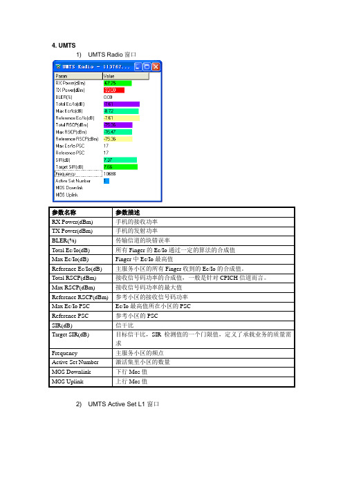
4. UMTS1) UMTS Radio窗口参数名称参数描述RX Power(dBm) 手机的接收功率TX Power(dBm) 手机的发射功率BLER(%) 传输信道的块错误率Total Ec/Io(dB) 所有Finger的Ec/Io通过一定的算法的合成值Max Ec/Io(dB) Finger中Ec/Io最高值Reference Ec/Io(dB) 主服务小区的所有Finger收到的Ec/Io的合成值。
Total RSCP(dBm) 接收信号码功率的合成值,一般是针对CPICH信道而言。
Max RSCP(dBm) 接收信号码功率的最大值Reference RSCP(dBm) 参考小区的接收信号码功率Max Ec/Io PSC Ec/Io最高值所在小区的PSCReference PSC 参考小区的PSCSIR(dB) 信干比Target SIR(dB) 目标信干比,SIR检测值的一个门限值,定义了承载业务的质量需求Frequency 主服务小区的频点Active Set Number 激活集里小区的数量MOS Downlink 下行Mos值MOS Uplink 上行Mos值2) UMTS Active Set L1窗口参数名称参数描述PSC 主扰码Ec/Io(dB) 激活集里小区的Ec/Io值。
RSCP(dBm) 接收到的信号功率强度Locked Num 锁住的Finger个数NodeB 基站名称Distance(m) 基站距离当前测试点的距离3) Throughput窗口参数名称参数描述DL_PHYS_Thr(bps) 下行的物理层吞吐量UL_PHYS_Thr(bps) 上行的物理层吞吐量DL_PDU_Thr(bps) 下行PDU的吞吐量UL_PDU_Thr(bps) 上行PDU的吞吐量DL_SDU_Thr(bps) 下行SDU的吞吐量UL_SDU_Thr(bps) 上行SDU的吞吐量PDU_Err_Rate(%) PDU误包比率PDU_RTX_Rate(%) PDU重传率4) UMTS PRACH窗口参数名称参数描述Max TX Power 手机最大发射功率Signature Mask 符号掩码Sub Cha. Mask 接入网络时使用的信道掩码Spreading Factor 扩频因子Scrambling Code 扰码UL Puncturing 上行编码打孔率Transport Chan. 传输信道的ID号PWR Ramp Step 接入网络时手机发射功率的递增步长Preamble Trans. 允许发送的最大接入试探前缀数5) UMTS RACH窗口参数名称参数描述AICH Status 捕获信道状态Access Slot 接入时隙Last Power Set 最近一次接入网络时的功率设置SFN 系统帧号Preamble Signature 接入信道的接入试探前缀信号AICH Timing 接入网络时所用的时隙数Preambles Txmt 最近一次接入网络时发送的前缀信号数量Message Length 接入脉冲的信息长度参数名称参数描述Reg State 登记状态GMM State GPRS移动管理状态。
- 1、下载文档前请自行甄别文档内容的完整性,平台不提供额外的编辑、内容补充、找答案等附加服务。
- 2、"仅部分预览"的文档,不可在线预览部分如存在完整性等问题,可反馈申请退款(可完整预览的文档不适用该条件!)。
- 3、如文档侵犯您的权益,请联系客服反馈,我们会尽快为您处理(人工客服工作时间:9:00-18:30)。
1 Configuration Pb-free leadwire fD Pb-free PET sleeve 3 CD 4 ~ 6.3 DD
16 1C 25 1E
D Code 3 2 2 Size code 4 ~ 6.3 Ñ Configuration 1 Capacitance tolerance (± 20%) Rated capacitance (10mF) Rated voltage (25V) Series name Type
Shelf Life Marking
After storing the capacitors under no load at 105°C for 1000 hours, and after performing voltage treatment based on JIS C 5101-4 clause 4.1 at 20°C, they will meet the specified value for endurance characteristics listed above.
22 30 36 60
5×5 5×5 6.3 × 5
27 35 46
4×5 5×5 6.3 × 5 6.3 × 5
18 (14) 30 40 50
4×5 5×5 6.3 × 5 6.3 × 5
13 (10) 23 38 48
3 ×5 4 ×5 4 ×5 5×5 6.3 × 5
7.5 11 (9) 15 25 48
– 55 ~ +105°C 4 ~ 50V 0.1 ~ 100µF ± 20% at 120Hz, 20°C After 2 minutes' application of rated voltage, leakage current is not more than 0.01CV or 3 (µA), whichever is greater.
Printed with white color letter on black sleeve.
Radial Lead Type
Type numbering system (Example : 25V 10µF)
fd
Sleeve (P.E.T.)
f D+0.5MAX
UMT 1 E 1 0 0 MDD
(f 3 : P±0.3)
(mm) P ±0.5
1 2 3 4 5 6 7 8 9 10 11 12
L+1MAX
15 MIN
4
f
D 3 4 5 6.3 P 1.0 1.5 2.0 2.5 f d 0.40 0.45 0.45 0.45
• Please refer to page 21 about the end seal configulation.
φ D × L (mm)
Case size
Rated ripple
Size φ3 × 5 is available for capacitors marked " " Figures in ( ) are for φ 3 product.
Rated Ripple (mArms) at 105°C 120Hz
Measurement frequency : 120Hz
Stability at Low Temperature
Rated voltage (V) Z– 25°C / Z+20°C Impedance ratio ZT / Z20 (MAX.) Z– 40°C / Z+20°C After 1000 hours' application of rated voltage at 105°C, capacitors meet the characteristic requirements listed at right.
CAT.8100V
MV
Long life
MT
High Temperature
MA
Specifications
Item Category Temperature Range Voltage Range Rated Capacitance Range Rated Capacitance Tolerance Leakage Current tan δ Performance Characteristics
Frequency coefficient of rated ripple current
Frequency Coefficient 50 Hz 0.70 120 Hz 1.00 300 Hz 1.17 1 kHz 1.36 10 kHz ~ 1.50
Please refer to page 21, 22, 23 about the formed or taped product spec. Please refer to page 3 for the minimum order quantity.
Capacitance change tan δ Leakage current
Endurance
Within ±25% of initial value (φ 3mm unit,and < 16V) = Within ±20% of initial value ( > 25V) =
200% or less of initial specified value Initial specified value or less
Measurement frequency : 120Hz, Temperature : 20°C Rated voltage (V) tan δ ( MAX.)
4 0.37
6.3 0.28 4 6 12
10 0.24 6.3 3 8
16 0.20 10 3 5
25 0.16 16 2 4
35 50 Figures in ( ) are for 0.13 (0.14) 0.12 (0.14) φ 3 product. 25 2 3 35 2 3 50 2 3
4 0G
6.3 0J
10 1A
0.1 0.22 0.33 0.47 1 2.2 3.3 4.7 10 22 33 47 100
0R1 R22 R33 R47 010 2R2 3R3 4R7 100 220 330 470 101
4×5 5×5 5×5 6.3 × 5
22 30 36 60
4×5 5×5 5×5 6.3 × 5
元器件交易网
ALUMINUM ELECTROLYTIC CAPACITORS
MT
5mmL, Wide Temperature Range
series
Wide temperature range of – 55 ~ +105°C, with 5mm height. Adapted to the RoHS directive (2002/95/EC).
f
Dimensions
Cap.(µF) V Code
2 For f 3mm unit, place size code of 2 to 12th digit.
35 1V 50 1H 4×5 1.0 4×5 2.6 4×5 3.2 4×5 3.8 6.2 (5.9) 4×5 11 (9) 4×5 14 4×5 19 5×5 30 6.3 × 5